JP4095731B2 - Semiconductor device manufacturing method and semiconductor device - Google Patents
Semiconductor device manufacturing method and semiconductor device Download PDFInfo
- Publication number
- JP4095731B2 JP4095731B2 JP31723398A JP31723398A JP4095731B2 JP 4095731 B2 JP4095731 B2 JP 4095731B2 JP 31723398 A JP31723398 A JP 31723398A JP 31723398 A JP31723398 A JP 31723398A JP 4095731 B2 JP4095731 B2 JP 4095731B2
- Authority
- JP
- Japan
- Prior art keywords
- polishing
- metal layer
- abrasive
- acid
- conductive film
- Prior art date
- Legal status (The legal status is an assumption and is not a legal conclusion. Google has not performed a legal analysis and makes no representation as to the accuracy of the status listed.)
- Expired - Lifetime
Links
Images


Classifications
-
- H—ELECTRICITY
- H01—ELECTRIC ELEMENTS
- H01L—SEMICONDUCTOR DEVICES NOT COVERED BY CLASS H10
- H01L21/00—Processes or apparatus adapted for the manufacture or treatment of semiconductor or solid state devices or of parts thereof
- H01L21/02—Manufacture or treatment of semiconductor devices or of parts thereof
- H01L21/04—Manufacture or treatment of semiconductor devices or of parts thereof the devices having at least one potential-jump barrier or surface barrier, e.g. PN junction, depletion layer or carrier concentration layer
- H01L21/18—Manufacture or treatment of semiconductor devices or of parts thereof the devices having at least one potential-jump barrier or surface barrier, e.g. PN junction, depletion layer or carrier concentration layer the devices having semiconductor bodies comprising elements of Group IV of the Periodic System or AIIIBV compounds with or without impurities, e.g. doping materials
- H01L21/30—Treatment of semiconductor bodies using processes or apparatus not provided for in groups H01L21/20 - H01L21/26
- H01L21/302—Treatment of semiconductor bodies using processes or apparatus not provided for in groups H01L21/20 - H01L21/26 to change their surface-physical characteristics or shape, e.g. etching, polishing, cutting
- H01L21/304—Mechanical treatment, e.g. grinding, polishing, cutting
-
- H—ELECTRICITY
- H01—ELECTRIC ELEMENTS
- H01L—SEMICONDUCTOR DEVICES NOT COVERED BY CLASS H10
- H01L21/00—Processes or apparatus adapted for the manufacture or treatment of semiconductor or solid state devices or of parts thereof
- H01L21/02—Manufacture or treatment of semiconductor devices or of parts thereof
- H01L21/04—Manufacture or treatment of semiconductor devices or of parts thereof the devices having at least one potential-jump barrier or surface barrier, e.g. PN junction, depletion layer or carrier concentration layer
- H01L21/18—Manufacture or treatment of semiconductor devices or of parts thereof the devices having at least one potential-jump barrier or surface barrier, e.g. PN junction, depletion layer or carrier concentration layer the devices having semiconductor bodies comprising elements of Group IV of the Periodic System or AIIIBV compounds with or without impurities, e.g. doping materials
- H01L21/30—Treatment of semiconductor bodies using processes or apparatus not provided for in groups H01L21/20 - H01L21/26
- H01L21/31—Treatment of semiconductor bodies using processes or apparatus not provided for in groups H01L21/20 - H01L21/26 to form insulating layers thereon, e.g. for masking or by using photolithographic techniques; After treatment of these layers; Selection of materials for these layers
- H01L21/3205—Deposition of non-insulating-, e.g. conductive- or resistive-, layers on insulating layers; After-treatment of these layers
- H01L21/321—After treatment
- H01L21/32115—Planarisation
- H01L21/3212—Planarisation by chemical mechanical polishing [CMP]
-
- C—CHEMISTRY; METALLURGY
- C09—DYES; PAINTS; POLISHES; NATURAL RESINS; ADHESIVES; COMPOSITIONS NOT OTHERWISE PROVIDED FOR; APPLICATIONS OF MATERIALS NOT OTHERWISE PROVIDED FOR
- C09G—POLISHING COMPOSITIONS; SKI WAXES
- C09G1/00—Polishing compositions
- C09G1/02—Polishing compositions containing abrasives or grinding agents
-
- H—ELECTRICITY
- H01—ELECTRIC ELEMENTS
- H01L—SEMICONDUCTOR DEVICES NOT COVERED BY CLASS H10
- H01L21/00—Processes or apparatus adapted for the manufacture or treatment of semiconductor or solid state devices or of parts thereof
- H01L21/70—Manufacture or treatment of devices consisting of a plurality of solid state components formed in or on a common substrate or of parts thereof; Manufacture of integrated circuit devices or of parts thereof
- H01L21/71—Manufacture of specific parts of devices defined in group H01L21/70
- H01L21/768—Applying interconnections to be used for carrying current between separate components within a device comprising conductors and dielectrics
- H01L21/76838—Applying interconnections to be used for carrying current between separate components within a device comprising conductors and dielectrics characterised by the formation and the after-treatment of the conductors
- H01L21/7684—Smoothing; Planarisation
Description
【0001】
【発明の属する技術分野】
本発明は半導体装置の製造方法及び半導体装置に関し、特に研磨を用いて半導体装置の金属配線を形成する方法及びその方法を用いた製造された半導体装置に関する。
【0002】
【従来の技術】
近年、半導体集積回路(以下LSIと記す)のために配線基板表面の平坦化が重要視されている。化学機械研磨(Chemical Mechanical Polishing;CMP。以下、特に断らない限り研磨と記す)法はその代表的な技術の一つとされており、例えば米国特許No.4944836に開示されている。たとえば、LSIを形成するシリコン基板など(配線基板と記す)の上に配線用の金属膜を形成し、これを公知のリソグラフィ技術と反応性ドライエッチング(Reactive Ion Etching;RIEと記す)を用いて配線パターンに加工し、この上に絶縁層を形成する。この絶縁層表面を研磨によって平坦化すると、上層に形成する配線の加工精度向上に有効である。
【0003】
これに対して、ダマシン法と呼ばれる研磨を用いた金属配線の形成法も注目されている。ダマシン法では配線基板上に絶縁膜を形成し、これに公知のリソグラフィ技術とRIEを用いて配線の逆パターンの溝を形成する。この上に配線用の金属膜を堆積し、溝内に埋め込まれた部分以外の金属膜を研磨により除去して埋込配線を形成する。この技術は、例えば特開平2−278822号公報に開示されている。この方法はRIEによる微細加工の困難な銅合金を配線として用いる場合に特に有効であるが、アルミニウム配線パターンの微細化にも検討されている。
【0004】
従来のダマシン法の詳細については特開平10−214834号や、1997年に発行されたプロシーディングス・シーエムピー・エムアイシー・コンファレンスの415−422ページに紹介されている。これらの例ではタングステンとチタンの複合層に対して記載されている。それらを基に、図3を用いて説明する。まず、同図(a)の様に配線基板30上に絶縁層31を形成し、配線や層間接続部とすべき溝もしくは孔などの窪み(まとめて溝32と記す)を形成する。次に下層の金属層32と上層の金属層33とを被着する。下層金属層32としてはチタンを、上層金属層33としてはタングステンを用いている。
【0005】
次に、同図(b)の様に研磨によって溝部分以外の上層金属層33と下層金属層32とを除去する。溝パターンの密集部では研磨すべき上層金属層33の厚さがパターンの無い部分よりも実効的に薄いために、パターン密集部ではパターンの無い部分よりも早く上層金属層33の研磨が終了し、下層金属層32や第一の絶縁層31が露出する一方で、パターンのない部分ではまだ上層金属層の研磨残り33aが存在する。さらに下層金属層32をも完全に除去するまで研磨を継続すると、同図(c)の様にパターンの無い部分に比べてパターン密集部では絶縁層31表面が深さE1だけ窪むエロージョンと呼ばれる現象と、さらに溝部の上層金属層33表面が周囲の絶縁層31表面よりも深さD1だけ窪むディッシングと呼ばれる現象が発生する。また、パターン密集部とパターンの無い部分との境界には特に深い、深さLEの局所的なエロージョン(局所的窪み)が発生することが報告されている。この局所的エロージョンの発生は研磨定盤と配線基板との相対的な運動方向、研磨パッドの種類などに依存する事が述べられている。
【0006】
この様な段差の発生原因は以下の様に説明されている。金属用の研磨剤では一般に、上層金属層−下層金属層−絶縁層の順で研磨速度が小さくなる。特に下層金属層と絶縁層との研磨速度の違いは大きく、絶縁層の研磨速度は下層金属層の研磨速度の数十分の一にしか達しない場合が多い。この様に絶縁層31に比べて上層および下層の金属層32および33の研磨速度が大きいために、パターン密集部において上層金属層33や下層金属層32の研磨が終了すると絶縁層31より表面が窪む為に、絶縁層31の突起部に実効的に大きな研磨加重が集中する。この研磨加重の差に従ってパターン密集部では絶縁層の研磨が加速されて大きな段差を生じてしまう。この様なエロージョン深さE1や局所的なエロージョン深さLEおよびディッシング深さD1を合わせると深さは初期の溝深さの1/2以上にも達することが珍しくなく、埋め込み金属を配線として用いる場合には大幅な抵抗増加の原因となり、望ましくない。さらに、この上にダマシン法によって多層の配線を形成しようとすると、エロージョンの深さE1や局所的エロージョンの深さLEおよびディッシングの深さD1によって発生した段差が上層配線に反映され、窪みに研磨しきれない金属層が残留することとなって上層の配線の短絡を招いてしまう。
【0007】
以上に述べた様な段差を提言する方法としては研磨速度の違いを実効的に小さくする二段研磨法が提案されている。すなわち、同図(d)の様に上層金属層33の研磨がほぼ終了した段階でまず研磨を終了する。タングステンはチタンよりほぼ5倍の研磨速度を有するため、チタン膜が無くならないうちに研磨を終了することは可能としている。次に、シリカ砥粒と水酸化カリウムもしくは水酸化アンモニウムを含む研磨剤に変更して下層金属層32のチタンを研磨する。この研磨剤では絶縁層31の研磨速度はチタンと同程度である。この様な研磨法を用いると、同図(d)の様にエロージョン深さE2やディッシング深さD2は減少し、表面の平坦性は向上するとしている。この従来の二段研磨法では上層金属である厚いタングステン膜もしくは中間層のチッ化チタンの層も含めた層の研磨を下層金属層であるチタン膜表面で停止させる事により、上層もしくは中間層のけんまによるばらつきを解消させ、次に第二の研磨を行う事によって研磨ばらつきを実質的に下層金属層の研磨に伴うものだけに減少させる事を目的としている。第二の研磨では下層金属層と絶縁層の研磨速度が同程度以上が望ましいとされているが、実際に実現されているのは絶縁層の方がやや研磨速度が大きいか、もしくは両者がほぼ等しい値である。両者をほぼ等しくする事により、研磨速度のパターン依存性を減らす事も目的としている。この方法によれば研磨後の絶縁層表面の平坦性は改善される。具体的には絶縁層の研磨速度を大幅に増している。従って、残存する絶縁膜の膜厚はかえって減少してしまう場合もあるが、従来はタングステンを埋め込んでプラグとして用いる用途などが主であった為に、特開平9−167768号などに記載されている様に、むしろ金属層を下地絶縁層より突出させる方が望ましいとされてきた。そのために、絶縁層が削られたとしても、絶縁層表面層の平坦化が重要視されてきた。
【0008】
さらに、銅合金の研磨については、特開平8−83780に紹介されている。ここでは銅合金とタングステンの膜の研磨法について述べられている。研磨剤として、アルミナ砥粒、金属層の酸化剤とエッチング剤、防食剤を含有した物が良好な特性を示すことが述べられている。すなわち、酸化剤によって金属表面を酸化しながら、無機砥粒や研磨パッドとの摩擦によってその酸化物を機械的に除去するのが基本的な研磨のメカニズムとされている。エッチング剤は金属層の研磨速度を増すために用いられる。ただし、エッチング剤を添加すると、砥粒や研磨パッドが接触しない溝部分の金属膜についてもエッチングが進み、平坦化が損なわれる。これを避けるために防食剤を添加している。研磨速度とエッチング速度との比を大きくする事によりディッシングを抑制する事ができ、結果として加工精度も改善できる。この例では研磨剤のpHはほぼ中性と考えられる。ただし、防食剤を添加すると研磨速度も急激に減少する。0.1%の防食剤を添加すると、研磨速度は10nm/min程度にまで減少する。従って研磨速度とエッチング速度との比は必ずしも防食剤の濃度が高い方が大きくなるとは限らない。また、実用的には100nm/min程度の研磨速度は必要であるから、この様な特性は実際に用いるには適していない。なお、ディッシングを更に低減するために、銅合金の研磨は常温で行い、次に研磨定盤や研磨剤の温度を下げて研磨特性を変化させて主に障壁層の研磨を行う、実質的な2段研磨の方法も紹介されている。
【0009】
これらの研磨を行うための市販研磨剤には以下のものなどが知られている。銅合金用の研磨剤としてはアルミナ砥粒を含むQCTT1010(ロデール社商品名。過酸化水素水と混合して用いる)がある。タングステン用の研磨剤としてはシリカ砥粒を含むSS−W2000(キャボット社商品名。過酸化水素水との混合して用いる)、アルミナ砥粒を含むWA−400(キャボット社商品名。同社製で硝酸第二鉄を含むFE−400液と混合して用いる)、MSW−1000(ロデール社商品名。過酸化水素水と混合して用いる)、XGB−5542(ロデール社商品名。ヨウ素酸化カリウムと混合して用いる)などが知られている。絶縁膜の研磨速度を増すためには研磨剤がアルカリ性であることが望ましく、一般にはシリカ砥粒と水酸化アンモニウムや水酸化カリウムを含む研磨剤が用いられる。絶縁膜の研磨はかなり古くから行われており、多数の製品が市販されている。水酸化アンモニウムや水酸化カリウムの濃度によって液の水素イオン濃度(pHと記す)が変わり、研磨特性も変化する事が知られている。上述の特開平10−214834号ではこの種類の研磨剤が下層の金属層であるチタン層の研磨にも用いられていると考えられる。
【0010】
【本発明が解決しようとする課題】
しかしながら、この二段研磨法においては、図3にて説明した様に、下層金属層32と絶縁層31との研磨速度を近づけるために、シリカ砥粒と水酸化カリウムや水酸化アンモニウムなどのアルカリ液とからなる研磨剤を用いて絶縁層31の研磨速度を増加させた。このため、表面の段差は大幅に減少するものの、パターンの無い部分の絶縁層30も削られて同図(e)の△T分だけ膜厚が減少する。従ってエロージョンE2やディッシングD2および膜厚減少△Tを合わせると、溝深さの減少は顕著で、埋め込まれた金属層の厚さが減少し、これを配線として使う場合には抵抗の増加として現れるのでやはり十分とはいえない。
【0011】
また、下層金属膜32であるチタンの研磨速度は、同絶縁層30の研磨速度と同程度が実際には用いられている。その上限となる比率は具体的には、0058欄に、研磨剤としてヨウ素酸カリウムを用いた場合、チタンの研磨速度が120nm/min、酸化膜の研磨速度が25nm/minであると記載されている。従って、チタンの研磨速度が酸化膜の研磨速度の4.8倍(120÷25=4.8)ということとなる。この研磨剤は第一の研磨剤として使う事ができるが、第二の研磨剤には別の研磨剤が必要である事が述べられている(0060欄)。したがって、第二の研磨剤では下層金属層の研磨速度は絶縁層とほぼ同等である事が望ましく、4.8倍よりも低くなければならない事がわかる。しかし、大面積の配線基板内の研磨速度分布や複数の配線基板間の構造や研磨速度のばらつきなどをも考慮して十数%程度の過剰研磨を行うと、基板内では溝深さのばらつき、ひいては配線厚さの違いに伴う抵抗ばらつきが大きくなってしまうので、同程度もしくはたかだか4倍以内の研磨速度の選択性の値は十分とはいえない。
【0012】
低い抵抗の配線を、配線基板全面にわたって均一に形成するためには、絶縁層31の厚さを減らすことなく、配線基板全面の所定部分、たとえば配線回路屋素子が形成されている領域、にわたって上層および下層の金属層を再現性良く均一に除去することが要求される。
【0013】
本発明は係る点に鑑みてなされたものであり、上層の金属層と障壁効果を持つ下層の金属層からなる積層のダマシン配線を形成する時の、配線形状の劣化を抑制しつつ、歩留まりや安定性良く第一の合金層を除去して配線を形成することを目的とする。
【0014】
なお、前記特開平10−214834号には、研磨の化学的エッチングに関する記述はなく、研磨工程において、どれだけ化学的にエッチングが進んでいるのか、皆目不明である。
【0015】
【課題を解決するための手段】
(1)第1に、上記目的は、上層の金属層の第1の研磨後、下層の金属層の第2の研磨を行う際、下層の金属膜の研磨速度が下地の絶縁層の研磨速度よりも大きくなるように研磨することで達成される。即ち、図1(a)に示した上層金属層13を研磨した第1の研磨後、(b)に示した下層金属層12を研磨する第2の研磨を行う際、絶縁膜11に対して選択比を大きくして下層金属層12を研磨するものである。実際には、下層の金属膜の研磨速度が下地絶縁膜の研磨速度の5倍以上が望ましい。さらに研磨精度を著しく高めたい場合は、7ないし10にまで高める事が望ましい。原理的にはこの比率の上限はなく、たとえば下層金属層の研磨に実質的に砥粒を含まない研磨剤を用いれば、絶縁層との研磨速度の比は優に10を超える。このように、下地絶縁膜との研磨選択比を大きくすることで、下地絶縁膜の膜減りを抑えることができるので、配線抵抗を低くすることが可能となる。なお、本明細書で、実質的に砥粒を含まない研磨剤とは、砥粒の量が研磨剤の0.1wt%以下である研磨剤をいうこととする。
【0016】
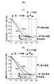
このような研磨過程の時間的な変化を図4を用いて説明する。簡単のため、上層金属と下層金属との2層からなる場合について述べる。第一の研磨においては、上層金属層は速やかに研磨される。そして、同図(a)の様に下層金属層の研磨速度が低い場合は下層金属層のほぼ表面で実質的に研磨が停止する。過剰研磨を行ってもほとんど影響はない。次に第二の研磨を行う。絶縁層の研磨速度は下層金属層の研磨速度よりも著しく低いために、研磨速度最低(Min)の部分の研磨が終了後、さらに10ないし20%程度の過剰研磨を行っても、深さばらつきを生じる最大部分の絶縁層の研磨量は極めてわずかである。その深さばらつきは研磨速度の比が大きいほど小さくなる。また、下層金属層の研磨速度も上層金属層の研磨速度と同程度である場合は、同図(b)の様にほとんど過剰研磨を行わずに絶縁層の表面で第一の研磨がほぼ終了させる。ここでは研磨速度が平均的な部分で研磨が終了した場合に第一の研磨を終了させても良い。研磨速度最大(Max)部分では絶縁層が若干研磨されるがその値は、上層もしくは下層の金属層の研磨速度の絶縁層の研磨速度に対する比にほぼ反比例して小さく抑制される。次に第二の研磨によって下層金属層を除去する。研磨速度最小(Min)部分の研磨終了から更に10ないし20%程度の過剰研磨を行っても良い。この場合、図5(a)の場合よりは若干深さばらつきが増すが、絶縁層の研磨速度が下層金属層の研磨速度よりも著しく低いために、従来技術によるよりは遥かにすくなくなる。著しい場合はディッシングやエロージョンを含めた深さばらつきは従来の1/3ないし1/5ていどにまで改善される。
【0017】
(2)また、第2に、上層の金属層の第1の研磨後、下層の金属層の第2の研磨の際に、下層金属層の研磨速度が上層金属層のエッチング速度よりも十分に大きくなる条件、具体的には5倍以上の条件で、研磨を行うことによって前記の目的が達成される。従来は、絶縁膜の研磨速度に対し、下層金属層の研磨速度を大きくするような研磨速度比を保つと、下層金属層表面が窪んでしまい、逆に平坦性が低下すると言われていた。これに対して、本発明では、研磨は、機械的作用に化学的作用が加味されて研磨される点に注目したものである。なお、機械的作用に化学的作用を加味した研磨においては、研磨とともに研磨剤に含まれる成分と金属層との化学反応による腐食(エッチングと記す)現象も多かれ少なかれ進行する。このエッチング速度の大小は研磨の精度に大きな影響を及ぼす。上層金属層のエッチング速度が大きい場合は、図3(e)に示したとおり、下層金属層32を研磨すると、上層金属層33が窪んでしまい、ダマシンで特に問題となっているディッシングやエロージョンを発生させてしまうからである。具体的には、下層の金属層の研磨速度の上層金属層のエッチング速度に対する比は5以上望ましくは10以上と、十分に大きく保つ事が必要である。さらに配線基板全面にわたって配線厚さを均一に保つ必要が生じた場合などは15以上が望ましい。
【0018】
(3)さらに、第3に、上層の金属層の第1の研磨の際、上層金属層のエッチング速度を上層の金属層の研磨速度の1/5以下、望ましくは1/10以下と低く保つようにし、その後下層金属層の第2の研磨を行うことによって達成される。このようにすることで、上層金属層の研磨の制御が容易となるとともに、下層金属層の除去を安定に行うことができる。勿論、この条件に加えて、下層金属層についても、上層金属層のエッチング速度が下層金属層の研磨速度の1/5以下、望ましくは1/10以下とすることが好ましい。
【0019】
前記の(2)または(3)に記載した方法では、第一もしくは第二の研磨の際に絶縁層が若干削られる可能性は残るが、研磨剤のpHは酸性であるため、研磨によって削られる量は極めて僅かである。なお、本明細書では、pHが6.5以上7.5以下を中性領域、6.5未満を酸性領域、7.5を超えた値を塩基性(アルカリ性)領域と呼ぶこととする。
【0020】
ここで、研磨速度のエッチング速度に対する比を大きくするには以下の方法がある。研磨速度は研磨剤の特性に加えて研磨荷重、研磨定盤の回転数の増加と共に増加する。一方、エッチング速度は研磨荷重などにはあまり依存せず、研磨剤の特性によってほぼ定まる。したがって、研磨荷重や定盤回転数の大きな条件を用いる事が望ましい。低い研磨荷重を用いるためには、それだけ研磨剤のエッチング速度を低減する事が必要になる。
【0021】
(4)第4に、絶縁膜の開口部内に埋め込まれた下層金属層の高さが、その開口部内の上層金属層の高さよりも高い半導体装置とすることによって達成される。このような構造であれば、上層金属層が側面の絶縁膜に直接接触する事がなくなり、信頼性向上に有利である。
【0022】
図2(d)には本発明によって形成した埋め込み配線の端部の詳細を示す。絶縁層21の金属層と接する面の上端部25は、研磨パッドとの摩擦によって若干の傾斜を有するが、その傾き角は1度以下である。また研磨で埋め込まれた上下金属層の端部24では、まず下層配線層21の研磨面が絶縁層21の研磨面と同等もしくは若干低くなっているが、その差は5nm以下である。さらに上層配線層23の研磨面は下層配線層の研磨面よりやはり5−10nm程度低くなっている。これは、下層金属層を研磨する際、上層金属層が銅であるため非常にエッチングされやすく、若干エッチングされてしまうためであると推定される。ただし、下層金属層から離れる方向の研磨面の傾きは1度以下と非常に高精度に形成できている。
【0023】
上記発明の構成は、以下の研磨の性質によるものである。
【0024】
発明者らは、研磨剤の組成を適切に選ぶことによって、基板温度を変更したりする必要なく当該研磨剤の研磨速度とエッチング速度とをほぼ独立に制御できる事を見いだした。これによって絶縁層の研磨速度を増すことなく、エロージョンやディッシング、さらには局所的窪み(局所的エロージョン)を著しく低減できる事がわかった。
【0025】
ここで研磨剤のエッチング速度の重要性について見いだされた事を述べる。一般にエッチング速度の測定は液が静止した状態で行われてきた(Static Etching Rateなどとも呼ばれる)。しかしながら、実際の研磨中には研磨剤が高速で配線基板表面を移動する。その速度は十ないし数十m/minに及ぶ。発明者らはこの様に液が高速で運動している状態でのエッチング速度は静止状態のエッチング速度の数倍にも増加する場合がある事を新たに見いだした。加えて、研磨すべき金属層が複数の層である場合、エッチング速度についてはそのすべてについて考慮しなければならない。ここでは上層、下層の2層の場合について説明するが、層数については2層に限るものではない。まず、上層金属層に対する第一の研磨ではその終了時に上層金属層と下層金属層との両方が配線基板表面に現れる。第一の研磨を過剰に行う事は一般に必要で、この際、上層金属層のディッシングを抑制するためには、上層金属層の研磨速度に対して上層金属層のエッチング速度を低く保つ事が必要である。その比率は5以上が必要で、望ましくは10以上が適している。
【0026】
下層金属層についてもディッシングを抑制するためには、上層金属層の研磨速度に対して下層金属層のエッチング速度を低く保つ事が望まれる。ただし、下層金属層が若干エッチングされてディッシングが生じたとしても、後述の第二の研磨終了後に保護層を形成するなどの手段を用いる場合はその限りではない。ただし、その場合はダマシン配線工程が複雑になる。これに対して、第二の研磨工程においては、上層および下層の金属層が共存する状態で研磨を開始し、配線基板平面部の下層金属層が除去されるまで継続される。従って第二の研磨剤については、下層の金属層の研磨速度が上層および下層の金属層の両方のエッチング速度よりも大きく保たれねばならない。その比はやはり5以上が必要で、10以上である事が望ましい。さらに配線抵抗の増加や面積が150mm径以上の大面積の配線基板全面での配線抵抗の均一性を高く保つためには15以上が望ましい。
【0027】
この様な研磨剤を用いれば、絶縁層との研磨速度の選択性を十分に大きく保っても研磨中に金属層の研磨面が窪むことは無視できる程度に小さく、結果としてエロージョンやディッシングの発生も抑制できる事がわかった。研磨剤が静止状態のエッチング速度と撹拌状態でのエッチング速度とはおおむね以下の様な比率が得られる。銅合金の様に化学反応性が強い金属では、従来はエッチング性の高い研磨剤が多かった。その様なエッチング性の高い研磨剤では静止状態でのエッチング速度が大きく、おおむね静止状態で5nm/minを越えることが多く、撹拌状態でのエッチング速度はその5ないし10倍にも達する。銅合金表面でのエッチング作用が強いために、研磨剤が撹拌されて常に新しい液が供給されるとエッチング速度が大幅に増加するものと考えられる。研磨剤を変えて、静止状態のエッチング速度を小さく、すなわちエッチング性を低くした場合、発明者らの実験ではおおむね5nm/minに達しない様な場合には、研磨剤を撹拌してもエッチング速度はたかだか2倍程度にしかならなかった。
【0028】
またチタンやタングステンもしくはその化合物などの場合は、化学反応性が相対的に低いために、撹拌状態のエッチング速度の静止状態のエッチング速度に対する比は2倍程度に留まる場合が多かったが、研磨速度も低くなるため、研磨速度の撹拌エッチング速度に対する比が重要で、おおむねこの比が10以上の場合は低エッチング性と判断できた。
【0029】
なお、本明細書で述べるエッチング速度とは、原則として運動状態を擬するために、液を撹拌しながら測定した値を指す。
【0030】
次に、図5に、本発明の一例として、第一の研磨および第二の研磨を実質的に同一の研磨剤を用い、銅の防食剤として用いたベンゾトリアゾル(BTA)の濃度を変化させる事のみによって第一の研磨剤および第二の研磨剤を得る方法について記す。まず、研磨速度やエッチング速度はBTAの濃度が増すに従って減少する。ただし、減少の度合いは研磨剤に含まれている有機酸の種類や濃度、もしくは酸化剤の濃度によって異なる。ただし、一般的にはBTAを添加していない状態での腐食性の強い研磨剤(高腐食性)の方がBTA添加による減少の度合いが顕著で、BTAを含まない場合の腐食性の低い研磨剤(低腐食性)の方が添加による減少の度合いが緩やかである場合が多い。所定の効果を得るに必要な濃度も異なる。便宜上、同図においてBTA濃度が1.0の相対濃度とは、銅合金の研磨速度が、BTAを加えない場合の研磨速度のほぼ10%以下になる濃度を表わしている。同図において高腐食性の研磨剤では第一の研磨剤はBTAの濃度が相対比0.01から0.3程度の範囲であれば良い。低腐食性研磨剤では、0.05程度から0.7程度となる。第二の研磨剤としてはBTAの濃度を第1の研磨の際の量よりも多くするように増やせば良い。なお、この研磨剤では下層金属層の研磨速度はBTAの濃度にあまり依存しないので、高濃度側では下層金属層の研磨速度が大きく、上層金属層や絶縁層の研磨速度の低い第二の研磨剤が得られる。ただし、下層金属層の研磨速度は金属や化合物の種類によって2ないし3倍程度変化することもあるので、適宜有機酸の種類の異なる研磨剤を選択する事が望ましい。
【0031】
第一の研磨剤として実質的に砥粒を含まない研磨剤を用いる場合は、下層金属層は殆ど研磨されない。この場合は絶縁層の研磨速度が低い事のみが重要であるので、図5における低濃度側、高濃度側のいずれの研磨剤をも第二の研磨剤として用いる事ができる。
【0032】
なお、研磨剤についての高腐食性、低腐食性の区別は一般化したものではない。本発明では、上層金属層用の第一の研磨剤について、静止状態での上層金属層のエッチング速度が5nm/min以下のものを低腐食性とした。
【0033】
次に、具体的な工程について、以下に示す。
【0034】
▲1▼第一の方法としては、第一の研磨の工程は上層のみならず下層の金属層も研磨される場合である。上層の金属層が銅合金である場合、上述の市販研磨剤のうちの過酸化水素を酸化剤として用いるものはほぼ全て適用できる。これらの研磨剤では、上層の金属層の研磨速度の下層金属層(タングステンやチタン、タンタルやそれらの合金)に対する研磨速度の割合は、おおむねプラスマイナス150%程度の範囲にある。また、概ね上層の金属層のエッチング速度は大きく、数十nm/minにも及ぶものも珍しくなく、上層金属層の研磨速度は上層金属膜のエッチング速度に対して3−5程度の比のものが多いため、必要に応じて防食剤の添加量を調整してエッチング速度を制御し、上層金属層のエッチング速度に対する上層金属層の研磨速度の比を5以上、望ましくは10以上に向上させる。但し、エッチング速度を下げすぎないようにし、スループットを向上させて、上層金属層の研磨時間を短縮させる。
【0035】
これらの上層および下層の金属層が共に研磨される研磨剤を用いた場合、第1の研磨では、過剰な研磨は避けることが望ましい。その反面、下層の金属層が部分的に残った状態で全体の研磨が終了したと誤認してしまうと、金属配線間が短絡してしまい、歩留まりを損なう。これも一段研磨法の短所である。そこで、過剰研磨をできるだけ少なくして第一の研磨工程を終了させ、引き続き第二の研磨を行う。ここでは、下層の金属層の研磨速度が絶縁層の研磨速度に比べて5倍よりも大きくなる様な第二の研磨剤を用いる事が必要である。過剰研磨を行った場合の絶縁層の膜厚減少を抑制するためである。研磨前の絶縁層の主表面が十分に平坦である場合には7倍以上、望ましくは10倍以上が適している。ただし、実際の配線基板上には数nmから100nm程度の深さの凹凸が残留している場合がある。この様な窪みに残留する金属層を除去するには研磨剤のエッチング性を増すか、絶縁層を削って平坦化するかのいずれかの方法がある。後者を用いる場合には、絶縁膜の研磨速度に対する下層の研磨速度の比を7倍乃至10倍程度で行うと、第二の研磨工程の研磨時間が短縮できる。なお、絶縁層の研磨速度と、上層金属層の研磨速度との関係は薄いが、過剰研磨の場合を考慮して、上層金属層の研磨速度の1/3より小さいことが望ましい。
【0036】
また、下層金属層を研磨するための第二の研磨剤による上層の金属層の研磨速度と下層の金属層の研磨速度との比は、上層金属層の研磨のための第一の研磨工程の条件や、配線基板表面の平坦性などに応じて調整すれば良い。
【0037】
以上、上層金属層及び下層金属層の研磨について説明したが、具体的には、上層金属層としては、例えば、銅もしくは銅を主成分とする合金、下層金属層としては、例えば、チタン、タンタル、タングステン、もしくはそれらの窒素や珪素との化合物を用いる。また、下層金属層は、必ずしも1層である必要はなく、2層以上の積層膜を用いても良い。なお、下層金属膜は、接着性や障壁性の面ではタンタル、チタンやその窒素化合物が優れているが、膜形成や研磨が容易という点でタングステンやその窒素化合物もしくは窒素珪素化合物などを用いても良い。
【0038】
ここで前記の第一の方法を可能にするための、所望の特性の研磨剤を実現する方法の例を挙げる。第一の研磨剤については、前述の市販研磨剤のうち、アルミナやシリカ砥粒、エッチング剤として過酸化水素水と有機酸を含むものに、微量の保護層形成剤を加えたものでよいがこれに限るものではない。市販研磨剤以外にさらに各種の有機酸や保護層形成剤を適宜添加したものを用いる事ができる。保護層形成剤としては、本発明ではベンゾトリアゾール(以下、BTAと記す)、BTAカルボン酸等のBTAの誘導体、ドデシルメルカプタン、トリアゾール、トリルトリアゾールおよびこれらの物質の誘導体又はそれらの混合物から選んで第一の保護層形成剤として用いた。これらの中でBTAが最も有効で、安定な効果が得られた。本発明では、研磨剤の種類にもよるが、おおむね0.01 wt%から0.05wt%程度を添加すれば十分であった。また、これらの保護剤の添加による研磨速度低下を避けるために、ポリアクリル酸、ポリメタクリル酸、もしくはこれらのアンモニウム塩またはそれらの混合物もしくはエチレンジアミン四酢酸から選んだ第二の保護層形成剤を必要に応じて添加した。これらを添加すると第一の保護層形成剤の濃度を低下させても良好な低エッチング特性を実現できるため、研磨速度の減少を抑制できる。研磨剤の種類にも依存するが、第一の研磨剤に含まれる第一の保護層形成剤の濃度が、0.01wt%以上0.05wt%以下の範囲で所望の特性が得られる。これらの方法により、上層の金属層について、研磨速度のエッチング速度に対する比は10以上を十分に確保できた。下地の絶縁層の研磨速度は研磨液のpHを弱酸性もしくは酸性に保ったために抑制できた。
【0039】
第二の研磨剤に要求される特性を実現するには、例えば第一の研磨剤と同一の市販研磨剤、もしくは種類の異なるその他の同一の市販研磨剤、もしくは上記の有機酸などを含む過酸化水素を酸化剤として用いる研磨剤であって良い。ただし、下層の金属層の研磨速度が上層金属層のエッチング速度よりも10倍以上大きなものを選ぶことが必要である。また、上層の金属層の研磨速度を下層の金属層のそれの150%以下に納めておく事が望ましい。第二の研磨剤に含まれる第一の保護層形成剤の濃度が0.04wt%以上1wt%以下となるように調整する。第一の研磨剤と同一研磨剤を用いる場合には、添加する第一の保護層形成剤の濃度を増せば良い。この場合には、上層金属層の研磨速度を下層金属層の研磨速度と同等以下に抑制することもできる。おおむね第一の研磨剤よりも0.01wt%以上増してやれば必要特性が得られる。例えば第一の研磨剤に添加した第一の保護層形成剤の濃度が0.04wt%であった場合、第二の研磨剤中の第一の保護層形成剤の濃度は0.05%以上とする。また、第一の研磨剤中の保護層形成剤の濃度が0.05wt%である場合には第二の研磨在中の保護層形成剤の濃度は0.06wt%以上が必要であった。保護層形成剤の濃度を更に増すと、下層の金属層の研磨速度は若干減少するが、上層の金属層の研磨・エッチング速度共に大幅に減少するので、加工形状精度の向上に着目した場合には更に適した特性となる。ただし、保護層形成剤には水に対する溶解度の低いものが多く、高濃度を溶解させることは技術的に難しい。実用レベルでは0.1wt%以上、最大1wt%程度添加すればどの研磨剤に対しても十分な低エッチング特性が得られた。
【0040】
ただし、以上の保護層形成剤添加の目的は第一の研磨剤に含まれる第一の保護層形成剤の濃度が、当該保護層形成剤を含まない場合の上層の金属層に対する研磨速度の95%以下40%以上の速度を保つ様に調整し、第一の研磨剤を用いて下層もしくは上層の金属層を研磨することを目的としているものであり、濃度の絶対値よりもこの研磨特性を実現する事の方が優先する。第二の研磨剤についてもそのpHは弱酸性もしくは酸性であったため、絶縁層の研磨速度は下層の金属層の研磨速度の1/5から1/10に抑制できた。研磨開始前の絶縁層表面の配線を形成すべきでない領域に深さ数nm以上で幅が10μm以下の様な窪みが存在する場合は、第二の研磨工程でこの絶縁層を研磨し、窪みを解消する必要がある。しかし、その様な研磨の障害となる窪みが所望の領域に存在しない場合には、第二の研磨剤に含まれる第一の保護層形成剤の濃度が、第一の保護層形成剤を含まない場合の上層の金属層の研磨速度の30%以下となる様に調整してあれば埋め込み配線の加工形状はより望ましい高精度を得られる。なお、第一もしくは第二の研磨剤共に主要成分が同一で、保護層形成剤が異なる場合は、第一の研磨剤による研磨の後、同一研磨定盤上でただちに第二の研磨剤を注いで研磨を行ったとしても、研磨剤が混じることによる悪影響は殆ど生じないという利点がある。なお、第二の研磨剤のpHは1以上6以下であると、絶縁膜の研磨速度を抑制して、下層金属層を選択的に研磨することが可能となる。
【0041】
また、第二番目の研磨工程を、無機の固体砥粒の濃度が0.1wt%以下と、実質的に砥粒を含まない研磨剤を用いて行う方法もある。第一の研磨工程に用いる研磨剤は上記の方法の場合と同等でよい。第二の研磨剤には、エッチング剤としての有機酸、酸化剤を含み、必要に応じて上層の金属層用の第一の保護層形成剤を添加する。有機酸としてはマロン酸、フマル酸、リンゴ酸、アジピン酸、安息香酸(例えば4−シアノ安息香酸)、フタル酸、尿酸、蓚酸、酒石酸、乳酸、コハク酸、クエン酸などの下層金属層表面に吸着されやすい酸、もしくはそれらのアンモニウムなどとの塩もしくは混合物から選ばれた少なくとも一者を含ませるのが良い。特にマロン酸、フタル酸、リンゴ酸、アジピン酸、もしくはそれらのアンモニウム塩が適しており、それぞれの濃度はおおむね0.1wt%以下で良い。また、必要に応じて、pH調整およびエッチング速度の調整のために、硝酸、硫酸、リン酸などの無機酸を加えても良い。この様に実質的に無機の固体砥粒を含まない研磨剤であっても下層の金属層を研磨して除去することができる。ただし、これらの酸を含んだ研磨剤では第一および第二のの金属層に対するエッチング速度は研磨速度の1/10以下にかろうじて保たれている程度である。このため、第一および上層の金属層のディッシングは上記の例よりも大きくなる。ただし、この様な第二の研磨剤を用いた場合、絶縁層の研磨速度は下層の金属層研磨速度の1/10よりはるかに小さくなり、絶縁層のエロージョンの増加は問題とならない。下層の金属層としてはタングステンもしくはタングステンを含む合金などが特に研磨速度が大きく、適している。
【0042】
▲2▼次に、第二の方法として、第一の研磨剤が絶縁層も下層の金属層も殆ど研磨せず、上層および下層の金属層をほぼ完全に独立した状態で研磨する方法について述べる。この様な第一の研磨剤の特性は、研磨剤中に含まれる無機の固体砥粒の濃度が0.1wt%以下と、実質的に無機の固体砥粒を含ませないことによって実現される。この様な砥粒を含まない研磨剤を用いると、所望の金属層は実用的な速度で研磨出来る反面で、下層の金属層や絶縁層の研磨速度は上層の金属層のそれの1/10以下となり、上層金属層の研磨は、下層の金属層もしくは絶縁層が露出した時点で実質的に停止する。十分に過剰研磨を行うことによって上層金属層の除去を完全なものとしても、下層金属層の少なくとも一部は残留する。
【0043】
下層金属層に対する第二の研磨研磨工程では、第一の方法で述べた第一の研磨剤もしくは第二の研磨剤のいずれかを第二の研磨剤として用いることが出来る。いずれを用いるにせよ、下層の金属層に対する研磨速度がその上層の金属層のエッチング速度よりも大きいことが必要である。具体的には、絶縁層の主平面が十分に平坦である場合には、下層の金属層の研磨速度は上層の金属層の研磨速度よりも3から5、望ましくは10以上であれば良い。ただし、深さ5nm以上でさまざまな大きさの窪み、たとえば幅が1ミクロン以下で長さが1ないし5ミクロン程度の傷状の窪みや、幅が5ミクロン以上で長さが10ミクロン以上にも及ぶ広くてなだらかな窪みなどが研磨前の絶縁層表面に存在する場合には、上記の比は0.5から3程度でも良い。窪みに相当する深さの絶縁層表面を研磨するためである。ただし、比が3以上であっても若干過剰な研磨を行えば下層の金属層は除去できる。この場合、処理能力が低下し、結果として研磨工程のコスト上昇を招くが、加工精度の面では問題ない。
【0044】
更に、第一、第二の研磨剤共に無機の固体砥粒が実質的に含まれていないものを用いる方法もある。第一の研磨剤は上記の実質的に無機の固体砥粒を含まない研磨剤を使用できる。第二の研磨剤はやはり前述の実質的に固体砥粒を含まない研磨剤を使用できる。それぞれの研磨特性や結果は上記のそれぞれの場合とほぼ同じである。この方法では、第二の研磨剤による下層の金属層に対する研磨速度が無機の固体砥粒を含む場合よりも小さく、またエッチング速度も増加する傾向にあるため、研磨速度のエッチング速度に対する比が低下する、またスループットもやや低下するという欠点を有する。ただし、両方の研磨剤共に無機の固体砥粒を実質的に含まないために、砥粒の沈殿に伴う研磨剤供給系や廃水系の配管のつまりなどの問題が発生しない、廃液処理が容易になる、などの利点があり、研磨工程全体としては大幅なコスト低減を図ることができる。また、実質的に砥粒を含まない研磨剤では絶縁層を殆ど研磨しないため、エロージョンの低減には有利である。
【0045】
なお、金属層の研磨の終点は公知の終点判定法を用いて検出できる。たとえば1996プロシーディングス・ファースト・インターナショナル・ケミカル−メカニカルポリッシュの256−262ページには光学的に研磨の終点を検知する方法が述べられている。下層の金属層と上層の金属層とでは光の反射率が異なるので、下層の金属層が露出した際に反射光の強度変化が検出できる。さらに研磨が進んで下層の金属層も研磨されて下地の絶縁層が露出すると光の反射強度の変化は一層顕著となる。なお、終点判定の方法としては研磨中の研磨定盤や基板ホルダを回転させるためのトルクの変化を検出する方法もある。砥粒を含まない研磨剤を用いた場合は、砥粒の機械的な摩擦の影響がほとんどなくなって、材料の違いによるトルク変化のみが現れるため、終点判定はより一層容易になる。
【0046】
なお、第一、上層の金属層の研磨においては、一般に配線基板全体にわたってプラスマイナス10%程度の研磨速度分布が存在する。従って終点判定装置を用いて研磨の終点判定を行ったとしても、配線基板の一部に研磨残りが生じる場合はあり得る。その様な場合は適宜それぞれの金属層対して第一、第二の研磨剤を用いた研磨を繰り返せば良い。
【0047】
さらに、以上に述べた第一および第二の研磨は研磨剤の特性が異なるために、それぞれ別個の研磨定盤を用いて行う事が望ましいことはいうまでもない。特に、第一および第二の研磨剤のいずれかが実質的に砥粒を含まず、他方が砥粒を含む場合には相互作用を避ける為に別定盤を用いる事が望ましい。ただし、同一定盤で行う事も可能である。第一の研磨剤中よりも第二の研磨剤中の方が上層金属層のための第一の保護層形成剤の濃度が高くなっているため、第二の研磨工程が悪影響を受ける事は少ない。ただし、引き続いて複数枚の配線基板を処理する場合は、保護層形成剤の濃度が高いと上層金属層の研磨が不安定になるので、前もって保護層形成剤の濃度を下げる処理、例えば純水や低濃度の保護層形成剤を含む液などを研磨パッド表面に注いだり、必要に応じてダイアモンドプレートやブラシなどによって研磨パッド表面から砥粒や保護層形成剤を除く操作などの処理を行う事が望ましい。本発明では上層金属層として銅合金の場合について述べたが、同様に化学反応性の強いアルミニウム合金に対しても同等の研磨条件を適用すると好結果が得られる。
【0048】
以上に述べたのは無機の固体砥粒を含む研磨剤もしくは実質的に無機固体砥粒を含まない研磨剤のいずれかを用いて、配線基板を樹脂の研磨パッドに押しつけて移動させながら研磨を行う方法である。これに対して、両者の中間的な方法として研磨パッド側に無機固体砥粒を含むシートを用いても良い。広義にはレジンボンド砥石(砥石と記す)に含まれるものである。これを表面に備えた回転定盤に配線基板を押しつけて研磨する。砥石を構成する砥粒としてはシリカ、アルミナもしくは酸化セリウム粉末を用いる。研磨剤としては酸化剤、有機酸および必要に応じて保護層形成剤を含む液を供給する。この液には無機固体砥粒は含まれていても含まれていなくとも良い。研磨を行うと砥石から適宜砥粒が遊離して配線基板の研磨効果を高める。樹脂のみの研磨パッドを使用する場合に比べて実質的に硬くなるため、平坦化効果が向上してディッシングを減らすことができる。ただし、砥粒が砥石中に固定されているため、研磨傷が発生しやすい。これを避けるために砥石には空孔率が高く、砥粒が遊離しやすい性質を付与する必要がある。
【0049】
【発明の実施の形態】
以下、本発明を図面を用いて具体的に説明する。
【0050】
(実施例1)
図1を用いて説明する。図1(a)はシリコンからなる配線基板10上に形成された酸化珪素からなる厚さ0.5ミクロンの絶縁層11に配線用の溝を形成し、下層の金属層12として厚さ50nmの窒化チタンの層を公知の反応性スパッタ法を用いて形成し、次いで上層の金属層13として厚さ800nmの銅層をスパッタ法によって形成し、熱処理によって溝中に埋め込んだ状態を示す。次いで図1(b)に示すように、第一の研磨剤を用いて上層の金属層14を研磨した。研磨剤としてはQCTT1010(ロデール社商品名)を7、30%過酸化水素水を3の割合で混合したものに対してBTAを0.01wt%添加して用いた。この研磨液は数%のアルミナ砥粒と、銅もしくは銅酸化物のエッチング剤として有機酸が含まれている。発泡ポリウレタンからなる格子溝入りの硬質研磨パッドを用いた。この時の研磨特性は研磨圧力が1平方センチメートル当たり200g、配線基板10と研磨定盤(図示せず)との相対速度が40m/minの条件下で約100nm/minであった。なおBTAを添加しない場合の研磨速度は約160nm/minであったので、添加によってほぼ60%に研磨速度は低下しているが、実用上は許容される。撹拌状態の上層金属層のエッチング速度は5nm/min以下であった。なお、より大きな研磨速度を得たい場合は、研磨圧力を大きくするなどの方法が知られている。この研磨は上層金属層13と下層金属層12をほぼ除去するに足る時間として10minを行った。ただし、絶縁層11表面全体を詳細に観察すると一部には下層の金属層の研磨残り12aも見られた。
【0051】
次に、第二の研磨定盤(図示せず)上に配線基板10を移動させて、図1(c)の様に下層金属層12およびその研磨残り12aの研磨を行った。研磨剤としてはQCTT1010を7、30%過酸化水素水を3の割合で混合したものを用い、これに0.1wt%のBTAを添加した。このBTA添加により銅合金の研磨速度は上記と同一条件下で20nm/min以下にまで減少した。その反面、窒化チタンの研磨速度は約50nm/minとBTA添加前と殆ど違いがなかった。この様な第二の研磨剤を用いて配線基板10を研磨すると、溝中の上層金属層13は殆ど研磨されず、溝以外の部分の下層の金属層の研磨残り12aを安定に除去することが出来た。下層の金属層に対して100%の過剰研磨を行っても上層の金属層のディッシング量の増加は30nm程度に留まり、埋込配線の断面積の減少は問題にならないほど少ない事がわかった。なお、第二の研磨剤に添加するBTAの濃度を変化させることにより、下層金属層に対する上層金属層の研磨速度の比を0.5から3の範囲で調整することができた。
【0052】
(実施例2)
図1を用いて説明する。実施例1と同等な配線基板10において、下層金属層12として50nm厚さのタングステンを用いている。膜形成にはスパッタ法を用いた。実施例1と第一の研磨剤および研磨条件を用い、上層金属層13を研磨して図1(b)の様に、下層金属層12がほぼ除去された状態とした。
【0053】
次に、第二の研磨定盤(図示せず)上に配線基板10を移動させて、図1(c)の様に下層金属層12およびその研磨残り12aの研磨を行った。第二の研磨剤としてはマロン酸およびBTAを0.1wt%と必要に応じて界面活性剤などを含む液を15、305過酸化水素水を1の割合で混合した液を用いた。固体砥粒は含まれていない。この研磨剤によれば、下層金属層12は約30nm/minの速度で研磨された。この時のエッチング速度は2.5−3nm/minであった。第二の研磨工程における絶縁層11の研磨速度は1nm/min以下であり、10minの過剰研磨によっても絶縁層11の表面の平坦性は殆ど劣化しなかった。また、この実施例では第一の研磨工程の後で配線基板10表面に付着している第一の研磨剤の砥粒を除去する効果も得られ、研磨終了後の異物は第二の研磨剤として砥粒入りのものを用いた場合より1/5以下の個数に減少するという効果も得られた。
【0054】
(実施例3)
実施例1および図1と同等の配線基板11と研磨剤とを用いるが、研磨定盤は下層の金属層12、上層の金属層13共に同一の研磨定盤を用いて行う場合について説明する。上層の金属層13の研磨を終える図1(b)の段階までは実施例1と同等であった。本実施例では配線基板11を移動させずに、研磨剤を第一の研磨剤から第二の研磨剤に変更して図1(c)の様に下層の金属層13である窒化チタンおよび窒化チタンの研磨を行った。この研磨において研磨剤の組成は保護層形成剤であるBTAの濃度を除いて同一であるため、両者が混じっても特に有害な問題は生じなかった。下層の金属層の研磨は実施例1と同等に安定に実施できた。
【0055】
ただし、次の配線基板を第一の研磨剤を用いて研磨を開始すると、研磨定盤には第二の研磨剤に含まれていた高濃度の保護層形成剤が残留しているため、上層の金属層の研磨速度が不安定になるという問題が生じた。そこで次の配線基板10の研磨に先立って研磨定盤に第一の研磨剤もしくは第一の研磨剤に含まれるのと同等以下の濃度のBTAを含む液を研磨定盤に注いでダイアモンド砥石を用いてコンディショニング(液を注ぎながら研磨パッド表面を削って整える処理)を行って研磨パッド表面に残留するアルミナ砥粒を除去した。この処理に要した時間は少なくとも10秒以上で20秒以上行うことが望ましかった。しかる後に次の配線基板に対して上層の金属層の研磨を開始したところ、前の配線基板10の研磨の影響を受けることなく、安定に第一、上層の金属層ともに不要部分が研磨除去され、埋込配線が良好に形成できた。
【0056】
(実施例4)
実施例2と同様の配線基板11を用いた。すなわち、下層金属層12として50nm厚さのタングステン膜を用いている。第一の研磨剤としては実施例1と同じ物を用いた。第二の研磨剤としては、保護層形成剤のBTAを1wt%含有させたキャボット社製のSS−W2000を体積15、30%濃度の過酸化水素水を体積1の割合で混合した物を用いた。第一の研磨剤による銅の研磨速度は実施例1と同等の条件下で約100nm/minであった。図1(b)の様に溝部以外において下層の金属層12を露出させた後、第二の研磨剤に変更して研磨を継続した。第二の研磨剤で上層の金属層14の研磨速度は20nm/minであったが、下層の金属層12の研磨速度は約150nm/min、下層金属層12の撹拌エッチング速度は10nm/min以下であった。第二の研磨剤による下層の金属層12の研磨の所要時間は1分以内であるが、研磨残りを生じさせないために過剰に2分間の研磨を行った。この過剰研磨によっても上層の金属層13の厚さは約15nmしか減少せず、十分な精度で埋め込み配線が形成された。
【0057】
(実施例5)
図2を用いて説明する。図2(a)は配線基板20上に形成された酸化珪素からなる厚さ0.5ミクロンの絶縁層21に配線用の溝を形成し、下層の金属層22として厚さ50nmの窒化タンタルの層を公知のスパッタ法を用いて形成し、次いで上層の金属層23として厚さ800nmの銅層をスパッタ法によって形成し、熱処理によって溝中に埋め込んだ状態を示す。次いで図1(b)に示すように、上層の金属層23を研磨し、溝以外の部分において下層の金属層12を露出させた。上層の金属層用研磨剤としては保護層形成剤として0.2wt%のBTAを、有機酸として0.15wt%のクエン酸を含むものを用いた。上層金属層13の研磨速度は、約100nm/minで上層金属層13の撹拌エッチング速度は8nm/minであった。無機の固体砥粒は加えていない。この第一の研磨工程において、下層金属層22は殆ど研磨されないため、配線基板20の全面にわたって残存していた。
【0058】
次に、第二の研磨定盤(図示せず)上に配線基板を移動させて、図1(c)の様に下層の金属層12の研磨を行った。研磨剤としては3wt%のアルミナ砥粒、フタル酸塩からなる有機酸を含む研磨剤と、30%過酸化水素水とを混合したものを用い、これに1wt%のBTAを添加した。このBTA添加により銅合金の研磨速度は実施例1と同一条件下で5nm/min以下にまで低下した。下層の金属層13の研磨速度は約20nm/minと低かったが、過剰研磨時間をも含めて4分間研磨したところ、溝中の上層の金属層13は殆ど研磨されず、溝以外の部分の下層の金属層である50nm厚さのタンタル層を安定に除去することが出来た。この時の絶縁層の研磨速度は3nm/min以下であった。
【0059】
なお、下層の金属層12として窒素を添加しながら用いる反応性スパッタ法を用いてタンタル膜を形成すると窒化タンタル膜が形成できる。この膜に対する研磨速度は約30nm/minとやや研磨が容易であった。
【0060】
(実施例6)
図2を用いて説明する。実施例2と同等の配線基板20を用いた。この配線基板20に対して、第一の研磨剤としては第一の保護層形成剤として0.1wt%のBTA、第二の保護層形成剤として0.05wt%のポリアクリル酸アンモニウムを、有機酸として0.05wt%のリンゴ酸を含むものを用いた。上層金属層13の研磨速度は、約150nm/minで上層金属層13の撹拌エッチング速度は5nm/minであった。無機の固体砥粒は加えていない。この研磨によって図1(b)に示すように、上層の金属層23を研磨し、溝以外の部分において下層の金属層12を露出させた。この際、50%相当の過剰研磨を行ったが、下層金属層22は残存しており、上層金属層13の窪みは数nm以下に抑制されていた。
【0061】
次に、第二の研磨定盤(図示せず)上に配線基板20を移動させて、図2(c)の様に下層金属層22の研磨を行った。第二の研磨剤としてはマロン酸およびBTAを0.1wt%と必要に応じて界面活性剤などを含む液を15、305過酸化水素水を1の割合で混合した液を用いた。固体砥粒は含まれていない。この研磨剤によれば、下層金属層22は約30nm/minの速度で研磨された。この時のエッチング速度は2.5−3nm/minであった。第二の研磨工程における絶縁層21の研磨速度は1nm/min以下であり、10minの過剰研磨によっても絶縁層21の表面の平坦性は殆ど劣化しなかった。また、この実施例では第一の研磨、第二の研磨の工程共に砥粒を含まない研磨剤を用いたため、研磨後の残留異物は砥粒を含む研磨剤を用いた場合の1/10以下に改善されていた。
【0062】
(実施例7)
図1を用いて説明する。実施例1と同等の配線基板試料を用い、上層金属層13までを形成した。研磨装置の回転定盤にはシリカ砥粒を用いたレジンボンド砥石(図示せず)を研磨パッドの代わりに設置した。シリカ砥粒の粒子サイズは0.4ミクロンプラスマイナス0.2ミクロンのものが80%以上を占める様に揃ったものを用いた。砥石は多孔質の脆い構造とした。砥粒の固定にはノボラック系樹脂を用い、空孔率は約30%であった。次いで図1(b)に示すように、配線基板10を回転するレジンボンド砥石に押しつけて研磨を行った。研磨条件はこれまでと同等であるが、研磨傷の発生を避けるため、平方センチメートル当たり140gと小さくした。第一の研磨剤としては有機酸としてクエン酸を、保護層形成剤としてBTAを0.2wt%含む液を供給した。その結果、上層金属層13は無機固体砥粒を含む従来の研磨剤とほぼ同等の研磨速度で除去できた。研磨速度はほぼ120nm/minであった。エッチング速度は約3nm/minであった。約10%の過剰研磨を加えて7min30secの研磨を行った。砥石は硬いためにこの研磨によって1mm角の領域でも上層金属層13は除去できた。ただし、配線基板10上にはかなりの領域で下層金属層の研磨残り12aが見られた。
【0063】
次に同一の砥石上で第二の研磨剤として、第一の研磨剤中のBTAを0.5wt%に増したものを用いた。このBTA濃度のもとでは上層金属層13の研磨速度は10nm/min以下となった。一方、下層金属層12の研磨速度は約50nm/min、そのエッチング速度は2nm/min以下であった。2.5minの研磨によりパターンの無い領域でも下層金属層12の研磨残りは観察されなかった。この砥石を用いる方法は広い幅の溝部分に対してもディッシング少なく埋め込み配線を形成できる点にある。同一研磨荷重を用いた場合は約3倍の幅広いパターンに対してもほぼ同等ディッシングに抑制できた。
【0064】
引き続き別の配線基板を研磨する場合に備え、砥石に純水を注ぎながらコンディショニングを行い、砥石表面のBTAの残留濃度を低下させた。
【0065】
(実施例8)
図6乃至図11を用いて、デバイスを有する配線基板上に二層の銅配線を形成する場合について述べる。なお本実施例では、デバイスとしてトランジスタを形成した場合を示すが、ダイナミックランダムアクセスメモリなどの場合はキャパシタを形成する工程が加わるだけで、素子から電極を引き出す工程以降は実質的に同等である。
【0066】
まず、図6ではp型不純物を含むシリコン基板からなる配線基板610表面に、デバイス相互の分離のための埋め込み絶縁層611を形成する。この表面をシリカ砥粒とアンモニアとを含むアルカリ性研磨剤を用いた研磨によって平坦化してある。次にn型不純物の拡散層612をイオン打ち込みや熱処理等を用いて形成し、ゲート絶縁膜613を熱酸化法などによって形成する。次に多結晶シリコンや高融点金属と多結晶シリコンとの積層膜などからなるゲート614を加工して形成する。その表面には酸化珪素もしくはリンを添加した酸化珪素膜などからなるデバイス用保護膜615と外部からの汚染物質の侵入を防ぐための、窒化珪素膜などからなる汚染防止膜616を被着する。さらにテトラエトキシシラン(TEOSと記す)を原料として用いたプラズマ化学気相成長法(プラズマCVD法と記す)によって形成した酸化珪素(p−TEOSと記す)からなる平坦化層617を約1.5ミクロンの厚さに形成した後上記の絶縁膜用の研磨によって約0.8ミクロンの厚さを削って表面を平坦化した。さらにその表面を銅拡散の防止のための窒化珪素からなる第二の保護層618によって被覆する。引き続いて所定の部分にデバイスとの接続用のコンタクト孔619を開口し、接着と汚染防止とを兼ねたチタンと窒化チタンの積層膜620とタングステンの層621を形成して、孔以外の部分を研磨によって除去していわゆるプラグ構造を形成する。チタンや窒化チタンの層は反応性スパッタ法やプラズマCVD法によって形成する。タングステンもスパッタ法やCVD法を用いて形成できる。ここでコンタクト孔の大きさはおおむね直径が0.25ミクロン以下で、深さは0.8ないし0.9ミクロンであった。なお、上記のダイナミックランダムアクセスメモリ等のための素子を形成する場合にはこの深さは更に増して、1ミクロン以上にも達する場合もある。積層膜620の厚さは平面部で約50nmとした。タングステンの層621の厚さは約0.6ミクロンとした。コンタクト孔を十分に埋め込み、かつ膜表面の平坦性を改善してタングステンの研磨を容易にする為である。なお、このタングステンおよび積層膜の研磨には前述の市販の研磨剤を用いても良いし、本発明の第二の研磨剤を用いても良い。
【0067】
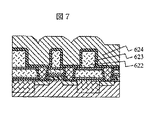
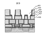
次に図7の様に第一の層間絶縁層622を形成し、配線用の溝を形成して、窒化チタンからなる厚さ50nmの第一の下層金属層623と第一の上層金属層624として銅膜を形成した。ここで第一の層間絶縁膜622の厚さは0.5ミクロンとした。なお、溝の形成は公知の反応性ドライエッチング技術を用いたが、第二の保護層618はエッチングのストッパの役割も果たした。窒化珪素のエッチング速度は酸化珪素のそれのほぼ1/5であるので、厚さは約10nmとしている。第一の上層金属層624としては0.7ミクロン厚さの銅をスパッタ法によって形成し、約450度の熱処理を施して流動させ、溝の中に埋め込んだ。次いで第一の上層金属層624および第一の下層金属層623は本発明の方法によって研磨した。研磨後の表面に窒化珪素からなる第二の汚染保護層625をプラズマCVD法によって形成した。この層の厚さは20nmとした。第一の研磨剤としては有機酸と保護層形成剤、酸化剤を含み無機の固体砥粒は含まない研磨剤を用いた。第一の研磨では研磨圧力を増加させて平方センチメートル当たり300gにまですることによって、研磨速度は約200nm/minにまで増加したが、第一の下層金属層623の研磨速度はその1/10以下であり、その表面で研磨は停止した。第二の研磨においては図5に示したBTAが低濃度領域の低腐食性のアルミナ砥粒入り研磨剤を用いた。BTAの相対濃度は0.1から0.2の範囲で、研磨圧力が平方センチメートル当たり200gの場合、第一の下層金属層623の研磨速度は約70nm/minであった。この研磨剤では銅の研磨速度は大きいが、エッチング速度は十分に低い。また、本実施例の様に配線基板610表面に多様なデバイスが形成され、それに伴って大きくかつ複雑な表面段差が生じてしまう場合には、平坦化層617を研磨してあっても第一の層間絶縁層622表面は十分には平坦化されず、深さ5nm程度で幅がデバイスの幅たとえば5ミクロン程度の浅くて広い窪みなどが残る場合がある。第一の研磨剤の特性が極めて優れており、ディッシングなどが殆ど生じない場合にはこのような浅い窪みにも第一の上層金属層624の研磨残りを生じる場合がある。本実施例で第一の上層金属層の研磨速度の比較的大きな、BTAが低濃度領域の研磨剤を第二の研磨剤として用いたのは、このような研磨残りによる配線短絡を防ぐためである。次に第二の層間絶縁膜626として厚さ0.7ミクロンのp−TEOS膜を形成し、その表面を0.2ミクロン深さに上記の方法によって研磨して平坦化した。この平坦化は下層の第一の上層金属層625の研磨工程などで生じた段差を解消させるためである。次に第三の汚染防止層627として厚さ0.2ミクロンのプラズマCVD窒化珪素膜を、第三の層間絶縁膜628として厚さ0.7ミクロンのp−TEOS膜を形成した。次に第一の層間接続用孔629および第二の配線用の溝630を公知のフォトリソグラフィ技術と反応性ドライエッチングとを用いて形成し、第一の上層金属層624表面を露出させる。このような二段構造の溝パターンを形成する際、窒化珪素膜627はエッチングのストッパとして働く。こうして形成した二段構造の溝に第二の下層金属層として50nm厚さのチッ化チタン膜631をプラズマCVD法によって図8、図9の様に形成した。
【0068】
さらに図10の様に第二の上層金属層632をスパッタ法によって厚さ1.2ミクロンに形成し、450℃の熱処理によって埋め込んだ。研磨を行い、第二の上層金属層632および第二の下層金属層631を研磨して図11の銅の2層配線を形成した。研磨すべき第二の上層金属層632が厚いために、ここでは保護層形成剤の濃度の低い、図5に示したアルミナ砥粒を含み、BTAが低濃度の低腐食性研磨剤を用いて第二の上層金属層632を研磨した。研磨速度は約200nm/minとなる条件を用い、研磨時間は過剰研磨も含めて8分とした。第二の研磨剤としては、同じく低腐食性の研磨剤にBTAを高濃度に添加したものを用いた。BTA濃度の相対比は約0.7で、下層金属層631の研磨速度の方が上層金属層の研磨速度よりも大きい。以上に述べた様に、二段に渡る研磨法を用いると、各々の絶縁膜や金属層の表面の平坦性を良好に保ちながら、高い歩留まりで多層の配線を形成できる。
【0069】
(実施例9)
ダマシンによる配線が上層金属層と二層の下層金属層との実質三層からなる場合について図12を用いて説明する。同図(a)は表面に所定の絶縁層(図示せず)が形成されているシリコンからなる配線基板720上に絶縁層71としてp−TEOS膜を厚さ0.5ミクロンに形成し、さらに溝を開口した上に、接着用下層金属層72aとして厚さ3nmのチタンを、さらにバリア用の下層金属層72bとして厚さ40nmの窒化チタン膜を反応性スパッタ法によって形成、引き続いて上層金属層73として厚さ0.8ミクロンの銅を形成し、熱処理によって埋め込んだ状態を示す。次に砥粒を含まない第一の研磨剤を用いて上層金属層73を研磨して下層金属層72bを同図(b)の様に露出させた。次いでアルミナ砥粒と有機酸および過酸化水素を含む研磨剤に図5における保護層形成剤として相対濃度0.8に相当するBTAカルボン酸を添加したものを用いて研磨した。上層金属層73の研磨速度は、添加しない場合の20%以下に低下している。この研磨剤によって下層金属層72bは約80nm/minと高速で研磨されたが、接着用下層金属層72aの研磨速度は約20nm/minと低かった。ただし、接着用下層金属層72aの厚さは3nmと薄いために、下層金属層72a、72b両方を合わせた平均の研磨速度は約70nm/minと十分に高い値を示した。なお、絶縁層71の研磨速度は約5nm/minであった。
【0070】
なお、以上の実施例1から9においては上層金属層の形成法としてはスパッタ法を用いて熱処理によって溝内に埋め込んだ。この場合、埋め込み特性は十分でないために、0.5ミクロン深さの溝に対して、0.8ミクロン厚さの上層金属層を形成する必要があった。したがって、その研磨0.8ミクロン厚さに対して行い、過剰研磨もそれに対して10%以上行う必要があった。加えて、溝のアスペクト比が3を越える様な場合は埋め込みが十分に行われないという問題があった。これに対して、硫酸銅を主成分とする液を用いて電気メッキによって埋め込んだ配線基板についても検討した。埋込性はスパッタ法よりも大幅に改善され、深さ0.5ミクロンの溝に対して、形成する膜厚は0.6ミクロンで十分であった。ただし、接着性の改善などのために、研磨に先立った窒素中で350度30minの熱処理を行った。この様な配線基板に対して本発明の研磨を実施したところ、第一の研磨において、スパッタ法によって形成した膜に比べておおむね5−10%程度研磨速度が増加した以外には殆ど違いが見られず、良好な平坦性を得た。
【0071】
なお、本発明の適用により、ディッシングとエロージョンを加えた窪みの大きさは、従来法による場合の約1/2に低減できた。第一、第二の研磨剤のいずれか片方もしくは両方に固体砥粒を含まない研磨剤を用いた場合は特に改善が顕著で窪みの深さは1/3以下に低減された。
【0072】
【発明の効果】
本発明によって、下層の金属層の研磨残りを生じることなく、上層金属のディッシングや絶縁層のエロージョンも低減させて高精度の埋め込み配線が形成できる。特に研磨前の絶縁層の表面が十分に平坦な場合には、第二の研磨剤に第一の保護層形成剤を十分に高い濃度に添加して、上層金属層を殆ど研磨しない特性を付与して用いることが出来る。この場合、第二の研磨工程において研磨荷重が溝パターン分布を殆ど示さなくなるために、配線基板の所望領域全体にわたって殆どディッシングやエロージョンのない平坦な表面を実現できる。この時のディッシングやエロージョンの深さは従来技術の1/5以下となる。
【図面の簡単な説明】
【図1】上層金属層に加えて下層金属層も研磨できる研磨剤を用いてダマシン配線を形成するための工程を示す図。
【図2】下層金属層を殆ど研磨しない研磨剤を用いてダマシン配線を形成するための工程を示す図。
【図3】従来のダマシン配線形成プロセスの課題を示す図。
【図4】本発明の研磨法における配線基板表面の深さ方向の時間変化を示す図。
【図5】本発明の研磨剤の例を示す図。
【図6】デバイスを形成した配線基板上に2層の銅配線を形成した例を示す図。
【図7】デバイスを形成した配線基板上に2層の銅配線を形成した例を示す図。
【図8】デバイスを形成した配線基板上に2層の銅配線を形成した例を示す図。
【図9】デバイスを形成した配線基板上に2層の銅配線を形成した例を示す図。
【図10】デバイスを形成した配線基板上に2層の銅配線を形成した例を示す図。
【図11】デバイスを形成した配線基板上に2層の銅配線を形成した例を示す図。
【図12】下層金属層が2層の積層膜からなる場合を示す図。
【符号の説明】
10、20、30、70…配線基板
11、21、31、71…絶縁層
12、22、32…下層金属層
13、23、33、73…上層の金属層
12a、22a…下層金属層の研磨残り
33a…上層金属層の研磨残り
72a…接着用下層金属層
72b…バリア用の下層金属層
610…配線基板
611…埋め込み絶縁層
612…拡散層
613…ゲート絶縁膜
614…ゲート
615…デバイス用保護膜
616…汚染防止膜
617…平坦化層
618…第二の保護層
619…コンタクト孔
620…積層膜
621…タングステンの層
622…第一の層間絶縁層
623…第一の下層金属層
624…第一の上層金属層
625…第二の汚染防止層
626…第二の層間絶縁膜
627…第三の汚染防止層
628…第三の層間絶縁層
629…第一の層間接続孔。[0001]
BACKGROUND OF THE INVENTION
The present invention relates to a method of manufacturing a semiconductor device and a semiconductor device, and more particularly to a method of forming metal wiring of a semiconductor device using polishing and a semiconductor device manufactured using the method.
[0002]
[Prior art]
In recent years, flattening of the surface of a wiring board has been regarded as important for semiconductor integrated circuits (hereinafter referred to as LSI). Chemical mechanical polishing (CMP; hereinafter referred to as polishing unless otherwise specified) is one of the representative techniques. For example, US Pat. No. 4,944,836. For example, a metal film for wiring is formed on a silicon substrate or the like (hereinafter referred to as a wiring substrate) on which LSI is formed, and this is performed using a known lithography technique and reactive dry etching (referred to as RIE). A wiring pattern is processed, and an insulating layer is formed thereon. When the surface of the insulating layer is flattened by polishing, it is effective for improving the processing accuracy of the wiring formed in the upper layer.
[0003]
On the other hand, a metal wiring forming method using polishing called a damascene method is also attracting attention. In the damascene method, an insulating film is formed on a wiring substrate, and a groove having a reverse pattern of wiring is formed on the insulating film using a known lithography technique and RIE. A metal film for wiring is deposited thereon, and the metal film other than the portion embedded in the trench is removed by polishing to form a buried wiring. This technique is disclosed, for example, in JP-A-2-278822. This method is particularly effective when a copper alloy, which is difficult to be finely processed by RIE, is used as a wiring, but is also being studied for miniaturization of an aluminum wiring pattern.
[0004]
Details of the conventional damascene method are introduced in Japanese Patent Application Laid-Open No. 10-214834 and pages 415-422 of the Proceedings CMP MCI Conference published in 1997. In these examples, a composite layer of tungsten and titanium is described. Based on these, description will be made with reference to FIG. First, an
[0005]
Next, the
[0006]
The cause of the occurrence of such a step is explained as follows. In the case of a metal abrasive, the polishing rate generally decreases in the order of upper metal layer-lower metal layer-insulating layer. In particular, the difference in polishing rate between the lower metal layer and the insulating layer is large, and the polishing rate of the insulating layer often reaches only a few tenths of the polishing rate of the lower metal layer. Since the polishing speed of the upper and
[0007]
As a method for proposing a step as described above, a two-step polishing method that effectively reduces the difference in polishing rate has been proposed. That is, the polishing is finished first when the polishing of the
[0008]
Further, the polishing of copper alloys is introduced in JP-A-8-83780. Here, a method of polishing a copper alloy and tungsten film is described. As an abrasive, it is stated that an alumina abrasive grain, a metal layer containing an oxidizing agent, an etching agent, and an anticorrosive agent exhibit good characteristics. That is, the basic polishing mechanism is to mechanically remove the oxide by friction with inorganic abrasive grains or a polishing pad while oxidizing the metal surface with an oxidizing agent. An etchant is used to increase the polishing rate of the metal layer. However, when an etching agent is added, etching also proceeds on the metal film in the groove portion where the abrasive grains and the polishing pad do not contact, and flattening is impaired. In order to avoid this, an anticorrosive agent is added. By increasing the ratio between the polishing rate and the etching rate, dishing can be suppressed, and as a result, the processing accuracy can be improved. In this example, the pH of the abrasive is considered to be almost neutral. However, when an anticorrosive agent is added, the polishing rate also decreases rapidly. When 0.1% of the anticorrosive agent is added, the polishing rate is reduced to about 10 nm / min. Therefore, the ratio between the polishing rate and the etching rate does not necessarily increase as the concentration of the anticorrosive increases. Moreover, since a polishing rate of about 100 nm / min is necessary for practical use, such characteristics are not suitable for actual use. In order to further reduce dishing, the copper alloy is polished at room temperature, and then the barrier layer is polished by changing the polishing characteristics by lowering the temperature of the polishing platen and the polishing agent. A two-step polishing method is also introduced.
[0009]
The following are known as commercial abrasives for performing these polishings. As a polishing agent for copper alloy, there is QCTT1010 (trade name of Rodel, Inc. used by mixing with hydrogen peroxide) containing alumina abrasive grains. As an abrasive for tungsten, SS-W2000 containing silica abrasive grains (trade name of Cabot Corporation. Used in combination with hydrogen peroxide solution), WA-400 containing alumina abrasive grains (trade name of Cabot Corporation. Used in combination with FE-400 solution containing ferric nitrate), MSW-1000 (trade name of Rodel Co., Ltd. and used in combination with hydrogen peroxide solution), XGB-5542 (trade name of Rodale Co., Ltd., potassium oxide) Used in combination). In order to increase the polishing rate of the insulating film, it is desirable that the abrasive is alkaline, and generally an abrasive containing silica abrasive grains and ammonium hydroxide or potassium hydroxide is used. Insulating films have been polished for a long time, and many products are commercially available. It is known that the hydrogen ion concentration (denoted as pH) of the liquid changes depending on the concentration of ammonium hydroxide or potassium hydroxide, and the polishing characteristics also change. In the above-mentioned Japanese Patent Application Laid-Open No. 10-214834, it is considered that this type of abrasive is also used for polishing a titanium layer which is a lower metal layer.
[0010]
[Problems to be solved by the present invention]
However, in this two-stage polishing method, as explained in FIG. 3, in order to make the polishing rate of the
[0011]
In addition, the polishing rate of titanium, which is the
[0012]
In order to form the low resistance wiring uniformly over the entire surface of the wiring substrate, the upper layer is formed over a predetermined portion of the entire surface of the wiring substrate, for example, the region where the wiring circuit element is formed, without reducing the thickness of the insulating
[0013]
The present invention has been made in view of the above points, and suppresses the deterioration of the wiring shape when forming a laminated damascene wiring composed of an upper metal layer and a lower metal layer having a barrier effect, while reducing yield and An object is to form the wiring by removing the first alloy layer with good stability.
[0014]
The above-mentioned Japanese Patent Application Laid-Open No. 10-214834 has no description on chemical etching for polishing, and it is unclear how much chemical etching has progressed in the polishing process.
[0015]
[Means for Solving the Problems]
(1) First, when the second metal layer is polished second after the first polishing of the upper metal layer, the lower metal film has a lower polishing rate than the lower insulating layer. It is achieved by polishing to be larger than the above. That is, when the second polishing for polishing the
[0016]
Such a temporal change in the polishing process will be described with reference to FIG. For the sake of simplicity, the case of two layers of an upper layer metal and a lower layer metal will be described. In the first polishing, the upper metal layer is quickly polished. Then, when the polishing rate of the lower metal layer is low as shown in FIG. 5A, the polishing is substantially stopped at the almost surface of the lower metal layer. Even if the excessive polishing is performed, there is almost no influence. Next, a second polishing is performed. Since the polishing rate of the insulating layer is significantly lower than the polishing rate of the lower metal layer, even if excessive polishing of about 10 to 20% is performed after the polishing of the portion with the lowest polishing rate (Min) is completed, the depth variation The amount of polishing of the maximum portion of the insulating layer that causes the problem is extremely small. The depth variation decreases as the polishing rate ratio increases. In addition, when the polishing rate of the lower metal layer is about the same as the polishing rate of the upper metal layer, the first polishing is almost completed on the surface of the insulating layer without performing excessive polishing as shown in FIG. Let Here, the first polishing may be terminated when the polishing is completed at an average polishing rate. At the maximum polishing rate (Max) portion, the insulating layer is slightly polished, but the value is suppressed to be almost in inverse proportion to the ratio of the polishing rate of the upper or lower metal layer to the polishing rate of the insulating layer. Next, the lower metal layer is removed by second polishing. An excessive polishing of about 10 to 20% may be performed after the polishing of the minimum polishing rate (Min) portion is completed. In this case, although the depth variation slightly increases as compared with the case of FIG. 5A, the polishing rate of the insulating layer is remarkably lower than the polishing rate of the lower metal layer, so that it is much less than in the prior art. In a remarkable case, the depth variation including dishing and erosion is improved to 1/3 to 1/5 of the conventional one.
[0017]
(2) Second, after the first polishing of the upper metal layer, the polishing rate of the lower metal layer is sufficiently higher than the etching rate of the upper metal layer during the second polishing of the lower metal layer. The above-mentioned object is achieved by performing polishing under conditions of increasing, specifically, conditions of 5 times or more. Conventionally, it has been said that when the polishing rate ratio that increases the polishing rate of the lower metal layer with respect to the polishing rate of the insulating film is maintained, the surface of the lower metal layer is depressed, and conversely, the flatness is lowered. On the other hand, in the present invention, the polishing is focused on polishing by adding a chemical action to a mechanical action. In polishing with a chemical action in addition to a mechanical action, corrosion (denoted as etching) due to a chemical reaction between a component contained in the abrasive and the metal layer progresses to a greater or lesser extent. The magnitude of this etching rate has a great influence on the polishing accuracy. When the etching rate of the upper metal layer is high, as shown in FIG. 3E, when the
[0018]
(3) Third, at the time of the first polishing of the upper metal layer, the etching rate of the upper metal layer is kept as low as 1/5 or less, preferably 1/10 or less of the polishing rate of the upper metal layer. And then by performing a second polishing of the underlying metal layer. By doing so, polishing of the upper metal layer can be easily controlled and the lower metal layer can be removed stably. Of course, in addition to this condition, also for the lower metal layer, the etching rate of the upper metal layer is preferably 1/5 or less, more preferably 1/10 or less of the polishing rate of the lower metal layer.
[0019]
In the method described in the above (2) or (3), there is a possibility that the insulating layer is slightly scraped during the first or second polishing, but the pH of the polishing agent is acidic, so that the polishing is performed by polishing. The amount produced is very small. In the present specification, a pH of 6.5 to 7.5 is referred to as a neutral region, a pH less than 6.5 is referred to as an acidic region, and a value exceeding 7.5 is referred to as a basic (alkaline) region.
[0020]
Here, there are the following methods for increasing the ratio of the polishing rate to the etching rate. In addition to the characteristics of the abrasive, the polishing rate increases as the polishing load and the rotation speed of the polishing platen increase. On the other hand, the etching rate does not depend much on the polishing load and is substantially determined by the characteristics of the abrasive. Therefore, it is desirable to use conditions with a large polishing load and surface plate rotation speed. In order to use a low polishing load, it is necessary to reduce the etching rate of the abrasive.
[0021]
(4) Fourth, this is achieved by making the semiconductor device in which the height of the lower metal layer embedded in the opening of the insulating film is higher than the height of the upper metal layer in the opening. With such a structure, the upper metal layer is not in direct contact with the side insulating film, which is advantageous in improving reliability.
[0022]
FIG. 2D shows details of the end portion of the buried wiring formed according to the present invention. The
[0023]
The structure of the said invention is based on the property of the following grinding | polishing.
[0024]
The inventors have found that by properly selecting the composition of the abrasive, the polishing rate and the etching rate of the abrasive can be controlled almost independently without having to change the substrate temperature. As a result, it has been found that erosion, dishing, and local depression (local erosion) can be significantly reduced without increasing the polishing rate of the insulating layer.
[0025]
Here, it is described that the importance of the etching rate of the abrasive was found. In general, the measurement of the etching rate has been performed in a state where the solution is stationary (also called a static etching rate). However, during actual polishing, the abrasive moves on the surface of the wiring board at a high speed. The speed ranges from 10 to several tens of m / min. The inventors have newly found that the etching rate when the liquid is moving at high speed may increase several times as much as the etching rate in the stationary state. In addition, when the metal layer to be polished is a plurality of layers, all of the etching rates must be considered. Here, the case of two layers, the upper layer and the lower layer, will be described, but the number of layers is not limited to two. First, in the first polishing for the upper metal layer, both the upper metal layer and the lower metal layer appear on the surface of the wiring board at the end of the polishing. It is generally necessary to perform the first polishing excessively. At this time, in order to suppress dishing of the upper metal layer, it is necessary to keep the etching rate of the upper metal layer lower than the polishing rate of the upper metal layer. It is. The ratio needs to be 5 or more, preferably 10 or more.
[0026]
In order to suppress dishing for the lower metal layer as well, it is desirable to keep the etching rate of the lower metal layer lower than the polishing rate of the upper metal layer. However, even if the lower metal layer is slightly etched and dishing occurs, this is not the case when a means such as forming a protective layer after the second polishing described below is used. However, in this case, the damascene wiring process becomes complicated. On the other hand, in the second polishing step, polishing is started in the state where the upper layer and the lower layer metal layer coexist, and is continued until the lower layer metal layer on the plane portion of the wiring board is removed. Therefore, for the second abrasive, the polishing rate of the lower metal layer must be kept higher than the etching rate of both the upper and lower metal layers. The ratio needs to be 5 or more, and is preferably 10 or more. Furthermore, 15 or more is desirable in order to maintain high uniformity of wiring resistance over the entire surface of a large-sized wiring board having an area of 150 mm or more in diameter and increasing wiring resistance.
[0027]
When such an abrasive is used, it is negligibly small that the polished surface of the metal layer is recessed during polishing even if the selectivity of the polishing rate with the insulating layer is kept sufficiently large, resulting in erosion and dishing. It was found that the occurrence can be suppressed. The following ratios are generally obtained between the etching rate when the abrasive is stationary and the etching rate when the abrasive is stirred. In the case of a metal having a strong chemical reactivity such as a copper alloy, conventionally, there are many abrasives with high etching properties. Such an abrasive having a high etching property has a high etching rate in a stationary state and generally exceeds 5 nm / min in a stationary state, and the etching rate in a stirring state reaches 5 to 10 times that. Since the etching action on the surface of the copper alloy is strong, it is considered that the etching rate is greatly increased when the abrasive is stirred and a new liquid is constantly supplied. When the polishing agent is changed to lower the etching rate in a stationary state, that is, the etching property is low, in the case where the inventors do not reach 5 nm / min. It was only about twice as much.
[0028]
In the case of titanium, tungsten, or a compound thereof, since the chemical reactivity is relatively low, the ratio of the etching rate in the stirring state to the etching rate in the stationary state often remains about twice, but the polishing rate Therefore, the ratio of the polishing rate to the stirring etching rate is important. When this ratio is approximately 10 or more, it can be determined that the etching rate is low.
[0029]
The etching rate described in this specification indicates a value measured while stirring the liquid in order to simulate the motion state in principle.
[0030]
Next, in FIG. 5, as an example of the present invention, the concentration of benzotriazole (BTA) used as an anticorrosive for copper is changed by using substantially the same abrasive for the first polishing and the second polishing. The method for obtaining the first abrasive and the second abrasive only by making them will be described. First, the polishing rate and the etching rate decrease as the BTA concentration increases. However, the degree of reduction varies depending on the type and concentration of the organic acid contained in the abrasive or the concentration of the oxidizing agent. However, in general, a highly corrosive abrasive without adding BTA (high corrosiveness) is more markedly reduced by the addition of BTA, and less corrosive when BTA is not included. In many cases, the agent (low corrosiveness) is moderately reduced by addition. The concentration required to obtain a predetermined effect is also different. For convenience, the relative concentration with a BTA concentration of 1.0 in the figure represents a concentration at which the polishing rate of the copper alloy is approximately 10% or less of the polishing rate when BTA is not added. In the figure, in the case of a highly corrosive abrasive, the first abrasive may have a BTA concentration in the range of a relative ratio of about 0.01 to 0.3. In the case of a low-corrosive abrasive, it is about 0.05 to about 0.7. As the second abrasive, the concentration of BTA may be increased so as to be larger than the amount during the first polishing. In this polishing agent, the polishing rate of the lower metal layer does not depend much on the BTA concentration, so that the polishing rate of the lower metal layer is high at the high concentration side, and the second polishing is low at the polishing rate of the upper metal layer or the insulating layer. An agent is obtained. However, since the polishing rate of the lower metal layer may vary by about 2 to 3 times depending on the type of metal or compound, it is desirable to select an abrasive having a different type of organic acid as appropriate.
[0031]
When an abrasive that does not substantially contain abrasive grains is used as the first abrasive, the lower metal layer is hardly polished. In this case, since only the low polishing rate of the insulating layer is important, either the low concentration side polishing agent or the high concentration side polishing agent in FIG. 5 can be used as the second polishing agent.
[0032]
Note that the distinction between abrasive and high corrosiveness is not generalized. In the present invention, the first abrasive for the upper metal layer has a low corrosion property when the etching rate of the upper metal layer in a stationary state is 5 nm / min or less.
[0033]
Next, specific steps will be described below.
[0034]
(1) As the first method, the first polishing step is a case where not only the upper layer but also the lower metal layer is polished. When the upper metal layer is a copper alloy, almost all of the above-described commercially available abrasives using hydrogen peroxide as an oxidizing agent can be applied. In these polishing agents, the ratio of the polishing rate of the upper metal layer to the lower metal layer (tungsten, titanium, tantalum, and alloys thereof) is generally in the range of about plus or minus 150%. In addition, the etching rate of the upper metal layer is generally high, and it is not unusual to have an etching rate as high as several tens of nm / min. Therefore, the etching rate is controlled by adjusting the addition amount of the anticorrosive agent as necessary, and the ratio of the polishing rate of the upper metal layer to the etching rate of the upper metal layer is improved to 5 or more, preferably 10 or more. However, the etching rate is not reduced too much, the throughput is improved, and the polishing time of the upper metal layer is shortened.
[0035]
When an abrasive that polishes both the upper and lower metal layers is used, it is desirable to avoid excessive polishing in the first polishing. On the other hand, if it is mistaken that the entire polishing is completed with the lower metal layer partially left, the metal wiring is short-circuited and the yield is impaired. This is also a disadvantage of the one-step polishing method. Therefore, excessive polishing is reduced as much as possible to finish the first polishing step, and then the second polishing is performed. Here, it is necessary to use a second abrasive such that the polishing rate of the lower metal layer is greater than 5 times the polishing rate of the insulating layer. This is for suppressing a decrease in the thickness of the insulating layer when excessive polishing is performed. When the main surface of the insulating layer before polishing is sufficiently flat, 7 times or more, preferably 10 times or more is suitable. However, irregularities with a depth of several nm to 100 nm may remain on the actual wiring board. In order to remove the metal layer remaining in such a depression, there are methods of either increasing the etching property of the polishing agent or scraping and flattening the insulating layer. In the case of using the latter, the polishing time of the second polishing step can be shortened by performing the ratio of the polishing rate of the lower layer to the polishing rate of the insulating film at about 7 to 10 times. The relationship between the polishing rate of the insulating layer and the polishing rate of the upper metal layer is thin, but it is desirable that the polishing rate of the upper metal layer is smaller than 1/3 in consideration of excessive polishing.
[0036]
The ratio of the polishing rate of the upper metal layer to the polishing rate of the lower metal layer by the second abrasive for polishing the lower metal layer is the same as that of the first polishing step for polishing the upper metal layer. What is necessary is just to adjust according to conditions, the flatness of the surface of a wiring board, etc.
[0037]
The polishing of the upper metal layer and the lower metal layer has been described above. Specifically, as the upper metal layer, for example, copper or an alloy containing copper as a main component, and as the lower metal layer, for example, titanium, tantalum , Tungsten, or a compound thereof with nitrogen or silicon. Further, the lower metal layer is not necessarily a single layer, and a laminated film of two or more layers may be used. The lower metal film is superior in tantalum, titanium and its nitrogen compound in terms of adhesion and barrier properties, but uses tungsten, its nitrogen compound or nitrogen silicon compound in terms of easy film formation and polishing. Also good.
[0038]
Here, an example of a method for realizing an abrasive having desired characteristics to enable the first method will be described. As for the first abrasive, among the above-mentioned commercially available abrasives, alumina and silica abrasives, those containing hydrogen peroxide and organic acid as an etchant, and a small amount of protective layer forming agent may be added. This is not a limitation. In addition to commercially available abrasives, those obtained by appropriately adding various organic acids and protective layer forming agents can be used. In the present invention, the protective layer forming agent may be selected from benzotriazole (hereinafter referred to as BTA), BTA derivatives such as BTA carboxylic acid, dodecyl mercaptan, triazole, tolyltriazole and derivatives of these substances or mixtures thereof. One protective layer forming agent was used. Among these, BTA was the most effective and stable effect was obtained. In the present invention, depending on the type of abrasive, it was sufficient to add about 0.01 wt% to 0.05 wt%. Moreover, in order to avoid a decrease in polishing rate due to the addition of these protective agents, a second protective layer forming agent selected from polyacrylic acid, polymethacrylic acid, ammonium salts thereof, mixtures thereof, or ethylenediaminetetraacetic acid is required. Depending on the addition. If these are added, good low etching characteristics can be realized even if the concentration of the first protective layer forming agent is lowered, so that a reduction in the polishing rate can be suppressed. Although depending on the type of abrasive, desired characteristics can be obtained when the concentration of the first protective layer forming agent contained in the first abrasive is in the range of 0.01 wt% to 0.05 wt%. By these methods, the ratio of the polishing rate to the etching rate for the upper metal layer was sufficiently 10 or more. The polishing rate of the underlying insulating layer could be suppressed because the pH of the polishing liquid was kept weakly acidic or acidic.
[0039]
In order to realize the characteristics required for the second abrasive, for example, the same commercially available abrasive as the first abrasive, or another identical commercial abrasive of a different type, or an organic acid containing the above-mentioned organic acid, etc. An abrasive using hydrogen oxide as an oxidizing agent may be used. However, it is necessary to select a lower metal layer whose polishing rate is at least 10 times higher than the etching rate of the upper metal layer. Further, it is desirable that the polishing rate of the upper metal layer is set to 150% or less of that of the lower metal layer. It adjusts so that the density | concentration of the 1st protective layer forming agent contained in a 2nd abrasive | polishing agent may be 0.04 wt% or more and 1 wt% or less. When the same abrasive as the first abrasive is used, the concentration of the first protective layer forming agent to be added may be increased. In this case, the polishing rate of the upper metal layer can be suppressed to be equal to or lower than the polishing rate of the lower metal layer. In general, the necessary characteristics can be obtained if the amount is increased by 0.01 wt% or more than the first abrasive. For example, when the concentration of the first protective layer forming agent added to the first abrasive is 0.04 wt%, the concentration of the first protective layer forming agent in the second abrasive is 0.05% or more. And Further, when the concentration of the protective layer forming agent in the first abrasive was 0.05 wt%, the concentration of the protective layer forming agent in the second polishing was required to be 0.06 wt% or more. When the concentration of the protective layer forming agent is further increased, the polishing rate of the lower metal layer is slightly reduced, but both the polishing and etching rates of the upper metal layer are greatly reduced. Is a more suitable characteristic. However, many protective layer forming agents have low solubility in water, and it is technically difficult to dissolve a high concentration. When it was added at a practical level of 0.1 wt% or more and a maximum of about 1 wt%, sufficient low etching characteristics were obtained for any abrasive.
[0040]
However, the purpose of the above-mentioned protective layer forming agent addition is that the concentration of the first protective layer forming agent contained in the first abrasive is 95 of the polishing rate for the upper metal layer when the protective layer forming agent is not included. It is intended to polish the lower layer or the upper metal layer using the first abrasive, and to maintain this polishing characteristic rather than the absolute value of the concentration. Realization is prioritized. Since the pH of the second abrasive was also weakly acidic or acidic, the polishing rate of the insulating layer could be suppressed from 1/5 to 1/10 of the polishing rate of the lower metal layer. If there is a depression with a depth of several nanometers and a width of 10 μm or less in the region where the wiring on the surface of the insulating layer should not be formed before polishing is started, the insulating layer is polished in the second polishing step. Need to be resolved. However, in the case where there is no depression that hinders such polishing in the desired region, the concentration of the first protective layer forming agent contained in the second abrasive contains the first protective layer forming agent. If it is adjusted so that it is 30% or less of the polishing rate of the upper metal layer when there is not, the processed shape of the embedded wiring can obtain a more desirable high accuracy. In addition, when the main component is the same for both the first and second abrasives and the protective layer forming agent is different, the second abrasive is poured immediately on the same polishing surface plate after polishing with the first abrasive. Even if polishing is performed, there is an advantage that almost no adverse effect is caused by the mixing of the abrasive. When the pH of the second abrasive is 1 or more and 6 or less, the lower metal layer can be selectively polished while suppressing the polishing rate of the insulating film.
[0041]
There is also a method in which the second polishing step is performed using a polishing agent having an inorganic solid abrasive grain concentration of 0.1 wt% or less and substantially free of abrasive grains. The abrasive used in the first polishing step may be the same as that in the above method. The second polishing agent contains an organic acid and an oxidizing agent as an etching agent, and a first protective layer forming agent for the upper metal layer is added as necessary. Organic acids such as malonic acid, fumaric acid, malic acid, adipic acid, benzoic acid (eg 4-cyanobenzoic acid), phthalic acid, uric acid, succinic acid, tartaric acid, lactic acid, succinic acid, citric acid, etc. It is preferable to include at least one member selected from acids that are easily adsorbed, or salts or mixtures thereof with ammonium or the like. In particular, malonic acid, phthalic acid, malic acid, adipic acid, or ammonium salts thereof are suitable, and the concentration of each may be about 0.1 wt% or less. Moreover, you may add inorganic acids, such as nitric acid, a sulfuric acid, and phosphoric acid, for pH adjustment and adjustment of an etching rate as needed. Thus, even if it is an abrasive | polishing agent which does not contain an inorganic solid abrasive grain substantially, a lower metal layer can be grind | polished and removed. However, with these acid-containing abrasives, the etching rate for the first and second metal layers is barely maintained at 1/10 or less of the polishing rate. For this reason, the dishing of the first and upper metal layers is larger than in the above example. However, when such a second abrasive is used, the polishing rate of the insulating layer is much smaller than 1/10 of the polishing rate of the lower metal layer, and the increase in erosion of the insulating layer is not a problem. As the lower metal layer, tungsten or an alloy containing tungsten is particularly suitable because of its high polishing rate.
[0042]
(2) Next, as a second method, a method will be described in which the first abrasive polishes the insulating layer and the lower metal layer almost without polishing, and the upper and lower metal layers are polished almost completely independently. . Such a characteristic of the first abrasive is realized by the fact that the concentration of the inorganic solid abrasive contained in the abrasive is 0.1 wt% or less and substantially no inorganic solid abrasive is contained. . When such a polishing agent not containing abrasive grains is used, the desired metal layer can be polished at a practical speed, while the polishing rate of the lower metal layer and the insulating layer is 1/10 of that of the upper metal layer. The polishing of the upper metal layer is substantially stopped when the lower metal layer or the insulating layer is exposed. Even if the removal of the upper metal layer is completed by performing sufficient overpolishing, at least a part of the lower metal layer remains.
[0043]
In the second polishing and polishing step for the lower metal layer, either the first abrasive or the second abrasive described in the first method can be used as the second abrasive. Whichever is used, it is necessary that the polishing rate for the lower metal layer is higher than the etching rate for the upper metal layer. Specifically, when the main plane of the insulating layer is sufficiently flat, the polishing rate of the lower metal layer may be 3 to 5, preferably 10 or more, than the polishing rate of the upper metal layer. However, pits of various sizes with a depth of 5 nm or more, such as scratches having a width of 1 micron or less and a length of about 1 to 5 microns, or a width of 5 microns or more and a length of 10 microns or more When a wide and gentle depression or the like is present on the surface of the insulating layer before polishing, the above ratio may be about 0.5 to 3. This is because the surface of the insulating layer having a depth corresponding to the depression is polished. However, even if the ratio is 3 or more, the lower metal layer can be removed by slightly overpolishing. In this case, the processing capability is reduced, resulting in an increase in the cost of the polishing process, but there is no problem in terms of processing accuracy.
[0044]
Further, there is a method using both the first and second abrasives which are substantially free of inorganic solid abrasive grains. The first abrasive may be an abrasive that does not contain the above-mentioned substantially inorganic solid abrasive grains. As the second abrasive, it is also possible to use the aforementioned abrasive that is substantially free of solid abrasive grains. The respective polishing characteristics and results are almost the same as in the above cases. In this method, the polishing rate for the lower metal layer by the second polishing agent is smaller than that containing inorganic solid abrasive grains, and the etching rate tends to increase, so the ratio of the polishing rate to the etching rate decreases. In addition, there is a disadvantage that the throughput is slightly reduced. However, since both abrasives do not substantially contain inorganic solid abrasive grains, problems such as clogging of the abrasive supply system and wastewater piping associated with the precipitation of abrasive grains do not occur, and waste liquid treatment is easy. As a whole, the cost of the polishing process can be greatly reduced. In addition, an abrasive that does not substantially contain abrasive grains hardly polish the insulating layer, which is advantageous in reducing erosion.
[0045]
The end point of the polishing of the metal layer can be detected using a known end point determination method. For example, pages 256-262 of 1996 Proceedings First International Chemical-Mechanical Polish describe a method for optically detecting the end point of polishing. Since the light reflectance is different between the lower metal layer and the upper metal layer, the intensity change of the reflected light can be detected when the lower metal layer is exposed. As the polishing further progresses and the underlying metal layer is also polished to expose the underlying insulating layer, the change in the light reflection intensity becomes more prominent. As a method for determining the end point, there is a method for detecting a change in torque for rotating the polishing surface plate or the substrate holder during polishing. When an abrasive that does not contain abrasive grains is used, the influence of mechanical friction of the abrasive grains is almost eliminated, and only a torque change due to the difference in material appears, so that the end point determination becomes even easier.
[0046]
In the polishing of the first and upper metal layers, there is generally a polishing rate distribution of about plus or minus 10% over the entire wiring board. Accordingly, even if the polishing end point is determined using the end point determination device, there may be a case where a polishing residue is left on a part of the wiring board. In such a case, polishing using the first and second abrasives may be repeated for each metal layer as appropriate.
[0047]
Furthermore, it goes without saying that the first and second polishings described above are preferably performed using separate polishing surface plates because the characteristics of the abrasive are different. In particular, when one of the first and second abrasives does not substantially contain abrasive grains and the other contains abrasive grains, it is desirable to use a separate surface plate to avoid interaction. However, it can be performed on the same surface plate. Since the concentration of the first protective layer forming agent for the upper metal layer is higher in the second abrasive than in the first abrasive, the second polishing step may be adversely affected. Few. However, when processing a plurality of wiring boards in succession, since the polishing of the upper metal layer becomes unstable if the concentration of the protective layer forming agent is high, a process for reducing the concentration of the protective layer forming agent in advance, for example, pure water Or a liquid containing a low concentration protective layer forming agent is poured onto the surface of the polishing pad, and if necessary, the diamond pad or brush is used to remove the abrasive grains or protective layer forming agent from the polishing pad surface. Is desirable. In the present invention, the case of using a copper alloy as the upper metal layer has been described. However, if an equivalent polishing condition is applied to an aluminum alloy having a high chemical reactivity, good results can be obtained.
[0048]
What has been described above is that polishing is performed using either a polishing agent containing inorganic solid abrasive grains or a polishing agent substantially free of inorganic solid abrasive grains while pressing and moving the wiring board against a resin polishing pad. How to do it. On the other hand, a sheet containing inorganic solid abrasive grains on the polishing pad side may be used as an intermediate method between the two. In a broad sense, it is included in a resin bond grindstone (referred to as a grindstone). This is polished by pressing the wiring board against a rotating surface plate provided on the surface. Silica, alumina or cerium oxide powder is used as the abrasive grains constituting the grindstone. As the polishing agent, a liquid containing an oxidizing agent, an organic acid and, if necessary, a protective layer forming agent is supplied. This liquid may or may not contain inorganic solid abrasive grains. When polishing is performed, the abrasive grains are appropriately separated from the grindstone to enhance the polishing effect of the wiring board. Since it becomes substantially harder than the case where a polishing pad made of only resin is used, the planarization effect is improved and dishing can be reduced. However, since the abrasive grains are fixed in the grindstone, polishing scratches are likely to occur. In order to avoid this, it is necessary to give the grindstone the property that the porosity is high and the abrasive grains are easily released.
[0049]
DETAILED DESCRIPTION OF THE INVENTION
Hereinafter, the present invention will be specifically described with reference to the drawings.
[0050]
Example 1
This will be described with reference to FIG. FIG. 1A shows a wiring groove formed in an insulating
[0051]
Next, the
[0052]
(Example 2)
This will be described with reference to FIG. In the
[0053]
Next, the
[0054]
(Example 3)
A
[0055]
However, when polishing the next wiring board using the first abrasive, the high-level protective layer forming agent contained in the second abrasive remains on the polishing surface plate, so the upper layer The problem arises that the polishing rate of the metal layer becomes unstable. Therefore, prior to the next polishing of the
[0056]
Example 4
A
[0057]
(Example 5)
This will be described with reference to FIG. In FIG. 2A, a wiring groove is formed in an insulating layer 21 made of silicon oxide formed on a
[0058]
Next, the wiring board was moved onto a second polishing surface plate (not shown), and the
[0059]
Note that a tantalum nitride film can be formed by forming a tantalum film using a reactive sputtering method using nitrogen as the
[0060]
(Example 6)
This will be described with reference to FIG. A
[0061]
Next, the
[0062]
(Example 7)
This will be described with reference to FIG. Using the wiring board sample equivalent to that in Example 1, up to the
[0063]
Next, what increased BTA in a 1st abrasive | polishing agent to 0.5 wt% was used as a 2nd abrasive | polishing agent on the same grindstone. Under this BTA concentration, the polishing rate of the
[0064]
In preparation for the subsequent polishing of another wiring substrate, conditioning was performed while pouring pure water into the grindstone to reduce the residual BTA concentration on the grindstone surface.
[0065]
(Example 8)
A case where a two-layer copper wiring is formed on a wiring board having a device will be described with reference to FIGS. In this embodiment, the case where a transistor is formed as a device is shown. However, in the case of a dynamic random access memory or the like, only a step of forming a capacitor is added, and the steps after extracting the electrode from the element are substantially the same.
[0066]
First, in FIG. 6, a buried insulating
[0067]
Next, as shown in FIG. 7, a first
[0068]
Further, as shown in FIG. 10, a second
[0069]
Example 9
The case where the damascene wiring is composed of substantially three layers of an upper metal layer and two lower metal layers will be described with reference to FIG. In FIG. 6A, a p-TEOS film having a thickness of 0.5 microns is formed as an insulating
[0070]
In Examples 1 to 9 described above, the upper metal layer was formed in the groove by heat treatment using a sputtering method. In this case, since the embedding characteristics are not sufficient, it is necessary to form an upper metal layer having a thickness of 0.8 micron with respect to a groove having a depth of 0.5 micron. Therefore, it was necessary to carry out the polishing to a thickness of 0.8 microns, and to perform overpolishing to 10% or more. In addition, when the aspect ratio of the groove exceeds 3, there is a problem that the filling is not performed sufficiently. On the other hand, a wiring board embedded by electroplating using a liquid mainly composed of copper sulfate was also examined. The embedding property was greatly improved as compared with the sputtering method, and a film thickness of 0.6 microns was sufficient for a groove having a depth of 0.5 microns. However, in order to improve adhesiveness, heat treatment was performed at 350 ° C. for 30 minutes in nitrogen prior to polishing. When the polishing of the present invention was performed on such a wiring substrate, there was almost no difference in the first polishing except that the polishing rate increased by about 5 to 10% compared to the film formed by the sputtering method. In other words, good flatness was obtained.
[0071]
By applying the present invention, the size of the recesses to which dishing and erosion are added can be reduced to about ½ that of the conventional method. When a polishing agent not containing solid abrasive grains was used in either one or both of the first and second polishing agents, the improvement was particularly remarkable, and the depth of the depression was reduced to 1/3 or less.
[0072]
【The invention's effect】
According to the present invention, it is possible to form a highly accurate embedded wiring by reducing dishing of the upper metal and erosion of the insulating layer without causing a polishing residue of the lower metal layer. In particular, when the surface of the insulating layer before polishing is sufficiently flat, the first protective layer forming agent is added to the second polishing agent at a sufficiently high concentration to give the property that the upper metal layer is hardly polished. Can be used. In this case, since the polishing load hardly shows the groove pattern distribution in the second polishing step, a flat surface with almost no dishing or erosion can be realized over the entire desired region of the wiring board. The depth of dishing and erosion at this time is 1/5 or less of the prior art.
[Brief description of the drawings]
FIG. 1 is a diagram showing a process for forming a damascene wiring using an abrasive capable of polishing a lower metal layer in addition to an upper metal layer.
FIG. 2 is a diagram showing a process for forming a damascene wiring using an abrasive that hardly polishes a lower metal layer.
FIG. 3 is a diagram showing a problem of a conventional damascene wiring formation process.
FIG. 4 is a view showing a time change in the depth direction of the wiring board surface in the polishing method of the present invention.
FIG. 5 is a diagram showing an example of an abrasive according to the present invention.
FIG. 6 is a view showing an example in which two layers of copper wiring are formed on a wiring board on which a device is formed.
FIG. 7 is a view showing an example in which two layers of copper wiring are formed on a wiring board on which a device is formed.
FIG. 8 is a diagram showing an example in which two layers of copper wiring are formed on a wiring board on which a device is formed.
FIG. 9 is a view showing an example in which two layers of copper wiring are formed on a wiring board on which a device is formed.
FIG. 10 is a diagram showing an example in which two layers of copper wiring are formed on a wiring board on which a device is formed.
FIG. 11 is a diagram showing an example in which two layers of copper wiring are formed on a wiring board on which a device is formed.
FIG. 12 is a view showing a case where the lower metal layer is composed of two laminated films.
[Explanation of symbols]
10, 20, 30, 70 ... wiring board
11, 21, 31, 71 ... insulating layer
12, 22, 32 ... lower metal layer
13, 23, 33, 73 ... upper metal layer
12a, 22a: Polishing residue of lower metal layer
33a: Polishing residue of upper metal layer
72a ... Lower metal layer for bonding
72b ... lower metal layer for barrier
610 ... Wiring board
611: buried insulating layer
612 ... diffusion layer
613 ... Gate insulating film
614 ... Gate
615 ... Protective film for device
616 ... Antifouling film
617 ... planarization layer
618 ... Second protective layer
619 Contact hole
620 ... laminated film
621 ... Tungsten layer
622 ... First interlayer insulating layer
623 ... First lower metal layer
624 ... first upper metal layer
625 ... Second anti-contamination layer
626 ... Second interlayer insulating film
627 ... Third pollution prevention layer
628 ... Third interlayer insulating layer
629... First interlayer connection hole.
Claims (6)
前記絶縁膜に溝部を形成する工程と、
前記溝部から前記絶縁膜上にかけて、第1の導電膜を形成する工程と、
前記第1の導電膜上に、前記溝部から前記絶縁膜上にかけて、第2の導電膜を形成する工程と、
前記第2の導電膜を研磨する工程と、
前記第1の導電膜を、前記絶縁膜の研磨速度の5倍以上の研磨速度で研磨する工程とを有し、
前記第2の導電膜を研磨する工程は、前記第2の導電膜に対する保護膜作用をする第1の保護層形成剤を添加して研磨する工程であり、
前記第1の導電膜を研磨する工程は、前記第1の保護層形成剤に、さらに、ポリアクリル酸、ポリメタクリル酸、もしくはこれらのアンモニウム塩、またはそれらの混合物、もしくはエチレンジアミン四酢酸から選ばれた少なくとも一つを含む第2の保護層形成剤を添加して研磨する工程であることを特徴とする半導体装置の製造方法。Forming an insulating film on the substrate;
Forming a groove in the insulating film;
Forming a first conductive film from the groove to the insulating film;
Forming a second conductive film on the first conductive film from the groove to the insulating film;
Polishing the second conductive film;
Polishing the first conductive film at a polishing rate of 5 times or more the polishing rate of the insulating film,
The step of polishing the second conductive film is a step of adding and polishing a first protective layer forming agent that acts as a protective film on the second conductive film,
The step of polishing the first conductive film is further selected from polyacrylic acid, polymethacrylic acid, or ammonium salts thereof, or a mixture thereof, or ethylenediaminetetraacetic acid as the first protective layer forming agent. A method for manufacturing a semiconductor device, comprising: adding and polishing a second protective layer forming agent containing at least one.
前記第1の導電膜を前記絶縁膜の研磨速度の5倍以上の研磨速度で研磨する工程では、第2の研磨剤を用いて、前記第1の導電膜の研磨残りを、前記絶縁膜の研磨速度に対して5倍以上の研磨速度で研磨し、
前記第2の研磨剤は、有機酸、酸化剤を含み、
前記有機酸は、マロン酸、フマル酸、リンゴ酸、アジピン酸、安息香酸、4−シアノ安息香酸、フタル酸、尿酸、蓚酸、酒石酸、乳酸、コハク酸、クエン酸、もしくはそれらの塩の少なくとも何れかを含むことを特徴とする請求項1記載の半導体装置の製造方法。 In the step of polishing the second conductive film, the first conductive film is used to polish the second conductive film and the first conductive film ,
In the step of polishing the first conductive film at a polishing rate of 5 times or more the polishing rate of the insulating film, a second polishing agent is used to remove the polishing residue of the first conductive film of the insulating film. and Migaku Ken in more than five times the polishing rate for the polishing rate,
The second abrasive includes an organic acid and an oxidizing agent,
The organic acid is at least any of malonic acid, fumaric acid, malic acid, adipic acid, benzoic acid, 4-cyanobenzoic acid, phthalic acid, uric acid, succinic acid, tartaric acid, lactic acid, succinic acid, citric acid, or salts thereof 2. The method of manufacturing a semiconductor device according to claim 1 , further comprising:
前記第1の研磨剤は、ベンゾトリアゾール、BTAカルボン酸等のBTAの誘導体、ドデシルメルカプタン、トリアゾール、トリルトリアゾール、これらの物質の誘導体、又はそれらの混合物から選ばれた少なくとも一者からなる前記第1の保護層形成剤と、前記第2の保護層形成剤とを含むことを特徴とする請求項1記載の半導体装置の製造方法。 Polishing the front Stories second conductive film, a solid abrasive concentration of the inorganic by using the first abrasive below 0.1 wt%, a step of polishing,
Before SL first abrasive, benzotriazole, derivatives of BTA such BTA carboxylic acid, dodecyl mercaptan, triazole, tolyltriazole, said first consisting of derivatives of substance, or at least one party selected from mixtures thereof 2. The method of manufacturing a semiconductor device according to claim 1 , comprising: 1 protective layer forming agent and the second protective layer forming agent.
前記第1の導電膜を研磨する工程は、無機の固体砥粒の濃度が0.1wt%以下の第2の研磨剤を用いて研磨する工程であることを特徴とする請求項1記載の半導体装置の製造方法。 Polishing the front Stories second conductive film, a solid abrasive concentration of the inorganic by using the first abrasive below 0.1 wt%, a step of polishing,
Polishing the front Symbol first conductive film, an inorganic solid abrasive concentration according to claim 1, characterized in that the step of polishing with a second abrasive of less 0.1 wt% A method for manufacturing a semiconductor device.
Priority Applications (6)
| Application Number | Priority Date | Filing Date | Title |
|---|---|---|---|
| JP31723398A JP4095731B2 (en) | 1998-11-09 | 1998-11-09 | Semiconductor device manufacturing method and semiconductor device |
| US09/361,989 US6326299B1 (en) | 1998-11-09 | 1999-07-28 | Method for manufacturing a semiconductor device |
| TW088117081A TW452877B (en) | 1998-11-09 | 1999-10-04 | Semiconductor device and manufacture thereof |
| KR1019990049144A KR100653797B1 (en) | 1998-11-09 | 1999-11-08 | Method for manufacturing semiconductor device |
| US09/978,068 US20020025605A1 (en) | 1998-11-09 | 2001-10-17 | Semiconductor device and method for manufacturing the same |
| US10/227,284 US6638854B2 (en) | 1998-11-09 | 2002-08-26 | Semiconductor device and method for manufacturing the same |
Applications Claiming Priority (1)
| Application Number | Priority Date | Filing Date | Title |
|---|---|---|---|
| JP31723398A JP4095731B2 (en) | 1998-11-09 | 1998-11-09 | Semiconductor device manufacturing method and semiconductor device |
Publications (3)
| Publication Number | Publication Date |
|---|---|
| JP2000150435A JP2000150435A (en) | 2000-05-30 |
| JP2000150435A5 JP2000150435A5 (en) | 2005-04-07 |
| JP4095731B2 true JP4095731B2 (en) | 2008-06-04 |
Family
ID=18085974
Family Applications (1)
| Application Number | Title | Priority Date | Filing Date |
|---|---|---|---|
| JP31723398A Expired - Lifetime JP4095731B2 (en) | 1998-11-09 | 1998-11-09 | Semiconductor device manufacturing method and semiconductor device |
Country Status (4)
| Country | Link |
|---|---|
| US (3) | US6326299B1 (en) |
| JP (1) | JP4095731B2 (en) |
| KR (1) | KR100653797B1 (en) |
| TW (1) | TW452877B (en) |
Families Citing this family (63)
| Publication number | Priority date | Publication date | Assignee | Title |
|---|---|---|---|---|
| KR100462132B1 (en) | 1998-08-31 | 2004-12-17 | 히다치 가세고교 가부시끼가이샤 | Abrasive liquid for metal and method for polishing |
| US6936531B2 (en) | 1998-12-21 | 2005-08-30 | Megic Corporation | Process of fabricating a chip structure |
| EP1566421B1 (en) * | 1998-12-25 | 2014-12-10 | Hitachi Chemical Company, Ltd. | CMP abrasive, liquid additive for CMP abrasive and method for polishing substrate. |
| JP2000311876A (en) * | 1999-04-27 | 2000-11-07 | Hitachi Ltd | Method and device for manufacturing wiring board |
| JP3760064B2 (en) * | 1999-08-09 | 2006-03-29 | 株式会社日立製作所 | Semiconductor device manufacturing method and semiconductor device flattening apparatus |
| JP4554011B2 (en) * | 1999-08-10 | 2010-09-29 | ルネサスエレクトロニクス株式会社 | Manufacturing method of semiconductor integrated circuit device |
| TW501197B (en) * | 1999-08-17 | 2002-09-01 | Hitachi Chemical Co Ltd | Polishing compound for chemical mechanical polishing and method for polishing substrate |
| US6635943B1 (en) * | 1999-11-30 | 2003-10-21 | Advanced Micro Devices, Inc. | Method and system for reducing charge gain and charge loss in interlayer dielectric formation |
| JP2001185651A (en) * | 1999-12-27 | 2001-07-06 | Matsushita Electronics Industry Corp | Semiconductor device and manufacturing method therefor |
| JP4854118B2 (en) * | 2000-01-18 | 2012-01-18 | アプライド マテリアルズ インコーポレイテッド | Optical monitoring method in a two-stage chemical mechanical polishing process |
| JP2001345297A (en) * | 2000-05-30 | 2001-12-14 | Hitachi Ltd | Method for producing semiconductor integrated circuit device and polishing apparatus |
| JP2002050595A (en) * | 2000-08-04 | 2002-02-15 | Hitachi Ltd | Polishing method, wiring forming method and method for manufacturing semiconductor device |
| US20020042199A1 (en) * | 2000-09-20 | 2002-04-11 | Jinru Bian | Polishing by CMP for optimized planarization |
| US6605537B2 (en) | 2000-10-27 | 2003-08-12 | Rodel Holdings, Inc. | Polishing of metal substrates |
| US6936541B2 (en) * | 2000-09-20 | 2005-08-30 | Rohn And Haas Electronic Materials Cmp Holdings, Inc. | Method for planarizing metal interconnects |
| US6649523B2 (en) * | 2000-09-29 | 2003-11-18 | Nutool, Inc. | Method and system to provide material removal and planarization employing a reactive pad |
| JP2002151451A (en) * | 2000-11-14 | 2002-05-24 | Jsr Corp | Adjustment method of abrasive speed ratio, chemical mechanical abrasive water-based dispersing member, and manufacturing method of semiconductor device |
| US6478659B2 (en) * | 2000-12-13 | 2002-11-12 | Promos Technologies, Inc. | Chemical mechanical polishing method for slurry free fixed abrasive pads |
| US6566242B1 (en) * | 2001-03-23 | 2003-05-20 | International Business Machines Corporation | Dual damascene copper interconnect to a damascene tungsten wiring level |
| US6632259B2 (en) * | 2001-05-18 | 2003-10-14 | Rodel Holdings, Inc. | Chemical mechanical polishing compositions and methods relating thereto |
| JP2002367996A (en) * | 2001-06-06 | 2002-12-20 | Nec Corp | Manufacturing method of semiconductor device |
| JP2002368084A (en) * | 2001-06-12 | 2002-12-20 | Hitachi Ltd | Method of manufacturing semiconductor integrated circuit device |
| US6589099B2 (en) * | 2001-07-09 | 2003-07-08 | Motorola, Inc. | Method for chemical mechanical polishing (CMP) with altering the concentration of oxidizing agent in slurry |
| JP2003051481A (en) * | 2001-08-07 | 2003-02-21 | Hitachi Ltd | Manufacturing method for semiconductor integrated circuit device |
| JP2003077921A (en) * | 2001-09-04 | 2003-03-14 | Nec Corp | Method for manufacturing semiconductor device |
| US7932603B2 (en) | 2001-12-13 | 2011-04-26 | Megica Corporation | Chip structure and process for forming the same |
| US20040248415A1 (en) * | 2002-02-20 | 2004-12-09 | Yutaka Wada | Polishing method and polishing liquid |
| TWI282360B (en) * | 2002-06-03 | 2007-06-11 | Hitachi Chemical Co Ltd | Polishing composition and polishing method thereof |
| JP2004039867A (en) * | 2002-07-03 | 2004-02-05 | Sony Corp | Multilayer wiring circuit module and its manufacturing method |
| AU2003255986A1 (en) * | 2002-09-13 | 2004-04-30 | Koninklijke Philips Electronics N.V. | Manufacturing an ic |
| US7300601B2 (en) * | 2002-12-10 | 2007-11-27 | Advanced Technology Materials, Inc. | Passivative chemical mechanical polishing composition for copper film planarization |
| JP4267331B2 (en) * | 2003-01-14 | 2009-05-27 | 株式会社荏原製作所 | Substrate processing method and etching solution |
| US6756309B1 (en) * | 2003-01-30 | 2004-06-29 | Taiwan Semiconductor Manufacturing Co., Ltd | Feed forward process control method for adjusting metal line Rs |
| KR20050094481A (en) * | 2003-02-11 | 2005-09-27 | 코닌클리즈케 필립스 일렉트로닉스 엔.브이. | Polishing apparatus and two-step method of polishing a metal layer of an integrated circuit |
| US7736405B2 (en) * | 2003-05-12 | 2010-06-15 | Advanced Technology Materials, Inc. | Chemical mechanical polishing compositions for copper and associated materials and method of using same |
| US7300480B2 (en) | 2003-09-25 | 2007-11-27 | Rohm And Haas Electronic Materials Cmp Holdings, Inc. | High-rate barrier polishing composition |
| US7241725B2 (en) * | 2003-09-25 | 2007-07-10 | Rohm And Haas Electronic Materials Cmp Holdings, Inc. | Barrier polishing fluid |
| US20050097825A1 (en) * | 2003-11-06 | 2005-05-12 | Jinru Bian | Compositions and methods for a barrier removal |
| US7497967B2 (en) * | 2004-03-24 | 2009-03-03 | Rohm And Haas Electronic Materials Cmp Holdings, Inc. | Compositions and methods for polishing copper |
| US7303993B2 (en) * | 2004-07-01 | 2007-12-04 | Rohm And Haas Electronic Materials Cmp Holdings, Inc. | Chemical mechanical polishing compositions and methods relating thereto |
| US7384871B2 (en) * | 2004-07-01 | 2008-06-10 | Rohm And Haas Electronic Materials Cmp Holdings, Inc. | Chemical mechanical polishing compositions and methods relating thereto |
| KR100672940B1 (en) | 2004-08-03 | 2007-01-24 | 삼성전자주식회사 | Metal slurry for cmp and metal cmp method using the same |
| JP2006049912A (en) * | 2004-08-03 | 2006-02-16 | Samsung Electronics Co Ltd | Cmp slurry, chemical mechanical polishing method using the cmp slurry, and method of forming metal wiring using the cmp slurry |
| JP2006066851A (en) * | 2004-08-30 | 2006-03-09 | Matsumura Sekiyu Kenkyusho:Kk | Chemical machine polishing composition |
| JP2008516419A (en) * | 2004-09-17 | 2008-05-15 | エフエスアイ インターナショナル インコーポレイテッド | Use of ozone for processing wafer-like objects |
| US7086935B2 (en) * | 2004-11-24 | 2006-08-08 | Rohm And Haas Electronic Materials Cmp Holdings, Inc. | Cellulose-containing polishing compositions and methods relating thereto |
| US7435356B2 (en) * | 2004-11-24 | 2008-10-14 | Rohm And Haas Electronic Materials Cmp Holdings, Inc. | Abrasive-free chemical mechanical polishing compositions and methods relating thereto |
| WO2006116770A2 (en) * | 2005-04-28 | 2006-11-02 | Advanced Technology Materials, Inc. | Method of passivating chemical mechanical polishing compositions for copper film planarization processes |
| JP2007066990A (en) * | 2005-08-29 | 2007-03-15 | Fujifilm Holdings Corp | Polishing solution and polishing method using same |
| US20070209287A1 (en) * | 2006-03-13 | 2007-09-13 | Cabot Microelectronics Corporation | Composition and method to polish silicon nitride |
| FR2900587B1 (en) * | 2006-05-02 | 2008-12-26 | Kemesys | METHOD FOR CONTINUOUSLY MECHANICAL CHEMICAL POLISHING (CMP) OF A MULTILAYER MATERIAL |
| US20080152812A1 (en) * | 2006-12-22 | 2008-06-26 | Ming Fang | Methods of corrosion prevention and cleaning of copper structures |
| WO2008095078A1 (en) * | 2007-01-31 | 2008-08-07 | Advanced Technology Materials, Inc. | Stabilization of polymer-silica dispersions for chemical mechanical polishing slurry applications |
| JP5115573B2 (en) * | 2010-03-03 | 2013-01-09 | オムロン株式会社 | Method for manufacturing connection pad |
| US8575000B2 (en) * | 2011-07-19 | 2013-11-05 | SanDisk Technologies, Inc. | Copper interconnects separated by air gaps and method of making thereof |
| US9099396B2 (en) * | 2011-11-08 | 2015-08-04 | Taiwan Semiconductor Manufacturing Company, Ltd. | Post-passivation interconnect structure and method of forming the same |
| CN104246990A (en) * | 2012-04-26 | 2014-12-24 | 东丽株式会社 | Method for manufacturing crystal substrate having uneven structure |
| KR101965256B1 (en) * | 2012-10-17 | 2019-04-04 | 삼성디스플레이 주식회사 | Organic light emitting display device and the manufacturing method thereof |
| US9962801B2 (en) | 2014-01-07 | 2018-05-08 | Taiwan Semiconductor Manufacturing Company Limited | Systems and methods for performing chemical mechanical planarization |
| JP6321579B2 (en) * | 2015-06-01 | 2018-05-09 | 株式会社日立国際電気 | Semiconductor device manufacturing method, substrate processing system, substrate processing apparatus, and program |
| JP2019165088A (en) * | 2018-03-19 | 2019-09-26 | 東芝メモリ株式会社 | Semiconductor device and method for manufacturing the same |
| JP2020017668A (en) * | 2018-07-26 | 2020-01-30 | キオクシア株式会社 | Method for manufacturing semiconductor device |
| US10692732B2 (en) * | 2018-09-21 | 2020-06-23 | Taiwan Semiconductor Manufacturing Co., Ltd. | CMP slurry and CMP method |
Family Cites Families (24)
| Publication number | Priority date | Publication date | Assignee | Title |
|---|---|---|---|---|
| US4944836A (en) | 1985-10-28 | 1990-07-31 | International Business Machines Corporation | Chem-mech polishing method for producing coplanar metal/insulator films on a substrate |
| FR2630588A1 (en) | 1988-04-22 | 1989-10-27 | Philips Nv | METHOD FOR MAKING AN INTERCONNECTION CONFIGURATION ON A SEMICONDUCTOR DEVICE, IN PARTICULAR A HIGH INTEGRATION DENSITY CIRCUIT |
| US4954142A (en) | 1989-03-07 | 1990-09-04 | International Business Machines Corporation | Method of chemical-mechanical polishing an electronic component substrate and polishing slurry therefor |
| JP2934353B2 (en) * | 1992-06-24 | 1999-08-16 | 三菱電機株式会社 | Semiconductor device and manufacturing method thereof |
| US5397741A (en) * | 1993-03-29 | 1995-03-14 | International Business Machines Corporation | Process for metallized vias in polyimide |
| US5380546A (en) * | 1993-06-09 | 1995-01-10 | Microelectronics And Computer Technology Corporation | Multilevel metallization process for electronic components |
| JP3297220B2 (en) | 1993-10-29 | 2002-07-02 | 株式会社東芝 | Semiconductor device manufacturing method and semiconductor device |
| JP3397501B2 (en) | 1994-07-12 | 2003-04-14 | 株式会社東芝 | Abrasive and polishing method |
| JP3487051B2 (en) | 1995-12-15 | 2004-01-13 | 松下電器産業株式会社 | Method for manufacturing semiconductor device |
| US6100196A (en) * | 1996-04-08 | 2000-08-08 | Chartered Semiconductor Manufacturing Ltd. | Method of making a copper interconnect with top barrier layer |
| JP3304754B2 (en) | 1996-04-11 | 2002-07-22 | 三菱電機株式会社 | Multistage embedded wiring structure of integrated circuit |
| US6093639A (en) * | 1996-10-30 | 2000-07-25 | United Microelectronics Corp. | Process for making contact plug |
| US5854140A (en) * | 1996-12-13 | 1998-12-29 | Siemens Aktiengesellschaft | Method of making an aluminum contact |
| KR100238220B1 (en) * | 1996-12-17 | 2000-01-15 | Samsung Electronics Co Ltd | Plattening method of semiconductor device |
| JP3160545B2 (en) | 1997-01-28 | 2001-04-25 | 松下電器産業株式会社 | Method of forming embedded wiring |
| TW319906B (en) * | 1997-06-02 | 1997-11-11 | Winbond Electronics Corp | Borderless via process |
| US6025264A (en) * | 1998-02-09 | 2000-02-15 | United Microelectronics Corp. | Fabricating method of a barrier layer |
| JP3374901B2 (en) * | 1998-02-27 | 2003-02-10 | 日本電気株式会社 | Semiconductor device |
| US6143656A (en) * | 1998-10-22 | 2000-11-07 | Advanced Micro Devices, Inc. | Slurry for chemical mechanical polishing of copper |
| US6383928B1 (en) * | 1999-09-02 | 2002-05-07 | Texas Instruments Incorporated | Post copper CMP clean |
| US6350678B1 (en) * | 1999-09-17 | 2002-02-26 | Advanced Micro Devices, Inc. | Chemical-mechanical polishing of semiconductors |
| US6380069B1 (en) * | 2000-01-14 | 2002-04-30 | United Microelectronics Corp. | Method of removing micro-scratch on metal layer |
| US6294472B1 (en) * | 2000-05-23 | 2001-09-25 | Advanced Micro Devices, Inc. | Dual slurry particle sizes for reducing microscratching of wafers |
| US6555477B1 (en) * | 2002-05-22 | 2003-04-29 | Taiwan Semiconductor Manufacturing Co., Ltd. | Method for preventing Cu CMP corrosion |
-
1998
- 1998-11-09 JP JP31723398A patent/JP4095731B2/en not_active Expired - Lifetime
-
1999
- 1999-07-28 US US09/361,989 patent/US6326299B1/en not_active Expired - Lifetime
- 1999-10-04 TW TW088117081A patent/TW452877B/en active
- 1999-11-08 KR KR1019990049144A patent/KR100653797B1/en not_active IP Right Cessation
-
2001
- 2001-10-17 US US09/978,068 patent/US20020025605A1/en not_active Abandoned
-
2002
- 2002-08-26 US US10/227,284 patent/US6638854B2/en not_active Expired - Lifetime
Also Published As
| Publication number | Publication date |
|---|---|
| KR20000035287A (en) | 2000-06-26 |
| US20030003713A1 (en) | 2003-01-02 |
| US6326299B1 (en) | 2001-12-04 |
| US20020025605A1 (en) | 2002-02-28 |
| TW452877B (en) | 2001-09-01 |
| JP2000150435A (en) | 2000-05-30 |
| US6638854B2 (en) | 2003-10-28 |
| KR100653797B1 (en) | 2006-12-05 |
Similar Documents
| Publication | Publication Date | Title |
|---|---|---|
| JP4095731B2 (en) | Semiconductor device manufacturing method and semiconductor device | |
| JP5472049B2 (en) | Abrasives for chemical mechanical polishing | |
| US7104869B2 (en) | Barrier removal at low polish pressure | |
| US7915071B2 (en) | Method for chemical mechanical planarization of chalcogenide materials | |
| US6083840A (en) | Slurry compositions and method for the chemical-mechanical polishing of copper and copper alloys | |
| KR100476484B1 (en) | Semiconductor Device Formation Method | |
| JP2005518669A (en) | Improved chemical mechanical polishing slurry for polishing copper or silver films | |
| KR20030078002A (en) | Manufacturing method of semiconductor device | |
| US20020061635A1 (en) | Solution for chemical mechanical polishing and method of manufacturing copper metal interconnection layer using the same | |
| TWI753987B (en) | Chemical mechanical polishing method for tungsten | |
| KR101335946B1 (en) | CMP slurry composition for tungsten | |
| US20010013506A1 (en) | Slurry and use thereof for polishing | |
| CN109531282B (en) | Chemical mechanical polishing method for cobalt | |
| US7731864B2 (en) | Slurry for chemical mechanical polishing of aluminum | |
| JP2003086548A (en) | Manufacturing method of semiconductor device and polishing liquid therefor | |
| WO2004030062A1 (en) | Polishing compound composition, method for producing same and polishing method | |
| KR100390204B1 (en) | Polishing method and polishing solution | |
| JP2006203188A (en) | Polishing composition and polishing method | |
| JP4719204B2 (en) | Chemical mechanical polishing slurry and semiconductor device manufacturing method | |
| JP2010108985A (en) | Polishing method | |
| US20020125460A1 (en) | Compositions for chemical mechanical planarization of tungsten | |
| JP4684121B2 (en) | Chemical mechanical polishing abrasive and substrate polishing method | |
| CN111378367A (en) | Chemical mechanical polishing solution | |
| JP2004193488A (en) | Polishing solution for barrier metal and polishing method | |
| JP2006191132A (en) | Abrasive powder for chemical mechanical polishing and method for polishing substrate |
Legal Events
| Date | Code | Title | Description |
|---|---|---|---|
| A521 | Request for written amendment filed |
Free format text: JAPANESE INTERMEDIATE CODE: A523 Effective date: 20040512 |
|
| A621 | Written request for application examination |
Free format text: JAPANESE INTERMEDIATE CODE: A621 Effective date: 20040512 |
|
| RD02 | Notification of acceptance of power of attorney |
Free format text: JAPANESE INTERMEDIATE CODE: A7422 Effective date: 20040512 |
|
| A977 | Report on retrieval |
Free format text: JAPANESE INTERMEDIATE CODE: A971007 Effective date: 20060406 |
|
| A131 | Notification of reasons for refusal |
Free format text: JAPANESE INTERMEDIATE CODE: A131 Effective date: 20060815 |
|
| A521 | Request for written amendment filed |
Free format text: JAPANESE INTERMEDIATE CODE: A523 Effective date: 20061013 |
|
| A131 | Notification of reasons for refusal |
Free format text: JAPANESE INTERMEDIATE CODE: A131 Effective date: 20070320 |
|
| A521 | Request for written amendment filed |
Free format text: JAPANESE INTERMEDIATE CODE: A523 Effective date: 20070517 |
|
| TRDD | Decision of grant or rejection written | ||
| A01 | Written decision to grant a patent or to grant a registration (utility model) |
Free format text: JAPANESE INTERMEDIATE CODE: A01 Effective date: 20080226 |
|
| A61 | First payment of annual fees (during grant procedure) |
Free format text: JAPANESE INTERMEDIATE CODE: A61 Effective date: 20080310 |
|
| FPAY | Renewal fee payment (event date is renewal date of database) |
Free format text: PAYMENT UNTIL: 20110314 Year of fee payment: 3 |
|
| R150 | Certificate of patent or registration of utility model |
Free format text: JAPANESE INTERMEDIATE CODE: R150 |
|
| FPAY | Renewal fee payment (event date is renewal date of database) |
Free format text: PAYMENT UNTIL: 20110314 Year of fee payment: 3 |
|
| S111 | Request for change of ownership or part of ownership |
Free format text: JAPANESE INTERMEDIATE CODE: R313111 |
|
| FPAY | Renewal fee payment (event date is renewal date of database) |
Free format text: PAYMENT UNTIL: 20110314 Year of fee payment: 3 |
|
| R350 | Written notification of registration of transfer |
Free format text: JAPANESE INTERMEDIATE CODE: R350 |
|
| FPAY | Renewal fee payment (event date is renewal date of database) |
Free format text: PAYMENT UNTIL: 20110314 Year of fee payment: 3 |
|
| FPAY | Renewal fee payment (event date is renewal date of database) |
Free format text: PAYMENT UNTIL: 20120314 Year of fee payment: 4 |
|
| FPAY | Renewal fee payment (event date is renewal date of database) |
Free format text: PAYMENT UNTIL: 20130314 Year of fee payment: 5 |
|
| FPAY | Renewal fee payment (event date is renewal date of database) |
Free format text: PAYMENT UNTIL: 20130314 Year of fee payment: 5 |
|
| FPAY | Renewal fee payment (event date is renewal date of database) |
Free format text: PAYMENT UNTIL: 20140314 Year of fee payment: 6 |
|
| S531 | Written request for registration of change of domicile |
Free format text: JAPANESE INTERMEDIATE CODE: R313531 |
|
| R350 | Written notification of registration of transfer |
Free format text: JAPANESE INTERMEDIATE CODE: R350 |
|
| EXPY | Cancellation because of completion of term |