JP4094229B2 - Near-field optical head and manufacturing method thereof - Google Patents
Near-field optical head and manufacturing method thereof Download PDFInfo
- Publication number
- JP4094229B2 JP4094229B2 JP2000581644A JP2000581644A JP4094229B2 JP 4094229 B2 JP4094229 B2 JP 4094229B2 JP 2000581644 A JP2000581644 A JP 2000581644A JP 2000581644 A JP2000581644 A JP 2000581644A JP 4094229 B2 JP4094229 B2 JP 4094229B2
- Authority
- JP
- Japan
- Prior art keywords
- light
- optical head
- minute
- field optical
- substrate
- Prior art date
- Legal status (The legal status is an assumption and is not a legal conclusion. Google has not performed a legal analysis and makes no representation as to the accuracy of the status listed.)
- Expired - Fee Related
Links
Images


Classifications
-
- G—PHYSICS
- G11—INFORMATION STORAGE
- G11B—INFORMATION STORAGE BASED ON RELATIVE MOVEMENT BETWEEN RECORD CARRIER AND TRANSDUCER
- G11B7/00—Recording or reproducing by optical means, e.g. recording using a thermal beam of optical radiation by modifying optical properties or the physical structure, reproducing using an optical beam at lower power by sensing optical properties; Record carriers therefor
- G11B7/12—Heads, e.g. forming of the optical beam spot or modulation of the optical beam
- G11B7/125—Optical beam sources therefor, e.g. laser control circuitry specially adapted for optical storage devices; Modulators, e.g. means for controlling the size or intensity of optical spots or optical traces
-
- G—PHYSICS
- G11—INFORMATION STORAGE
- G11B—INFORMATION STORAGE BASED ON RELATIVE MOVEMENT BETWEEN RECORD CARRIER AND TRANSDUCER
- G11B7/00—Recording or reproducing by optical means, e.g. recording using a thermal beam of optical radiation by modifying optical properties or the physical structure, reproducing using an optical beam at lower power by sensing optical properties; Record carriers therefor
- G11B7/12—Heads, e.g. forming of the optical beam spot or modulation of the optical beam
- G11B7/123—Integrated head arrangements, e.g. with source and detectors mounted on the same substrate
- G11B7/124—Integrated head arrangements, e.g. with source and detectors mounted on the same substrate the integrated head arrangements including waveguides
-
- G—PHYSICS
- G11—INFORMATION STORAGE
- G11B—INFORMATION STORAGE BASED ON RELATIVE MOVEMENT BETWEEN RECORD CARRIER AND TRANSDUCER
- G11B7/00—Recording or reproducing by optical means, e.g. recording using a thermal beam of optical radiation by modifying optical properties or the physical structure, reproducing using an optical beam at lower power by sensing optical properties; Record carriers therefor
- G11B7/12—Heads, e.g. forming of the optical beam spot or modulation of the optical beam
- G11B7/122—Flying-type heads, e.g. analogous to Winchester type in magnetic recording
-
- G—PHYSICS
- G11—INFORMATION STORAGE
- G11B—INFORMATION STORAGE BASED ON RELATIVE MOVEMENT BETWEEN RECORD CARRIER AND TRANSDUCER
- G11B7/00—Recording or reproducing by optical means, e.g. recording using a thermal beam of optical radiation by modifying optical properties or the physical structure, reproducing using an optical beam at lower power by sensing optical properties; Record carriers therefor
- G11B7/12—Heads, e.g. forming of the optical beam spot or modulation of the optical beam
- G11B7/135—Means for guiding the beam from the source to the record carrier or from the record carrier to the detector
- G11B7/1362—Mirrors
-
- G—PHYSICS
- G11—INFORMATION STORAGE
- G11B—INFORMATION STORAGE BASED ON RELATIVE MOVEMENT BETWEEN RECORD CARRIER AND TRANSDUCER
- G11B7/00—Recording or reproducing by optical means, e.g. recording using a thermal beam of optical radiation by modifying optical properties or the physical structure, reproducing using an optical beam at lower power by sensing optical properties; Record carriers therefor
- G11B7/12—Heads, e.g. forming of the optical beam spot or modulation of the optical beam
- G11B7/135—Means for guiding the beam from the source to the record carrier or from the record carrier to the detector
- G11B7/1387—Means for guiding the beam from the source to the record carrier or from the record carrier to the detector using the near-field effect
-
- G—PHYSICS
- G11—INFORMATION STORAGE
- G11B—INFORMATION STORAGE BASED ON RELATIVE MOVEMENT BETWEEN RECORD CARRIER AND TRANSDUCER
- G11B7/00—Recording or reproducing by optical means, e.g. recording using a thermal beam of optical radiation by modifying optical properties or the physical structure, reproducing using an optical beam at lower power by sensing optical properties; Record carriers therefor
- G11B7/12—Heads, e.g. forming of the optical beam spot or modulation of the optical beam
- G11B7/22—Apparatus or processes for the manufacture of optical heads, e.g. assembly
-
- G—PHYSICS
- G01—MEASURING; TESTING
- G01Q—SCANNING-PROBE TECHNIQUES OR APPARATUS; APPLICATIONS OF SCANNING-PROBE TECHNIQUES, e.g. SCANNING PROBE MICROSCOPY [SPM]
- G01Q80/00—Applications, other than SPM, of scanning-probe techniques
-
- G—PHYSICS
- G02—OPTICS
- G02B—OPTICAL ELEMENTS, SYSTEMS OR APPARATUS
- G02B6/00—Light guides; Structural details of arrangements comprising light guides and other optical elements, e.g. couplings
- G02B6/24—Coupling light guides
- G02B6/42—Coupling light guides with opto-electronic elements
- G02B6/4201—Packages, e.g. shape, construction, internal or external details
- G02B6/4204—Packages, e.g. shape, construction, internal or external details the coupling comprising intermediate optical elements, e.g. lenses, holograms
- G02B6/4214—Packages, e.g. shape, construction, internal or external details the coupling comprising intermediate optical elements, e.g. lenses, holograms the intermediate optical element having redirecting reflective means, e.g. mirrors, prisms for deflecting the radiation from horizontal to down- or upward direction toward a device
-
- G—PHYSICS
- G11—INFORMATION STORAGE
- G11B—INFORMATION STORAGE BASED ON RELATIVE MOVEMENT BETWEEN RECORD CARRIER AND TRANSDUCER
- G11B7/00—Recording or reproducing by optical means, e.g. recording using a thermal beam of optical radiation by modifying optical properties or the physical structure, reproducing using an optical beam at lower power by sensing optical properties; Record carriers therefor
- G11B7/12—Heads, e.g. forming of the optical beam spot or modulation of the optical beam
- G11B7/135—Means for guiding the beam from the source to the record carrier or from the record carrier to the detector
- G11B7/1372—Lenses
- G11B2007/13727—Compound lenses, i.e. two or more lenses co-operating to perform a function, e.g. compound objective lens including a solid immersion lens, positive and negative lenses either bonded together or with adjustable spacing
Landscapes
- Physics & Mathematics (AREA)
- Optics & Photonics (AREA)
- Optical Head (AREA)
- Optical Integrated Circuits (AREA)
Description
技術分野
本発明は、微小領域での光学的な相互作用により生じる近視野光を利用し、微小領域に形成された構造的あるいは光学的な情報の再生や微小領域への情報の記録を行うことによって、高密度な情報の再生および記録を可能とした情報記録再生装置用の近視野光ヘッドに関する。
背景技術
光を用いた情報記録再生装置は、大容量化・小型化の方向へと進化しており、そのため記録ビットの高密度化が要求されている。その対策として、青紫色半導体レーザやSIL(Solid Immersion Lens)を用いた研究がおこなわれているが、これらの技術では光の回折限界の問題により、現在の記録密度の数倍程度の向上しか望めない。これに対し、光の回折限界を超えた微小領域の光学情報を扱う技術として近視野光を利用した情報記録再生方法が期待されている。
この技術では、微小領域と近視野光ヘッドに形成した光の波長以下サイズの光学的開口との相互作用により発生する近視野光を利用する。これにより、従来の光学系において限界とされていた光の波長以下となる領域における光学情報を扱うことが可能となる。光学情報の再生方法としては、メディア表面に散乱光を照射することにより微小マークに局在する多くの近視野光を微小開口との相互作用により伝搬光に変換する(コレクションモード)方法、あるいは微小開口より生成される近視野光をメディア表面に照射し、メディア表面の情報が記録された微小な凹凸との相互作用により変換される散乱光を別途設けたデテクタで検出する(イルミネーションモード)方法で可能である。記録は、微小開口より生成される近視野光をメディア表面に照射させ、メディア上の微小な領域の形状を変化させたり(ヒートモード記録)、微小な領域の屈折率あるいは透過率を変化させる(フォトンモード記録)ことにより行う。これら、光の回折限界を超えた光学的微小開口を有する近視野光ヘッドを用いることにより、従来の光情報記録再生装置を超える記録ビットの高密度化が達成される。
こうしたなか、一般に近視野光を利用した記録再生装置の構成は、磁気ディスク装置とほぼ同様であり、磁気ヘッドに代わり、近視野光ヘッドを用いる。サスペンションアームの先端に取り付けた光学的微小開口をもつ近視野光ヘッドをフライングヘッド技術により一定の高さに浮上させ、ディスク上に存在する任意のデータマークへアクセスする。ディスクの高回転に近視野光ヘッドを追従させるため、ディスクのうねりに対応して姿勢を安定させるフレクチャ機能をもたせている。
このような構成の近視野光ヘッドにおいて、開口に光を供給する方法として、光ファイバを上方より直接ヘッドに接続したり、ヘッドの上方に設けたレーザを直接ヘッドに照射する手段をとっていた。
また、近視野光ヘッドに代わり、近視野光顕微鏡に代表される光ファイバを加工し開口部が先鋭化された光ファイバプローブやカンチレバー型光プローブを用いて、走査型プローブ顕微鏡におけるプローブとメディア表面との間に生じるトンネル電流や原子間力などの相互作用によりメディアとの相対位置を保ちながら、情報の記録再生を実現していた。
また、シリコン基板に異方性エッチングにより逆ピラミッド構造の開口を形成した平面プローブの使用が提案されている。上方より光を入射し、逆錐状のピラミッド内での反射によりその頂点に存在する開口より近視野光を発生させている。このプローブは上述した先鋭化された先端をもたないため、高速記録再生に適した光ヘッドとして使用できる。
しかしながら、上方より光ファイバを接続した構造で光を入射させると、光ファイバの構造体がヘッドとアーム間に接続しており、そのことがヘッドの自由な運動を妨げ、ディスクの運動に対するヘッドの姿勢制御が困難となったり、ヘッドの構成が大型になることにより、ディスクと開口との距離を一定に保つことができなかった。この結果、ディスク上に描かれた光学情報からの出力SN比が低下し、信号の読み込み・書き込みが困難な状況であった。また、開口に到達するまでに多くの光が減衰し、開口から高速再生を行うに十分な近視野光を生成させることが困難であった。さらに、ヘッド上方へファイバが出ている構成であるため装置自体が大型になり、小型化・薄型化が困難であった。また、光ファイバのヘッドへ差し込みやその位置合わせを一本ずつおこなっており、量産性が乏しいものであった。
また、ヘッド上方に配置したレーザにより直接ヘッドに信号を照射させる場合は、ヘッドの高速な動きに対応し、入射させる光を同期させる必要があり、ヘッドの動きにあわせた動きをもつ構造体を別途設ける必要があり、非常に困難であった。また、そのような構造体を別途設けることにより、装置自体が大型なものとなり、再生記録装置の小型化が困難であった。
さらに、光ファイバを先鋭化された光ファイバプローブあるいはやはり先鋭化されたカンチレバー型光プローブを用いてメディア表面との相互作用によりメディアとの距離を一定に保つ場合は、メディアとの距離を常に制御しながら走査するため、そのフィードバック機構の装置が必要となり、記録再生装置の小型化が困難となった。さらにフィードバック系の応答速度に限界があることから高速掃引にも問題があった。また、先鋭化されたプローブの機械的強度が十分でなく、アレイ化にも適していない。また、ファイバ先端部における光損失により開口からの近視野光強度が十分な大きさではない。また、このプローブは一本一本手作業で作製しており、量産性がない。
また、平面プローブにおいても、上方より光を入射させる必要があり、上記課題と同様に装置の大型化や量産性に対する問題あるいはフレクチャ機能の低下といった問題が発生する。
さらに、上記したプローブの開口は、近視野光を生成するために、または近視野光を散乱させるために、伝搬光(レーザ光等)の波長以下のサイズに形成する必要があるが、このようなサイズ(10ナノメートル〜200ナノメートル)の開口を、目的とする形状および大きさに正確に再現性高く作製することは困難であった。
例えば、上記した平面プローブにおいて、シリコン基板に近視野光の生成または散乱に適した微小な開口を作製するのに、通常、エッチング処理を施すが、シリコン基板の品質やエッチング溶液の濃度むらが問題となることがある。
前者のシリコン基板の品質については、異方性エッチングによるテーパ部の形成によりシリコン基板を貫通させた穴を開口とする方法や、テーパ部の形成されたシリコン基板の裏面から等方性エッチング(バックエッチング)によって開口を出現させる方法などは、シリコンの周期的な結晶面の存在を前提としており、結晶欠陥や不純物が含まれた部分において、意図した方向や速度でのエッチングがおこなわれずに、最終的に得られる開口部の形状やサイズに狂いが生じることである。
また、後者のエッチング溶液の濃度むらの問題とは、エッチング溶液には多少なりとも濃度にむらが存在しており、このむらによって、シリコン基板上において、エッチングが速く進む部分と遅く進む部分、すなわちエッチング速度の異なる領域が現れ、最終的に得られる開口部の形状やサイズに狂いが生じることである。このような問題は、特にシリコンウェハ上に多数の平面プローブを形成しようとする場合には、無視できず、歩留まりの低下を招く原因となっていた。
従って本発明は、近視野光を生成する微小な開口を有する近視野光ヘッドにおいて、開口より十分大きな近視野光が生成でき、高分解能の再生記録が得られ、かつコンパクトな構成で量産性および2次元に配列したアレイ化にも優れ、フレクチャの機能を障害することなくメディアに追従した動きにより安定した記録再生が行え、高速記録再生および装置の小型化・薄型化が可能となる近視野光ヘッドを提供することを目的とする。
発明の開示
上記の目的を達成するために、本発明に係る近視野光ヘッドにおいては、逆錐状の穴がその頂点を微小開口とするように貫通して形成された平面基板と、前記平面基板の、前記微小開口が形成された面と反対側の面上に形成された光導波路と、前記光導波路に形成され、光路を曲げる光反射膜と、を備えたことを特徴としている。
従って、光反射層による一回の光の反射により微小開口近辺に光を集光することができ、開口より生成される近視野光の強度の増加が図れるとともに、機械的な強度の大きい、コンパクトな構成でかつ、量産性に優れた近視野光ヘッドを提供できる。
また、本発明に係る近視野光ヘッドにおいては、前記光導波路は、前記逆錐状の穴の内側にも形成されたことを特徴としている。
従って、光導波路を微小開口近くに配置することが可能となり、微小開口部に照射する光エネルギー密度が大きく、開口より生成される近視野光の強度の増加が図れるとともに、機械的な強度の大きい、コンパクトな構成でかつ、量産性に優れた近視野光ヘッドを提供できる。
また、本発明に係る近視野光ヘッドにおいては、前記逆錐状の穴が、斜度の異なる複数の斜面により形成されたことを特徴とし、さらに、前記複数の斜面において、前記複数の斜面の平均の斜度より小さい斜度をもつ斜面が前記微小開口近傍にあることを特徴としている。
従って、微小開口近辺で緩やかな斜面を有する構造にすることで、開口近辺での光伝搬のロスを減少することができ、開口より生成される近視野光の強度の増加が図れるとともに、機械的な強度の大きい、コンパクトな構成でかつ、量産性に優れた近視野光ヘッドを提供できる。
また、前記複数の斜面において、少なくとも1つの斜面が、前記平面基板の前記微小開口が形成された面となす角が、55度より小さいことを特徴とすることによっても、開口近辺での光伝搬のロスを減少することができ、開口より生成される近視野光の強度の増加が図れる。
また、本発明に係る近視野光ヘッドにおいては、前記逆錐状の穴が、少なくとも1つの曲面状の斜面を有することを特徴としている。あるいは、前記曲面状の斜面の少なくとも1つは、前記微小開口近傍において、開口に近づくに従って斜度が小さくなることを特徴としている。
従って、微小開口近辺で緩やかな斜面を有する構造にすることで、開口近辺での光伝搬のロスを減少することができ、開口より生成される近視野光の強度の増加が図れるとともに、機械的な強度の大きい、コンパクトな構成でかつ、量産性に優れた近視野光ヘッドを提供できる。
また、本発明に係る近視野光ヘッドにおいては、前記光反射層、あるいは前記光導波路は、前記微小開口への集光機能あるいは前記微小開口からの光(近視野光の検出時において散乱された光)のコリメート機能を有していることを特徴としている。
従って、光反射層あるいは光導波路に構成した集光機能の効果により微小開口部に光を集光することができ、開口より生成される近視野光の強度の増加が図れるとともに、機械的な強度の大きい、コンパクトな構成でかつ、量産性に優れた近視野光ヘッドを提供できる。
また、光反射層あるいは光導波路に構成した光のコリメート機能の効果により微小開口から検出した光を効率よく伝搬することができる近視野光ヘッドを提供できる。
また、本発明に係る近視野光ヘッドにおいては、前記光導波路が、クラッドとコアとの組み合わせによって構成されていることを特徴としている。
従って、光導波路を、屈折率の異なるコア、クラッドの構成とすることで、光の伝搬効率のよい近視野光ヘッドを提供できる。
また、本発明に係る近視野光ヘッドにおいては、前記平面基板は、前記微小開口を複数有し、前記光導波路および前記光反射層は、前記微小開口が形成された面と反対側の面上に形成され、一つの光源より発した光を、前記複数の微小開口の方向に導くように形成されたことを特徴としている。
従って、本発明に係る近視野光ヘッドを光メモリヘッドとして使用する場合に、プローブの高速な掃引を行なわずに、高速な情報の記録かつ再生を可能とし、かつメディアに十分な光量を供給でき、コンパクトな構成で量産性に優れた光プローブを提供できる。さらに、開口より多くの近視野光を生成でき、SN比の高い信号の入出力が可能となり、信頼性の高い装置が作製できる。
次に、本発明に係る近視野光ヘッドの製造方法では、逆錐状の穴がその頂点を微小開口とするように貫通して形成された平面基板と、前記平面基板の、前記微小開口が形成された面と反対側の面上に形成された光導波路と、前記光導波路に形成され、光路を曲げる光反射層と、を備えた近視野光ヘッドを製造するにあたり、前記光導波路は、前記平面基板上に積層されて形成されることを特徴としている。また、前記光導波路は、前記平面基板上に接合されて形成されることを特徴としている。
また、本発明に係る近視野光ヘッドの製造方法では、平面基板に、頂点を微小開口とするように貫通した逆錐状の穴を形成する工程と、光導波路を、前記微小開口が形成された面と反対側の面上に積層形成する工程と、光反射層を、光路を曲げるように前記光導波路に形成する工程と、を含むことを特徴としている。
あるいは、光導波路を、前記微小開口が形成された面と反対側の面上に積層形成する工程に代わり、光導波路を、前記微小開口が形成された面と反対側の面上に接合して形成する工程にて行うことを特徴としている。
従って、このような製造方法では、フォトリソグラフィ技術を用いた半導体製造プロセスにて作製でき、コンパクトな構成で、良好な再現性を有し、量産性に優れた近視野光ヘッドを提供できる。また、同一基板上に複数の開口を形成するアレイ化した近視野光ヘッドおよび近視野光ヘッドアレイを提供できる。
また、本発明に係る近視野光ヘッドの製造方法では、平面基板に、頂点を第1の微小開口として貫通した逆錐状の穴を形成する工程と、前記逆錐状の穴のテーパ部上に光反射層を形成し、当該光反射層の厚みによって規定される大きさでかつ前記第1の微小開口よりも小さい第2の微小開口を形成する工程と、を含むことを特徴としている。
従って、シリコン基板等の平面基板に比較的大きな微小開口(第1の微小開口)を形成することで、エッチング処理等による微小開口のばらつきを低減させ、またばらついた微小開口に対しても、逆錐状の穴のテーパ部上に比較的制御の容易な成膜処理を行なうことで、実際に有効となる微小開口(第2の微小開口)の大きさを規定するので、歩留まり良く平面プローブを得ることができる。
また、本発明に係る近視野光ヘッドの製造方法では、平面基板に、頂点を第1の微小開口として貫通した逆錐状の穴を形成する工程と、前記逆錐状の穴のテーパ部上に部分的に異なる厚みの光反射層を形成し、当該光反射層の厚みによって規定される形状でかつ前記第1の微小開口の形状と異なる形状の第2の微小開口を形成する工程と、を含むことを特徴としている。
従って、シリコン基板等の平面基板に比較的大きな微小開口(第1の微小開口)を形成することで、エッチング処理等による微小開口のばらつきを低減させ、またばらついた微小開口に対しても、逆錐状の穴のテーパ部上に部分的に厚みの異なる成膜処理を行なうことで、実際に有効となる微小開口(第2の微小開口)の形状を規定するので、歩留まり良く平面プローブを得ることができる。
また、本発明に係る近視野光ヘッドの製造方法では、平面基板に、頂点を第1の微小開口として貫通した逆錐状の穴を形成する工程と、前記平面基板において前記第1の微小開口を含む面上に光反射膜を形成し、当該光反射膜の厚みによって規定される大きさでかつ前記第1の微小開口よりも小さい第2の微小開口を形成する工程と、を含むことを特徴としている。
従って、シリコン基板等の平面基板に比較的大きな微小開口(第1の微小開口)を形成することで、エッチング処理等による微小開口のばらつきを低減させ、またばらついた微小開口に対しても、平面基板の裏面上(前記第1の微小開口を含む面上)に比較的制御の容易な成膜処理を行なうことで、実際に有効となる微小開口(第2の微小開口)の大きさを規定するので、歩留まり良く平面プローブを得ることができる。
また、本発明に係る近視野光ヘッドの製造方法では、平面基板に、頂点を第1の微小開口として貫通した逆錐状の穴を形成する工程と、前記逆錐状の穴のテーパ部を含む前記平面基板の面上に酸化膜を形成し、当該酸化膜の厚みによって規定される大きさでかつ前記第1の微小開口よりも小さい第2の微小開口を形成する工程と、を含むことを特徴としている。
また、平面基板に、頂点を第1の微小開口とするように貫通した逆錐状の穴を形成する工程と、前記逆錐状の穴のテーパ部を含む前記平面基板の面にイオン注入を行ない、当該イオン注入によって膨張した厚みによって規定される大きさでかつ前記第1の微小開口よりも小さい第2の微小開口を形成する工程と、を含むことを特徴としている。
従って、シリコン基板等の平面基板に目的とする大きさや形状よりも大きな微小開口(第1の微小開口)を形成し、この微小開口のテーパ部を含めた表面を熱酸化またはイオン注入することによって膨張した部分が、実際に近視野光を生成するための微小開口(第2の微小開口)の大きさおよび形状を規定しているので、エッチング処理等によりシリコン基板に開口を微小に形成する際のばらつきの問題を、比較的制御の容易な熱酸化またはイオン注入処理によって解消することができ、歩留まり良く平面プローブを得ることができる。
また、上記の目的を達成するために、本発明に係わる近視野光ヘッドにおいては、逆錐状の穴がその頂点を微小開口とするように貫通して形成された平面基板と、前記平面基板の、前記微小開口が形成された面と反対側の面上、および前記逆錐状の穴の内側に積層形成された光導波路と、前記光導波路の一部により形成され、前記平面基板の微小開口から突出し、先鋭化された微小な突起部とを備えている。
また、前記突起部を除き、前記光導波路の周囲には、光を反射する光反射層を形成している。
従って、光導波路の構造により近視野光を発生する突起部に多くの光を供給できるとともに、光反射層による光の反射により光導波路の先端(突起部)方向に多くの光を供給することができ、先端部に形成された微小な突起部より発生する近視野光の強度の増加が図れるとともに、機械的な強度の大きい、コンパクトな構成でかつ、量産性に優れた近視野光ヘッドを提供できる。
また、本発明に係わる近視野光ヘッドにおいては、前記微小な突起部は、四角錐状の形状をしていることを特徴としている。
従って、突起部において、光導波路の幅が光の波長より小さい寸法の領域が狭くなり、突起部より生成される近視野光の強度の増加が図れるとともに、先鋭化された突起部の先端の曲率半径に相当する高い分解能の観察が行える。
また、本発明に係わる近視野光ヘッドにおいては、前記逆錐状の穴が、斜度の異なる複数の斜面により形成されたことを特徴としている。
従って、光導波路が緩やかな湾曲形状を有する構造にすることで、総じて湾曲部での光伝搬のロスを減少することができ、突起部より生成される近視野光の強度の増加が図れる。
また、本発明に係わる近視野光ヘッドにおいては、前記光導波路が、クラッドとコアとの組み合わせによって構成されていることを特徴としている。
従って、光導波路を、屈折率の異なるコア、クラッドの構成とすることで、光の伝搬効率のよい近視野光ヘッドを提供できる。
また、本発明に係わる近視野光ヘッドにおいては、前記平面基板は、前記微小な突起部を複数有し、前記光導波路および前記光反射層は、少なくとも一つの光源より発した光を、前記複数の微小な突起の方向に導くように形成されたことを特徴としている。
従って、光導波路および光反射層を有する構造により、光導路波路の先端部に位置する微小な突起部に光を効率よく伝搬することができ、且つ突起部での光導波路の幅が光の波長より小さい寸法の領域を狭くする構造とすることで、突起部より生成される近視野光の強度の増加が図れるとともに、先鋭化された突起部の先端の曲率半径に相当する高い分解能の観察が可能な近視野光ヘッドを提供できる。また、機械的な強度の大きい、コンパクトな構成でかつ、量産性に優れた近視野光ヘッドを提供できる。このようなプローブを2次元的に走査することによって、高分解能の近視野光学像を全体として高速に処理することことが可能となる。また、アレイ化することでプローブの高速な掃引を必要としなで情報の高速な記録かつ再生を可能とした光プローブを提供できる。
次に、本発明に係わる近視野光ヘッドの製造方法では、平面基板に、逆錐状の穴を形成する工程と、光導波路を、前記逆錐状の穴の内側を含む前記平面基板上に積層形成する工程と、前記平面基板の前記逆錐状の穴と反対側の面上に、光の検出あるいは照射を行う微小な突起を形成する工程と、光反射層を、光路を曲げるように前記光導波路に形成する工程とを含むことを特徴としている。
また、逆錐状の穴がその頂点を微小開口とするように貫通して形成された平面基板と、前記平面基板の、前記微小開口が形成された面と反対側の面上、および前記逆錐状の穴の内側に積層形成された光導波路と、前記光導波路の一部により形成され、前記平面基板の微小開口から突出し、先鋭化された微小な突起部とを備えたことを特徴とする近視野光ヘッドを製造するにあたり、前記光導波路および前記光反射層は、前記平面基板に積層されて形成されることを特徴とすることを特徴としている。
従って、このような製造方法では、フォトリソグラフィ技術を用いた半導体製造プロセスにて作製でき、コンパクトな構成で、良好な再現性を有し、量産性に優れた近視野光ヘッドを提供できる。また、同一基板上に複数の開口を形成するアレイ化した近視野光ヘッドを提供できる。
さらに上記の目的を達成するために、近視野光を利用して記録媒体の情報の記録及び/または再生を行う近視野光ヘッドにおいて、少なくとも1つの逆錐状の穴がその頂部を微小開口とするように貫通して形成された第1のクラッドと、逆錐状の穴の側面に沿って深さ方向に形成されたコアと、コアを第1のクラッドと挟むように形成された第2のクラッドとからなる光導波路と、光導波路の一端面に形成された第1の反射膜とを備えることを特徴とする。
また、コアの入射端面に入射された光は、コア内部を伝搬した後、第1の反射膜により微小開口へ向けて反射される。そして、反射された光は、逆錐状の穴に形成されたコアを伝搬した後、微小開口から出射され、該微小開口近傍には、近視野光が生成される。このように、従来の光ファイバに代えて、光導波路を用いた構成としているので、小型・軽量化を図ることができる。
また、第1のクラッドの裏面に形成され、かつ微小開口に対応する位置に微小径穴を有する第2の反射膜を備えることを特徴とする。
従って、第2の反射膜を形成したことにより、コアの漏洩光が光導波路の外部に漏洩することがないため、記録媒体の記録面における光照射範囲が効果的に狭められる。
また、光導波路の一端面は、曲面とされていることを特徴とする。
従って、光導波路の一端面が曲面とされているため、第1の反射膜が凹面鏡として作用し、コアを伝搬してきたレーザ光が該第1の反射膜により集光されて微小開口方向へ反射される。
また、近視野光を利用して記録媒体の情報の記録及び/または再生を行う近視野光ヘッドにおいて、少なくとも1つの逆錐状の穴がその頂部を微小開口とするように貫通して形成されたクラッドと、穴の側面に沿って深さ方向に形成されたコアとからなる光導波路と、光導波路の一端面に形成された反射膜と、コアに接合され、かつその屈折率がコアの屈折率と異なる基板とを備えることを特徴とする。
従って、基板は、コアに接合され、かつその屈折率がコアの屈折率と異なるため、光導波路のクラッドとして作用する。
また、近視野光を利用して記録媒体の情報の記録及び/または再生を行う近視野光ヘッドの製造方法において、基板に第1のクラッドを形成する第1の工程と、第1のクラッドに、少なくとも1つの逆錐状の穴を、その頂部を微小開口とするように形成する第2の工程と、第1のクラッドに沿い、かつ逆錐状の穴の側面に沿って深さ方向にコアを形成する第3の工程と、コアを前記第1のクラッドと挟むようにして第2のクラッドを形成する第4の工程と、第1のクラッド、コアおよび第2のクラッドからなる光導波路の一端面に反射膜を形成する第5の工程と、基板を除去する第6の工程とを備えることを特徴とする。
従って、第1の工程では、基板に第1のクラッドが形成され、第2の工程では、第1のクラッドに、逆錐状の穴がその頂部を微小開口とするように形成され、第3の工程では、第1のクラッドに沿い、かつ逆錐状の穴の側面に沿って深さ方向にコアが形成される。さらに第4の工程では、コアを第1のクラッドと挟むようにして第2のクラッドが形成され、第5の工程では、光導波路の一端面に反射膜が形成され、最後の第6の工程では、基板が除去されることにより、光導波路を有する近視野光ヘッドが製造される。
また、上記の目的を達成するために、本発明に係わる近視野光ヘッドにおいては、記録媒体に向かって先鋭化した光伝搬体からなるテーパ部の頂点に形成した微小開口と、前記記録媒体に対し略水平方向に光を伝搬させる光導入部と、前記光導入部を伝搬した光を前記微小開口方向に反射する光反射層とを備えたことを特徴としている。
従って、上方より近視野光ヘッドに光を入射させる場合に装置構成が大型化する問題に対し、記録媒体に対し平行方向から近視野光ヘッドに光を導入させることにより、装置全体の小型化、薄型化が可能となるとともに、高速運動する記録媒体のうねりに追従し、常に記録媒体に対して一定の相対位置を保つことが可能であるため、記録媒体に対し常に安定した近視野光の供給が可能となり、信頼性の高い近視野光ヘッドが作製できる。
さらに、本発明に係わる近視野光ヘッドにおいては、前記テーパ部の少なくとも一部が頂点の広がり角の異なる複数のテーパの組み合わせにより構成されていることを特徴としている。特に、前記複数のテーパにおいて、前記複数のテーパの平均の広がり角より大きい広がり角をもつテーパが前記微小開口近傍にあることを特徴としている。あるいは、前記テーパ部の少なくとも一部が曲面状のテーパを有することを特徴としている。特に、前記曲面状のテーパの少なくとも一つは、前記微小開口近傍において、開口に近づくに従って広がり角が大きくなることを特徴としている。
従って、光伝搬体の幅が波長以下となる領域において光強度の減衰が激しくなるが、この領域が狭い構造を得ることにより、微小開口より多くの近視野光を生成することが可能となり、この結果、記録媒体の情報の記録および再生においてSN比の高い信号を扱うことから信頼性の高い近視野光ヘッドを供給できる。また、レーザ光源での光量が少ない場合でも、近視野光への変換効率が高いことから、記録媒体に必要とされる近視野光の供給が可能となる。よって、レーザ光源での電力が節約でき、低消費電力および低電圧駆動可能な情報再生記録装置の供給が可能となる。
あるいは、本発明に係わる近視野光ヘッドにおいては、前記テーパ部が頂点を通る中心軸に対し、非対称な形状であることを特徴としている。
従って、その特徴的な形状の影響による近視野光の分布を記録媒体に照射することで、効果的に照射範囲を決定でき、目的にあわせた情報の記録および再生が可能となる。
また、本発明に係わる近視野光ヘッドにおいては、前記光伝搬体の少なくとも一部が誘電体であることを特徴としている。
従って、開口までの光伝搬媒体の屈折率が空気の場合より大きいため、伝搬する光から開口を見た場合、見かけ上の開口サイズが屈折率倍となり、伝搬させる波長が同一である場合、開口での透過率が向上する。あるいはその誘電体に屈折率分布や曲面形を形成することでレンズとして機能し、その焦点を開口に合わせることにより、さらに大きな近視野光の生成が可能となる。
あるいは、前記光伝搬体の少なくとも一部が空気であることを特徴としている。エッチングにて穴を空けることにより開口作製が可能であるため、工程の簡略化が可能となり、低コストで作製できる。
また、本発明に係わる近視野光ヘッドにおいては、前記テーパ部の少なくとも一部が金属で覆われていることを特徴としている。
従って、テーパ部の金属による光の反射により開口へ伝搬する光量が増し、多くの近視野光を生成できる。
また、本発明に係わる近視野光ヘッドにおいては、前記テーパ部の少なくとも一部が誘電体で覆われていることを特徴としている。あるいは、前記テーパ部の少なくとも一部が前記光伝搬体を構成する誘電体の屈折率より小さい屈折率をもつ誘電体で覆われていることを特徴としている。
従って、テーパ部での屈折率差による全反射により開口へ伝搬する光量が増し、多くの近視野光を生成できる。
また、本発明に係わる近視野光ヘッドにおいては、前記微小開口より突出した突起部を備えたことを特徴としている。さらに、突起部の少なくとも一部が誘電体であることを特徴としている。
従って、突起の形状による特徴的な近視野光の空間分布が生じ、これを利用して効果的に照射範囲を決定できる。
また、前記突起部の少なくとも一部が金属で覆われていることを特徴としている。
従って、記録媒体表面に生じた近視野光を突起形状に依存した範囲にわたって散乱でき、効果的に散乱範囲を決定できる。
また、前記突起部が錐体形状をしていることをを特徴としている。
従って、先鋭化した先端部の周りに生じた近視野光により、高分解能な情報の記録および再生が可能となる。
また、本発明に係わる近視野光ヘッドにおいては、前記記録媒体側から受ける浮上力と記録媒体方向にかかる負荷加重により記録媒体との相対位置を一定に保つことを特徴としている。さらに、前記浮上力が、前記記録媒体の高速運動により発生する空気圧であることを特徴としている。あるいは、前記浮上力が、前記記録媒体表面に一定の厚みで塗布された液体の圧力によるものであることを特徴としている。
また、前記記録媒体との間に生ずる電気的相互作用を制御することにより前記記録媒体との相対位置を一定に保つことを特徴としている。あるいは、前記記録媒体との間に生ずる原子間力相互作用を制御することにより前記記録媒体との相対位置を一定に保つことを特徴としている。
従って、記録媒体を高速に再生させながら、記録媒体との間隔を一定にかつその距離を十分近接した状態に保てることから、微小ビットの高速処理が達成できる。さらに装置構成の小型化も実現する。
また、本発明に係わる近視野光ヘッドにおいては、前記記録媒体に対向する面にスライダ構造を有することを特徴としている。
従って、近視野光ヘッドの安定した浮上が得られ、記録媒体表面において常に一定の近視野光の供給が可能となることから、誤り率の低く信頼性の高い情報記録再生装置を作製できる。
また、本発明に係わる近視野光ヘッドにおいては、前記微小開口がスライダ面に形成されていることを特徴としている。さなに、前記記録媒体と前記微小開口との間隔が、前記記録媒体と前記スライダ面との間隔とほぼ同一であることを特徴としている。また、前記テーパ部と前記スライダ構造が近接して設けられていることを特徴としている。あるいは、前記スライダ構造が前記テーパ部の周囲180度を囲むように配置されていることを特徴としている。
従って、微小開口とメディアとの距離を近接させながら、記録媒体との接触による損傷を低減できる構造であるため、壊れにくく丈夫で、しかも信頼性の高く、また、信号SN比の大きな近視野光ヘッドが作製できる。
また、前記スライダ構造の少なくとも一部が誘電体であることを特徴としている。あるいは、前記スライダ構造の少なくとも一部が金属であることを特徴としている。
従って、スライダの表面を滑らかで凹凸がほとんどないような状態に加工でき、メディアへの接触を少なくし、近接できる。また、シリコンプロセスに採用でき、量産性が向上する。
また、本発明に係わる近視野光ヘッドにおいては、前記光反射層の少なくとも一部が金属であることを特徴としている。さらに、前記光反射層が、前記微小開口方向へ反射する光を集光する集光機能を有することを特徴としている。また、前記光反射層の光を反射する面が凹曲面であることを特徴としている。あるいは、前記光反射層の光を反射する面にグレーティング構造を有することを特徴とする請求項61に記載の近視野光ヘッド。
従って、記録媒体の平行方向より伝搬してきた光を開口方向へ反射でき、上方より照射することにより、テーパの反射による効果により開口より多くの近視野光を生成できる。また、集光機能を備えることにより、さらに開口へ集まる光が多くなり、より多くの近視野光の生成が可能となる。
また、本発明に係わる近視野光ヘッドにおいては、前記光反射層は、前記光導入部の一部を加工し、その加工した面上に積層することにより形成することを特徴としている。
従って、シリコン等を用いた微細加工プロセスにおいて作製可能な工程であることから量産に適した構造であり、低価格で作製できる。また、ファイバあるいは光導波路自体を加工することから、屈折率変化による損失等の伝搬ロスが少なく、開口への光供給量が向上する。
また、本発明に係わる近視野光ヘッドにおいては、前記光反射層は、化学エッチングを施すことにより面方位によって決定される一定角に形成される斜面上に、積層することにより形成されることを特徴としている。さらに、前記面方位により決定される一定角を有する斜面が(100)面単結晶シリコンに形成される(111)面であることを特徴としている。あるいは、前記光反射層による光の反射方向が、光導入部での伝搬方向に対し、略70度の方向であることを特徴としている。
従って、微細プロセスによる作製により一定の角度が得られ、開口へは常に一定の光量の供給が可能となる。また、光導入部を伝搬してきた光は、一回の反射で開口に到達するため、2回3回反射して開口に到達する場合に比べ、反射による光量の減衰を低減できる。また、シリコンプロセスに適応でき、小型化・量産性に優れた近視野光ヘッドが作製できる。
また、本発明に係わる近視野光ヘッドにおいては、前記光導入部の少なくとも一部が誘電体であることを特徴としている。あるいは、前記光導入部の少なくとも一部が空気であることを特徴としている。
従って、伝搬中での損失が極めて少なく、レーザ光源からの光を十分に光反射層に供給できる。
さらに、前記光導入部の少なくとも一部が光ファイバであることを特徴としている。また、前記光導入部の少なくとも一部が相対的に屈折率の高いコアと相対的に屈折率の低いクラッドの組み合わせを含むことを特徴としている。
従って、レーザ光源からの光を散乱させることなく、微小な領域に納めたまま、減衰させずに確実に光反射層に供給できる。また、任意の照射スポットを設定でき、確実に開口に光を供給することができる。
さらに、本発明に係わる近視野光ヘッドにおいては、前記光導入部の少なくとも一部に前記微小開口へ伝搬する光を集光する集光機能を有することを特徴としている。あるいは、前記光導入部の光伝搬方向に垂直な面の少なくとも一部が凸面形であることを特徴としている。また、前記光導入部の少なくとも一部にグレーティング構造を有することを特徴としている。また、前記光導入部の少なくとも一部に段階的に屈折率が異なる屈折率勾配を有することを特徴としている。
従って、開口に微小スポットがあたるようにこれら集光機能の設定を施すことにより、開口から多くの近視野光を生成することができ、信号SN比の大きな近視野光ヘッドが形成される。
さらに、本発明に係わる近視野光ヘッドにおいては、前記テーパ部内の少なくとも一部に、前記微小開口に光を集光する集光機能を有する集光機能体を設けたことを特徴としている。あるいは、前記光反射層と前記テーパ部との光路間の少なくとも一部に、前記微小開口に光を集光する集光機能を有する集光機能体を設けたことを特徴としている。また、前記光反射層の少なくとも一部に、前記微小開口に光を集光する集光機能を有する集光機能体を設けたことを特徴としている。また、前記光導入部の少なくとも一部に、前記微小開口に光を集光する集光機能を有する集光機能体を設けたことを特徴としている。
従って、近視野光ヘッドの上方から開口に向かって光を照射した場合に、ヘッドの微小な動きにより焦点位置が開口からずれ記録再生信号が大きく変動した問題に対し、近視野光ヘッド内に集光機能を設け、開口に集光するよう設定することにより、ヘッドの動きに関係なく常に開口に焦点を合わせた状態で記録再生でき、十分多いな近視野光を常に発生できることからSN比が大きく信頼性の高い情報記録再生装置を作製できる。
さらに、前記集光機能体の少なくとも一部が誘電体であることを特徴としている。また、前記集光機能体の、光伝搬方向に垂直な面の少なくとも一部が凸面形であることを特徴としている。さらに、前記集光機能体が球形であることを特徴としている。また、前記集光機能体の少なくとも一部が段階的に屈折率が異なる屈折率勾配を有することを特徴としている。また、前記集光機能体の少なくとも一部がグレーティング構造を有することを特徴としている。
従って、これらレンズの効果により開口より十分大きな近視野光の生成が可能となり、SN比が大きく信頼性の高い情報記録再生装置を作製できる。また、レーザ光源の光量を減少させた場合でも、開口より大きな近視野光が生成でき、低消費電力あるいは低電圧駆動の情報記録再生装置を作製できる。
また、本発明に係わる近視野光ヘッドにおいては、前記微小開口と前記光反射層とが近接して設けられていることを特徴としている。あるいは前記微小開口と前記光反射層との距離が20μm以下であることを特徴としている。
従って、光反射層で反射され開口方面へ伝搬していく光が発散光の場合でも、開口を光反射層の近傍に設けることにより、開口に照射される光のスポットサイズは、反射面でのスポットサイズ程度の大きさであり、エネルギー密度の高い光が開口に照射されることになる。よって、開口より大きな近視野光を生成でき、信頼性の高い近視野光ヘッドが形成できる。
また、本発明に係わる近視野光ヘッドにおいては、前記記録媒体に対向する面に前記微小開口を有する開口基板を備えたことを特徴としている。この開口基板に対し、前記光反射層が、前記開口基板の前記微小開口が形成された反対面上に積層され形成されていることを特徴としている。あるいは、前記光反射層が、前記開口基板の前記微小開口が形成された反対面上に接合され形成されていることを特徴としている。また、前記光反射層が、前記開口基板の前記微小開口が形成された面内に積層され形成されていることを特徴としている。あるいは、前記光導入部が、前記開口基板の前記微小開口が形成された反対面上に積層され形成されていることを特徴としている。また、前記光導入部が、前記開口基板の前記微小開口が形成された反対面上に接合され形成されていることを特徴としている。あるいは、前記光導入部が、前記開口基板の前記微小開口が形成された面内に積層され形成されていることを特徴としている。また、前記集光機能体が、前記開口基板の前記微小開口が形成された反対面上に積層され形成されていることを特徴としている。あるいは、前記集光機能体が、前記開口基板の前記微小開口が形成された反対面上に接合され形成されていることを特徴としている。
従って、基板の上面に積層あるいは接合させてそれぞれの機能を設けたデバイスを形成する場合、シリコンプロセス等の微細加工を用いて作製でき、近視野光ヘッドの小型化さらには情報記録再生装置自体の小型化が可能となる。さらに、近視野光ヘッドの小型化は、記録媒体へのよりいっそうの近接が可能となり、近接した微小開口を利用した微小ビットの読み出し、書き込むが可能となり、高密度情報記録再生装置の作製が可能となる。
また、本発明に係わる近視野光ヘッドの製造方法においては、記録媒体に向かって先鋭化した光伝搬体からなるテーパ部の頂点に形成した微小開口と、記録媒体に対し略水平方向に光を伝搬させる光導入部と、光導入部を伝搬した光を微小開口方向に反射する光反射層と、光反射層とテーパ部との光路間もしくはテーパ内に設け、光伝搬方向に垂直な面の少なくとも一部が凸面形である集光機能体あるいは段階的に屈折率が異なる屈折率勾配を有する集光機能体とを備えた近視野光ヘッドを製造するにあたり、
前記集光機能体は、化学的エッチングによりその表面を加工することにより形成されることを特徴としている。
あるいは、前記集光機能体は、その表面の一部からイオン交換を施すことにより形成されることを特徴としている。
あるいは、前記集光機能体は、その表面の一部からイオン交換を施すことにより形成されることを特徴としている。
あるいは、前記集光機能体は、表面張力により曲面をした液体をUV照射により硬化させることにより形成されることを特徴としている。
あるいは、前記集光機能体は、表面張力により曲面をした液体を熱硬化させることにより形成されることを特徴としている。
また、記録媒体に向かって先鋭化した光伝搬体からなるテーパ部の頂点に形成した微小開口と、記録媒体に対し略水平方向に光を伝搬させる光導入部と、光導入部を伝搬した光を微小開口方向に反射する光反射層と、前記テーパ部を覆った金属を備えた近視野光ヘッドを製造するにあたり、
前記テーパ部は、化学反応を用いた表面加工を行うより形成されることを特徴としている。
あるいは、前記微小開口は、金属より堅い材料で前記テーパ部頂点付近の前記金属を塑性変形させることにより形成されることを特徴としている。
また、本発明に係わる近視野光ヘッドの製造方法においては、記録媒体に対向する面に記録媒体に向かって先鋭化した誘電体からなるテーパ部を形成する工程と、テーパ部の周囲に金属膜を積層する工程と、テーパ部頂点の金属膜を加工することにより、微小開口を形成する工程と、微小開口を形成した反対面上を凸面形に加工する工程あるいは微小開口を形成した反対面上にイオン交換することにより凸面形を形成する工程あるいは微小開口を形成した反対面上に液体を吹き付けUV硬化することにより凸面形を形成する工程あるいは微小開口を形成した反対面上にイオン交換することにより屈折率の異なる屈折率勾配を形成する工程と、記録媒体に対し略水平方向に光を伝搬させる光導入部、および光導入部を伝搬した光を微小開口方向に反射する光反射層を、凸面系に加工した面上あるいは屈折率勾配を形成した面上に接合する工程と、を含むことを特徴としている。
また、記録媒体に対向する面に記録媒体に向かって先鋭化した誘電体からなるテーパ部を形成する工程と、テーパ部の周囲に金属膜を積層する工程と、テーパ部頂点の金属膜を加工することにより、微小開口を形成する工程と、微小開口を形成した反対面上に球形レンズを接合する工程と、記録媒体に対し略水平方向に光を伝搬させる光導入部、および光導入部を伝搬した光を微小開口方向に反射する光反射層を、球形レンズ面上に接合する工程と、を含むことを特徴としている。
また、本発明に係わる近視野光ヘッドの製造方法においては、記録媒体に対向する面に記録媒体に向かって先鋭化した空気からなるテーパ部ならびにその頂点に第1の微小開口を形成する工程と、テーパ部の周囲に金属膜を積層し、第2の微小開口を形成工程と、第2の微小開口を形成した反対面上に光伝搬方向に垂直な面の一部が凸面形をした誘電体をあるいは屈折率が異なる屈折率勾配を有する誘電体をあるいは球形レンズを接合する工程と、記録媒体に対し略水平方向に光を伝搬させる光導入部、および光導入部を伝搬した光を微小開口方向に反射する光反射層を、誘電体の面上に接合する工程と、を含むことを特徴としている。
また、記録媒体に対向する面に記録媒体に向かって先鋭化した空気からなるテーパ部ならびにその頂点に第1の微小開口を形成する工程と、テーパ部の周囲に金属膜を積層し、第2の微小開口を形成工程と、第2の微小開口を形成した反対面上に液体を吹き付けUV硬化することにより凸面形を形成する工程と、記録媒体に対し略水平方向に光を伝搬させる光導入部、および光導入部を伝搬した光を微小開口方向に反射する光反射層を、凸面形を形成した面上に接合する工程と、を含むことを特徴としている。
また、本発明に係わる近視野光ヘッドの製造方法においては、記録媒体に向かって先鋭化した光伝搬体からなるテーパ部の頂点に形成した微小開口と、記録媒体に対し略水平方向に光を伝搬させる光導入部と、光導入部を伝搬した光を微小開口方向に反射する光反射層と、記録媒体に対向する面に微小開口を有する開口基板とを備えた近視野光ヘッドを製造するにあたり、前記微小開口および前記光導入部および前記光反射層は、前記開口基板の前記記録媒体に対向する面に積層した材料を加工することにより形成されることを特徴としている。
また、化学反応を用いることにより、面方位で規定される一定の角度を有する斜面を記録媒体に対向する面に形成する工程と、斜面上に金属を積層することにより光反射層を形成する工程と、光反射層上面に誘電体を積層することにより光導入部を形成する工程と、積層した誘電体を平坦化する工程と、化学反応を用いて、誘電体の一部を記録媒体に向かって先鋭化したテーパ状に加工する工程と、テーパの上面に金属膜を積層する工程と、テーパ部頂点の金属膜を加工することにより微小開口を形成する工程と、を含むことを特徴としている。
従って、このような製造方法の採用は、シリコンプロセスといった微細加工プロセスに対応できることにより、近視野光ヘッドの小型化およびコンパクトな構成が実現する。また、安定した作製工程であるため精度の高い集光機能体が作製でき、信頼性の高く良好な再現性を有する近視野光ヘッドが形成できる。また、バッチ処理可能であり、量産対応できることにより低コストで近視野光ヘッドの作製ができる。また、このような製造方法を用いることにより、記録媒体に近接させながら、その高速な動きに対応し、常に記録媒体との距離を一定に保ち、かつ常に安定して微小開口より多くの近視野光の生成ができることにより、高速で微小ビットの情報の再生あるいは記録を高いSN比でかつ高速で処理できる近視野光ヘッドの供給が可能となる。
また、本発明に係わる近視野光ヘッドにおいては、前記微小開口を複数有し、前記光導入部および前記光反射層は、少なくとも一つの光源から発した光を、前記複数の微小開口の方向に導くように形成されたことを特徴としている。
従って、近視野光ヘッドを2次元的に走査し、複数の微小開口で記録媒体上の複数の微小ビットの情報を同時に処理することにより、記録媒体の回転速度を高速にしなくても全体的に高速に処理することができる。
発明を実施するための最良の形態
以下に、本発明に係わる近視野光ヘッドの実施の形態を図面に基づいて詳細に説明する。なお、この実施の形態によりこの発明が限定されるものではない。
(実施の形態1)
図1に本発明の実施の形態1に係る光記憶再生装置の一例の概略図を示す。高速に回転するディスク101(メディア)上には、その回転により発生する流体運動により受ける浮上力とアーム103による負荷荷重によりディスク101との距離を一定に保っている近視野光ヘッド102が配置されている。ディスク101との距離を一定に保つ方法として、近視野光ヘッド102とメディア表面との間に生じるトンネル電流や原子間力といった相互作用を制御する方法を採用しても良い。近視野光ヘッド102はアーム103の先端部に支持されており、モータ付きの回転軸104によりアーム103を水平方向に動かすことにより、近視野光ヘッド102をディスク101上の任意の場所に走査することができる。アーム103に接続した光導波路(光ファイバでも良い)105を伝搬した光は、フレクチャの機能を障害することなく、近視野光ヘッド102内の、メディア面に対し平行方向に光を伝搬させる光導波路(光導入部)に導入され(光ファイバを直接ヘッドに挿入しても良い)、近視野光ヘッド102内に形成された反射層あるいは集光機能を経由し、近視野光ヘッド102のディスク側面内に形成された微小開口より近視野光に変換されてディスク101に照射される。この近視野光とディスク101表面の微小領域との相互作用により発生した散乱光を近視野光ヘッド102内もしくは近視野光ヘッド102近傍あるいはディスク101の裏面に設けた受光素子により電気信号に変換され、信号処理回路へと送られて、微小領域情報が再生される。近視野光ヘッド102のメディア側となる面の形状は、エアーダンピングが行えるようにフラットな平板な面か、あるいは図2から図4に示すように空気流の道ができるように直方体の板(202,302,402)を数本並んで接続されたような凸凹型をしていても良い。平板な面の場合、近視野光を生成する微小開口はその平面内に存在する。凸凹型の面の場合、微小開口203は図2のように接続された直方体の板202のメディア側面内に存在するか、あるいは図3のように直方体の板302の間、あるいは横の凹んでいる部分の面上に錐状の突起304を形成し、その先端部に微小開口303を形成しても良い。また、接続された直方体の板402をくり抜き、その内側に先端に微小開口403を形成した錐状の突起404を設けた構成を用いてももちろん良い(図4)。
また、開口とメディアとの距離を近接させる方法として、近視野光とメディアとの間に潤滑剤を充填し、メディアを回転するなどして潤滑剤の厚みを一定にし、近視野光ヘッドを十分に薄く形成することで、潤滑剤の表面張力を利用して近視野光ヘッドとメディアとの距離を十分小さく維持できる。さらにメディアの歪みに対しても十分追従できるため、有効な手段となる。
ここで、近視野光ヘッドの構成について説明する。図5は、実施の形態1に係る近視野光ヘッド500の一部の断面図を示している。図5において、開口506を有するシリコン基板501上に、光反射膜502を介して光導波路504を設け、またその上面には光反射膜503を設けている。
シリコン基板501はこれを貫通するようにテーパ部507が形成され、微小な開口506を有している。開口506は、テーパ部507から導入される光によって近視野光が生成されるように、200ナノメートル以下の微小な径を有している。テーパ部507は、異方性を有するシリコンのエッチング技術によりシリコン基板501を加工することにより形成される。このテーパ部507には、上部より伝わった光を反射し、より多くの光を開口506に集光できるように光反射膜502が形成される。
テーパ部507の内側およびシリコン基板501上には光導波層504が形成される。また、光導波層504上には、ミラーの反射効率を向上するように、あるいは光導波路504での伝搬効率を向上するように、光反射膜503が形成される。図中には示していないが、レーザ光源あるいは光ファイバより出力された光は、光入射端505より光導波路504内に入射し、光導波路504により開口506上面に導かれる。開口506上には、光の方向を変えるミラー部508が設けてあり、光導波路504を伝搬してきた光はこのミラー部508で反射し、進行方向を開口方向に向けて進んでいく。ミラー部508は凹面の形状をしており、反射する光は開口506近辺に集光される。
また、ミラー部508に、グレーティングを形成しても良い。ミラー部508に、波長λ程度のピッチで溝を形成する。ここで反射する光は、グレーティングの効果により、開口506近辺に集光される。ミラー部508で反射され、開口506方向に伝搬する光は、テーパ部507内側に形成された光反射膜502により反射され、さらに開口506方向に集光される。このように、集光されることにより、局所的な高エネルギーの光が集められ、開口506に生ずる近視野光の強度を増大させる。
図6(A)および図6(B)は、図5に示した近視野光ヘッド500の製造工程の1つを示す説明図である。図6(A)は側面からみた形状を、図6(B)は上面からみた形状を示す。はじめに、ステップS101では、シリコンの異方性を有するエッチング法にてシリコン基板501内にテーパ部507を形成する。例えば、(100)結晶方位を有するシリコン基板の上面に異方性エッチングのマスクとなる熱酸化膜または、窒化膜を設け、通常の半導体工程で使用されるフォトリソグラフィ技術をもちいてマスクに開口窓を設け、エッチングされるシリコン表面を露出させる。
続いて、開口窓が形成された面をエッチング溶液にさらし、シリコン基板501に逆ピラミッド構造をした四方面のテーパを形成する。次にシリコン基板501上に形成したマスク材を除去することにより、テーパ部507が形成されたシリコン基板501を得ることができる。エッチング溶液として、例えば、水酸化カリウム(KOH)水溶液あるいはテトラメチルアンモニウムハイドロオキサイド(TMAH)水溶液といった面方位によってエッチング速度が異なる溶液を使用することにより、容易にテーパを形成することが可能である。また、エッチング溶液に浸すことに代わり、異方性を有するドライエッチング、例えば反応性イオンエッチング(RIE)装置によるエッチングを用いることによってもテーパ部の形成が可能となる。
続いて、ステップS102では、シリコン基板501を裏面側よりエッチングし、基板の厚みを薄くすることにより、シリコン基板501内に微小な開口506を形成する。なお、このエッチングは開口506が形成されたところで終了する。その結果、テーパ部507の底面に開口506が形成される。開口506は、50nmから3μm程度のサイズに形成される。エッチングは、ウェットエッチングを用いても、ドライエッチングを用いても良い。
また、ステップS102の工程を行わず、ステップS101の工程にて開口506を形成してもよい。つまり、表面からエッチングを行って、シリコン基板1を貫通させ、開口506を形成することができる。
続いて、ステップS103では、テーパ内部およびシリコン基板上面にアルミニウム(Al)や金(Au)といった光反射率の高い材料を積層し、光反射膜502を形成する。光反射膜502を形成することで、開口近辺に伝搬された光を反射し、開口506に集光することが可能となる。この結果、開口506に集光される光の強度が増大し、強度の大きな近視野光を発生させることができる。
続いて、ステップS104では、光反射膜502上に、光導波路504を積層する。光導波路504の材料は、酸化シリコンや窒化シリコン等の誘電体材料、あるいは、ポリイミドやポリメタクリル酸といった高分子材料を使用する。誘電体材料である酸化シリコンの場合、スパッタリング法、CVD法、真空蒸着法によって容易に形成できる。この光導波路504を屈折率の異なるコア、クラッドにより形成してもよい。この場合、光はコアを全反射して伝搬していくため、伝搬ロスを減少させることができる。
また、ステップS104では、あらかじめ作成された光導波路504を、光反射膜502上に接合して形成してもよい。この場合、図6に示すようにテーパ内に光導波路を形成せずに、シリコン基板501の上面のみに光導波路を配置するようにしても良い。光導波路の接合方法としては、陽極接合法、金属接合法などが使用できる。陽極接合法を使用する場合は、シリコン基板501上の光反射膜502の一部を剥離し、光導波路504となる酸化シリコンをシリコン基板表面に接合する。金属接合法を使用する場合は、光導波路504の接合面に、光反射膜502と同様な材料を形成し、光反射膜502と接合する。
続いて、ステップS105では、フォトリソグラフィ技術とエッチングを用いて、先導波路504の形状を調製する。通常の半導体製造工程で用いられるフォトリソグラフィ技術を使用して、光導波路504上にエッチングを保護するマスク材を積層してパターニングを行なう。その後、光導波路504をエッチングし、マスク材を除去することにより、光導波路504をパターニングできる。この光導波路504のパターニングに際し、同時にミラー部508を形成する。
ミラー部508は、水平方向より進んできた光を開口506の方向に反射できる角度に形成され、さらに、反射した光を開口506の近辺に集光するように凹面形状をしている。このような形状をしたミラー部508を形成するために、光導波路504のエッチングは、反応性イオンエッチングに代表される異方性を有するドライエッチング法を用いる。
また、ミラー部508を、グレーティング形状に作製しても良い。この場合、ミラー部508に、波長λ程度のピッチで溝を作製する。グレーティングの作製は、電子ビーム加工、ドライエッチング法、収束イオンビーム法などの微細加工方法を用いることができる。
最後に、ステップS106では、光導波路504上に、光反射膜503を形成する。光反射膜503には、光反射率の高いAl,Auといった金属材料を使用し、スパッタリング法あるいは真空蒸着法にて形成する。光反射膜503により、ミラー部508で光を反射し、多くの光を開口506の近辺に集光することが可能となる。この結果、開口506に到達する光の強度が増大し、強度の大きな近視野光を発生させることが可能となる。また、光反射膜503を設けることで、上方あるいは側面からの光ノイズを除去できる。
以上、本発明の実施の形態1における近視野光ヘッドでは、光を反射する機能に加え、光を集光する機能を有した構造をしており、開口近辺に多くの光を照射することが可能となり、光強度の大きい近視野光を容易に発生させることができる。
また、半導体製造プロセスに用いられる技術によって微小な開口を形成できるため、このような開口を有するシリコン基板は、近視野光を生成できる平面プローブとして、特に同一シリコン基板上に複数の開口を形成するアレイ化を容易とする。また、シリコンプロセスを経て作製するので、バッチ処理が可能となり、量産に適したものとなる。また、ウェハに対する一括した工程で作製できるため、形成される平面プローブまたは形成される開口のばらつきが少なく、製品特性が安定する。また、プローブの小型化が可能となり、ウェハあたりの取り個数が増加するので、コスト低減を図ることができる。
また、実施の形態1に係る近視野光ヘッドは、一般的な半導体プロセスにて形成されているため、上述したように、同一シリコン基板上に2次元的に複数個配列させることが容易となる。図7に、近視野光ヘッドを同一シリコン基板上に2次元的にアレイ状に配置した近視野光ヘッドアレイ700の構成を示す。1つの光源702から照射された光が、4つの近視野光ヘッド701の開口上面に導かれるように光導波路703が形成される。光源702によって照射された光は、シリコン基板704の端面に存在する光導波路703の入射端に照射され、光導波路703内に導入される。導入された光は、光導波路703内を通り、図5と同様に、テーパ部内に設けた光反射膜により反射されながら、効率良く各々の近視野光ヘッド701の開口近辺に導かれる。導かれた光によって、各々の開口からは近視野光が生成される。図7に示した近視野光ヘッドアレイ700においては、1つの光源に対して、1つのシリコン基板704上に4つの近視野光ヘッド701を記しているが、これに限らず、様々な組み合わせが可能である。
上記のように、実施の形態1に係る近視野光ヘッドは、同一シリコン基板上に2次元的に複数個配列する構成が可能なため、記録媒体上おけるヘッドの掃引を最小限に抑え、高速な光記録および読み出しが可能となり、更には、前記配列間隔を記録媒体上の情報記録単位間隔に適合させることによってトラッキングレスを実現することができる。
(実施の形態2)
図8は、実施の形態2に係る近視野光ヘッド800の一部の断面図を示している。図8において、実施の形態1に係る近視野光ヘッド500と同様に、開口806を有するシリコン基板801上に、光反射膜802を介して光導波層804を設け、またその上面には光反射膜803を設けている。開口806は、テーパ部807から導入される光によって近視野光が生成されるように、200ナノメートル以下の微小な径を有している。
実施の形態2に係る近視野光ヘッド800では、光導波層804に光を入射させる光入射端805に集光機能を有した構造をしている。図8に示すように、光入射端805の形状を凸面の形状にすると、図中には示していないレーザ光源あるいは光ファイバから射出された光は、光入射端805から光導波層804に入射されるとともに、光入射端805のレンズ効果により集光される。集光された光は、ミラー部808で開口806の方向に反射され、開口806の近辺に照射される。開口806の近辺のテーパ部807には、光導波路804の上部から伝わった光を反射し、より多くの光を開口806に集光できるように光反射膜802が形成される。このように、集光されることにより、局所的な高エネルギーの光が集められ、開口806に生ずる近視野光の強度は増大する。
また、光入射端805をグレーティング形状にすることもできる。その場合、光入射端805に、波長λ程度のピッチで溝を形成する。ここで、光導波路804に入射する光は、このグレーティングの効果により集光され、ミラー部808における反射によって開口806の近辺に照射される。
実施の形態2における近視野光ヘッド800は、図6に示した実施の形態1における近視野光ヘッドと同様な製造プロセスによって作製することができる。光入射端805の凸面形状は、図6に示すステップS105の工程にて、異方性を有するエッチングにて作製する。たとえば、反応性のイオンエッチングを用い、凸面の形状を作製する。また、集光機能を光入射端805に設けているが、光導波路804内に形成しても良いことは言うまでもない。また、図8において、近視野光ヘッドは、近視野光学顕微鏡でいうイルミネーションモードの形態を示しているが、コレクションモードによる利用も可能である。
以上、本発明の実施の形態2における近視野光ヘッドでは、光導波路の一部に光を集光する機能を有しており、開口近辺に多くの光を照射することが可能となり、光強度の大きな近視野光を容易に発生させることができる。
また、実施の形態1と同様に、半導体製造プロセスに用いられる技術によって微小な開口を形成できるため、このような開口を有するシリコン基板は、近視野光を生成できる平面プローブとして活用でき、特に同一シリコン基板上に複数の開口を形成するアレイ化を容易とする。また、シリコンプロセスを経て作製するので、バッチ処理が可能となり、量産に適したものとなる。また、ウェハに対する一括した工程で作製できるため、ばらつきが少なく、製品特性が安定する。また、プローブの小型化が可能となり、ウェハあたりの取り個数が増加するので、コスト低減を図ることができる。
(実施の形態3)
図9は、実施の形態3に係る近視野光ヘッドを構成するシリコン基板の一部の断面図を示している。図9では、2つの角度の異なる斜面によりテーパを形成しているシリコン基板を示す。
この実施の形態3の近視野光ヘッドは、開口近辺での斜面を緩やかにし、すなわち開口近辺におけるテーパを広角化することで、開口近辺での光の効率をより向上させたものである。一般的に伝搬光は、光を伝搬する光導波路の幅が、波長λより小さな領域では、伝搬ロスが大きい。そこで、開口近辺でのテーパを広角化することで、幅が波長λ以下となる領域を小さくし、開口部に到達する光量を大きくすることができる。その結果、開口から発生する近視野光の強度を大きくすることができる。
図5に示すシリコン基板501のテーパ部507では、シリコンの異方性エッチングを用いて作製しており、単結晶シリコンの(111)面で斜面を形成している。そのため、テーパ部507の斜面とシリコン基板501の底面との成す角度は、約55度である。
一方、図9に示すシリコン基板901のテーパ部では、2つの異なる結晶面で斜面を形成している。上段のテーパ部902の比較的急な勾配の斜面は、シリコン基板の(111)面で形成されており、下段のテーパ部903は比較的緩やかな勾配の斜面、例えば(311)面で形成されている。このように構成されたシリコン基板901の開口904は、斜面とシリコン基板の底面との成す角度が約30度であり、図5に示すシリコン基板501に形成された開口近辺のテーパに比べ、より広角な形状をしている。
図10(A)および図10(B)は、図9に示したシリコン基板901の製造工程の一例を示す説明図である。図10(A)は側面からみた形状を、図10(B)は上面からみた形状を示す。
はじめに、ステップS201では、半導体製造で使われるフォトリソグラフィ技術を用いて、シリコン基板901上にマスク材905を積層した後、パターニングを行う。なお、そのパターニング形状は、2段以上の階段状とする。マスク材905には、酸化シリコン、窒化シリコン、フォトレジスト等を使用する。
続いて、ステップS202では、シリコンの異方性エッチング技術を用いてシリコン基板内にテーパ部を形成する。このエッチング技術として、例えば、水酸化カリウム(KOH)水溶液によってエッチングを行うとすると、シリコンの面方向によってエッチング速度が異なるため、容易にテーパ部を形成することができる。
続いて、ステップS203では、マスク材905をエッチングし、階段上に2段あったマスク材905を1段のマスク906に加工する。なお、この加工は、マスク材905を等方的にエッチングすることにより可能である。その結果、それまでマスク材905に覆われていた(100)面方向をもつシリコン基板の上面の一部がマスク開口窓から新たに出現する。
続いて、ステップS204では、シリコンの異方性エッチングを行い、シリコン基板901内に、2段で形成したテーパ部を形成する。エッチングをKOH水溶液等の面方向によってエッチング速度の異なる方法で行った場合、上段のテーパ部902の斜面は、単結晶シリコンの(111)面で形成され、下段のテーパ部903の斜面は、(311)面等で形成される。そこで、下段のテーパ部903は上段のテーパ部902に比べてより緩やかな斜面となる。
続いて、ステップS205では、マスク材906を除去する。続いて、ステップS206では、シリコン基板901を裏面側からエッチングし、基板の厚みを薄くすることによってシリコン基板内に微小な開口904を形成する。なお、このエッチングは、開口904が形成されたところで終了する。その結果、シリコン基板901の底面に開口904が形成される。開口904は、50nmから3μm程度のサイズに形成される。エッチングは、ウェットエッチングを用いても、ドライエッチングを用いても良い。
そして、上記のようなステップを踏んで作製したシリコン基板901を用いて、さらに、実施の形態1において図6に示したステップS103からステップS106までを順次行うことにより、光導波路504、光反射膜502、光反射膜503および凹面形状のミラー部508を設けた近視野光ヘッドを得ることができる。また、同様に、実施の形態2に示したように凸面形状の光入射端805を設けることもできる。
なお、実施の形態3に係る近視野光ヘッドの説明において、図9および図10は、角度の異なる上下2段の斜面により形成されたテーパを例として示したが、斜面の数が2段に限らす、3段あるいは、4段と複数の斜面により形成されたテーパを有したシリコン基板を用いても良い。
以上、本発明の実施の形態3における近視野光ヘッドでは、上記のようなシリコンプロセスを経て作製するので、バッチ処理が可能となり、量産に適したものとなる。また、ウェハに対する一括した工程で作製できるため、ばらつきが少なく、製品特性が安定する。また、プローブの小型化が可能となり、ウェハあたりの取り個数が増加するので、コスト低減を図ることができる。
また、実施の形態1と同様に、微小な開口を有する構成が可能となり、近視野光を生成できる平面プローブとして活用できる。特に、同一シリコン基板上に複数の開口を有する構成、すなわちアレイ化を容易とし、光メモリヘッドとして使用した場合、高速な光の記録または再生が可能となる。
また、実施の形態3に係る近視野光ヘッドでは、図9に示すような開口904近傍のテーパの形状をより広角にしたシリコン基板901を用いているため、開口部近辺での光導波路において、波長λ以下の領域を小さくすることができ、この領域における光の伝搬ロスを減少させることが可能となる。その結果、開口近辺に集光された光を効率よく近視野光に変換することができる。
(実施の形態4)
図11は、実施の形態4に係る近視野光ヘッドを構成するシリコン基板の一部の断面図を示している。この実施の形態4の近視野光ヘッドは、実施の形態3と同様に、開口近辺のテーパを広角化することで、光を伝搬する光導波層の幅が波長λより小さくなる領域での伝搬ロスを小さくし、開口近辺において近視野光を生成させるための光の変換効率をより向上させたものである。
図11に示すシリコン基板1101においては、シリコン基板を貫通した穴が形成され、底面に微小な開口1103が形成されている。穴に形成されたテーパ部1102は、開口1103近辺では、その斜面の角度が緩やかになっている。穴の上部では、シリコン基板1101の底面に対して55度程度の斜度でテーパ部1102を形成しているが、開口近辺では、10度から30度程度の斜度でテーパ部1103を形成している。
図12は、図11に示したシリコン基板1101の製造工程の一例を示す説明図である。はじめに、ステップS301においては、半導体製造で用いられるフォトリソグラフィ技術を用いて、シリコン基板1101上に、マスク材1104をパターニングした後、シリコンの異方性エッチング技術を用いて、シリコン基板1101内にテーパ部を形成する。このエッチング技術として、例えば、水酸化カリウム(KOH)水溶液によってエッチングを行うとすると、シリコンの面方向によってエッチング速度が異なるため、約55度の斜度のテーパ部を形成することができる。
続いて、ステップS302では、シリコンの等方性のエッチングを行う。例えば、XeF2によるエッチングを行うことにより、等方的にシリコンがエッチングされる。等方性を有するエッチングを行うことで、テーパ部1102の底部の尖った形状が丸みを有する形状に変化していく。その結果、テーパ部1102の底部近くでの斜面の角度は、シリコン基板1101の底面に対して10度から30度程度となる。
続いて、ステップS303では、マスク材1104を除去する。続いて、ステップS304では、シリコン基板1101を裏面側からエッチングし、基板の厚みを薄くすることによりシリコン基板1101内に微小な開口1103を形成する。なお、このエッチングは、開口1103が形成されたところで終了する。その結果、シリコン基板1101の底面に開口1103が形成される。開口1103は、50nmから3μm程度のサイズに形成される。また、図13は、図11に示したシリコン基板1101の製造工程の他の例を示す説明図である。
図13において、まず、ステップS401では、図12のステップS301と同様に、半導体製造で用いられるフォトリソグラフィ技術を用いて、シリコン基板1301上に、マスク材1304をパターニングした後、シリコンの異方性エッチング技術を用いて、シリコン基板内にテーパ部を形成する。このときのマスク材1304には、シリコン酸化膜を使用する。
続いて、ステップS402では、シリコン基板1301の周辺にシリコン酸化膜1305を形成する。シリコン酸化膜1305は、シリコン基板1301を高温の熱酸化炉の中に投入し、シリコン基板1301の表面を酸化させることによって作製する。テーパ部の底部では、酸化膜が形成されにくく、その結果、テーパ部の底部でのシリコン酸化膜1305の厚みは、テーパ部斜面でのシリコン酸化膜1305の厚みに比べて薄くなる。
続いて、ステップS403では、シリコン基板1301の周辺に形成されたシリコン酸化膜1305を除去する。テーパ部の底部でのシリコン酸化膜1305の厚みは、テーパ部斜面でのシリコン酸化膜1305の厚みに比べて薄いため、シリコン酸化膜1305を除去した後の、シリコン基板1301のテーパ部1302の形状は、底部に近づくにつれて斜面の角度が緩やかになり、丸みをおびた形状となる。その結果、テーパ部1302底部の斜面の角度は、シリコン基板1301の底面に対して10度から30度程度となる。
続いて、ステップS404では、図12のステップS304と同様に、シリコン基板1301を裏面側からエッチングし、シリコン基板1301内に50nmから3μm程度の微小な開口1303を形成する。実施の形態4に係る近視野光ヘッドの作製工程では、上記のようなステップを踏んで作製したシリコン基板1301、またはシリコン基板1101を用いて、実施の形態1におけるステップS103からステップS106までを順次行う。
以上、本発明の実施の形態4における近視野光ヘッドでは、上記のようなシリコンプロセスを経て作製するので、バッチ処理が可能となり、量産に適したものとなる。また、実施の形態1と同様に、微小な開口を有する構成が可能となり、近視野光を生成できる平面プローブとして活用できる。特に、シリコン基板上に複数の開口を有する構成、すなわちアレイ化が容易となり、光メモリヘッドとして使用した場合、高速な光の記憶または再生が可能となる。
また、実施の形態4に係る近視野光ヘッドでは、図11に示すように開口1103でのテーパの形状をより広角にしたシリコン基板1101を用いているため、開口部近辺での光導波層の幅が波長λ以下となる領域を小さく抑えることができ、この領域での光の伝搬ロスを減少させることが可能となる。その結果、開口近辺に集光された光を効率よく近視野光に変換することができる。
なお、実施の形態1〜4に係る近視野光ヘッドは、光メモリヘッドとしての近視野光ヘッド以外に、光学顕微鏡用の光プローブとしての使用も可能である。
(実施の形態5)
次に、以上に説明した実施の形態1〜4に係る近視野光ヘッドのような平面プローブにおいて、その開口部を、目的とする大きさや形状に正確に再現性高く形成する方法について説明する。
通常、平面プローブにおいては、伝搬光を微小開口に効率よく導くために、テーパ部上に、実施の形態1において説明したような光反射膜が形成されるが、この光反射膜は、近視野光ヘッドの開口に導入される伝搬光を反射するために設けられたものであり、開口の大きさや形状は、図6に示したようなエッチング処理を行なうことで形成された穴のエッジ部によって規定されていた。
よって、光反射膜の厚みは、シリコン基板の穴のエッジ部に影響を与えない程度に薄く選ばれていたが、「解決しようとする課題」において述べたように、エッチング処理によって微小な開口を形成した場合には、その大きさや形状のばらつきが多く生じ、光反射膜を薄く形成することが正確に制御できたとしても、平面プローブとして意図した強度の近視野光を得ることができなかった。
実施の形態5に係る近視野光ヘッドの製造方法は、シリコン基板にエッチング処理等によって、目的とする大きさよりも大きいか、目的とする形状とは異なった形状の開口を形成し、テーパ部に光反射膜を厚く形成することによって、最終的な微小開口の大きさや形状を規定するものである。
図14は、異方性エッチングや等方性エッチング等の方法によってシリコン基板に形成された開口の断面図である。図14において、シリコン基板1401は、テーパ部1402が形成されることによって微小開口1403を設けている。ただし、この微小開口1403は、上記したように、目的とする大きさよりも大きいか、目的とする形状とは異なった形状である。
そしてこのシリコン基板1401の表面に光反射膜を形成する。この光反射膜の形成は、通常、スパッタリング法、CVD法、真空蒸着法等の方法を用いて行なわれ、近視野光の生成のために使用される伝搬光の波長λに対して高い反射率を有するアルミニウム(Al)や金(Au)等の材料を粒子状にして徐々に対象物(この場合、特にテーパ部1402)に堆積させること(以下、成膜と称する)によって達成される。
図14において、矢印Aおよび矢印Bは、成膜の方向、すなわち上記した粒子が飛来してくる方向を表している。通常は、矢印Aで示すようにシリコン基板1401に対して垂直方向から成膜するが、成膜角度を変えて例えば矢印Bの方向から成膜することも可能である。
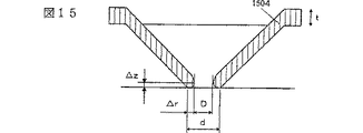
図15は、成膜後のシリコン基板に形成された開口の断面図である。図15において、光反射膜として金属膜1504が膜厚tで成膜されている。ここで、膜厚tとは、シリコン基板1401の上面(テーパ部1402を除く面)に垂直な方向において、シリコン基板1401の上面からの金属膜1504の厚みを示す。金属膜1504が、テーパ部1402上に十分に厚く成膜されることによって、微小開口1403周辺には金属膜1504が微小開口1403の中心に向けて突出量Δrだけ突出し、元の微小開口(以下、修正前の微小開口と称する)の大きさdより小さな、大きさDの微小開口(以下、修正後の微小開口と称する)が形成される。すなわち、生成される近視野光の強度は、修正後の微小開口により規定される。よって、D=d−2Δrの関係が成り立つ。ここで、突出量Δrとは、シリコン基板1401の底面に沿った方向において、修正前の微小開口のエッジ部から、金属膜1504の突出部までの長さを示す。
また、図15に示すように、修正後の微小開口の大きさDは、シリコン基板1401の底面に沿った方向における金属膜1504により規定されるのではなく、シリコン基板1401の底面からΔzだけ上方にずれた位置において規定される。すなわち、このΔzは、修正後の開口と修正前の開口との高さずれを示す。ここで、近視野光の生成条件を満たすにはD<λであればよいが、特にレンズによる回折限界以下の開口サイズを必要とするため、D<λ/2の関係を満たす必要がある。
突出量Δrは膜厚tに比例するので、この膜厚tによって、修正後の微小開口の大きさDを制御することができる。図16(a)は、成膜方向を図14中の矢印Aとした場合の修正後の微小開口の上面図である。図16(a)に示すように、修正前の微小開口1403から内側に突出量Δrだけずれて形成された開口部が、近視野光を生成するために有効な大きさおよび形状となる。
図17は、成膜方向AからAlをテーパ部上に成膜した場合の膜厚tと突出量Δrの関係を示す図である。特に、図17においては、成膜方法として、真空蒸着法とスパッタリング法を行なった場合のそれぞれのグラフを示している。なお、この場合の成膜条件は、真空蒸着法においては、真空度3×10⁻⁶torr、蒸着レート700Å/minとし、蒸着された粒子の大きさ(グレインサイズ)は比較的小さく、テーパ部上に均一に成膜される。また、スパッタリング法においては、真空度3×10−3torr、蒸着レート200Å/minとし、グレインサイズは比較的小さく、テーパ部の底ほど膜厚は薄くなるため真空蒸着法の場合よりも突出量は小さくなる。
図17から、膜厚tと突出量Δrの関係は、Δr>t/10と表すことが可能である。すなわち、上記した成膜条件においては、突出量Δrは膜厚tの10分の1以下になることはなく、仮に突出量Δrが膜厚tの10分の1以下となる関係となる場合は、開口サイズや開口形状を制御するには非常に厚い膜を成膜しなければならなくなり効率的ではない。よって、上記した成膜条件程度によって成膜することが好ましい。また、真空蒸着法においては、蒸着レートを上記した成膜条件よりも遅くしてグレインサイズを大きくすることにより、Δr=t/2程度まで突出量Δrを大きくすることが可能である。
図18は、膜厚tと最大突出部の底面から高さずれΔzの関係を示す図である。特に、図18においては、成膜方法として真空蒸着法を行なった場合のグラフを示しており、成膜条件は上記した通りである。図18からΔz〜t/3と表すことが可能である。すなわち、膜厚tが増大するにつれて、高さずれΔzも増大する。
これら図17および図18から、膜厚tを厚くして突出量Δrを増やした場合、修正後の微小開口の大きさDは小さくなるが、高さずれΔzも増大し、近視野光を生成するのに有効となる開口位置が底面から離れてしまう。これは、近視野光は開口から離れるほど指数関数的に減衰するという性質から、高さずれΔzが増大するにつれて、近視野光強度が小さくなることを意味する。また同時に、近視野光は微小開口から離れるほど広がってしまうため、分解能が低下することを意味する。例えば、微小開口と記録媒体間の距離が微小開口の大きさ程度離れると、分解能は約1/2になる。この距離が分解能の限界とすると、修正後の微小開口の大きさDは、Δz<D=d−2Δrと表すことができる。よって、高さずれΔzの増大は好ましくなく、小さいほどよい。
また、例えば真空蒸着法において成膜方向を傾けることで、修正後の微小開口の形状を制御することができる。図16(b)は、成膜方向を図14中の矢印Bとした場合の修正後の微小開口の上面図である。図16(b)は、特に矢印Bをシリコン基板1401に垂直な方向に対して約20度傾けた方向とした場合を示している。図16(b)に示すように、蒸着方向に対向する面に厚く金属膜が形成され、逆の面には薄く金属膜が形成されている。その突出量の増減量は、図16(a)の場合の突出量Δrに対して約20%であることが確認された。
例として、真空蒸着法による成膜の場合、Alの膜厚t=150ナノメートルとすると、Δz=40〜50ナノメートル、Δr=70〜80ナノメートルであり、修正前の微小開口の大きさ(径)d=250ナノメートルが修正後の微小開口の大きさD=100ナノメートルとなり、Δz<Dの上記式を満たす。スパッタリング法による成膜の場合、高さずれΔzも突出量Δrも真空蒸着法より小さくなるので、Δz<Dを当然満たす。
以上においては、テーパ部52上に成膜した場合について説明したが、シリコン基板1401の裏面上に成膜して、微小開口の大きさおよび形状を制御することもできる。図19は、シリコン基板裏面に成膜した後に形成された開口の断面図である。なお、図中において図15と共通する意味の長さには同一符号を付して、その説明を省略する。
図19において、成膜方法として真空蒸着法を行なう場合、膜厚tと突出量Δrの関係はテーパ部1402上に成膜した場合とほとんど差はないが、スパッタリング法を行なう場合、膜厚tと突出量Δrの関係はテーパ部1402のような障害が存在しないため、膜厚tに対する突出量Δrは大きくなる。
また、膜厚tと高さずれΔzの関係は、図18に示したグラフと同様か、さらに高さずれΔzは小さくなる傾向にある。しかしこの場合、高さずれΔzは、大きいほど近視野光の生成に有効な開口が記録媒体に近づくことになるので、上記したテーパ部1402上に成膜する場合とは異なる。よって、図19において、修正後の微小開口の大きさDは、t−Δz<D=d−2Δrと表すことができ、これにより膜厚tを厚くすることはできない。
また、テーパ部1402上とシリコン基板の裏面上との両方から成膜した場合には、基本的には、近視野光を生成するのに有効な微小開口は最も小さな部分で規定される。その場合、最も小さな開口と平面プローブの底面との距離を小さくすることにより、近視野光の生成を効率よく行なうことができる。
なお、以上に説明した膜厚tは、光の侵入長(金属膜に対する伝搬光の染み込み)以上であればよく、侵入長以下でも反射率が低くなるだけで特に問題はない。突出量Δrや突出形状は、成膜方法や成膜条件により異なる。蒸着の場合、方向性がよいので突出量は小さくなる。しかし、テーパ内部の成膜では開口近傍でも十分成膜できる。一方、スパッタリング法では、回り込みが大きいため突出量が大きいが、テーパ部の成膜では開口近辺には成膜しにくい。
また、上記したシリコン基板はSOI(Silicon on insulator)を用いた薄い場合でも、通常のように500ミクロン程度と厚い場合でも良い。テーパ部の形状や作製方法は、異方性エッチングだけでなく、円弧状になる等方性エッチングでも良く、特に限定しない。また、シリコン基板ではなく、ガラス基板を使用し、等方性エッチングなどでテーパ部を形成することもできる。
以上、本発明の実施の形態5における近視野光ヘッドの製造方法では、シリコン基板に目的とする大きさや形状よりも大きな開口を形成し、この開口のテーパ部上および/またはシリコン基板裏面上に成膜する光反射膜の量を制御することにより、近視野光を生成するための微小開口の大きさおよび形状を規定しているので、エッチング処理等によりシリコン基板に開口を微小に形成する際のばらつきの問題を、比較的制御の容易な成膜処理によって解消することができ、歩留まり良く平面プローブを得ることができる。
(実施の形態6)
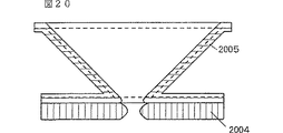
次に、微小開口の大きさや形状を制御する他の近視野光ヘッドの製造方法について説明する。実施の形態5で示したように、シリコン基板に微小開口を形成した後、熱酸化する。このとき、酸化する度合いに応じて、表面に形成される熱酸化膜の膜厚は制御できるが、酸化される部分には体積変化も生じているため、この体積変化量も制御できる。図20は、熱酸化により体積変化が生じて、微小開口の大きさが変化する様子を示す断面図である。図20に示すように、熱酸化膜2005が形成されることにより、元のテーパ部や微小開口の形状(図中の波線)が、実線で示す形状に変化する。
シリコン基板を酸化すると(通常は熱酸化)、酸化膜厚(通常最大で1.2ミクロン程度)に応じて体積変化が生じる。元の形状を点線で示すが、体積変化で実線の形状になる。約1:1で外側と内側に酸化膜の領域が形成される。熱酸化膜厚は通常最大で1.2ミクロン程度なので、最大で内側に600ナノメートル程度(直径では1.2ミクロン程度)開口を小さくできる。イオン注入後などでは、もっと膜厚は厚くなる可能性がある。
酸化膜の膜厚を制御することで、体積変化つまり突出量を制御できる。ただし、酸化膜は通常の光(可視光など)に対しては、透過性であるから、通常は微小な開口形成には金属膜が必要となる。ただしその金属膜は遮光できればよいため、実施の形態5に示したほど厚くなくても良い。金属膜の製膜は上側や下側のどちらでも良く、光の微小開口からの出射効率が変化するだけである。熱酸化だけでなくても、イオン注入などによってもシリコンがアモルファス化して体積変化が生じるので、イオン注入も利用できる。他の体積変化が生じる方法なら、熱酸化やイオン注入に限らない。
以上、本発明の実施の形態6における近視野光ヘッドの製造方法では、シリコン基板に目的とする大きさや形状よりも大きな開口を形成し、この開口のテーパ部を含めた表面を熱酸化またはイオン注入することにより、近視野光を生成するための微小開口の大きさおよび形状を規定しているので、エッチング処理等によりシリコン基板に開口を微小に形成する際のばらつきの問題を、比較的制御の容易な熱酸化またはイオン注入処理によって解消することができ、歩留まり良く平面プローブを得ることができる。
(実施の形態7)
図21は、実施の形態7に係わる近視野光ヘッド2100の一部の断面図を示している。本実施の形態による近視野光ヘッド2100は、逆ピラミッド状の穴をもちその頂点が微小開口を形成する平面基板2101と、微小開口への光の伝搬を行う光導波路2103と、その光導波路2103の一部で構成され、微小開口より突起したピラミッド状の突起部2102と、突起部2102を除く光導波路2103の周囲に形成され、光導波路2103内を伝搬する光を反射する光反射層2104により構成されている。光導波路2103は、光を伝搬するコアとその外周部のクラッドとから構成されていても良い。クラッドの屈折率は、コアの屈折率に比べて相対的に小さい。
図1中には示していないが、レーザ光源あるいは光ファイバより出力された光は、光入射端2105から光導波路2103に入射し、光導波路2103の周りに形成された光反射層2104により反射されながら、光導波路2103の先端部の方向へ伝搬する。光反射層2104の反射効果により、光導波路2103の先端部に多くの光を供給することが可能となる。平面基板2101には、光学的な微小開口が形成されており、光導波路2103の先端部は、この微小開口より突出して、ピラミッド形状をした突起部2102を形成している。この突起部2102の寸法は、高さ200nm以下、底面の一辺の長さ200nm以下であり、光反射層2104は、形成されていない。この突起部2102は、光導波路2103の1部で構成されていることから、多くの光が突起部2102まで伝搬され、その結果、微小開口より突出した突起部2102の周辺に、伝搬光から変換された多くの近視野光を生成することができる。また、平面基板2101より突出したピラミッド形状の光導波路2103の先端部(突起部2102)は、その高さと底面の一辺の比が、√3〜2:2程度の構成であり、光導波路の幅が光の波長より小さくなる領域が、非常に短い構造をしている。この結果、光導波路の幅が光の波長より小さい領域での光強度の減衰が小さくなり、突起部2102より大きな光強度の近視野光を供給することが可能となる。このように多くの近視野光が局在した突起部2を試料表面に近接させることにより、近視野光を試料表面で散乱させ、光の微小領域の光学的な情報を取り出すことができる(イルミネーションモード)。
あるいは、試料表面に局在する近視野光を光導波路2103の先端部である突起部2102で散乱させ、伝搬光として取り出し、光導入端2105の後方で検出器に導入することによっても、微小領域の光学情報を検出できる(コレクションモード)。この場合も、光導波路2103の先端にある突起部2102での光導波路の幅が光の波長以下となる領域が非常に狭い構造をしていることから、近視野光の多くを伝搬光に散乱することが可能となり、また、光反射層2104により、伝搬ロスを少なく光導入端に導くことができる。
また、従来例で述べた平面プローブのように、平面基板内に設けた微小な開口に近視野光を生成させた場合、得られる光像の解像度(分解能)は、その開口サイズと同程度であるが、図21に示す近視野光ヘッド2100では、微小開口より突起した光導波路の一部である突起部2102の周りに近視野光が局在し、その分解能は、この突起部先端の曲率半径に相当するため、微小開口より得られる光像より、高解像度(高分解能)の光像を検出することが可能となる。
また、図21に示した近視野光ヘッド2100において、微小開口より突出した突起部2102の周囲に光反射膜2104は形成されていないが、突起部2102の周りに光反射膜2104を設け、突起部2102の先端に光学的な開口を形成した構成にしても良い。この場合、突起部2102の周りに形成された光反射膜2104の効果により、突起部2102の先端近辺に、より多くの光を供給するとができる。
図22は、図21に示した近視野光ヘッド2100の製造工程を示す説明図である。
はじめに、ステップS501では、基板には、面方位(100)の単結晶シリコンのシリコン基板2200を用いる。面方位(110)、(111)の単結晶シリコンや、ガラス、石英などの誘電体結晶、あるいは、GaAs等の半導体結晶を用いてもよい。
次に、ステップS502では、シリコンの異方性を有するエッチング法にてシリコン基板2200内に逆ピラミッド状の凹部2201を形成する。マスク材となる熱酸化膜を基板上に形成し、所望の個所を、フォトリソグラフィとエッチングによりパターニングし、シリコンを露出させ、水酸化カリウム水溶液、あるいはテトラメチルアンモニウムハイドロオキサイド水溶液といった結晶軸異方性エッチングによりパターニング部のシリコンをエッチングする。このとき、(111)面と等価な4つの面で囲まれた逆ピラミッド状の凹部2201が形成される。また、エッチング溶液に浸すことに代わり、異方性を有するドライエッチング、例えば反応性イオンエッチング(RIE)装置によるエッチングを用いることによっても凹部2201の形成が可能となる。マスク材として、熱酸化膜に代わり、SiO2や窒化膜を用いても良い。その後、マスク材である熱酸化膜を弗化水素酸と弗化アンモニウムの混合水溶液で除去する。
次に、ステップS503では、光反射層2202を成膜する。光反射率の高いAu、Al等の金属膜を真空蒸着法にて凹部2201の底部にまで埋め込むように成膜する。被覆方法として、スパッタリング法やイオンプレーティング法を用いて成膜しても良い。光反射膜2202を設けることにより、光導波路内を伝搬する光を開口に導くことが可能となり、また、外乱光の遮光膜としても機能する。
次に、ステップS504では、光導波路2203となる誘電体を光反射膜2202の上面に成膜する。光導波路2203の材料は、酸化シリコンや窒化シリコン等の誘電体材料、あるいは、ポリイミドやポリメタクリル酸といった高分子材料を使用しても良い。誘電体材料である酸化シリコンの場合、スパッタリング法、CVD法、真空蒸着法によって容易に形成できる。この光導波路2203を屈折率の異なるコア、クラッドにより形成してもよい。この場合、光はコアを全反射して伝搬していくため、伝搬ロスを減少させることができる。
次に、ステップS505では、基板を裏面側よりエッチングし、基板内に光反射膜2202で覆われたビラミッド状の微小な突起部2204を形成する。シリコン基板2200の裏面側をエッチングし、基板の厚みを薄くする。光反射膜2202のビラミッド状の微小な突起部2204が形成されたところでエッチングを終了する。ピラミッドの一辺のサイズは、50nmから3μm程度に形成する。シリコン基板2200のエッチングは、ウェットエッチングを用いても、ドライエッチングを用いても良い。
次に、ステップS506では、基板の裏面側より光反射膜2202である金属膜のエッチングを行い、一辺50〜200nm程度の大きさの微小開口を形成すると同時に、光反射膜を除去した光導波路の一部である突起部2205を形成する。金属膜のエッチングの量をコントロールし、金属膜の開口の大きさを調整する。この結果、光導波路2203の先端に位置する誘電体材料のピラミッド状の微小な突起部2205が形成される。AFM動作時には、この突起部2205の頂点が探針の役割を果たす。金属膜のエッチングは、ドライエッチングを用いても、ウェットエッチングを用いても良い。
次に、ステップS507では、フォトリソグラフィ技術とエッチングを用いて、光導波路2203の形状を作製する。通常の半導体製造工程で用いられるフォトリソグラフィ技術を使用して、光導波路2203上にエッチングを保護するマスク材を積層し、マスク材をパターニングする。その後、光導波路2203をエッチングし、マスク材を除去して、光導波路2203をパターニングできる。光導波路2203の端面の粗さを小さくするために、マスク材および光導波路材料のエッチングは、反応性イオンエッチングや誘導プラズマエッチングに代表される異方性を有するドライエッチング法を用いる。マスク材には、アモルファスシリコン、ポリシリコン、Cr、Al、WSi、Ni、Au等の金属膜、フォトレジストなどを使用する。
次に、ステップS508では、光導波路2203の上面に光反射膜2206を成膜する。光反射率の高いAu、Al等の金属膜を真空蒸着法にて成膜する。被覆方法として、スパッタリング法やイオンプレーティング法を用いて成膜しても良い。光反射膜2206を設けることにより、光導波路2203内を伝搬する光を開口に集光することが可能となり、また、外乱光の遮光膜としても機能する。
以上に示した手順により、図21に示した近視野光ヘッド2100を作製できるが、ステップS507の工程とステップS508の工程を、ステップS505の工程とステップS506の工程の前に行っても、同様に図21に示した近視野光ヘッド2100を作製できる。
以上、本発明の実施の形態7における近視野光ヘッド2100では、光を反射する機能を有した構造をしており、また光導波路の先端に位置する光反射膜2104の開口近辺では、光導波路の幅が光の波長以下となる領域が狭い構造をしており、突起部2102近辺での光損失が小さくなり、光反射層2104で覆われていない突起部2102より光強度の大きい近視野光を容易に発生させることができる。また、突起部2102の先端部の曲率半径と同等の高分解能の光像測定あるいは表面形状観察が行える。
また、半導体製造プロセスに用いられる技術によって微小な開口および近視野光を発生する突起部容易に形成できるため、同一シリコン基板上に複数の近視野光ヘッドを形成するアレイ化が容易となる。また、シリコンプロセスを経て作製するので、バッチ処理が可能となり、量産に適したものとなる。また、ウェハに対する一括した工程で作製できるため、ばらつきが少ない。さらに、製品特性が安定する。また、プローブの小型化が可能となり、ウェハあたりの取り個数が増加するので、コスト低減ができる。
記録媒体として用いられる材料を、例えば相変化記録方式を適用できる材料とした場合に、その記録は光エネルギーのヒートモードを用いるために、光の高密度化は重要な要素となる。従って、近視野光を利用した光記憶の場合も十分に大きな強度の近視野光の生成が望まれ、本発明による光メモリ用ヘッドにおいては、図21中に示した光反射層における開口方面への集光作用によって、あるいは光導波路先端部のピラミッド形状による光導波路幅方向の波長以下領域の縮小によって、その近視野光の強度増強を達成している。また、図21中に示した微小な突起部の先端径に相当するビット間隔のデータの読み出し、書き込みが可能であり、光メモリの記憶ビットの高密度化が実現する。上述した説明においては、光メモリ用ヘッドの突起部に集光して近視野光を生成させる、いわゆる近視野光学顕微鏡で言うイルミネーションモードであるが、他の光学系によって記録媒体面に光を照射し、記録媒体面上の微小な情報記録構造によって生ずる近視野光を微小な突起部によって検出する、いわゆるコレクションモードに対しても本発明による近視野光ヘッドは有効となる。その場合、突起部で検出された近視野光は散乱光に変換されて、光導波路を伝搬し、光入射端に到達する。そこで、光入射端近辺に光検出器を配置する。
また、実施の形態7に係わる光メモリ用ヘッドとして使用する近視野光ヘッドは、一般的な半導体プロセスにて形成されているため、同一シリコン基板上に2次元的に複数個配列させることが容易となる。
図23に、前記光メモリヘッドを同一シリコン基板上に2次元にアレイ状に配置した近視野光ヘッドアレイ2300の構成を示す。1つの光源2302より照射された光が、4つの近視野光ヘッド2301の突起上面に導かれるように光導波路2303が形成される。光源2302によって照射された光は、シリコン基板2304の端面に存在する光導波路2303の入射端に照射され、光導波路2303内に入射される。入射した光は、光導波路2303内を通り、図21と同様に、テーパ部内部に設けた光反射膜により反射されながら、効率良く各々の光メモリヘッド2301の突起部近辺に導かれる。導かれた光によって、各々の突起部からは近視野光が生成される。図23に示した近視野光ヘッドアレイ2300においては、1つの光源に対して、1つのシリコン基板2304上に4つの近視野光ヘッド2301を記しているが、これに限らず、様々な組み合わせが可能である。
上記のように、実施の形態7に係わる光メモリ用ヘッドとして使用する近視野光ヘッドは、同一シリコン基板上に2次元的に複数個配列する構成が可能なため、記憶媒体上おけるヘッドの掃引を最小限に抑え、高速な光記憶及び読み出しが可能となり、更には、前記配列間隔を記録媒体上の情報記録単位間隔に適合させることによってトラッキングレスが実現できる。
(実施の形態8)
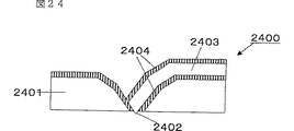
図24は、実施の形態8に係わる近視野光ヘッド2400の一部の断面図を示している。
図24において、実施の形態8に係わる近視野光ヘッド2400は、実施の形態7に係わる近視野光ヘッド2100と同様に、微小開口を有する平面基板2401と、その微小開口より突起し、近視野光の検出および照射を行うピラミッド状の突起部2402と、突起部への光の伝搬を行う光導波路2405と、光導波路の周囲に形成され、光導波路内を伝搬する光を反射する光反射層2404により構成されている。
実施の形態8に係わる近視野光ヘッド2400では、図24に示すように、平面基板2401に形成された穴が、角度の異なる2段の斜面により形成されており、穴の入り口に近い斜面がより広がった形状をしている。そのため、斜面上に形成された光導波路2403は、2箇所で湾曲された形状となる。この場合、光導波路2403の湾曲部1箇所での伝搬光の屈折角は、小さくなり、そこでの光伝搬ロスは低減される。結果、光導波路2403に形成された2カ所の湾曲部において、総じて光の伝搬ロスは低減し、より多くの光を試料に照射することが可能となる。
なお、図24では、角度の異なる2段の斜面により構成された穴をもつ平面基板を示したが、2段に関わらず、3段、4段、あるいは多段な斜面により構成された穴をもつ平面基板を用いても、もちろんよい。
実施の形態8における近視野光ヘッドは、図22に示した実施の形態7における近視野光ヘッドの作製方法と同様な製造プロセスにて作製できる。ステップS501に示した基板内に逆ピラミッド状の凹部をもつ構成のシリコン基板2200を用いて、ステップS512にて、再度、マスク材となる熱酸化膜を基板上に形成し、所望の個所を、フォトリソグラフィとエッチングによりパターニングし、シリコンを露出させ、パターニング部のシリコンをエッチングする。この場合、S111にてエッチングした箇所を含むより広い範囲のシリコンを露出させ、エッチングする。この結果、シリコン基板の(100)面と(111)面との接線より面方位の異なる面が発生し、ステップS512に示した角度の異なる2段の斜面をもつ凹部2207をもつシリコン基板が作製できる。
この後、図22に示した実施の形態7における近視野光ヘッドと同様にステップS503からステップS508の工程を行うことにより、図24に示した実施の形態8における近視野光ヘッド2400を作製する。
以上、本発明の実施の形態8における近視野光ヘッドでは、光導波路の湾曲を多段にし、一カ所の湾曲部での伝搬光の屈折角が小さくなることにより、総じて湾曲部での光の伝搬損出を低減することができ、近視野光を発生する突起部近辺に多くの光を照射することが可能となり、光強度の大きい近視野光を容易に発生させることができる。また、突起部の先端径に等しい高分解能の光像が得られる。
また、実施の形態7と同様に、半導体製造プロセスに用いられる技術によって微小開口および突起部を形成できるため、このような突起部を有するシリコン基板は、近視野光を生成できる平面プローブとして活用でき、コンパクトな構成をしており、特に同一シリコン基板上に複数の突起部を形成するアレイ化が容易となる。また、シリコンプロセスを経て作製するので、バッチ処理が可能となり、量産に適したものとなる。また、ウェハに対する一括した工程で作製できるため、ばらつきが少ない。さらに、製品特性が安定する。また、プローブの小型化が可能となり、ウェハあたりの取り個数が増加するので、コスト低減ができる。
以上、実施の形態7と実施の形態8に係わる近視野光ヘッドは記録再生装置としての近視野光ヘッド以外に、光学顕微鏡用の近視野光ヘッドとしての使用も可能である。また、突起部の先端部を用いて、トンネル電流や原子間力といった相互作用を利用した表面形状の観察や微細構造の加工を行ったり、先端部に磁性膜を着け、試料表面の磁場観察を行うこともできる。
(実施の形態9)
以下、図面を参照して本発明の実施の形態について説明する。図25は、本発明の実施の形態9による近視野光ヘッド2500の構成を示す側断面図である。図25に示す近視野光ヘッド2500において、光導波路2501は、クラッド2502、コア2503およびクラッド2504から構成されており、レーザ光源(図示略)から射出されたレーザ光Laを低損失で伝搬させる。
また、光導波路2501は、石英系材料、高分子等の誘電体材料からなり、クラッド2502、コア2503およびクラッド2504から構成されている。ここで、光導波路2501は、コア2503の屈折率がクラッド2502およびクラッド2504の屈折率より大きくなるように構成されている。上記クラッド2502は、CVD(Chemical Vapor Deposition)、スパッタ、蒸着等の手法により、二酸化珪素膜の堆積によって形成され、その一端部には、表面から裏面に向けて徐々にテーパ状に縮径される逆錐形状のテーパ穴2502aが形成されている。このテーパ穴2502aの頂点は、その径が数十ナノメートルの微小開口2502bとされている。すなわち、クラッド2502の裏面には、微小開口2502bが形成されている。この微小開口2502bの近傍には、近視野光Pが生成される。
コア2503は、クラッド2502の表面およびテーパ穴2502aに沿って、二酸化珪素膜の堆積によって形成され、直線状のコア直線部2503aと、テーパ穴2502aを塞ぐコア先端部2503bとが一体に形成されて構成される。クラッド2504もまた、コア2503の表面における二酸化珪素膜の堆積によって形成される。
また、光導波路2501の一端部2501aは、コア2503のコア直線部2503aに対して所定角度を持つような斜めの一端面T1を有している。この一端面T1には、アルミニウム(Al)、クロム(Cr)、金(Au)等の金属膜や、誘電体多層膜からなる反射膜2505が形成されている。この反射膜2505は、コア2503のコア直線部2503aを同図左方向へ向けて伝搬するレーザ光Laを、その反射面2505aにより微小開口2502b方向へ反射させる役目を果たしている。
基板2506は、シリコン、ガラス等が板状に形成されてなり、クラッド2504(光導波路2501)の表面に接着剤等により接合されている。なお、基板2506とクラッド2504(光導波路2501)とは、陽極接合により接合してもよい。ここで、上記陽極接合とは、基板2506とクラッド2504との間に高電圧を印加することにより境界面において生じるイオン結合による接合をいう。
上記構成において、近視野光ヘッド2500を光メモリの記録再生に適用する場合には、近視野光ヘッド2500の下方に図示しない記録媒体が配設される。上記記録媒体は、例えば円盤状の平面基板であり、相変化記録方式、光磁気記録方式、フォトクロミック記録方式などの光記録/再生を適用できる材料からなり、局所的な光の照射による情報記録を可能とする。また、記録・再生中において、記録媒体は、図示しない駆動機構により高速回転される。
さらに、この場合には、微小開口2502b近傍に生成される近視野光Pを記録媒体に作用させるために、微小開口2502bと記録媒体の記録面との間を微小開口2502bの径程度まで近接させる必要がある。そこで、この例では、近視野光ヘッド2500と記録媒体との間に潤滑剤を充填し、この潤滑剤の表面張力を利用して近視野光ヘッド2500と記録媒体の記録面との距離を十分に小さく維持する。また、上記潤滑剤は、高速回転中に生じる記録媒体の回転軸方向の撓みに近視野光ヘッド2500の位置を追従させる役目をしている。また、微小開口2502bと記録媒体の記録面との間を微小開口2502bの径程度まで近接させる手段として、従来のハードディスクに用いられているフライングヘッド方式を採用することも可能である。
このような状態において、図示しない近視野光ヘッド制御機構によって、近視野光ヘッド2500の微小開口2502bが、記録媒体の記録面における所望の位置に配置されるように、近視野光ヘッド2500の位置が制御される。続いて、図示しないレーザ光源から射出されたレーザ光Laが光導波路2501のコア2503の入射端面に入射されると、該レーザ光Laは、コア直線部2503aを同図左方向に伝搬した後、反射膜2505の反射面2505aにより微小開口2502b方向へ反射される。これにより、微小開口2502bの近傍、言い換えれば、微小開口2502bと記録媒体の記録面との間の微小空間に近視野光Pが生成される。
そして、上記近視野光Pと記録媒体の記録面との相互作用によって生じた伝搬光が、記録面の記録状態に依存した強度や位相等の特性を伴って図示しない受光素子へと導かれて電気信号に変換され、図示しない信号線を介して同じく図示しない信号処理部によって情報記録部の記録状態が判断される。
記録媒体への情報の記録は、上述のように微小開口2502bから近視野光Pを照射する必要があるが、記録媒体に記録された情報の読み出しに関しては、微小開口2502bで近視野光を検出する構成や、同一の微小開口2502bを用いて近視野光の照射と信号光の検出を行う構成も可能である。
次に、図26(a)〜図26(f)を参照して、上述した実施の形態1による近視野光ヘッド2500の製造方法について説明する。まず、図26(a)においては、上述したCVD、スパッタ、蒸着等の手法により、シリコン基板10の表面に二酸化珪素の薄膜が、200nm〜50μmの厚さとなるように、クラッド2502が堆積形成される。次に、フォトリソグラフィの手法を用いて、クラッド2502にテーパ穴2502aが形成される。
具体的には、クラッド2502の表面に塗布されたレジスト部分に、直径が100nm〜1μmのピンホールを形成した後、等方性のドライエッチング手法によりエンチングを施す。これにより、レジスト部分とピンホール近傍のクラッド2502が同時に横方向、縦方向共に同じエッチング速度でエッチングされ、結果的に同図に示すようなテーパ形状のテーパ穴2502aがクラッド2502に形成される。ここで、テーパ穴2502aのテーパ角は、クラッド2502とレジスト剤とのエッチング選択比を調整することにより、変化させることができる。また、異方性のドライエッチングを用い、クラッド2502とレジストとのエッチング選択比を調整することにより、所望の形状のテーパ穴2502aを形成することも可能である。
次に、図26(b)において、クラッド2502の形成手法と同様の手法により、クラッド2502の表面に沿い、かつテーパ穴2502aを塞ぐようにして、二酸化珪素の薄膜が、2μm〜10μmの厚さとなるように堆積形成されることにより、コア2503が形成される。次いで、同様の手法により、コア2503の表面には二酸化珪素の薄膜が200nm〜50μmの厚さとなるように堆積形成されることにより、クラッド2504が形成される。これにより、クラッド2502、コア2503およびクラッド2504からなる光導波路2500がシリコン基板2510の表面に形成される。
ここで、コア2503の屈折率をクラッド2502、2504の屈折率より大きくする手法としては、2つの手法がある。クラッド2502,2504の屈折率を小さくする場合には、クラッド成膜時にフッ素(F)をドーピングすればよく、一方、コア2503の屈折率を大きくする場合には、コア成膜時にゲルマニウム(Ge)をドーピングすればよい。また、成膜方法にもよるが、例えば、CVDやスパッタにより二酸化珪素膜を堆積形成する場合、成膜時のガス圧や印加電力の調整により、上記屈折率を調整することも可能である。
次に、図26(c)において、フォトリソグラフィの手法により、一端面T1を形成するためのレジストパターンを光導波路2501に形成した後、光導波路2501全体をテーパエッチングする。このテーパエッチングの手法としては、次の(1)項〜(3)項に挙げる手法が適宜選択される。
(1)レジストパターンをマスクとし、レジストと光導波路2501の構成材料である二酸化珪素のエッチングレートとを適に選定した状態で異方性または等方性エッチングを施すことにより、レジスト材と二酸化珪素のエッチング速度差に応じた角度で、光導波路2501の一端部2501aが同図に示す形状となるような一端面T1が形成される。
(2)光導波路2501の表面にレジストパターンを形成した後、等方性のドライエッチングを施すことにより、アンダーカットによって一端部2501aが同図に示す形状となるような一端面T1が形成される。
(3)光導波路2501の表面に一端面T1に対応するようなテーパ状のレジストパターンを形成した後、光導波路2501の構成材料である二酸化珪素とレジストのエッチングレートを適に選定した状態で異方性エッチングを施すという、転写方式のエッチングにより、一端部2501aが同図に示す形状となるような一端面T1が形成される。
次に、図26(d)において、光導波路2501(シリコン基板2510)の表面全体には、CVD、スパッタ等の手法により、上述したアルミニウム(Al)、クロム(Cr)等の金属膜、誘電体多層膜等が形成される。次いで、フォトリソグラフィ、エッチングにより、同図に示す反射膜2505以外の膜を除去する。なお、反射膜2505は、後述する図26(e)または図26(f)に示す工程において、同図左方向から堆積形成してもよい。
次に、図26(e)において、光導波路2501(クラッド2504)の表面には、上述した陽極接合または接着剤により基板2506が接合される。そして、最終工程として、図26(f)において、水酸化カリウム(KOH)、テトラメチルアンモニウムハイドロオキサイド(TMAH)を用いて、図26(e)に示すシリコン基板2510にウェットエッチングを施すことにより、シリコン基板2510を除去する。また、シリコン基板2510は、高速度のドライエッチングにより除去することも可能である。これにより、近視野光ヘッド2500が製造される。
以上説明したように、上述した実施の形態9による近視野光ヘッドによれば、従来の光ファイバに代えて、光導波路を用いているので、小型・軽量化を図ることができるため、高速応答が必要とされるフィードバック系の応答速度に容易に追従させることが可能となり、ひいては、高密度の記録再生を行うことができる。
また、上述した実施の形態9による近視野光ヘッドによれば、光導波路を介して、レーザ光源からのレーザ光を微小開口の直近まで導く構成としたので、従来のものと比較して光伝搬損失を飛躍的に減少させることができる。
さらに、上述した実施の形態9による近視野光ヘッドによれば、等方性または異方性のドライエッチングによりテーパ穴を形成しているので、テーパ穴のテーパ角を容易に調整することができ、ひいてはこのテーパ角の調整により光伝送効率を最適値にすることができるので、結果的に光伝搬損失を減少させることができる。
また、上述した実施の形態9による近視野光ヘッドの製造方法によれば、図26(a)〜図26(f)を参照して説明した手法、つまり、シリコン基板の表面に上方向に順次クラッド、コアおよびクラッドを形成した後、基板を光導波路に接合するという手法を用いたことにより、従来、製造が困難とされていた光導波路コアの突起状の形状を容易に形成することができる。
(実施の形態10)
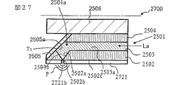
図27は、本発明の実施の形態10による近視野光ヘッド2700の構成を示す側断面図である。図27において、図25の各部に対応する部分には同一の符号を付け、その説明を省略する。図27においては、反射膜2721が新たに形成されている。この反射膜2721は、クラッド2502の裏面2502cに形成されており、この反射膜2721において、微小開口2502bに対応する部分には、微小径穴2721aが形成されている。この反射膜2721は、微小開口2502b周囲の漏れ光を防止し、また、コア2503内を伝搬する光がクラッド2502に漏洩光として漏洩したときに、この漏洩光が光ディスクの記録面に照射されることを防ぐ役目をする一方、近視野光Pの散乱により得られる伝搬光を、図示しない受光素子側へ反射させる役目をしている。
また、反射膜2721は、クラッド2502の裏面2502cに、前述したCVD、スパッタ、蒸着等の手法により、アルミニウム(Al)、クロム(Cr)、金(Au)等の金属膜や、誘電体多層膜が100nm〜1μmの厚さとなるように形成されたものである。さらに、反射膜2721の微小径穴2721aは、上述したリソグラフィ、エッチングの手法により形成される。
この実施の形態10による近視野光ヘッドによれば、反射膜を形成したことにより、コアの漏洩光が光導波路の外部に漏洩することがないため、記録媒体の記録面における光照射範囲を効果的に狭めることができる。さらに、この実施の形態10による近視野光ヘッドによれば、反射膜を形成したことにより、近視野光Pを散乱させて得られる伝搬光が受光素子に効果的に導かれるため、検出感度を向上させることができる。
(実施の形態11)
図28は、本発明の実施の形態11による近視野光ヘッド2800の構成を示す側断面図である。この図において、図25の各部に対応する部分には同一の符号を付ける。この図においては、光導波路2501の一端部2501aの一端面T2が曲面とされており、この一端面T2には、反射膜2505(図25参照)と同様の材料および手法による反射膜2831が形成されている。つまり、反射膜2831の反射面2831aは、一端面T2が曲面であるため、凹面鏡としての役目をしている。すなわち、コア2503のコア直線部2503aを伝搬してきたレーザ光Laは、反射面2831aにより集光されて微小開口2502b方向へ反射されるのである。
この実施の形態11による近視野光ヘッドによれば、反射膜を曲面としたので、レーザ光を集光することができ、ひいては、近視野光の光強度を高めることができる。
(実施の形態12)
図29は、本発明の実施の形態12による近視野光ヘッド2900の構成を示す側断面図である。図29において、図25の各部に対応する部分には同一の符号を付け、その説明を省略する。図29においては、図25に示すクラッド2504が形成されていない構成とされている。すなわち、コア2503の表面には、コア2503の屈折率より小さい屈折率を有する基板2506が、前述した陽極接合等により結合されており、基板2506は、クラッド2504の役目を担っている。従って、図29においては、クラッド2502、コア2503および基板2506により光導波路2901が構成されている。
従って、この実施の形態12による近視野光ヘッドによれば、実施の形態9に記載の近視野光ヘッドと比較して、クラッドが無い分、さらに小型・軽量化を図ることができるため、さらに高密度な記録・再生を行うことができる。
以上本発明の実施の形態9から12について詳述してきたが、具体的な構成はこれらの実施の形態9から12に限られるものではなく本発明の要旨を逸脱しない範囲の設計変更等があっても本発明に含まれる。例えば、上述した実施の形態9から12においては、複数の構成例について説明したが、各構成例を個別的に実施することはもちろんのこと、これらの複数の構成例を適宜組み合わせた構成も本発明に含まれる。
また、実施の形態9から12において、光導波路に導入される光は、レーザ光のように特にコヒーレントな光である必要はなく、インコヒーレントな光であるLED等から射出される光を用いてもよい。
(実施の形態13)
図30は、実施の形態13に係る近視野光ヘッドの構成を示す一部の断面図である。図13に示す近視野光ヘッド3000において、レーザ光源から射出されたレーザ光を近視野光ヘッド3000内に導入させる光導入部において、メディア面に水平な方向に低損失で伝搬させる光導波路3002と、光導波路3002を低損失で伝搬した光を反射させ伝搬方向を開口方向に向ける光反射層3001とを有する第1の基板3003と、開口方向に向かうレーザ光をレンズ効果により集光させ、集光した微小なビームスポットを開口に合わせるように設計されたレンズ3004を有する第2の基板3005と、メディアに対向するスライダ面3006に向け除々にテーパ状に縮径され、上面に光を反射することで開口への光の照射を多くする光反射膜3010が成膜された逆錐形状の穴3007が形成され、その頂点に伝搬光を照射することにより近視野光を生成する微小開口3008が設けている第3の基板3009とから構成されている。
第1の基板3003において、光導波路3002は、石英系材料、高分子等の誘電体材料からなり、図30に示すようクラッド3011、コア3012およびクラッド3013から構成されていても良い。ここで、光導波路3002は、コア3012の屈折率がクラッド3011およびクラッド3013の屈折率より大きくなるように構成されている。上記コア3012およびクラッド3011、3013は、CVD(Chemical Vapor Deposition)、スパッタ、蒸着等の手法により、二酸化珪素膜の堆積によって形成されることにより第1の基板3003の小型化が可能となる。この光導波路3002からの出射光は、所定の角度を持つ斜面上に形成された光反射層3001に照射され、この光反射層3001により光の伝搬方向が変化する。第1の基板3003としてSiliconの(100)基板を用いた場合、異方性エッチングにより形成される(111)により54.7°の斜度をもつ斜面が形成され、その上面にアルミニウム、クロム、金等の金属膜や誘電体多層膜からなる光反射層3001が形成される。この光反射層3001によりメディア面に対し平行な方向から照射された半導体レーザからの光を、スライダの平面内に形成された徴小開口に上方より照射することが可能となり、光伝搬効率の良い近視野光ヘッド3000が可能となる。また別の第1の基板3103として、図31に示すように、光導波路3102のパターンを斜面上さらに上段まで形成した場合でも、メディア面水平方向を伝搬してきた光は、斜面上に形成された光反射層3101により徴小開口方向へ伝搬していく。あるいは別の第1の基板3203として、平坦な基板上に石英系材料を積層し、その石英系材料にマスク形状を転写するような形でエッチングすることにより、一定のテーパ角をもつ斜面を形成し、その上面に金属膜等を積層させ、光反射層3201を形成しても良い(図32)。あるいは、また別の第1の基板3303として、平坦な基板上に蒸着、スパッタあるいはめっき法を用いてアルミや金、あるいは銀、銅、チタン、クロム等の金属膜を積層させ、マスク下のアンダーカットが大きいウェットエッチングあるいはマスク形状の転写が可能なドライエッチングにより、テーパ角をもつ光反射層3301を形成しても良い(図33)。また、図34に示すような光反射層3401近辺に光ファイバ3402をV字型の溝に挿入した基板を第1の基板3403として使用しても良い。この場合、レーザ光源から射出された光は、ファイバ3402内部に形成された屈折率の大きい部分であるコアに入射され、コア内部を伝搬した光は、基板内に挿入された光ファイバの端面3404より光反射層3401に照射される。先ほどのように第1の基板としてSiliconの(100)基板を用いた場合、エッチングレートの遅い(111)面を利用することにより54.7°の斜度をもつ3つの斜面で構成された所望の深さの溝が形成され、円形の光ファイバ3402をその溝内に配置するより高精度なアライメントおよび位置合わせが可能となる。こういった第1の基板(3003、3103、3203、3303、3403)において、光反射層の反射面が凹曲面形状をしていることによる集光機能を有していても良い。また、メディア面と平行な方向に伝搬する光導波路の入射端面あるいは出射端面が凸曲面の形状を有していたり、光導波路の一部にグレーティング機能を有していても良い。これら集光機能により光のスポットが微小開口に合うよう設計され、この効果により微小開口に多くの光を照射でき、情報の高速再生あるいは記録が実現する。
第2の基板3005では、一部に屈折率が異なる屈折率分布をもつ基板を使用する。この基板は、基板の一方の面から他方の面に向かって屈折率が連続的に変化しているため、一方の面に入射した光を他方の面に集光あるいはコリメートすることが可能なレンズ機能を有する。このような基板は、後述する選択イオン交換法により作製する。また、レンズ形状によるレンズ効果をもつ基板を使用しても良い。レンズ形状は、選択イオン交換において半径の大きなイオンを選択することにより、交換されるイオン半径の違いにより円形の膨らみをもつ現象を利用して作製する。また、レンズ形状の別の作製方法として、ドライエッチングのマスクとなるレジストの形状をグレースケールマスクあるいはイマージョンマスクを用いたフォトリソグラフィ技術にてレンズ形状に作製し、基板材料となる誘電体とレジストとの選択比を一定としたエッチング条件にて、基板とレジストを同時にエッチングすることにより所望のレンズ形状を作製できる。このように適切な光学設計されたレンズ機能を有した第2の基板3005を、第1の基板3003と第3の基板3009の中間位置に配置することにより、第3の基板3009に作製される微小開口3008に多くの光を供給することが可能となる。また第2の基板3005として一部にグレーティング機能をもつ基板、あるいはフレネルゾーンプレートやホログラフィックレンズを使用しても良い。このような第2の基板3005の材料としては、誘電体とくに石英やガラスといったSiO2系の材料が用いられる。
第3の基板3009にはシリコン基板を使用する。シリコン基板にはテーパを有する穴3007がこれを貫通するように形成され、メディア側の面内に微小開口3008を有している。穴径はスライダ方向に向かって縮小し、穴の上方より照射された伝搬光は、テーパ内部を反射しながら開口方向に伝搬し、メディア側面内に形成され200ナノメートル以下の微小な径を有する微小開口3008で近視野光に変換される。テーパ部は、異方性を有するシリコンのエッチング技術によりシリコン基板を加工することにより形成される。このテーパ部の上面には、上部より伝搬してきた光を反射し、より多くの光を微小開口に集光できるように光反射膜3010が形成される。貫通した穴を埋めるように上面に積層された光反射膜3010の穴のサイズが微小開口3008の大きさとなる。第3の基板3009において、テーパ部が曲面であったり、あるいは斜度の異なる多段の斜面で構成されていても良い。また穴の内側の一部に屈折率n=1以上の材料が存在し、屈折率分布を持っていたり、曲面形状を持っていても良い。
実施の形態13に係る近視野光ヘッド3000は、上記第1から第3の基板を一体に接合することにより形成される。接合に際し、第1の基板3003に形成した光反射層3001で反射されたレーザ光を第2の基板3005内に存在するレンズ機能により集光し、その収束光を第3に基板3009に設けた微小開口3008に照射することにより大きな近視野光の生成が可能となるようそれぞれの基板の位置合わせを行う。また、所望の大きさの近視野光を得るために、特に第2の基板3005に設けたレンズ3004の大きさやNAの光学設計を行う。基板間の接合は、基板間に接着剤を塗布し、硬化させることにより行ったり、基板材料としてシリコンやガラスを使用していることから、陽極接合方法による基板間の直接な結合を行う。ここで、陽極接合とは、シリコンとガラスもしくはガラスとガラスの間に高電界を生じさせることにより境界面において生じるイオン結合による接合をいう。
次に、図35は、図30に示した実施の形態13における近視野光ヘッド3000の製造工程を示す説明図である。
はじめに、第1の基板3003の作製方法を説明する。まずステップS1101では、基板には、面方位(100)の単結晶シリコン基板3501を使用する。この基板上にマスクとなる熱酸化膜3502あるいは酸化珪素膜をCVD法あるいはスパッタ法により積層させる。マスク材としては、この他に窒化珪素あるいは非アルカリ溶解系金属を用いても良い。次にステップS1102では、リソグラフィの手法を用いてこのマスク材に所望の大きさの窓を開け、エッチングを行う所のSiを露出させる。この後ステップS1103では、水酸化カリウム(KOH)、あるいはテトラメチルアンモミウムハイドロオキサイド(TMAH)を用いて、シリコン基板3501にウェットエッチングを施すことにより段差を設け、(100)に対し54.7°の角度を有する(111)である斜面3503を形成した。続けてステップS1104では、この斜面3503の上面には横方向から伝搬してきた光を開口方向に供給できるようアルミニウム、銀、金等の金属膜や誘電体多層膜からなる光反射層3504を積層形成する。さらにステップS1105で、この後段差の底部に光を伝搬させる材料となる酸化シリコンや窒化シリコン等の石英系材料、ポリイミドやポリメタクリル酸といった高分子等の誘電体材料を堆積させ、光導波路となる材料を作製する。誘電体材料である酸化シリコンの場合、スパッタリング法、CVD法、真空蒸着法によって容易に形成できる。この光導波路を屈折率の異なるコア3506、クラッド3505,3507により形成してもよい。コアの屈折率をクラッドの屈折率より大きくするには、コア成膜時にゲルマニウムをドープすればよく、またクラッドの屈折率をコアの屈折率より小さくするには、クラッド成膜時にフッ素をドープすればよい。このような場合、光はコアを全反射して伝搬していくため、伝搬ロスを減少させることができる。続けてステップS1106でフォトリソグラフィ技術とエッチングを用いて、光導波路3508の形状を調整する。通常の半導体製造工程で用いられるフォトリソグラフィ技術を使用して、光導波路上にエッチングを保護するマスク材を積層してパターニングを行なう。その後、光導波路材料をエッチングし、マスク材を除去することにより、光導波路3508をパターニングできる。このようにして第1の基板3003を作製するが、段差の底部に光導波路を形成せず、光ファイバを挿入してもよい(図34)。この場合、ステップS1101からステップS1104と同様の工程を用いて基板を作製し、(100)と54.7°の角度をもつ2つの(111)で形成されたV字型の溝にこのファイバを挿入する。V溝斜面の角度が一定であるため、エッチングのマスク形状を形成するときに任意のサイズを設定することにより所望の大きさのV溝が形成でき、その結果、V溝上に配置される円形をした光ファイバの位置は決定される。この結果、光反射層に照射する光の位置精度向上が図れる。ファイバの固定は、ファイバを適切な位置に合わせた後、接着剤による接合あるいは陽極接合を用いることにより行う。
また、図32と図33に示した第1の基板では、それぞれ基板上に積層した金属または酸化珪素や窒化珪素といった誘電体材料をテーパ状にエッチングすることにより形成される斜面で光の反射を行う。
次に、第2の基板3005の作製方法を図36で説明する。まず、ステップS1201では、ガラス基板3601上にマスク材となる金属膜3602を積層させる。真空蒸着あるいはスパッタリングにて形成する。
次に、ステップS1202では、フォトリソグラフィ技術を用い、金属膜3602に円形状の穴をあけ、レンズ機能を形成する所のガラス基板3601を露出させる。
次に、ステップS1203では、ガラス基板を溶解塩に浸すことにより、選択イオン交換を行う。ガラス基板内に拡散されるイオンは、マスクの開口部より同心円状に侵入し、3次元的な濃度分布をもつようになる。この結果、この分布に比例した屈折率勾配をもつ基板となる。
最後に、ステップS1204では、マスク材を剥離し、マイクロレンズ基板が形成される。
また、続けてドライエッチングを用いて作製するレンズ形状をもつ基板の作製工程を図37説明する。
まず、ステップS1211では、ガラス基板3701上にレジスト3702を塗布する。
次に、ステップS1212では、階調を有するグレイスケールマスクあるいはイマージョンマスクを用いたリソグラフィによりレンズ形状をしたレジストを露光と現像により作製する。
次に、ステップS1213では、ガラスとレジストとの選択比を一定にしたエッチング条件にてガラス基板をエッチングすることにより、レジストの形状がガラス基板上に転写され、レジストがガラス基板上で完全にエッチングされたところで、このレンズ形状を有する基板は完成する。
続けて、第3の基板3009の作製方法を図38で説明する。まず、ステップS1301では、基板には、面方位(100)単結晶のシリコン基板3801を用いる。面方位(110)、(111)の単結晶シリコンや、ガラス、石英などの誘電体結晶、あるいは、GaAs等の半導体結晶を用いてもよい。
次に、ステップS1302では、単結晶シリコンの面方向によるエッチングレート差による異方性を有するエッチングを利用してシリコン基板内に逆ピラミッド状の貫通した穴3802を形成し、その頂点に開口を設ける。マスク材となる熱酸化膜を基板上に形成し、所望の個所を、フォトリソグラフィとエッチングによりパターニングし、シリコンを露出させ、水酸化カリウム水溶液、あるいはテトラメチルアンモニウムハイドロオキサイド水溶液といった結晶軸異方性エッチングによりパターニング部のシリコンをエッチングする。このとき、(111)面と等価な4つの面で囲まれたテーパを有する逆ピラミッド状の穴3802が基板を貫通して形成される。テーパ角は(111)と(100)により決まる54.7°となり、穴径はスライダ面に近づくにつれ縮小しスライダ面には一辺が1μm以下の微小な開口となる。また、エッチング溶液に浸すことに代わり、異方性を有するドライエッチング、例えば反応性イオンエッチング(RIE)装置によるエッチングを用いることによっても逆錐状の穴の形成が可能となる。マスク材として、熱酸化膜に代わり、酸化珪素膜や窒化珪素膜を用いても良い。その後、マスク材である熱酸化膜を弗化水素酸と弗化アンモニウムの混合水溶液で除去する。
次に、ステップS1303では、逆錘状の穴の上面に光反射膜3803を積層形成する。光反射率の高い金、銀、アルミ等の金属膜を真空蒸着法にて穴の内部に成摸する。被覆方法として、スパッタリング法やイオンプレーティング法を用いて成膜しても良い。光反射膜3803を設けることにより、上方より照射された光が斜面にあたった場合でもその光を反射させることにより開口により多くの光を導くことが可能となる。この結果、開口より多くの近視野光を生成できる。また、外乱光の遮光膜としても機能する。また、この光反射膜の積層により微小開口3804のサイズが決定される。ステップS1302の工程で基板のエッチングにより形成された開口は、穴の内側に光反射膜を積層することでそのサイズは縮小し、光反射膜による開口が近視野光を発生させる微小開口3804となる。
従って、この実施の形態13による近視野光ヘッドによれば、レーザ光源より出射された光を損失少なく開口へ伝搬させ、特にレンズの効果あるいは開口近辺のテーパ状の反射効果によりに多くの光を微小開口に供給できる。また、メディアに平行な方向よりヘッド部に光を入射させる構成によりに高速に動くメディアに近接させながら一定の距離を保つことが可能となる。この結果、高密度な情報の記録再生を高速で実現できる。また、量産可能な微細加工工程にて作製することによりヘッドの小型化および低価格化が実現する。
(実施の形態14)
図39は、実施の形態14に係る近視野光ヘッド3900の構成を示す一部の断面図である。実施の形態14における近視野光ヘッド3900では、第1の基板3901と第2の基板3902について、実施の形態13に示した第1の基板3003と第2の基板3005と同様であるが、近視野光を生成する微小開口3904を有する第3の基板3903は、図39に示す誘電体から成る錘状の突起3905の先端に金属膜3906の開口を設けた構成をしている。シリコン基板3907上に積層した石英系材料の一部分を加工することにより錘状の突起3905を形成するが、このとき、近視野光ヘッドのメディア側面内においてエッチングを施さない石英系材料の厚みと同じ材料でできた突起3905の先端部の高さとを同等にし、かつこの面をメディアに近接させることで、メディアと突起3905の先端に存在する微小開口3904との距離を近づけることが可能となり、微小開口3904で生成された多くの近視野光をメディアに照射することが可能となる。また、アルミ、金、銀といった光反射率の高い材料を突起3905の周りに形成する金属膜3906に採用することにより、上方より照射された光を反射し、より多くの光を微小開口に集光できるようになっている。なお、シリコン基板3907には光を透過する突起3904に光を入射できるよう突起3905の底面に向かって大きな穴が形成されている。また、突起3905の形は、円錐でも多角錐でも良い。あるいは釣鐘形のように突起の斜面が一定の角度を有していなくても良い。
また、実施の形態14における別の第3の基板として、光透過率の高い誘電体材料を使用してもよい。例えば、石英、ガラスといった基板を用いた場合、石英系材料を積層することなく、直接基板を加工し、図39と同様な錐形状をした突起を作製し、同様な作製方法で、金属膜あるいは微小開口を形成する。この基板を使用するときは、開口へ照射する光は基板内を伝搬していくため、シリコン基板3907内に形成した大きな穴を形成する必要はない。
実施の形態14に係る近視野光ヘッド3900も実施の形態13と同様に、第1から第3の基板を一体に接合することにより形成される。メディアに照射する所望の大きさの近視野光を得るために、第3の基板3903の厚み、レンズのNAや大きさあるいは厚みを考慮した光学設計に合うようそれぞれの基板の加工を行い、適切な位置合わせを行った後、接合を実施する。接合方法は、実施の形態13と同様である。
次に、実施の形態14における近視野光ヘッド3900の製造工程を示す説明図である。
第1の基板と第2の基板の製造方法は、実施の形態13に係る近視野光ヘッド製造工程と同様であり、説明を省略する。
図40で第3の基板3903の作製方法を説明する。ステップS1311では、実施の形態13と同様、基板には、面方位(100)単結晶のシリコンの基板3907を用いる。面方位(110)、(111)の単結晶シリコンや、ガラス、石英などの誘電体結晶、あるいは、GaAs等の半導体結晶を用いてもよい。
次に、ステップS1312では、酸化珪素の一種であるTEOS膜3908をCVD法にて積層形成させる。その他の材料として光透過率の高い酸化シリコンや窒化シリコン等の石英系材料、ポリイミドやポリメタクリル酸といった高分子等の誘電体材料を用いても良い。
次に、ステップS1313では、フォトリソグラフィ技術と化学エッチング法を用いてTEOS膜3908の一部を錐形状に加工する。この部分が図39における突起3905となる。フォトリソグラフィを用いてエッチングの特性に適合した形状のエッチングマスクを作製するが、ドライエッチングを用いる場合は、エッチングマスクの形状が転写されながらTEOS膜3908のエッチングが進行するため、エッチングマスク自体にあらかじめ突起3905の形状をもたせておく必要がある。このようなエッチングマスク形状を形成するときには、フォトレジストの露光の際にグレイスケールマスクあるいはイマージョンマスクといった階調を有する光学マスクを用いる。このような光学マスクにより決定される特徴的なエッチングマスクの形状により、任意の形状にTEOS膜3908を加工することが可能となる。また、ドライエッチングでもスパッタ系のエッチング法を用いる場合の作製方法はまた異なる。あらかじめTEOS膜3908を柱型あるいは台形に加工する。その後、スパッタ系エッチングを施すことにより、柱あるいは台形の角だけが削れていき、先端の尖った突起形状が作製される。上記ドライエッチングと異なり、ウェットエッチングを用いる場合は、エッチングマスク形状とマスク下のアンダーエッチングの速度を調整することにより任意の形状のTEOS膜の突起を作製できる。まず、エッチングマスク形状を円形、三角形、四角形にした場合、それぞれ、先鋭化した円錐、三角錐、四角錐の形状が形成される。これは、ウェットエッチングの等方性を利用したものである。マスク形状の円形、三角形、四角形は、フォトマスクを用いたレジストの露光と現像により容易に作製できる。またアンダーエッチングの速度を調節することにより任意のテーパ角度をもつ突起を形成することが可能となる。フォトレジストをマスクとして使用する場合は、TEOS膜表面粗さ、レジストの種類、コート方法あるいはベーキング温度の調整を行いTEOS膜とレジストの密着性を最適化することにより任意のテーパ角を作製する。ウェットエッチャントとして、弗化水素酸と弗化アンモニウムの混合液を使用する。
また、スパッタ原理を用いた局所的なエッチングが可能なFIB(Focused Ion Beam)加工技術を用いて錐形状に加工しても良い。
次に、ステップS1314では、突起3905に光を入射できるよう裏面側からシリコン基板3907をエッチングし、大きな穴を形成する。エッチングマスクとなる熱酸化膜をフォトリソグラフィ技術でパターニングし、シリコンを露出させ、シリコンの結晶軸に対し異方性を有するウェットエッチャント(水酸化カリウム水溶液、あるいはテトラメチルアンモニウムハイドロオキサイド水溶液)を用いて穴を形成する。この場合、(111)面のエッチングレートが遅いため、54.7°の4つの斜面で囲まれた逆錘状の穴となる。この穴はシリコンを貫通しており、その結果シリコン裏面側から照射された光は、突起3905の先端に到達することができる。
次に、ステップS1315では、加工したTEOS膜3908の表面に金属膜3906を積層形成する。光反射率の高い金、銀、アルミ等の金属膜3906を真空蒸着法にて成膜する。デポレートの高い蒸着条件により、グレインサイズの小さい成膜が可能となる。被覆方法として、スパッタリング法やイオンプレーティング法を用いて成膜しても良い。金属膜3906を設けることにより、上方より照射された光が突起3905の斜面にあたった場合でもその光を反射させることにより先端により多くの光を導くことが可能となる。
次に、ステップS1316では、突起3905の先端部の金属膜3906を加工し、微小開口3904を形成する。ステップS1315での金属膜3906の成膜で、方向依存性の高い成膜条件にて基板の斜め方向からデポすることにより、突起斜面の厚みに対し、先端部での厚みが薄くなる傾向がある。このような厚み分布をもった金属膜3906をエッチングすることにより先端部に微小開口を形成することが可能となる。また、別の方法として、先端部に微小開口の大きさに相当する穴をもつマスク材を金属膜上面に形成し、先端部の金属膜だけを選択的にエッチングすることにより微小開口3904を作製することも可能である。この場合エッチングのマスクとして、スピンコートすることにより先端部だけ塗布されないで金属膜が露出された状態のフォトレジストを使用したり、あるいはCVD法により先端部のみ薄く形成された誘電体をエッチングすることにより微小開口に相当する大きさの穴が形成されたものを使用することができる。
また、別の加工方法として、金属膜より硬い材料から成る表面が滑らかな平板を、突起先端部の上方より金属膜に押し当て、一定の負荷荷重を加えることにより、金属膜先端部の形状を平板の型にあうよう平らに変化させ、下層のTEOS膜を露出させることにより微小開口を作製しても良い。この場合、平板で押し当てず、先端の尖った形状のもの、あるいは球状のものを先端部に押し当てて、金属膜をその型にはめ込んだ形状に加工することにより微小開口を作製することも可能である。
最後にステップS1317では、金属膜3904の上面に保護膜3909となる誘電体膜を形成する。保護膜3909は30nm以下の厚みに形成する。誘電体膜の形成により、金属膜の計時的な酸化による反射率の低下あるいは光の漏れ、あるいは媒体との接触に起因する光反射膜の剥離による光漏れを抑制することが可能となる。なお、このステップS1317は省略できる場合もある。
従って、この実施の形態14による近視野光ヘッドによれば、実施の形態13の効果に加え、開口を形成している材料の屈折率が空気より大きいことから開口近辺での光伝搬損失がより小さくなり、開口での光エネルギー密度が向上し、多くの近視野光を生成できる。また、開口近辺の斜面の形状を任意に設定でき、目的に合わせた形状の選択ができる。
(実施の形態15)
図41は、実施の形態15に係る近視野光ヘッド4100の構成を示す一部の断面図である。実施の形態15における近視野光ヘッド4100では、第1の基板4101と第3の基板4103について、実施の形態13と同様であるが、レンズ機能を有する第2の基板として、ボールレンズ4102を使用している。ボールレンズ4102は、第3の基板4103の逆錘状の穴の内側に置かれ、第1の基板4101内に形成された光導波路あるいは光反射層を通して伝播してきた光を、その形状あるいは屈折率に相当するレンズの効果により収束光として第3の基板4103に形成された微小開口に照射する。このボールレンズ4102の位置決め精度は、斜面の角度と球の半径の精度で決まるが、第3の基板4103の穴は、(111)面で形成された54.7°の一定の斜度を持つ逆四角錐形状をしているため、非常に高い精度のアライメントができる。また、ボールレンズ4102の屈折率とその表面の曲率の大きさ(球の半径)の調節により、任意のNAをもつ光を微小開口に照射するできる。ボールレンズ4102の材料としては、石英系材料もしくは高分子材料等の誘電体材料を用いる。
また、上記説明では第3の基板4103として実施の形態13で示した基板を用いたが、同様に実施の形態14に示した第3の基板3903を使用しても良い。また、第1の基板として、図31〜図33に示した基板あるいは図34に示したV溝に光ファイバを差し込んだ基板を使用しても構わない。
実施の形態15における近視野光ヘッド4100は、実施の形態13における近視野光ヘッド3000と同様、第1の基板4101から第3の基板4103を接合して形成するが、この接合方法は、実施の形態13と同様、接着剤による接合あるいは陽極接合といった技術を用いる。
実施の形態15における近視野光ヘッド4100の製造工程は、実施の形態13及び実施の形態14の説明で代用する。ボールレンズの製造方法については、省略する。
従って、この実施の形態15による近視野光ヘッドによれば、実施の形態13および実施の形態14の効果に加え、一定角度の斜面内にボールレンズを挿入することで精密なアライメントを必要とせずに、高い位置精度を得ることができる。この結果、レンズ位置決めの工程が省け、生産効率の向上が望める。また目的に合わせ必要とする近視野光の光量は、レンズのNAに依存するところが大きく、ボールレンズの選択により容易に解決できる。
(実施の形態16)
図42は、実施の形態16に係る近視野光ヘッド4200の構成を示す一部の断面図である。実施の形態16における近視野光ヘッド4200では、第1の基板4201と第3の基板4203について、実施の形態13と同様であるが、レンズ機能を有する第2の基板を代用し、第3の基板4203の微小開口近辺に、紫外線をあてると硬化する液体樹脂を球状の微粒子にして吹き付け、半球形になったまま紫外線を照射し硬化させることにより曲面形状によるレンズ効果を発揮する小型のレンズ4202を作製している。
また、上記説明では第3の基板4203として実施の形態13で示した基板を用いたが、同様に実施の形態14に示した第3の基板3903を使用しても良い。この場合の近視野光ヘッド4300を図43に示す。レンズとなる微粒子の吹き付けは、裏面に形成したシリコン基板の穴4301より行い、その穴の奥に存在するTEOS膜4303の面上に小型のレンズ4302を形成する。あるいは第3の基板としてシリコン基板ではないく石英系の基板を選択したときは、錘状の突起を形成した面の反対側の面上に吹き付け、小型のレンズを形成する。また、第1の基板として、図31〜図33に示した基板あるいは図34に示したV溝に光ファイバを差し込んだ基板を使用しても構わない。
実施の形態16における近視野光ヘッドは、第1の基板と第3の基板を接合して形成するが、この接合方法は、実施の形態13に説明した接合方法と同様、接着剤による接合あるいは陽極接合といった技術を用いる。
実施の形態16における近視野光ヘッドの製造工程は、実施の形態13及び実施の形態14の説明で代用する。
従って、この実施の形態16による近視野光ヘッドによれば、実施の形態13および実施の形態14の効果に加え、微粒子の吹き付けとその硬化により任意のレンズを形成でき、量産に適した工程で作製できる。
(実施の形態17)
図44は、実施の形態17に係る近視野光ヘッド4400の構成を示す一部の断面図である。実施の形態17における近視野光ヘッド4400は、第1の基板4401について、実施の形態13と同様であるが、第2の基板と第3の基板を同一基板とし、媒体面側に実施の形態14における第3の基板に形成した突起4402および微小開口4403を形成し、その反対側の面上に実施の形態14における第2の基板に使用した屈折率分布4404、レンズ形状、あるいはフレネルゾーンプレートやホログラフィックレンズを形成した光透過率の高いガラス基板を使用する。ガラス基板に限らず透過率の高い石英系誘電体基板を用いても良い。
このように、レンズ機能と錘状の突起及び微小開口を一連のフォトリソグラフィ工程を用いて一つの基板内に形成することにより、実施の形態14に記載の近視野光ヘッド作製において必要であった第2の基板と第3の基板の貼り合わせ工程が削減され、その貼り合わせ時の位置ずれにより生じた微小開口からの照射光量低下の問題を回避することが可能となる。
また、ガラス基板のメディア側面内に屈折率分布を形成し、この屈折率分布により集光する光が開口に照射されるようにその屈折率分布内に突起4402および微小開口4403を形成しても良い。この場合、屈折率分布をもつ突起4402が形成される。このように突起内に屈折率分布をもつ近視野光ヘッドは、開口近辺にレンズ機能を設けてあり、かつフォトリソグラフィを用いた微細加工プロセスにて作製できるため、その位置合わせ精度が向上し、安定した特性を示し、量産に適した構成となる。さらにこのガラス基板の第1の基板側面内に図44に示すようなレンズ機能を設け、ガラス基板の両面にレンズ機能を設けた構成にしても良い。このような両面にレンズ機能を有するガラス基板は、1つの基板の両面に同じ工程を施すことにより形成しても良く、また片面にレンズ機能を有する2枚のガラス基板を張り合わせることにより形成しても構わない。このように両面にレンズ機能を設けた構成の近視野光ヘッドは、2カ所での集光機能ににより、集光作用が向上し、微小開口から多くの近視野光が生成できるとともに、1つのレンズで集光させ、微小開口に焦点を合わせるようにした場合に比較して、2つのレンズの組み合わせで焦点を合わせられ、レンズとレンズの位置合わせが厳しい精度を必要としないことから比較的容易に作製できる。
(実施の形態18)
図45は、実施の形態18に係る近視野光ヘッド4500の構成を示す一部の断面図である。実施の形態18における近視野光ヘッド4500は、図45に示すように第1の基板、第2の基板、第3の基板に含まれた光学要素(光導波路4501、光反射層4502、突起4503、微小開口4504)をすべて同一基板のメディア側の面内に形成した。
図46は、図45に示した実施の形態18における近視野光ヘッド4500の製造工程を示す説明図である。
はじめにステップS1401では、実施の形態13の第1の基板と同様に、シリコン基板4601に段差を設け、その斜面に光反射層4602を、下段に光反射層4602に光を照射する光導波路4603を形成する。実施の形態18の近視野光ヘッドにおいても、図31から図33に示した第1の基板を使用しても良い。
次に、ステップS1402では、光反射層4602および光導波路4603の上面にTEOS膜4604をCVD法にて積層形成する。他の誘電体材料を用いても問題ない。
次に、ステップS1403では、段差のあるTEOS膜の表面を研磨加工し、平坦化する。
次に、ステップS1404では、実施の形態14における近視野光ヘッドの作製工程ステップS1313と同様の工程を行い、TEOS膜4604に錐状をした突起4605を形成する。
最後に、ステップS1405では、実施の形態14における近視野光ヘッドの作製工程ステップS1315、S1316と同様の工程を実施し、図45に示す、微小開口4504を含む突起4503、光反射層4502、光導波路4501をスライダ面側に形成した実施の形態18における近視野光ヘッド4500を形成する。
このような構成の近視野光ヘッドは光導波路4501の出射端と微小開口4504との光路距離を短くできる。例えば積層する酸化珪素膜の厚みを10μm程度にすることにより、その距離を10μm以下に設定できる。この結果、出射端が離れるほど大きくなる伝搬光のビームスポット径を小さいまま微小開口に照射でき、多くの近視野光の生成が可能となる。またこの近視野光ヘッドの作製は、同一面への成膜とフォトリソグラフィを用いた薄膜の加工により形成され、接合の工程を含まない。よって、実施の形態13から17において問題であった、貼り合わせによって生じる位置ずれを減少させ、微小開口で生成する近視野光の光量向上が望める。
産業上の利用可能性
以上説明したように、本発明の近視野光ヘッドによれば、近視野光ヘッドのフレクチャ機能を障害することなく、メディアに近接してその間隔を常に一定に保つことが可能となる。微小開口とメディアとの距離を近接させながら、メディアに対向した面が滑らかな平面であるために記録媒体との接触による損傷を低減できる構造であるため、壊れにくく丈夫で、しかも信頼性の高く、また、信号SN比の大きな近視野光ヘッドが作製できる。
さらに、ヘッド内には、メディア平行方向に光を伝搬させる光導波路およびその光を開口方向に反射させる機能および発散する光を収束するレンズ機能さらに開口近辺に光を集光するテーパ形状等の光の伝搬ロスを抑える構造に形成してあるため、集光したエネルギー密度の高い光を開口に低損失で伝搬できる。これにより開口より常に多くの安定した近視野光を発生でき、光を用いてSN比が高く信頼性に優れた高密度記録再生方法を可能にした。
さらに、光伝搬体の幅が波長以下となる領域において光強度の減衰が激しくなるが、この領域が狭い構造を得ることにより、微小開口より多くの近視野光を生成することが可能となり、この結果、記録媒体の情報の記録および再生においてSN比の高い信号を扱うことから信頼性の高い近視野光ヘッドを供給できる。
さらに、レーザ光源での光量が少ない場合でも、近視野光への変換効率が高いことから、記録媒体に必要とされる近視野光の供給が可能となる。よって、レーザ光源での電力が節約でき、低消費電力および低電圧駆動可能な情報再生記録装置の供給が可能となる。
さらに、上方より近視野光ヘッドに光を入射させる場合に装置構成が大型化する問題に対し、記録媒体に対し平行方向から近視野光ヘッドに光を導入させることにより、装置全体の小型化、薄型化が可能となるとともに、高速運動する記録媒体のうねりに追従し、常に記録媒体に対して一定の相対位置を保つことが可能であるため、記録媒体に対し常に安定した近視野光の供給が可能となり、信頼性の高い近視野光ヘッドが供給できる。
また、開口から突出した突起部を設けた構成により、突起部先端の曲率半径に相当する高い分解能による微小ビットへの情報記録再生が可能となる。また、突起の形状による特徴的な近視野光の空間分布が生じ、これを利用して効果的に照射範囲を決定できる。
また、本構成の光ヘッドは、シリコンなどを用いた微細加工プロセスにて作製でき、またヘッドへの光をメディアと平行な方向より入射することにより、装置全体の小型化および薄型化が可能となり、同時にバッチ処理可能な量産工程への適用による低コスト化や製品の安定性および高信頼性も実現した。また、2次元に配列したアレイ化に適した構造であり、光メモリヘッドとして使用した場合、高速な光の記憶または再生が可能となる。
また、本発明の近視野光ヘッドの製造方法によれば、目的とする大きさ以上の開口を形成したシリコン基板に対して、金属膜の成膜、熱酸化、イオン注入によって、近視野光を生成するための微小開口の大きさおよび形状を規定するので、エッチング処理等により微小開口の大きさおよび形状を規定するのに比較して、より正確で歩留まり良く近視野光ヘッドを製造することができる。
【図面の簡単な説明】
図1は、本発明の実施の形態1に係る光記憶再生装置の概略図である。
図2は、本発明の実施の形態1に係る近視野光ヘッドのメディア側面の概略図である。
図3は、本発明の実施の形態1に係る近視野光ヘッドのメディア側面の概略図である。
図4は、本発明の実施の形態1に係る近視野光ヘッドのメディア側面の概略図である。
図5は、本発明の実施の形態1に係る近視野光ヘッドの一部を示す断面図である。
図6は、図5に示した近視野光ヘッドの製造工程を示す説明図である。
図7は、本発明の実施の形態1に係る近視野光ヘッドのアレイ化を示す説明図である。
図8は、本発明の実施の形態2に係る近視野光ヘッドの一部を示す断面図である。
図9は、本発明の実施の形態3に係る近視野光ヘッドを構成しているシリコン基板の一部を示す断面図である。
図10は、図9に示した近視野光ヘッドを構成しているシリコン基板の製造工程を示す説明図である。
図11は、本発明の実施の形態4に係る近視野光ヘッドを構成しているシリコン基板の一部を示す断面図である。
図12は、図11に示した近視野光ヘッドを構成しているシリコン基板の製造工程の一例を示す説明図である。
図13は、図11に示した近視野光ヘッドを構成しているシリコン基板の製造工程の一例を示す説明図である。
図14は、本発明の実施の形態5に係る近視野光ヘッドの製造方法においてシリコン基板に形成された開口の断面図である。
図15は、本発明の実施の形態5においてテーパ部上に成膜後の開口の断面図である。
図16は、実施の形態5において修正後の微小開口の上面図である。
図17は、実施の形態5においてテーパ部上に成膜した場合の膜厚tと突出量Δrの関係を示す図である。
図18は、実施の形態5において膜厚tと最大突出部の底面から高さずれΔzの関係を示す図である。
図19は、本発明の実施の形態5に係る、平面基板に形成した微小開口の大きさや形状を制御する様子を示す説明図である。
図20は、本発明の実施の形態6に係る、平面基板に形成した微小開口の大きさや形状を制御する様子を示す説明図である。
図21は、本発明の実施の形態7に係る近視野光ヘッドの一部を示す断面図である。
図22は、図21に示した近視野光ヘッドの製造工程を示す説明図である。
図23は、本発明の実施の形態7に係る光導波路をもつ近視野光ヘッドのアレイを示す説明図である。
図24は、本発明の実施の形態8に係る近視野光ヘッドの一部を示す断面図である。
図25は、本発明の実施の形態9による近視野光ヘッドの構成を示す側断面図である。
図26は、本発明の実施の形態9による近視野光ヘッドの製造方法を説明する側断面図である。
図27は、本発明の実施の形態10による近視野光ヘッドの構成を示す側断面図である。
図28は、本発明の実施の形態11による近視野光ヘッドの構成を示す側断面図である。
図29は、本発明の実施の形態12による近視野光ヘッドの構成を示す側断面図である。
図30は、本発明の実施の形態13による近視野光ヘッドの構成を示す側断面図である。
図31は、本発明の実施の形態13による近視野光ヘッドの一部を示す側断面図である。
図32は、本発明の実施の形態13による近視野光ヘッドの一部を示す側断面図である。
図33は、本発明の実施の形態13による近視野光ヘッドの一部を示す側断面図である。
図34は、本発明の実施の形態13による近視野光ヘッドの一部を示す側断面図である。
図35は、本発明の実施の形態13による近視野光ヘッドの一部の製造方法を説明する側断面図である。
図36は、本発明の実施の形態13による近視野光ヘッドの一部の製造方法を説明する側断面図である。
図37は、本発明の実施の形態13による近視野光ヘッドの一部の製造方法を説明する側断面図である。
図38は、本発明の実施の形態13による近視野光ヘッドの一部の製造方法を説明する側断面図である。
図39は、本発明の実施の形態14による近視野光ヘッドの構成を示す側断面図である。
図40は、本発明の実施の形態14による近視野光ヘッドの一部の製造方法を説明する側断面図である。
図41は、本発明の実施の形態15による近視野光ヘッドの構成を示す側断面図である。
図42は、本発明の実施の形態16による近視野光ヘッドの構成を示す側断面図である。
図43は、本発明の実施の形態16による近視野光ヘッドの構成を示す側断面図である。
図44は、本発明の実施の形態17による近視野光ヘッドの構成を示す側断面図である。
図45は、本発明の実施の形態18による近視野光ヘッドの構成を示す側断面図である。
図46は、図45に示した実施の形態18における近視野光ヘッドの製造工程を示す説明図である。Technical field
The present invention utilizes near-field light generated by optical interaction in a minute area, reproduces structural or optical information formed in the minute area, and records information in the minute area, The present invention relates to a near-field optical head for an information recording / reproducing apparatus capable of reproducing and recording high-density information.
Background art
Information recording / reproducing apparatuses using light have evolved in the direction of larger capacity and smaller size, and therefore higher recording bit density is required. As countermeasures, research using blue-violet semiconductor lasers and SIL (Solid Immersion Lens) has been carried out. However, these technologies can only improve the current recording density by several times due to the problem of light diffraction limit. Absent. On the other hand, an information recording / reproducing method using near-field light is expected as a technique for handling optical information in a minute region exceeding the diffraction limit of light.
In this technique, near-field light generated by the interaction between a minute region and an optical aperture having a size equal to or smaller than the wavelength of light formed in the near-field optical head is used. As a result, it is possible to handle optical information in a region that is equal to or less than the wavelength of light, which is a limit in conventional optical systems. As a method of reproducing optical information, a lot of near-field light localized on a minute mark is converted into propagating light by interacting with a minute aperture by irradiating scattered light on the media surface (collection mode) method, or minute By irradiating the media surface with near-field light generated from the aperture, and detecting the scattered light converted by the interaction with the minute irregularities on which the information on the media surface is recorded (illumination mode) Is possible. Recording is performed by irradiating the surface of the medium with near-field light generated from a minute aperture, changing the shape of a minute area on the medium (heat mode recording), or changing the refractive index or transmittance of the minute area ( (Photon mode recording). By using such a near-field optical head having an optical minute aperture exceeding the light diffraction limit, the recording bit density higher than that of the conventional optical information recording / reproducing apparatus can be achieved.
Under these circumstances, the configuration of the recording / reproducing apparatus using near-field light is generally the same as that of the magnetic disk device, and a near-field light head is used instead of the magnetic head. A near-field optical head having an optical micro-aperture attached to the tip of the suspension arm is levitated to a certain height by a flying head technique, and an arbitrary data mark existing on the disk is accessed. In order to make the near-field optical head follow the high rotation of the disk, it has a flexure function that stabilizes the posture in response to the undulation of the disk.
In the near-field optical head having such a configuration, as a method of supplying light to the aperture, means for directly connecting the optical fiber to the head from above or directly irradiating the head with a laser provided above the head has been taken. .
Also, instead of a near-field optical head, an optical fiber probe such as a near-field optical microscope and an optical fiber probe with a sharpened opening or a cantilever-type optical probe are used. Information was recorded and reproduced while maintaining the relative position to the media by the interaction of the tunnel current and atomic force generated between the two.
In addition, the use of a planar probe in which an opening of an inverted pyramid structure is formed on a silicon substrate by anisotropic etching has been proposed. Light is incident from above, and near-field light is generated from an opening at the apex thereof by reflection in an inverted conical pyramid. Since this probe does not have the above-mentioned sharpened tip, it can be used as an optical head suitable for high-speed recording and reproduction.
However, when light is incident with a structure in which an optical fiber is connected from above, the optical fiber structure is connected between the head and the arm, which hinders the free movement of the head and causes the head to react to the disk movement. Due to the difficulty in posture control and the increase in the size of the head, the distance between the disk and the opening could not be kept constant. As a result, the output signal-to-noise ratio from the optical information drawn on the disk is reduced, making it difficult to read and write signals. Also, a lot of light attenuates before reaching the aperture, and it is difficult to generate near-field light sufficient for high-speed reproduction from the aperture. Further, since the fiber protrudes above the head, the apparatus itself becomes large, and it is difficult to reduce the size and thickness. In addition, the optical fiber heads were inserted and aligned one by one, and the mass productivity was poor.
In addition, when a signal is directly emitted to the head by a laser disposed above the head, it is necessary to synchronize the incident light in response to the high-speed movement of the head, and a structure that moves in accordance with the movement of the head. It was necessary to provide it separately, which was very difficult. Further, by separately providing such a structure, the apparatus itself becomes large, and it is difficult to reduce the size of the reproducing / recording apparatus.
In addition, when using a fiber optic probe with a sharpened optical fiber or a sharpened cantilever type optical probe to maintain a constant distance from the media by interaction with the media surface, the distance to the media is always controlled. However, since scanning is required, a device for the feedback mechanism is required, and it is difficult to reduce the size of the recording / reproducing apparatus. In addition, there is a problem with high-speed sweeping due to the limited response speed of the feedback system. Further, the mechanical strength of the sharpened probe is not sufficient, and it is not suitable for arraying. Also, the near-field light intensity from the aperture is not sufficiently large due to light loss at the fiber tip. Moreover, this probe is produced by hand one by one and is not mass-productive.
Also, in the flat probe, it is necessary to make light incident from above, and similarly to the above-described problems, problems such as an increase in size of the apparatus, a problem with mass productivity, and a decrease in the flexure function occur.
Further, the above-described aperture of the probe needs to be formed to have a size smaller than the wavelength of propagating light (laser light or the like) in order to generate near-field light or to scatter near-field light. It has been difficult to accurately create an opening having a large size (10 nanometers to 200 nanometers) in a target shape and size with high reproducibility.
For example, in the above-described planar probe, an etching process is usually performed to produce a minute opening suitable for generation or scattering of near-field light on a silicon substrate. However, the quality of the silicon substrate and the uneven concentration of the etching solution are problematic. It may become.
Regarding the quality of the former silicon substrate, there is a method of opening a hole penetrating the silicon substrate by forming a tapered portion by anisotropic etching, or isotropic etching (back surface from the back surface of the silicon substrate on which the tapered portion is formed). The method of making the openings appear by etching) is based on the premise that there is a periodic crystal plane of silicon, and the portion containing crystal defects and impurities is not etched in the intended direction and speed, and the final etching is performed. In other words, the shape and size of the opening that can be obtained are distorted.
Further, the latter problem of uneven concentration of the etching solution is that there is some unevenness in the concentration of the etching solution, and due to this unevenness, on the silicon substrate, the portion where the etching proceeds fast and the portion where the etching proceeds slowly, that is, Regions with different etching speeds appear, and the shape and size of the finally obtained opening are distorted. Such a problem cannot be ignored especially when trying to form a large number of planar probes on a silicon wafer, which causes a decrease in yield.
Therefore, the present invention is capable of generating near-field light sufficiently larger than the aperture in a near-field optical head having a minute aperture that generates near-field light, providing high-resolution reproduction recording, and capable of mass production with a compact configuration. Near-field light that is excellent in two-dimensional arraying, can perform stable recording / playback by movement following the media without obstructing the function of the flexure, and enables high-speed recording / playback and downsizing and thinning of the device. The object is to provide a head.
Disclosure of the invention
In order to achieve the above object, in the near-field optical head according to the present invention, a planar substrate formed by penetrating an inverted conical hole so that its apex has a minute opening, and the planar substrate, An optical waveguide formed on a surface opposite to the surface on which the minute opening is formed, and a light reflecting film formed in the optical waveguide and bending the optical path.
Therefore, the light can be condensed in the vicinity of the minute aperture by one-time reflection of the light by the light reflecting layer, the intensity of near-field light generated from the aperture can be increased, and the mechanical strength is large and compact. It is possible to provide a near-field optical head having a simple structure and excellent in mass productivity.
In the near-field optical head according to the present invention, the optical waveguide is also formed inside the inverted conical hole.
Accordingly, the optical waveguide can be arranged near the minute aperture, the light energy density irradiated to the minute aperture is large, the intensity of near-field light generated from the aperture can be increased, and the mechanical strength is large. It is possible to provide a near-field optical head having a compact configuration and excellent mass productivity.
Further, in the near-field optical head according to the present invention, the inverted conical hole is formed by a plurality of inclined surfaces having different inclinations. Further, in the plurality of inclined surfaces, the plurality of inclined surfaces A slope having an inclination smaller than an average inclination is in the vicinity of the minute aperture.
Therefore, the structure having a gentle slope near the minute aperture can reduce the light propagation loss near the aperture, increase the intensity of near-field light generated from the aperture, and increase the mechanical strength. It is possible to provide a near-field optical head having a high strength, a compact configuration, and excellent mass productivity.
Further, in the plurality of slopes, at least one of the slopes is less than 55 degrees with respect to the surface of the flat substrate on which the micro-apertures are formed. Loss can be reduced, and the intensity of near-field light generated from the aperture can be increased.
In the near-field optical head according to the present invention, the inverted conical hole has at least one curved slope. Alternatively, at least one of the curved slopes is characterized in that the inclination decreases near the opening in the vicinity of the minute opening.
Therefore, the structure having a gentle slope near the minute aperture can reduce the light propagation loss near the aperture, increase the intensity of near-field light generated from the aperture, and increase the mechanical strength. It is possible to provide a near-field optical head having a high strength, a compact configuration, and excellent mass productivity.
In the near-field optical head according to the present invention, the light reflecting layer or the optical waveguide may have a function of condensing on the minute aperture or light from the minute aperture (scattered when detecting near-field light). (Light) collimating function.
Therefore, the light can be condensed on the microscopic aperture by the effect of the condensing function configured in the light reflecting layer or the optical waveguide, and the intensity of near-field light generated from the aperture can be increased and the mechanical strength can be increased. It is possible to provide a near-field optical head having a large, compact configuration and excellent mass productivity.
Further, it is possible to provide a near-field optical head capable of efficiently propagating light detected from the minute aperture due to the effect of the collimating function of the light configured in the light reflecting layer or the optical waveguide.
The near-field optical head according to the present invention is characterized in that the optical waveguide is configured by a combination of a clad and a core.
Therefore, a near-field optical head with high light propagation efficiency can be provided by configuring the optical waveguide with a core and a clad having different refractive indexes.
In the near-field optical head according to the present invention, the planar substrate has a plurality of the micro openings, and the optical waveguide and the light reflecting layer are on a surface opposite to the surface on which the micro openings are formed. And is formed so as to guide light emitted from one light source in the direction of the plurality of minute openings.
Therefore, when the near-field optical head according to the present invention is used as an optical memory head, it is possible to record and reproduce information at high speed without performing high-speed sweep of the probe, and to supply a sufficient amount of light to the medium. It is possible to provide an optical probe with a compact structure and excellent mass productivity. Furthermore, more near-field light can be generated than the aperture, signals with a high S / N ratio can be input / output, and a highly reliable device can be manufactured.
Next, in the method for manufacturing a near-field optical head according to the present invention, a planar substrate in which an inverted conical hole is formed so as to penetrate the apex of the hole into a minute opening, and the minute opening of the planar substrate includes: In manufacturing a near-field optical head including an optical waveguide formed on a surface opposite to the formed surface, and a light reflection layer formed on the optical waveguide and bending the optical path, the optical waveguide is It is characterized by being laminated on the flat substrate. Further, the optical waveguide is formed by being bonded on the planar substrate.
In the method for manufacturing a near-field optical head according to the present invention, the step of forming an inverted conical hole penetrating the planar substrate so as to have a minute opening, and the optical waveguide are formed with the minute opening. And a step of forming a light reflection layer on the optical waveguide so as to bend the optical path.
Alternatively, instead of the step of laminating the optical waveguide on the surface opposite to the surface on which the micro openings are formed, the optical waveguide is joined on the surface on the opposite side to the surface on which the micro openings are formed. It is characterized by being performed in the forming step.
Therefore, in such a manufacturing method, it is possible to provide a near-field optical head that can be manufactured by a semiconductor manufacturing process using a photolithography technique, has a compact configuration, good reproducibility, and excellent mass productivity. Further, an arrayed near-field optical head and a near-field optical head array in which a plurality of openings are formed on the same substrate can be provided.
In the method of manufacturing a near-field optical head according to the present invention, a step of forming an inverted conical hole penetrating the apex as a first minute opening on a flat substrate, and a taper portion of the inverted conical hole are formed. Forming a light reflecting layer, and forming a second minute opening having a size defined by the thickness of the light reflecting layer and smaller than the first minute opening.
Therefore, by forming a relatively large minute opening (first minute opening) in a planar substrate such as a silicon substrate, variation of the minute opening due to etching processing or the like is reduced, and the reverse is also true for the scattered minute openings. By performing the film forming process that is relatively easy to control on the tapered portion of the conical hole, the size of the actually effective micro-aperture (second micro-aperture) is defined. Obtainable.
In the method of manufacturing a near-field optical head according to the present invention, a step of forming an inverted conical hole penetrating the apex as a first minute opening on a flat substrate, and a taper portion of the inverted conical hole are formed. Forming a light reflection layer having a partially different thickness on the first reflection layer, forming a second minute opening having a shape defined by the thickness of the light reflection layer and different from the shape of the first minute opening; It is characterized by including.
Therefore, by forming a relatively large minute opening (first minute opening) in a planar substrate such as a silicon substrate, variation of the minute opening due to etching processing or the like is reduced, and the reverse is also true for the scattered minute openings. By performing the film forming process partially different in thickness on the tapered portion of the conical hole, the shape of the actually effective minute opening (second minute opening) is defined, so that a planar probe is obtained with a high yield. be able to.
In the method of manufacturing a near-field optical head according to the present invention, a step of forming an inverted conical hole having a vertex penetrating as a first minute opening in the planar substrate, and the first minute opening in the planar substrate are provided. Forming a light reflecting film on a surface including the second minute opening having a size defined by the thickness of the light reflecting film and smaller than the first minute opening. It is a feature.
Therefore, by forming a relatively large minute opening (first minute opening) in a flat substrate such as a silicon substrate, variation of the minute opening due to etching processing or the like is reduced, and even with respect to a minute opening that is dispersed, The size of the actually effective micro-aperture (second micro-aperture) is defined by performing film formation processing that is relatively easy to control on the back surface of the substrate (on the surface including the first micro-aperture). Therefore, a planar probe can be obtained with a high yield.
In the method of manufacturing a near-field optical head according to the present invention, a step of forming an inverted conical hole penetrating the top of the flat substrate as a first minute opening, and a tapered portion of the inverted conical hole are provided. Forming an oxide film on the surface of the planar substrate, and forming a second minute opening having a size defined by the thickness of the oxide film and smaller than the first minute opening. It is characterized by.
A step of forming an inverted conical hole penetrating the planar substrate so as to have a first minute opening; and ion implantation on a surface of the planar substrate including a tapered portion of the inverted conical hole. And forming a second minute opening having a size defined by the thickness expanded by the ion implantation and smaller than the first minute opening.
Therefore, by forming a minute opening (first minute opening) larger than the target size and shape on a flat substrate such as a silicon substrate and thermally oxidizing or ion-implanting the surface including the tapered portion of the minute opening. Since the expanded portion defines the size and shape of the minute opening (second minute opening) for actually generating near-field light, when the opening is minutely formed in the silicon substrate by etching or the like. Can be solved by thermal oxidation or ion implantation that is relatively easy to control, and a flat probe can be obtained with high yield.
In order to achieve the above object, in the near-field optical head according to the present invention, a flat substrate in which an inverted conical hole is formed so as to have a fine opening at the apex thereof, and the flat substrate An optical waveguide laminated on the surface opposite to the surface where the micro openings are formed, and inside the inverted conical hole, and a portion of the optical waveguide. And a small protruding portion that protrudes from the opening and is sharpened.
Further, a light reflecting layer for reflecting light is formed around the optical waveguide except for the protrusions.
Accordingly, a large amount of light can be supplied to the protrusion that generates near-field light due to the structure of the optical waveguide, and a large amount of light can be supplied in the direction of the tip (protrusion) of the optical waveguide by reflection of light by the light reflection layer. The near-field optical head that can increase the intensity of near-field light generated from the minute protrusions formed at the tip, and has a compact structure with high mechanical strength and excellent mass productivity. it can.
In the near-field optical head according to the present invention, the minute protrusion has a quadrangular pyramid shape.
Therefore, in the protrusion, the area of the optical waveguide whose width is smaller than the wavelength of the light is narrowed, the intensity of near-field light generated from the protrusion can be increased, and the curvature of the tip of the sharpened protrusion can be increased. High resolution corresponding to the radius can be observed.
The near-field optical head according to the present invention is characterized in that the inverted conical hole is formed by a plurality of inclined surfaces having different inclinations.
Therefore, by adopting a structure in which the optical waveguide has a gently curved shape, the loss of light propagation in the curved portion can be reduced as a whole, and the intensity of near-field light generated from the protrusion can be increased.
The near-field optical head according to the present invention is characterized in that the optical waveguide is constituted by a combination of a clad and a core.
Therefore, a near-field optical head with high light propagation efficiency can be provided by configuring the optical waveguide with a core and a clad having different refractive indexes.
In the near-field optical head according to the present invention, the planar substrate has a plurality of the minute projections, and the optical waveguide and the light reflection layer emit light emitted from at least one light source. It is characterized by being formed so as to be guided in the direction of the minute protrusions.
Therefore, the structure having the optical waveguide and the light reflection layer allows light to be efficiently propagated to a minute projection located at the tip of the optical waveguide, and the width of the optical waveguide at the projection is the wavelength of the light. By narrowing the area of smaller dimensions, the intensity of near-field light generated from the protrusion can be increased, and high-resolution observation corresponding to the radius of curvature of the tip of the sharpened protrusion can be achieved. A possible near-field optical head can be provided. In addition, a near-field optical head having a high mechanical strength, a compact configuration, and excellent mass productivity can be provided. By scanning such a probe two-dimensionally, it is possible to process a high-resolution near-field optical image as a whole at high speed. In addition, an optical probe capable of recording and reproducing information at a high speed without requiring a high-speed sweep of the probe can be provided.
Next, in the method for manufacturing a near-field optical head according to the present invention, a step of forming an inverted conical hole in the planar substrate, and an optical waveguide on the planar substrate including the inside of the inverted conical hole. A step of forming a layer, a step of forming a minute protrusion for detecting or irradiating light on a surface of the flat substrate opposite to the inverted conical hole, and a light reflecting layer so as to bend the optical path. And a step of forming the optical waveguide.
Also, a planar substrate formed with an inverted conical hole penetrating so that its apex has a minute opening, a surface of the planar substrate opposite to the surface on which the minute opening is formed, and the reverse An optical waveguide laminated inside a conical hole, and a small protruding portion formed by a part of the optical waveguide and protruding from a minute opening of the flat substrate and sharpened. In manufacturing the near-field optical head, the optical waveguide and the light reflecting layer are formed by being laminated on the planar substrate.
Therefore, in such a manufacturing method, it is possible to provide a near-field optical head that can be manufactured by a semiconductor manufacturing process using a photolithography technique, has a compact configuration, good reproducibility, and excellent mass productivity. In addition, an arrayed near-field optical head in which a plurality of openings are formed on the same substrate can be provided.
Furthermore, in order to achieve the above object, in a near-field optical head that records and / or reproduces information on a recording medium using near-field light, at least one inverted conical hole has a top portion as a minute opening. The first clad formed so as to penetrate, the core formed in the depth direction along the side surface of the inverted conical hole, and the second formed so as to sandwich the core with the first clad And an optical waveguide formed of a clad of the first and second reflection films formed on one end face of the optical waveguide.
In addition, the light incident on the incident end face of the core propagates through the inside of the core and is then reflected toward the minute opening by the first reflective film. The reflected light propagates through the core formed in the inverted conical hole and is then emitted from the minute aperture, and near-field light is generated in the vicinity of the minute aperture. As described above, since the optical waveguide is used instead of the conventional optical fiber, the size and weight can be reduced.
In addition, a second reflective film is provided on the back surface of the first clad and having a minute diameter hole at a position corresponding to the minute opening.
Therefore, the formation of the second reflective film prevents the leakage light of the core from leaking outside the optical waveguide, so that the light irradiation range on the recording surface of the recording medium is effectively narrowed.
The one end face of the optical waveguide is a curved surface.
Therefore, since one end surface of the optical waveguide is a curved surface, the first reflective film acts as a concave mirror, and the laser light propagating through the core is condensed by the first reflective film and reflected in the direction of the minute aperture. Is done.
Further, in a near-field optical head that records and / or reproduces information on a recording medium using near-field light, at least one inverted conical hole is formed so as to penetrate the top of the hole. And an optical waveguide composed of a core formed in the depth direction along the side surface of the hole, a reflective film formed on one end surface of the optical waveguide, and bonded to the core, the refractive index of which is A substrate having a refractive index different from that of the substrate is provided.
Therefore, since the substrate is bonded to the core and its refractive index is different from the refractive index of the core, it acts as a cladding of the optical waveguide.
Further, in a method of manufacturing a near-field optical head that records and / or reproduces information on a recording medium using near-field light, a first step of forming a first cladding on a substrate, and a first cladding A second step of forming at least one inverted conical hole with a micro-opening at the top, and a depth direction along the first cladding and along the side surface of the inverted conical hole; A third step of forming a core; a fourth step of forming a second clad so as to sandwich the core between the first clad; and an optical waveguide comprising the first clad, the core, and the second clad. A fifth step of forming a reflective film on the end face and a sixth step of removing the substrate are provided.
Accordingly, in the first step, the first clad is formed on the substrate, and in the second step, an inverted conical hole is formed in the first clad so that the top thereof has a minute opening. In this step, the core is formed in the depth direction along the first clad and along the side surface of the inverted conical hole. Further, in the fourth step, the second clad is formed so that the core is sandwiched between the first clad, and in the fifth step, a reflection film is formed on one end face of the optical waveguide, and in the final sixth step, By removing the substrate, a near-field optical head having an optical waveguide is manufactured.
In order to achieve the above object, in the near-field optical head according to the present invention, a microscopic aperture formed at the apex of the tapered portion made of a light propagating body sharpened toward the recording medium, and the recording medium On the other hand, a light introduction part that propagates light in a substantially horizontal direction and a light reflection layer that reflects light propagated through the light introduction part in the direction of the minute aperture are provided.
Therefore, the size of the entire apparatus can be reduced by introducing light into the near-field optical head from a direction parallel to the recording medium, in order to increase the size of the apparatus when light is incident on the near-field optical head from above. It is possible to reduce the thickness and follow the undulations of a recording medium that moves at high speed, and always maintain a constant relative position with respect to the recording medium. Thus, a highly reliable near-field optical head can be manufactured.
Furthermore, the near-field optical head according to the present invention is characterized in that at least a part of the tapered portion is constituted by a combination of a plurality of tapers having different apex spread angles. In particular, in the plurality of tapers, a taper having a spread angle larger than an average spread angle of the plurality of tapers is in the vicinity of the minute opening. Alternatively, at least a part of the tapered portion has a curved taper. In particular, at least one of the curved tapers is characterized in that a divergence angle increases in the vicinity of the minute opening as it approaches the opening.
Therefore, the attenuation of the light intensity becomes severe in the region where the width of the light propagating body is less than the wavelength, but by obtaining a structure in which this region is narrow, it becomes possible to generate more near-field light than a minute aperture. As a result, since a signal with a high S / N ratio is handled in recording and reproducing information on a recording medium, a highly reliable near-field optical head can be supplied. Even when the amount of light from the laser light source is small, the efficiency of conversion to near-field light is high, so that it is possible to supply near-field light required for the recording medium. Therefore, the power of the laser light source can be saved, and an information reproducing / recording apparatus capable of driving with low power consumption and low voltage can be supplied.
Alternatively, the near-field optical head according to the present invention is characterized in that the tapered portion has an asymmetric shape with respect to the central axis passing through the apex.
Accordingly, by irradiating the recording medium with the distribution of near-field light due to the influence of the characteristic shape, the irradiation range can be determined effectively, and information can be recorded and reproduced in accordance with the purpose.
The near-field optical head according to the present invention is characterized in that at least a part of the light propagating body is a dielectric.
Therefore, since the refractive index of the light propagation medium to the aperture is larger than that of air, when the aperture is viewed from the propagating light, the apparent aperture size is double the refractive index, and the wavelength to propagate is the same. Improves the transmittance. Alternatively, by forming a refractive index distribution or a curved surface shape on the dielectric, it functions as a lens, and it is possible to generate a larger near-field light by focusing on the aperture.
Alternatively, at least a part of the light propagating body is air. Since the opening can be formed by making a hole by etching, the process can be simplified and the manufacturing can be performed at low cost.
The near-field optical head according to the present invention is characterized in that at least a part of the tapered portion is covered with metal.
Accordingly, the amount of light propagating to the aperture increases due to the reflection of light by the metal of the tapered portion, and a lot of near-field light can be generated.
The near-field optical head according to the present invention is characterized in that at least a part of the tapered portion is covered with a dielectric. Alternatively, at least a part of the tapered portion is covered with a dielectric having a refractive index smaller than that of the dielectric constituting the light propagating body.
Therefore, the amount of light propagating to the aperture increases due to total reflection due to the refractive index difference at the tapered portion, and a lot of near-field light can be generated.
Further, the near-field optical head according to the present invention is characterized by including a protrusion protruding from the minute aperture. Further, at least a part of the protrusion is a dielectric.
Therefore, a characteristic spatial distribution of near-field light due to the shape of the protrusion is generated, and the irradiation range can be effectively determined using this.
In addition, at least a part of the protruding portion is covered with a metal.
Accordingly, near-field light generated on the surface of the recording medium can be scattered over a range depending on the protrusion shape, and the scattering range can be determined effectively.
Further, the projection is characterized in that it has a cone shape.
Therefore, high-resolution information can be recorded and reproduced by the near-field light generated around the sharpened tip.
The near-field optical head according to the present invention is characterized in that the relative position with respect to the recording medium is kept constant by the flying force received from the recording medium side and the load applied to the recording medium direction. Furthermore, the levitation force is air pressure generated by high-speed movement of the recording medium. Alternatively, the levitation force is due to the pressure of a liquid applied to the surface of the recording medium with a certain thickness.
Further, it is characterized in that the relative position with respect to the recording medium is kept constant by controlling the electrical interaction generated between the recording medium and the recording medium. Alternatively, the relative position with respect to the recording medium is kept constant by controlling the atomic force interaction generated with the recording medium.
Accordingly, since the recording medium is reproduced at a high speed and the distance from the recording medium is kept constant and the distance is sufficiently close, high-speed processing of minute bits can be achieved. Furthermore, downsizing of the apparatus configuration is also realized.
The near-field optical head according to the present invention is characterized by having a slider structure on the surface facing the recording medium.
Therefore, stable flying of the near-field optical head can be obtained, and constant near-field light can be always supplied on the surface of the recording medium, so that an information recording / reproducing apparatus with a low error rate and high reliability can be manufactured.
In the near-field optical head according to the present invention, the minute opening is formed on the slider surface. In addition, the distance between the recording medium and the minute opening is substantially the same as the distance between the recording medium and the slider surface. Further, the taper portion and the slider structure are provided close to each other. Alternatively, the slider structure is arranged so as to surround 180 degrees around the taper portion.
Therefore, since the damage can be reduced due to contact with the recording medium while keeping the distance between the minute aperture and the medium close to each other, the near-field light that is hard to break, is highly reliable, and has a high signal-to-noise ratio. A head can be manufactured.
Further, at least a part of the slider structure is a dielectric. Alternatively, at least a part of the slider structure is a metal.
Accordingly, the surface of the slider can be processed to be smooth and have almost no unevenness, and contact with the media can be reduced and close. It can also be used in silicon processes, improving mass productivity.
In the near-field optical head according to the present invention, at least a part of the light reflecting layer is a metal. Furthermore, the light reflecting layer has a light collecting function of collecting light reflected in the direction of the minute aperture. The light reflecting layer may have a concave curved surface. 62. The near-field optical head according to claim 61, further comprising a grating structure on a surface of the light reflecting layer that reflects light.
Therefore, light propagating from the parallel direction of the recording medium can be reflected in the aperture direction, and by irradiating from above, more near-field light can be generated from the aperture due to the effect of taper reflection. Further, by providing a light collecting function, more light is collected at the aperture, and more near-field light can be generated.
In the near-field optical head according to the present invention, the light reflecting layer is formed by processing a part of the light introducing portion and laminating on the processed surface.
Therefore, since it is a process that can be manufactured in a microfabrication process using silicon or the like, the structure is suitable for mass production and can be manufactured at low cost. Further, since the fiber or the optical waveguide itself is processed, there is little propagation loss such as loss due to a change in refractive index, and the amount of light supplied to the aperture is improved.
Further, in the near-field optical head according to the present invention, the light reflecting layer is formed by laminating on a slope formed at a constant angle determined by a plane orientation by performing chemical etching. It is a feature. Further, the inclined surface having a fixed angle determined by the plane orientation is a (111) plane formed in (100) plane single crystal silicon. Alternatively, the light reflection direction of the light reflection layer is approximately 70 degrees with respect to the propagation direction in the light introducing portion.
Therefore, a constant angle can be obtained by fabrication by a fine process, and a constant amount of light can always be supplied to the opening. In addition, since the light that has propagated through the light introduction portion reaches the opening with one reflection, attenuation of the light amount due to the reflection can be reduced as compared with the case where the light is reflected three times twice and reaches the opening. In addition, a near-field optical head that can be applied to a silicon process and is excellent in miniaturization and mass productivity can be manufactured.
In the near-field optical head according to the present invention, at least a part of the light introducing portion is a dielectric. Alternatively, at least a part of the light introducing portion is air.
Therefore, the loss during propagation is extremely small, and the light from the laser light source can be sufficiently supplied to the light reflecting layer.
Furthermore, at least a part of the light introducing portion is an optical fiber. Further, at least a part of the light introduction part includes a combination of a core having a relatively high refractive index and a clad having a relatively low refractive index.
Therefore, the light from the laser light source can be reliably supplied to the light reflecting layer without being attenuated while being stored in a minute region without being scattered. Moreover, an arbitrary irradiation spot can be set, and light can be reliably supplied to the opening.
Furthermore, the near-field optical head according to the present invention is characterized in that at least a part of the light introducing portion has a condensing function for condensing light propagating to the minute aperture. Alternatively, at least a part of a surface perpendicular to the light propagation direction of the light introducing portion is convex. Further, at least a part of the light introducing portion has a grating structure. Further, it is characterized in that at least a part of the light introducing portion has a refractive index gradient that gradually changes in refractive index.
Therefore, by setting these condensing functions so that a minute spot hits the aperture, a lot of near-field light can be generated from the aperture, and a near-field optical head having a large signal SN ratio is formed.
Furthermore, the near-field optical head according to the present invention is characterized in that a condensing function body having a condensing function for condensing light to the minute aperture is provided at least in a part of the tapered portion. Alternatively, a condensing function body having a condensing function for condensing light at the minute aperture is provided at least at a part between the light paths of the light reflecting layer and the tapered portion. The light reflecting layer is provided with a light collecting function body having a light collecting function for condensing light at the minute aperture. In addition, a light condensing function body having a light condensing function for condensing light to the minute aperture is provided in at least a part of the light introducing portion.
Therefore, when light is irradiated from above the near-field optical head toward the aperture, the focus position is shifted from the aperture due to minute movement of the head, and the recording / reproducing signal greatly fluctuates. By providing an optical function and focusing on the aperture, recording and playback can be performed with the aperture always in focus regardless of the movement of the head, and a sufficient amount of near-field light can always be generated, resulting in a large SN ratio. A highly reliable information recording / reproducing apparatus can be manufactured.
Furthermore, at least a part of the light condensing function body is a dielectric. Further, at least a part of a surface perpendicular to the light propagation direction of the light collecting function body is convex. Further, the light condensing function body is spherical. Further, at least a part of the light condensing function body has a refractive index gradient with different refractive indexes stepwise. Further, at least a part of the light condensing function body has a grating structure.
Therefore, the near-field light sufficiently larger than the aperture can be generated by the effect of these lenses, and an information recording / reproducing apparatus having a large SN ratio and high reliability can be manufactured. Further, even when the light amount of the laser light source is reduced, near-field light larger than the aperture can be generated, and an information recording / reproducing apparatus with low power consumption or low voltage driving can be manufactured.
In the near-field optical head according to the present invention, the minute aperture and the light reflecting layer are provided close to each other. Alternatively, the distance between the minute opening and the light reflecting layer is 20 μm or less.
Therefore, even if the light reflected by the light reflecting layer and propagating toward the opening is divergent light, the spot size of the light irradiated to the opening can be reduced by providing the opening near the light reflecting layer. The aperture is irradiated with light having a size of about the spot size and high energy density. Therefore, near-field light larger than the aperture can be generated, and a highly reliable near-field optical head can be formed.
The near-field optical head according to the present invention is characterized in that an aperture substrate having the minute aperture is provided on a surface facing the recording medium. The light reflecting layer is laminated and formed on the opposite surface of the opening substrate on which the minute openings are formed. Alternatively, the light reflecting layer is formed by being bonded to the opposite surface of the opening substrate on which the minute openings are formed. In addition, the light reflection layer is formed by being laminated in a surface of the opening substrate on which the minute openings are formed. Alternatively, the light introducing portion is formed by being laminated on the opposite surface of the opening substrate on which the minute openings are formed. In addition, the light introducing portion is formed by being bonded to the opposite surface of the opening substrate where the minute openings are formed. Alternatively, the light introducing part is characterized in that it is laminated and formed in a surface of the opening substrate where the minute openings are formed. Further, the condensing function body is formed by being laminated on an opposite surface of the opening substrate where the minute openings are formed. Alternatively, the condensing function body is formed by being bonded to the opposite surface of the opening substrate on which the minute openings are formed.
Therefore, when a device having each function is formed by being laminated or bonded to the upper surface of the substrate, it can be manufactured by using microfabrication such as a silicon process. Miniaturization is possible. Furthermore, miniaturization of near-field optical heads enables closer proximity to the recording medium, and reading and writing of micro bits using close micro openings makes it possible to manufacture a high-density information recording / reproducing device. It becomes.
In the method of manufacturing the near-field optical head according to the present invention, the light is transmitted in a substantially horizontal direction with respect to the recording medium and the minute opening formed at the apex of the tapered portion made of the light propagating body sharpened toward the recording medium. A light introducing portion to be propagated, a light reflecting layer that reflects light propagating through the light introducing portion in the direction of the minute aperture, and provided between or within the optical path between the light reflecting layer and the tapered portion; In manufacturing a near-field optical head having a condensing function body that is at least partially convex or a condensing function body having a refractive index gradient that varies stepwise in refractive index,
The light condensing function body is formed by processing its surface by chemical etching.
Or the said condensing function body is formed by performing ion exchange from a part of the surface, It is characterized by the above-mentioned.
Or the said condensing function body is formed by performing ion exchange from a part of the surface, It is characterized by the above-mentioned.
Alternatively, the light condensing function body is formed by curing a liquid curved with surface tension by UV irradiation.
Alternatively, the light condensing function body is formed by thermosetting a liquid having a curved surface due to surface tension.
In addition, a minute opening formed at the apex of the tapered portion made of a light propagating body sharpened toward the recording medium, a light introducing portion for propagating light in a substantially horizontal direction with respect to the recording medium, and light propagating through the light introducing portion In the production of a near-field optical head comprising a light reflecting layer that reflects in the direction of a minute aperture and a metal that covers the tapered portion,
The taper portion is formed by performing surface processing using a chemical reaction.
Alternatively, the minute opening is formed by plastically deforming the metal in the vicinity of the apex of the tapered portion with a material harder than the metal.
In the method of manufacturing a near-field optical head according to the present invention, a step of forming a tapered portion made of a dielectric sharpened toward the recording medium on a surface facing the recording medium, and a metal film around the tapered portion A step of forming a micro-aperture by processing the metal film at the apex of the tapered portion, a step of processing the opposite surface on which the micro-opening is formed into a convex shape, or on the opposite surface on which the micro-opening is formed The step of forming a convex shape by ion exchange or the step of forming a convex shape by spraying a liquid on the opposite surface on which the minute opening is formed or the ion exchange on the opposite surface on which the minute opening is formed Forming a refractive index gradient with a different refractive index, a light introducing portion for propagating light in a substantially horizontal direction with respect to the recording medium, and a direction of a minute opening for the light propagated through the light introducing portion A light reflecting layer for reflecting, and a step of bonding on the processed surface on or surfaces to form a refractive index gradient in convex system, comprising a.
Also, a step of forming a tapered portion made of a dielectric sharpened toward the recording medium on a surface facing the recording medium, a step of laminating a metal film around the tapered portion, and processing the metal film at the apex of the tapered portion A step of forming a microscopic aperture, a step of bonding a spherical lens on the opposite surface on which the microscopic aperture is formed, a light introducing unit that propagates light in a substantially horizontal direction with respect to the recording medium, and a light introducing unit. And a step of bonding a light reflecting layer that reflects the propagated light in the direction of the minute aperture on the spherical lens surface.
In the method of manufacturing a near-field optical head according to the present invention, a step of forming a tapered portion made of air sharpened toward the recording medium on a surface facing the recording medium and a first minute opening at the apex thereof. A metal film is laminated around the taper portion to form a second minute opening, and a part of the surface perpendicular to the light propagation direction is convex on the opposite surface where the second minute opening is formed. A body, a dielectric having a refractive index gradient with a different refractive index, or a step of joining a spherical lens, a light introducing portion that propagates light in a substantially horizontal direction with respect to the recording medium, and a light that propagates through the light introducing portion is minute And a step of bonding a light reflecting layer reflecting in the opening direction on the surface of the dielectric.
Also, a step of forming a tapered portion made of air sharpened toward the recording medium on the surface facing the recording medium and a first minute opening at the apex thereof, a metal film is laminated around the tapered portion, and the second Forming a microscopic aperture, forming a convex shape by spraying a liquid onto the opposite surface on which the second microscopic aperture is formed, and UV curing, and introducing light that propagates light in a substantially horizontal direction with respect to the recording medium And a step of joining a light reflecting layer that reflects light propagating through the light introducing portion in the direction of the minute aperture on the surface on which the convex shape is formed.
In the method of manufacturing the near-field optical head according to the present invention, the light is transmitted in a substantially horizontal direction with respect to the recording medium and the minute opening formed at the apex of the tapered portion made of the light propagating body sharpened toward the recording medium. Producing a near-field optical head comprising a light introducing portion to be propagated, a light reflecting layer that reflects light propagated through the light introducing portion in the direction of the minute aperture, and an aperture substrate having a minute aperture on the surface facing the recording medium In this case, the minute aperture, the light introducing portion, and the light reflecting layer are formed by processing a material laminated on a surface of the aperture substrate facing the recording medium.
Also, a step of forming a slope having a certain angle defined by the plane orientation on the surface facing the recording medium by using a chemical reaction, and a step of forming a light reflecting layer by laminating a metal on the slope And a step of forming a light introducing portion by laminating a dielectric on the light reflection layer, a step of flattening the laminated dielectric, and a part of the dielectric toward the recording medium using a chemical reaction. And a step of forming a sharpened taper, a step of laminating a metal film on the upper surface of the taper, and a step of forming a minute opening by processing the metal film at the apex of the taper portion. .
Therefore, the use of such a manufacturing method can cope with a microfabrication process such as a silicon process, thereby realizing a reduction in size and a compact configuration of the near-field optical head. In addition, since the manufacturing process is stable, a highly accurate condensing function body can be manufactured, and a near-field optical head having high reliability and good reproducibility can be formed. In addition, batch processing is possible, and it is possible to manufacture a near-field optical head at a low cost by being able to handle mass production. Also, by using such a manufacturing method, it is possible to cope with the high-speed movement while being close to the recording medium, always keep the distance from the recording medium constant, and always stably has more near field of view than the minute aperture. Since light can be generated, it is possible to supply a near-field optical head capable of processing reproduction or recording of small bit information at a high speed with a high SN ratio.
In the near-field optical head according to the present invention, the plurality of minute apertures are provided, and the light introducing portion and the light reflecting layer transmit light emitted from at least one light source in the direction of the plurality of minute apertures. It is characterized by being formed to guide.
Accordingly, the near-field optical head is scanned two-dimensionally, and information on a plurality of minute bits on the recording medium is simultaneously processed by a plurality of minute openings, so that the overall rotation speed of the recording medium is not increased. It can be processed at high speed.
BEST MODE FOR CARRYING OUT THE INVENTION
Embodiments of a near-field optical head according to the present invention will be described below in detail with reference to the drawings. Note that the present invention is not limited to the embodiments.
(Embodiment 1)
FIG. 1 shows a schematic diagram of an example of an optical storage / reproduction device according to
In addition, as a method of making the distance between the opening and the media close, fill the lubricant between the near-field light and the media, rotate the media, etc. to make the thickness of the lubricant constant, and make the near-field optical head sufficiently The distance between the near-field optical head and the medium can be kept sufficiently small by utilizing the surface tension of the lubricant. Furthermore, since it can sufficiently follow the distortion of the media, it is an effective means.
Here, the configuration of the near-field optical head will be described. FIG. 5 is a partial cross-sectional view of the near-field
The
An
Further, a grating may be formed on the
FIGS. 6A and 6B are explanatory views showing one of manufacturing steps of the near-field
Subsequently, the surface on which the opening window is formed is exposed to an etching solution to form a four-sided taper having an inverted pyramid structure on the
Subsequently, in step S102, the
Alternatively, the
Subsequently, in step S103, a material having high light reflectivity such as aluminum (Al) or gold (Au) is laminated on the inside of the taper and the upper surface of the silicon substrate to form the
Subsequently, in step S <b> 104, the
In step S104, the
Subsequently, in step S105, the shape of the
The
Further, the
Finally, in step S <b> 106, the
As described above, the near-field optical head according to
In addition, since a minute opening can be formed by a technique used in a semiconductor manufacturing process, a silicon substrate having such an opening forms a plurality of openings particularly on the same silicon substrate as a planar probe capable of generating near-field light. Facilitates arraying. In addition, since it is manufactured through a silicon process, batch processing is possible and it is suitable for mass production. Further, since the wafer can be manufactured in a batch process, there is little variation in the formed flat probe or the formed opening, and the product characteristics are stabilized. In addition, the probe can be miniaturized and the number of wafers taken per wafer increases, so that the cost can be reduced.
Further, since the near-field optical head according to
As described above, since the near-field optical head according to the first embodiment can be configured to be two-dimensionally arranged on the same silicon substrate, the head sweep on the recording medium can be minimized and high speed can be achieved. Optical recording and reading can be performed, and trackinglessness can be realized by adapting the arrangement interval to the information recording unit interval on the recording medium.
(Embodiment 2)
FIG. 8 is a sectional view of a part of the near-field
In the near-field
Further, the
The near-field
As described above, the near-field optical head according to the second embodiment of the present invention has a function of condensing light on a part of the optical waveguide, and can irradiate a lot of light near the opening. Large near-field light can be easily generated.
Further, as in the first embodiment, since a minute opening can be formed by a technique used in a semiconductor manufacturing process, a silicon substrate having such an opening can be used as a planar probe capable of generating near-field light, and particularly the same. It is easy to form an array in which a plurality of openings are formed on a silicon substrate. In addition, since it is manufactured through a silicon process, batch processing is possible and it is suitable for mass production. In addition, since the wafer can be manufactured in a batch process, there is little variation and the product characteristics are stable. In addition, the probe can be miniaturized and the number of wafers taken per wafer increases, so that the cost can be reduced.
(Embodiment 3)
FIG. 9 shows a cross-sectional view of a part of a silicon substrate constituting the near-field optical head according to the third embodiment. FIG. 9 shows a silicon substrate in which a taper is formed by two inclined surfaces having different angles.
In the near-field optical head according to the third embodiment, the light efficiency in the vicinity of the opening is further improved by making the slope near the opening gentle, that is, by widening the taper in the vicinity of the opening. In general, propagation light has a large propagation loss in a region where the width of an optical waveguide for propagating light is smaller than the wavelength λ. Therefore, by widening the taper in the vicinity of the opening, the region where the width is equal to or less than the wavelength λ can be reduced, and the amount of light reaching the opening can be increased. As a result, the intensity of near-field light generated from the aperture can be increased.
A tapered
On the other hand, in the taper portion of the
10A and 10B are explanatory views showing an example of a manufacturing process of the
First, in step S201, a
Subsequently, in step S202, a tapered portion is formed in the silicon substrate using an anisotropic etching technique of silicon. As this etching technique, for example, when etching is performed using a potassium hydroxide (KOH) aqueous solution, the etching rate varies depending on the surface direction of silicon, so that the tapered portion can be easily formed.
Subsequently, in step S <b> 203, the
Subsequently, in step S204, anisotropic etching of silicon is performed to form a tapered portion formed in two steps in the
Subsequently, in step S205, the
Then, by using the
In the description of the near-field optical head according to the third embodiment, FIGS. 9 and 10 show, as an example, a taper formed by two upper and lower inclined surfaces having different angles, but the number of inclined surfaces is two. A silicon substrate having a taper formed by a plurality of slopes such as three steps or four steps may be used.
As described above, the near-field optical head according to
Further, similarly to the first embodiment, a configuration having a minute opening is possible, and it can be utilized as a planar probe capable of generating near-field light. In particular, when a structure having a plurality of openings on the same silicon substrate, that is, arraying is facilitated and used as an optical memory head, high-speed light recording or reproduction is possible.
Further, in the near-field optical head according to the third embodiment, since the
(Embodiment 4)
FIG. 11 is a sectional view of a part of a silicon substrate constituting the near-field optical head according to the fourth embodiment. As in the third embodiment, the near-field optical head of the fourth embodiment propagates in a region where the width of the optical waveguide layer that propagates light is smaller than the wavelength λ by widening the taper near the aperture. The loss is reduced, and the light conversion efficiency for generating near-field light near the aperture is further improved.
In the
FIG. 12 is an explanatory diagram showing an example of a manufacturing process of the
Subsequently, in step S302, isotropic etching of silicon is performed. For example, XeF 2 By performing the etching according to, silicon is etched isotropically. By performing isotropic etching, the pointed shape of the bottom of the tapered
Subsequently, in step S303, the
In FIG. 13, first, in step S401, similarly to step S301 in FIG. 12, the
Subsequently, in step S402, a
Subsequently, in step S403, the
Subsequently, in step S404, as in step S304 of FIG. 12, the
As described above, the near-field optical head according to
In the near-field optical head according to the fourth embodiment, as shown in FIG. 11, since the
Note that the near-field optical head according to
(Embodiment 5)
Next, a description will be given of a method of accurately forming the opening in the target size and shape with high reproducibility in the planar probe such as the near-field optical head according to the first to fourth embodiments described above.
In general, in a planar probe, a light reflecting film as described in the first embodiment is formed on the tapered portion in order to efficiently guide propagating light to a minute aperture. It is provided to reflect the propagating light introduced into the opening of the optical head. The size and shape of the opening are determined by the edge of the hole formed by performing the etching process as shown in FIG. It was prescribed.
Therefore, the thickness of the light reflecting film was selected to be thin enough not to affect the edge of the hole in the silicon substrate. However, as described in “Problems to be solved”, a small opening is formed by etching. When formed, variations in size and shape often occur, and even if it was possible to accurately control the formation of a thin light reflecting film, it was not possible to obtain near-field light with the intensity intended as a planar probe. .
In the method of manufacturing the near-field optical head according to the fifth embodiment, an opening having a shape larger than the target size or different from the target shape is formed on the silicon substrate by etching or the like on the silicon substrate. By forming the light reflection film thick, the size and shape of the final minute aperture are defined.
FIG. 14 is a cross-sectional view of the opening formed in the silicon substrate by a method such as anisotropic etching or isotropic etching. In FIG. 14, a
Then, a light reflection film is formed on the surface of the
In FIG. 14, an arrow A and an arrow B indicate the film forming direction, that is, the direction in which the above-described particles come. Normally, the film is formed from the direction perpendicular to the
FIG. 15 is a cross-sectional view of the opening formed in the silicon substrate after film formation. In FIG. 15, a
Further, as shown in FIG. 15, the corrected size D of the minute opening is not defined by the
Since the protrusion amount Δr is proportional to the film thickness t, the size D of the corrected minute opening can be controlled by the film thickness t. FIG. 16A is a top view of a corrected minute opening when the film forming direction is an arrow A in FIG. As shown in FIG. 16 (a), the opening formed by being shifted inward by the protrusion amount Δr from the micro-opening 1403 before correction has an effective size and shape for generating near-field light.
FIG. 17 is a diagram showing the relationship between the film thickness t and the protrusion amount Δr when Al is formed on the tapered portion from the film forming direction A. In particular, FIG. 17 shows respective graphs when a vacuum deposition method and a sputtering method are performed as the film formation method. The film forming conditions in this case are as follows:
From FIG. 17, the relationship between the film thickness t and the protrusion amount Δr can be expressed as Δr> t / 10. That is, under the above-described film forming conditions, the protrusion amount Δr does not become one-tenth or less of the film thickness t, and if the protrusion amount Δr becomes a relationship that becomes one-tenth or less of the film thickness t, In order to control the opening size and the opening shape, a very thick film must be formed, which is not efficient. Therefore, it is preferable to form a film according to the above film forming conditions. Further, in the vacuum vapor deposition method, the protrusion amount Δr can be increased to about Δr = t / 2 by increasing the grain size by lowering the vapor deposition rate than the above-described film formation conditions.
FIG. 18 is a diagram illustrating the relationship between the film thickness t and the height deviation Δz from the bottom surface of the maximum protrusion. In particular, FIG. 18 shows a graph when a vacuum deposition method is used as the film formation method, and the film formation conditions are as described above. From FIG. 18, it can be expressed as Δz to t / 3. That is, as the film thickness t increases, the height deviation Δz also increases.
17 and 18, when the film thickness t is increased and the protrusion amount Δr is increased, the corrected small aperture size D is reduced, but the height deviation Δz is also increased, and near-field light is generated. The position of the opening that is effective for this is separated from the bottom surface. This means that the near-field light intensity decreases as the height deviation Δz increases due to the property that near-field light attenuates exponentially as the distance from the aperture increases. At the same time, near-field light spreads away from the minute aperture, which means that the resolution decreases. For example, when the distance between the minute aperture and the recording medium is about the size of the minute aperture, the resolution becomes about ½. If this distance is the limit of resolution, the corrected small aperture size D can be expressed as Δz <D = d−2Δr. Therefore, the increase in the height deviation Δz is not preferable, and the smaller the better.
Further, for example, by tilting the film forming direction in the vacuum vapor deposition method, the shape of the corrected minute opening can be controlled. FIG. 16B is a top view of the corrected minute opening when the film forming direction is an arrow B in FIG. FIG. 16B particularly shows a case where the arrow B is inclined about 20 degrees with respect to the direction perpendicular to the
As an example, in the case of film formation by vacuum deposition, if the film thickness of Al is t = 150 nanometers, Δz = 40 to 50 nanometers, Δr = 70 to 80 nanometers, and the size of the minute aperture before correction (Diameter) d = 250 nanometers is the corrected microscopic aperture size D = 100 nanometers, which satisfies the above formula of Δz <D. In the case of film formation by the sputtering method, the height deviation Δz and the protrusion amount Δr are both smaller than those of the vacuum deposition method, so that Δz <D is satisfied.
Although the case where the film is formed on the tapered portion 52 has been described above, the size and shape of the minute opening can be controlled by forming the film on the back surface of the
In FIG. 19, when the vacuum deposition method is used as the film forming method, the relationship between the film thickness t and the protrusion amount Δr is almost the same as that when the film is formed on the tapered
Further, the relationship between the film thickness t and the height deviation Δz is the same as that in the graph shown in FIG. 18, or the height deviation Δz tends to be smaller. However, in this case, the larger the height deviation Δz, the closer the aperture that is effective for generating near-field light approaches the recording medium, which is different from the case where the film is formed on the tapered
Further, when the film is formed from both the
The film thickness t described above only needs to be equal to or greater than the penetration depth of light (the penetration of propagating light into the metal film), and even if the penetration depth is shorter than the penetration length, there is no particular problem because the reflectance is lowered. The protrusion amount Δr and the protrusion shape vary depending on the film forming method and film forming conditions. In the case of vapor deposition, since the directionality is good, the amount of protrusion is small. However, the film formation inside the taper can be sufficiently formed even near the opening. On the other hand, in the sputtering method, the amount of protrusion is large because of the large wraparound, but it is difficult to form a film near the opening in the formation of the tapered portion.
The silicon substrate described above may be thin using SOI (Silicon on Insulator) or as thick as about 500 microns as usual. The shape and manufacturing method of the taper portion are not limited to anisotropic etching, and may be isotropic etching having a circular arc shape. In addition, a tapered portion can be formed by isotropic etching or the like using a glass substrate instead of a silicon substrate.
As described above, in the method for manufacturing a near-field optical head according to the fifth embodiment of the present invention, an opening larger than the target size and shape is formed in the silicon substrate, and on the tapered portion of the opening and / or on the back surface of the silicon substrate. By controlling the amount of the light reflecting film to be formed, the size and shape of the minute opening for generating near-field light is regulated, so when the opening is minutely formed on the silicon substrate by etching or the like. Can be solved by a film forming process that is relatively easy to control, and a flat probe can be obtained with a high yield.
(Embodiment 6)
Next, another method for manufacturing a near-field optical head for controlling the size and shape of the minute aperture will be described. As shown in the fifth embodiment, after forming a minute opening in a silicon substrate, thermal oxidation is performed. At this time, the film thickness of the thermal oxide film formed on the surface can be controlled in accordance with the degree of oxidation. However, since the volume change also occurs in the oxidized portion, this volume change amount can also be controlled. FIG. 20 is a cross-sectional view showing a state in which a volume change occurs due to thermal oxidation and the size of the minute opening changes. As shown in FIG. 20, the formation of the
When the silicon substrate is oxidized (usually thermal oxidation), the volume changes according to the oxide film thickness (usually about 1.2 microns at the maximum). Although the original shape is shown by a dotted line, the shape changes to a solid line when the volume changes. About 1: 1, regions of oxide film are formed on the outside and inside. Since the thermal oxide film thickness is normally about 1.2 microns at the maximum, the opening can be reduced by about 600 nanometers (about 1.2 microns in diameter) at the maximum. The film thickness may become thicker after ion implantation.
By controlling the thickness of the oxide film, the volume change, that is, the protrusion amount can be controlled. However, since the oxide film is transmissive to normal light (such as visible light), a metal film is usually required to form a minute opening. However, since the metal film only needs to be shielded from light, it need not be as thick as shown in the fifth embodiment. The metal film can be formed on either the upper side or the lower side, and only the light emission efficiency from the minute aperture of the light changes. In addition to thermal oxidation, silicon can be made amorphous by ion implantation or the like, resulting in a volume change, so that ion implantation can also be used. Other methods that cause volume changes are not limited to thermal oxidation or ion implantation.
As described above, in the manufacturing method of the near-field optical head according to the sixth embodiment of the present invention, an opening larger than the target size and shape is formed in the silicon substrate, and the surface including the tapered portion of the opening is thermally oxidized or ionized. By injecting, the size and shape of the minute opening for generating near-field light is regulated, so that the problem of variation when forming an opening in a silicon substrate by etching or the like is relatively controlled. Therefore, the planar probe can be obtained with a high yield.
(Embodiment 7)
FIG. 21 is a sectional view of a part of the near-field
Although not shown in FIG. 1, the light output from the laser light source or the optical fiber enters the
Alternatively, the near-field light localized on the sample surface is scattered by the
In addition, when near-field light is generated in a minute aperture provided in a planar substrate as in the case of the planar probe described in the conventional example, the resolution (resolution) of the obtained optical image is approximately the same as the aperture size. However, in the near-field
In the near-field
FIG. 22 is an explanatory diagram showing a manufacturing process of the near-field
First, in step S501, a
Next, in step S502, an inverted pyramid-shaped
Next, in step S503, the
Next, in step S504, a dielectric to be the optical waveguide 2203 is formed on the upper surface of the
Next, in step S <b> 505, the substrate is etched from the back surface side, and a
Next, in step S506, the metal film which is the
Next, in step S507, the shape of the optical waveguide 2203 is produced using photolithography technology and etching. Using a photolithography technique used in a normal semiconductor manufacturing process, a mask material for protecting etching is laminated on the optical waveguide 2203, and the mask material is patterned. Thereafter, the optical waveguide 2203 is etched, the mask material is removed, and the optical waveguide 2203 can be patterned. In order to reduce the roughness of the end face of the optical waveguide 2203, the mask material and the optical waveguide material are etched using a dry etching method having anisotropy typified by reactive ion etching or induction plasma etching. As the mask material, amorphous silicon, polysilicon, a metal film such as Cr, Al, WSi, Ni, or Au, a photoresist, or the like is used.
Next, in step S508, a light reflecting film 2206 is formed on the upper surface of the optical waveguide 2203. A metal film such as Au or Al having a high light reflectance is formed by vacuum deposition. As a coating method, a film may be formed using a sputtering method or an ion plating method. By providing the light reflecting film 2206, light propagating in the optical waveguide 2203 can be collected at the opening, and also functions as a disturbance light shielding film.
The near-field
As described above, the near-field
In addition, since a minute opening and a protrusion that generates near-field light can be easily formed by a technique used in a semiconductor manufacturing process, it is easy to form an array in which a plurality of near-field light heads are formed on the same silicon substrate. In addition, since it is manufactured through a silicon process, batch processing is possible and it is suitable for mass production. Further, since the wafer can be manufactured in a batch process, there is little variation. Furthermore, product characteristics are stabilized. In addition, the probe can be miniaturized, and the number of wafers taken per wafer increases, thereby reducing the cost.
When a material used as a recording medium is a material to which a phase change recording method can be applied, for example, the recording uses a heat mode of light energy, so that the density of light is an important factor. Therefore, in the case of optical storage using near-field light, it is desired to generate near-field light with sufficiently large intensity. In the optical memory head according to the present invention, the light reflecting layer shown in FIG. The intensity of the near-field light is increased by condensing action or by reducing the region below the wavelength in the optical waveguide width direction due to the pyramid shape at the tip of the optical waveguide. Further, it is possible to read and write data at bit intervals corresponding to the tip diameters of the minute protrusions shown in FIG. 21, thereby realizing an increase in the storage bits of the optical memory. In the above description, the illumination mode is a so-called near-field optical microscope that collects light on the protrusions of the optical memory head to generate near-field light. The near-field optical head according to the present invention is also effective for a so-called collection mode in which near-field light generated by a minute information recording structure on the recording medium surface is detected by a minute protrusion. In that case, near-field light detected by the protrusion is converted into scattered light, propagates through the optical waveguide, and reaches the light incident end. Therefore, a photodetector is arranged near the light incident end.
Further, since the near-field optical head used as the optical memory head according to the seventh embodiment is formed by a general semiconductor process, a plurality of two-dimensional arrays can be easily arranged on the same silicon substrate. Become.
FIG. 23 shows a configuration of a near-field
As described above, since the near-field optical head used as the optical memory head according to the seventh embodiment can be arranged two-dimensionally on the same silicon substrate, the head can be swept on the storage medium. The optical recording and reading can be performed at high speed with the minimum, and trackinglessness can be realized by adapting the arrangement interval to the information recording unit interval on the recording medium.
(Embodiment 8)
FIG. 24 is a partial cross-sectional view of a near-field
In FIG. 24, the near-field
In the near-field
Note that FIG. 24 shows a planar substrate having holes formed by two-step inclined surfaces with different angles, but has holes formed by three-step, four-step, or multi-step inclined surfaces regardless of two steps. Of course, a flat substrate may be used.
The near-field optical head in the eighth embodiment can be manufactured by a manufacturing process similar to the manufacturing method of the near-field optical head in the seventh embodiment shown in FIG. Using the
Thereafter, steps S503 to S508 are performed in the same manner as the near-field optical head in the seventh embodiment shown in FIG. 22 to produce the near-field
As described above, in the near-field optical head according to the eighth embodiment of the present invention, the light waveguide is bent in multiple stages, and the refraction angle of the propagation light at one bending portion is reduced, so that the light propagation at the bending portion is generally performed. Loss can be reduced, and it is possible to irradiate a large amount of light in the vicinity of the protrusion that generates near-field light, so that near-field light with high light intensity can be easily generated. In addition, a high-resolution optical image equal to the tip diameter of the protrusion is obtained.
In addition, as in
As described above, the near-field optical head according to
(Embodiment 9)
Embodiments of the present invention will be described below with reference to the drawings. FIG. 25 is a side sectional view showing a configuration of a near-field
The
The
One
The
In the above configuration, when the near-field
Further, in this case, in order to make the near-field light P generated near the
In such a state, the position of the near-field
Then, the propagation light generated by the interaction between the near-field light P and the recording surface of the recording medium is guided to a light receiving element (not shown) with characteristics such as intensity and phase depending on the recording state of the recording surface. It is converted into an electrical signal, and the recording state of the information recording unit is judged by a signal processing unit (not shown) through a signal line (not shown).
For recording information on the recording medium, it is necessary to irradiate the near-field light P from the
Next, a method for manufacturing the near-field
Specifically, after a pinhole having a diameter of 100 nm to 1 μm is formed in a resist portion applied to the surface of the clad 2502, the etching is performed by an isotropic dry etching method. As a result, the resist portion and the clad 2502 near the pinhole are simultaneously etched at the same etching rate in both the horizontal and vertical directions, and as a result, a
Next, in FIG. 26 (b), the silicon dioxide thin film has a thickness of 2 μm to 10 μm along the surface of the clad 2502 and closes the tapered
Here, there are two methods for making the refractive index of the
Next, in FIG. 26C, a resist pattern for forming the one end face T1 is formed on the
(1) By using the resist pattern as a mask and performing anisotropic or isotropic etching in a state where the resist and the etching rate of silicon dioxide that is a constituent material of the
(2) After forming a resist pattern on the surface of the
(3) After forming a tapered resist pattern corresponding to one end face T1 on the surface of the
Next, in FIG. 26D, on the entire surface of the optical waveguide 2501 (silicon substrate 2510), the above-described metal film such as aluminum (Al), chromium (Cr), or the like is formed by CVD, sputtering, or the like. A multilayer film or the like is formed. Next, films other than the
Next, in FIG. 26E, the
As described above, according to the near-field optical head according to the ninth embodiment described above, since the optical waveguide is used instead of the conventional optical fiber, it is possible to reduce the size and weight, so that the high-speed response. Therefore, it is possible to easily follow the response speed of the feedback system that requires the above, and consequently, high-density recording / reproduction can be performed.
In addition, according to the near-field optical head according to the ninth embodiment described above, since the laser light from the laser light source is guided to the immediate vicinity of the minute aperture through the optical waveguide, the light propagation is compared with the conventional one. Loss can be drastically reduced.
Furthermore, according to the near-field optical head according to the ninth embodiment described above, since the tapered hole is formed by isotropic or anisotropic dry etching, the taper angle of the tapered hole can be easily adjusted. As a result, the optical transmission efficiency can be optimized by adjusting the taper angle, and as a result, the optical propagation loss can be reduced.
Further, according to the manufacturing method of the near-field optical head according to the ninth embodiment described above, the technique described with reference to FIGS. 26A to 26F, that is, the surface of the silicon substrate is sequentially upward. By forming the clad, the core, and the clad, and then joining the substrate to the optical waveguide, it is possible to easily form the protruding shape of the optical waveguide core, which has been conventionally difficult to manufacture. .
(Embodiment 10)
FIG. 27 is a side sectional view showing the configuration of the near-field
In addition, the
According to the near-field optical head according to the tenth embodiment, since the leakage light of the core does not leak to the outside of the optical waveguide by forming the reflection film, the light irradiation range on the recording surface of the recording medium is effective. Can be narrowed. Furthermore, according to the near-field optical head according to the tenth embodiment, since the reflection film is formed, the propagation light obtained by scattering the near-field light P is effectively guided to the light receiving element. Can be improved.
(Embodiment 11)
FIG. 28 is a side sectional view showing the configuration of the near-field
According to the near-field optical head according to the eleventh embodiment, the reflecting film is curved, so that the laser light can be condensed, and as a result, the light intensity of the near-field light can be increased.
(Embodiment 12)
FIG. 29 is a side sectional view showing a configuration of a near-field
Therefore, according to the near-field optical head according to the twelfth embodiment, compared with the near-field optical head described in the ninth embodiment, since there is no clad, it is possible to further reduce the size and weight. High-density recording / reproduction can be performed.
Although the ninth to twelfth embodiments of the present invention have been described in detail above, the specific configuration is not limited to the ninth to twelfth embodiments, and there are design changes and the like within the scope not departing from the gist of the present invention. Is included in the present invention. For example, in the above-described ninth to twelfth embodiments, a plurality of configuration examples have been described. Of course, each configuration example is individually implemented, and a configuration in which these plurality of configuration examples are appropriately combined is also described. Included in the invention.
In the ninth to twelfth embodiments, the light introduced into the optical waveguide does not have to be particularly coherent light like the laser light, and uses light emitted from an LED or the like that is incoherent light. Also good.
(Embodiment 13)
FIG. 30 is a partial cross-sectional view showing the configuration of the near-field optical head according to the thirteenth embodiment. In the near-field
In the
As the
A silicon substrate is used as the
A near-field
Next, FIG. 35 is an explanatory view showing a manufacturing process of the near-field
First, a method for manufacturing the
In the first substrate shown in FIGS. 32 and 33, light is reflected on a slope formed by etching a metal or a dielectric material such as silicon oxide or silicon nitride laminated on the substrate into a tapered shape. Do.
Next, a method for manufacturing the
Next, in step S1202, using a photolithography technique, a circular hole is formed in the
Next, in step S1203, selective ion exchange is performed by immersing the glass substrate in a dissolved salt. Ions diffused into the glass substrate enter concentrically from the opening of the mask and have a three-dimensional concentration distribution. As a result, the substrate has a refractive index gradient proportional to this distribution.
Finally, in step S1204, the mask material is peeled off to form a microlens substrate.
Next, a manufacturing process of a substrate having a lens shape manufactured by using dry etching will be described with reference to FIG.
First, in step S <b> 1211, a resist 3702 is applied on the
Next, in step S1212, a resist in the shape of a lens is produced by exposure and development by lithography using a grayscale mask or immersion mask having gradation.
Next, in step S1213, the glass substrate is etched under an etching condition in which the selection ratio between glass and resist is constant, so that the shape of the resist is transferred onto the glass substrate, and the resist is completely etched on the glass substrate. As a result, the substrate having this lens shape is completed.
Next, a method for manufacturing the
Next, in step S1302, an inverted pyramid-shaped through
Next, in step S1303, a
Therefore, according to the near-field optical head according to the thirteenth embodiment, the light emitted from the laser light source is propagated to the aperture with little loss, and a large amount of light is generated due to the effect of the lens or the tapered reflection effect near the aperture. Can be supplied to minute openings. In addition, it is possible to maintain a certain distance while being close to the medium moving at high speed by the configuration in which the light is incident on the head portion from the direction parallel to the medium. As a result, high-density information recording / reproduction can be realized at high speed. In addition, the head can be reduced in size and price can be realized by a micro-fabrication process capable of mass production.
(Embodiment 14)
FIG. 39 is a partial cross-sectional view showing the configuration of the near-field
Further, as another third substrate in the fourteenth embodiment, a dielectric material having a high light transmittance may be used. For example, when a substrate such as quartz or glass is used, the substrate is directly processed without laminating a quartz-based material, and a conical protrusion similar to that shown in FIG. 39 is formed. A minute opening is formed. When this substrate is used, since the light irradiated to the opening propagates through the substrate, it is not necessary to form a large hole formed in the
Similar to the thirteenth embodiment, the near-field
Next, it is explanatory drawing which shows the manufacturing process of the near-field
The manufacturing method of the first substrate and the second substrate is the same as the near-field optical head manufacturing process according to the thirteenth embodiment, and the description thereof is omitted.
A method for manufacturing the
Next, in step S1312, a
Next, in step S1313, a part of the
Further, it may be processed into a cone shape by using a FIB (Focused Ion Beam) processing technique capable of local etching using the sputtering principle.
Next, in step S1314, the
Next, in step S1315, a
Next, in step S1316, the
As another processing method, a flat plate made of a material harder than the metal film is pressed against the metal film from above the tip of the protrusion, and a certain load is applied, so that the shape of the metal film tip is changed. The minute opening may be formed by changing the surface flat so as to match the flat plate mold and exposing the lower TEOS film. In this case, it is also possible to create a micro-opening by pressing a tip or a spherical one against the tip and processing the metal film into a shape fitted into the mold without pressing it with a flat plate. Is possible.
Finally, in step S1317, a dielectric film serving as a
Therefore, according to the near-field optical head according to the fourteenth embodiment, in addition to the effects of the thirteenth embodiment, since the refractive index of the material forming the opening is larger than that of air, the light propagation loss near the opening is further increased. The optical energy density at the aperture is improved, and a lot of near-field light can be generated. In addition, the shape of the slope near the opening can be arbitrarily set, and the shape suitable for the purpose can be selected.
(Embodiment 15)
FIG. 41 is a partial cross-sectional view showing the configuration of the near-field
In the above description, the substrate described in Embodiment 13 is used as the
The near-field
The manufacturing process of the near-field
Therefore, according to the near-field optical head according to the fifteenth embodiment, in addition to the effects of the thirteenth embodiment and the fourteenth embodiment, precise alignment is not required by inserting a ball lens into a slope having a constant angle. In addition, high positional accuracy can be obtained. As a result, the lens positioning process can be omitted, and the production efficiency can be improved. In addition, the amount of near-field light required to meet the purpose largely depends on the NA of the lens, and can be easily solved by selecting a ball lens.
(Embodiment 16)
FIG. 42 is a partial cross-sectional view showing the configuration of the near-field
In the above description, the substrate shown in Embodiment Mode 13 is used as the
The near-field optical head in the sixteenth embodiment is formed by bonding the first substrate and the third substrate. This bonding method is similar to the bonding method described in the thirteenth embodiment, but may be bonded by an adhesive or A technique such as anodic bonding is used.
The description of the thirteenth and fourteenth embodiments substitutes for the manufacturing process of the near-field optical head in the sixteenth embodiment.
Therefore, according to the near-field optical head according to the sixteenth embodiment, in addition to the effects of the thirteenth and fourteenth embodiments, an arbitrary lens can be formed by spraying fine particles and curing them, and in a process suitable for mass production. Can be made.
(Embodiment 17)
FIG. 44 is a partial cross-sectional view showing the configuration of the near-field
As described above, the lens function, the spindle-shaped protrusions, and the minute openings are formed in one substrate by using a series of photolithography processes, which is necessary in the production of the near-field optical head described in the fourteenth embodiment. The bonding process of the second substrate and the third substrate is reduced, and it is possible to avoid the problem of a decrease in the amount of irradiation light from the minute opening caused by the positional deviation during the bonding.
Further, a refractive index distribution is formed in the media side surface of the glass substrate, and the
(Embodiment 18)
FIG. 45 is a partial cross-sectional view showing the configuration of the near-field
FIG. 46 is an explanatory diagram showing a manufacturing process of the near-field
First, in step S1401, similarly to the first substrate of the thirteenth embodiment, a step is provided on the
Next, in step S1402, a
Next, in step S1403, the surface of the stepped TEOS film is polished and planarized.
Next, in step S1404, a process similar to that in step S1313 of the near-field optical head in the fourteenth embodiment is performed to form a cone-shaped
Finally, in step S1405, steps similar to those in steps S1315 and S1316 of the near-field optical head in the fourteenth embodiment are performed, and the
The near-field optical head having such a configuration can shorten the optical path distance between the emission end of the
Industrial applicability
As described above, according to the near-field optical head of the present invention, it is possible to always keep the interval close to the medium without impairing the flexure function of the near-field optical head. Since the surface facing the media is a smooth flat surface while keeping the distance between the minute aperture and the media close, the structure can reduce damage due to contact with the recording media, so it is hard to break and is highly reliable. In addition, a near-field optical head having a large signal SN ratio can be produced.
Furthermore, in the head, there is an optical waveguide that propagates light in the parallel direction of the medium, a function that reflects the light in the opening direction, a lens function that converges the diverging light, and a tapered light that collects the light near the opening. Therefore, the condensed light with high energy density can be propagated to the aperture with low loss. As a result, a lot of stable near-field light can always be generated from the aperture, and a high-density recording / reproducing method using the light and having a high SN ratio and excellent reliability can be realized.
Furthermore, the attenuation of the light intensity becomes severe in the region where the width of the light propagating body is less than the wavelength. By obtaining a structure in which this region is narrow, it becomes possible to generate more near-field light than a minute aperture. As a result, since a signal with a high S / N ratio is handled in recording and reproducing information on a recording medium, a highly reliable near-field optical head can be supplied.
Further, even when the amount of light from the laser light source is small, the efficiency of conversion to near-field light is high, so that it is possible to supply near-field light required for the recording medium. Therefore, the power of the laser light source can be saved, and an information reproducing / recording apparatus capable of driving with low power consumption and low voltage can be supplied.
Furthermore, for the problem that the apparatus configuration becomes large when light is incident on the near-field optical head from above, by introducing light to the near-field optical head from a direction parallel to the recording medium, the entire apparatus can be downsized. It is possible to reduce the thickness and follow the undulations of a recording medium that moves at high speed, and always maintain a constant relative position with respect to the recording medium. And a highly reliable near-field optical head can be supplied.
In addition, the configuration provided with the protruding portion protruding from the opening enables information recording / reproduction on a minute bit with high resolution corresponding to the radius of curvature of the protruding portion. Further, a characteristic spatial distribution of near-field light due to the shape of the protrusion is generated, and the irradiation range can be effectively determined using this.
In addition, the optical head with this configuration can be manufactured by a microfabrication process using silicon, etc., and by making light incident on the head from a direction parallel to the media, the entire device can be made smaller and thinner. At the same time, it has achieved cost reduction and product stability and high reliability by applying it to mass production processes that can be batch processed. Further, the structure is suitable for two-dimensional arraying, and when used as an optical memory head, high-speed light storage or reproduction is possible.
In addition, according to the method of manufacturing a near-field optical head of the present invention, near-field light is emitted by forming a metal film, thermal oxidation, and ion implantation on a silicon substrate having an opening larger than a target size. Since the size and shape of the minute aperture to be generated are defined, it is possible to manufacture a near-field optical head with higher accuracy and higher yield than when the size and shape of the minute aperture are defined by an etching process or the like. it can.
[Brief description of the drawings]
FIG. 1 is a schematic diagram of an optical storage / reproduction device according to
FIG. 2 is a schematic diagram of the media side surface of the near-field optical head according to
FIG. 3 is a schematic diagram of the media side surface of the near-field optical head according to
FIG. 4 is a schematic diagram of the media side surface of the near-field optical head according to
FIG. 5 is a cross-sectional view showing a part of the near-field optical head according to
FIG. 6 is an explanatory view showing a manufacturing process of the near-field optical head shown in FIG.
FIG. 7 is an explanatory diagram showing an array of near-field optical heads according to the first embodiment of the present invention.
FIG. 8 is a cross-sectional view showing a part of the near-field optical head according to
FIG. 9 is a sectional view showing a part of a silicon substrate constituting the near-field optical head according to
FIG. 10 is an explanatory view showing a manufacturing process of the silicon substrate constituting the near-field optical head shown in FIG.
FIG. 11 is a cross-sectional view showing a part of a silicon substrate constituting a near-field optical head according to
FIG. 12 is an explanatory diagram showing an example of a manufacturing process of the silicon substrate constituting the near-field optical head shown in FIG.
FIG. 13 is an explanatory view showing an example of a manufacturing process of a silicon substrate constituting the near-field optical head shown in FIG.
FIG. 14 is a cross-sectional view of openings formed in a silicon substrate in the method for manufacturing a near-field optical head according to
FIG. 15 is a cross-sectional view of the opening after film formation on the tapered portion in the fifth embodiment of the present invention.
FIG. 16 is a top view of the minute opening after correction in the fifth embodiment.
FIG. 17 is a diagram showing the relationship between the film thickness t and the protrusion amount Δr when the film is formed on the tapered portion in the fifth embodiment.
FIG. 18 is a diagram showing the relationship between the film thickness t and the height deviation Δz from the bottom surface of the maximum protrusion in the fifth embodiment.
FIG. 19 is an explanatory diagram showing a state of controlling the size and shape of the minute openings formed in the flat substrate according to the fifth embodiment of the present invention.
FIG. 20 is an explanatory diagram showing a state of controlling the size and shape of the minute openings formed in the flat substrate according to the sixth embodiment of the present invention.
FIG. 21 is a cross-sectional view showing a part of the near-field optical head according to
FIG. 22 is an explanatory diagram showing a manufacturing process of the near-field optical head shown in FIG.
FIG. 23 is an explanatory diagram showing an array of near-field optical heads having optical waveguides according to the seventh embodiment of the present invention.
FIG. 24 is a cross-sectional view showing a part of the near-field optical head according to
FIG. 25 is a side sectional view showing the configuration of the near-field optical head according to the ninth embodiment of the present invention.
FIG. 26 is a side sectional view for explaining the manufacturing method of the near-field optical head according to the ninth embodiment of the present invention.
FIG. 27 is a side sectional view showing the configuration of the near-field optical head according to the tenth embodiment of the present invention.
FIG. 28 is a side sectional view showing the configuration of the near-field optical head according to the eleventh embodiment of the present invention.
FIG. 29 is a side sectional view showing the configuration of the near-field optical head according to the twelfth embodiment of the present invention.
FIG. 30 is a side sectional view showing the structure of the near-field optical head according to the thirteenth embodiment of the present invention.
FIG. 31 is a side sectional view showing a part of the near-field optical head according to the thirteenth embodiment of the present invention.
FIG. 32 is a side sectional view showing a part of the near-field optical head according to the thirteenth embodiment of the present invention.
FIG. 33 is a side sectional view showing a part of the near-field optical head according to the thirteenth embodiment of the present invention.
FIG. 34 is a side sectional view showing a part of the near-field optical head according to the thirteenth embodiment of the present invention.
FIG. 35 is a side sectional view for explaining a method of manufacturing a part of the near-field optical head according to the thirteenth embodiment of the invention.
FIG. 36 is a side sectional view for explaining a method of manufacturing a part of the near-field optical head according to the thirteenth embodiment of the invention.
FIG. 37 is a sectional side view for explaining a method of manufacturing a part of the near-field optical head according to the thirteenth embodiment of the invention.
FIG. 38 is a side sectional view for explaining a method of manufacturing a part of the near-field optical head according to the thirteenth embodiment of the invention.
FIG. 39 is a side sectional view showing the structure of the near-field optical head according to the fourteenth embodiment of the present invention.
FIG. 40 is a side sectional view for explaining a method of manufacturing a part of the near-field optical head according to the fourteenth embodiment of the invention.
FIG. 41 is a side sectional view showing the configuration of the near-field optical head according to the fifteenth embodiment of the present invention.
FIG. 42 is a side sectional view showing the structure of the near-field optical head according to the sixteenth embodiment of the present invention.
FIG. 43 is a side sectional view showing the structure of the near-field optical head according to the sixteenth embodiment of the present invention.
FIG. 44 is a side sectional view showing the configuration of the near-field optical head according to the seventeenth embodiment of the present invention.
FIG. 45 is a sectional side view showing the configuration of the near-field optical head according to the eighteenth embodiment of the present invention.
FIG. 46 is an explanatory diagram showing a manufacturing process of the near-field optical head in the eighteenth embodiment shown in FIG.
Claims (26)
平面基板に形成され前記記録媒体に向かって先鋭化した光伝搬体からなるテーパ部の頂点に存在する微小開口と、
前記平面基板に配置され前記記録媒体に対し略平行方向に光を伝搬させ、一端が前記テーパ部内に配置される光導波路と、
前記伝搬した光を前記微小開口方向に反射する反射部とを備え、
前記光導波路と前記反射部が一体構成であることを特徴とする近視野光ヘッド。In a near-field optical head that records and reproduces information on a recording medium using near-field light generated from a minute aperture,
A minute aperture present at the apex of the tapered portion formed of a light propagating body formed on a flat substrate and sharpened toward the recording medium;
An optical waveguide disposed on the planar substrate for propagating light in a direction substantially parallel to the recording medium, one end disposed in the tapered portion ;
A reflective portion that reflects the propagated light in the direction of the minute aperture;
The near-field optical head characterized in that the optical waveguide and the reflecting portion are integrated.
平面基板に形成され前記記録媒体に向かって先鋭化した光伝搬体からなるテーパ部の頂点に存在する微小開口と、
前記微小開口から突出し先鋭化された微小な突起部と、
前記平面基板に配置され前記記録媒体に対し略平行方向に光を伝搬させる光導波路と、
前記伝搬した光を前記微小開口方向に反射する反射部とを備え、
前記光導波路と前記反射部が一体構成であることを特徴とする近視野光ヘッド。In a near-field optical head that records and reproduces information on a recording medium using near-field light generated from a minute aperture,
A minute aperture present at the apex of the tapered portion formed of a light propagating body formed on a flat substrate and sharpened toward the recording medium;
A minute protrusion protruding from the minute opening and sharpened;
An optical waveguide disposed on the planar substrate for propagating light in a direction substantially parallel to the recording medium;
A reflective portion that reflects the propagated light in the direction of the minute aperture;
The near-field optical head characterized in that the optical waveguide and the reflecting portion are integrated.
平面基板に配置され記録媒体に対し略平行方向に光を伝搬させる光導波路と、前記伝搬した光を前記微小開口方向に反射する反射部とを有する第1の基板と、
前記記録媒体に向かって先鋭化した光伝搬体からなるテーパ部と、前記テーパ部の頂点に形成された前記微小開口と、前記微小開口から突出し先鋭化された微小な突起部とを有する第2の基板と、を備えることを特徴とする近視野光ヘッド。In a near-field optical head that records and reproduces information on a recording medium using near-field light generated from a minute aperture,
A first substrate having an optical waveguide disposed on a flat substrate for propagating light in a direction substantially parallel to the recording medium, and a reflecting portion for reflecting the propagated light in the direction of the minute aperture;
A second portion having a tapered portion made of a light propagating body sharpened toward the recording medium, the minute opening formed at the apex of the tapered portion, and a minute protrusion protruding from the minute opening and sharpened . And a near-field optical head.
前記記録媒体と前記微小開口との間隔が、前記記録媒体と前記スライダ面との間隔と略等しいことを特徴とする請求項1乃至請求項7のいずれかに記載の近視野光ヘッド。Having a slider surface on the surface facing the recording medium;
8. The near-field optical head according to claim 1, wherein a distance between the recording medium and the minute opening is substantially equal to a distance between the recording medium and the slider surface.
前記光導波路は少なくとも一つの光源から発せられた光を前記複数の微小開口に導くことを特徴とする請求項1乃至請求項16のいずれかに記載の近視野光ヘッド。A plurality of the micro openings,
The near-field optical head according to any one of claims 1 to 16, wherein the optical waveguide guides light emitted from at least one light source to the plurality of minute apertures.
前記テーパ部の側面に沿って深さ方向に形成されたコアと、
前記コアを前記第1のクラッドと挟むように形成された第2のクラッドと、
を備えることを特徴とする請求項1乃至請求項17のいずれかに記載の近視野光ヘッド。A first clad formed with the tapered portion;
A core formed in the depth direction along the side surface of the tapered portion;
A second cladding formed to sandwich the core with the first cladding;
The near-field optical head according to claim 1, comprising:
前記微小開口に対応する位置に微小径穴を有する反射膜を備えることを特徴とする請求項18あるいは請求項19に記載の近視野光ヘッド。Formed on a surface of the first cladding facing the recording medium;
The near-field optical head according to claim 18, further comprising a reflective film having a minute diameter hole at a position corresponding to the minute opening.
平面基板に、前記記録媒体に向かって先鋭化し、頂点に前記微小開口を有する光伝搬体からなるテーパ部を形成する工程と、 A step of sharpening the flat substrate toward the recording medium and forming a tapered portion made of a light propagating body having the minute opening at the apex;
前記平面基板に、前記記録媒体に対し略平行方向に光を伝搬させ、一端が前記テーパ部内に配置される光導波路を形成する工程と、 Propagating light in a direction substantially parallel to the recording medium on the planar substrate, and forming an optical waveguide having one end disposed in the tapered portion;
前記伝搬した光を前記微小開口方向に反射する反射部を前記光導波路と一体に形成する工程とを含むことを特徴とする近視野光ヘッドの製造方法。A method of manufacturing a near-field optical head, comprising: a step of integrally forming a reflection portion that reflects the propagated light in the direction of the minute aperture with the optical waveguide.
平面基板に、前記記録媒体に向かって先鋭化し、頂点に前記微小開口を有する光伝搬体からなるテーパ部を形成する工程と、 A step of sharpening the flat substrate toward the recording medium and forming a tapered portion made of a light propagating body having the minute opening at the apex;
前記微小開口から突出し、先鋭化された微小な突起部を形成する工程と、 Projecting from the minute opening and forming a sharpened minute protrusion, and
前記平面基板に、前記記録媒体に対し略平行方向に光を伝搬させる光導波路を形成する工程と、Forming an optical waveguide for propagating light in a direction substantially parallel to the recording medium on the planar substrate;
前記伝搬した光を前記微小開口方向に反射する反射部を前記光導波路と一体に形成する工程とを含むことを特徴とする近視野光ヘッドの製造方法。A method of manufacturing a near-field optical head, comprising: a step of integrally forming a reflection portion that reflects the propagated light in the direction of the minute aperture with the optical waveguide.
第First 11 の基板に、前記記録媒体に対し略平行方向に光を伝搬させる光導波路と、前記伝搬した光を前記微小開口方向に反射する反射部とを形成する工程と、Forming a light guide for propagating light in a direction substantially parallel to the recording medium and a reflecting portion for reflecting the propagated light in the direction of the minute aperture on the substrate;
第First 22 の基板に、前記記録媒体に向かって先鋭化し頂点に前記微小開口を有する光伝搬体からなるテーパ部と、前記微小開口から突出し先鋭化された微小な突起部とを形成する工程とを含むことを特徴とする近視野光ヘッドの製造方法。Forming a taper portion made of a light propagating body which is sharpened toward the recording medium and has the minute opening at the apex, and a minute protruding portion which protrudes from the minute opening and is sharpened. A method of manufacturing a near-field optical head.
前記微小開口を前記金属より堅い材料で前記テーパ部頂点付近の前記金属を塑性変形させることにより形成することを特徴とする請求項24あるいは請求項25に記載の近視野光ヘッドの製造方法。The light reflecting film is a metal;
26. The method of manufacturing a near-field optical head according to claim 24, wherein the minute opening is formed by plastically deforming the metal near the apex of the tapered portion with a material harder than the metal.
Applications Claiming Priority (5)
| Application Number | Priority Date | Filing Date | Title |
|---|---|---|---|
| JP31767198 | 1998-11-09 | ||
| JP33169498 | 1998-11-20 | ||
| JP808299 | 1999-01-14 | ||
| JP21097399 | 1999-07-26 | ||
| PCT/JP1999/006150 WO2000028536A1 (en) | 1998-11-09 | 1999-11-04 | Near-field optical head and production method thereof |
Publications (1)
| Publication Number | Publication Date |
|---|---|
| JP4094229B2 true JP4094229B2 (en) | 2008-06-04 |
Family
ID=27454864
Family Applications (1)
| Application Number | Title | Priority Date | Filing Date |
|---|---|---|---|
| JP2000581644A Expired - Fee Related JP4094229B2 (en) | 1998-11-09 | 1999-11-04 | Near-field optical head and manufacturing method thereof |
Country Status (5)
| Country | Link |
|---|---|
| US (3) | US7599277B1 (en) |
| EP (4) | EP1727138B1 (en) |
| JP (1) | JP4094229B2 (en) |
| DE (4) | DE69929456T2 (en) |
| WO (1) | WO2000028536A1 (en) |
Families Citing this family (73)
| Publication number | Priority date | Publication date | Assignee | Title |
|---|---|---|---|---|
| US6680900B1 (en) | 1999-06-04 | 2004-01-20 | Ricoh Company, Ltd. | Optical-pickup slider, manufacturing method thereof, probe and manufacturing method thereof, and probe array and manufacturing method thereof |
| JP4485012B2 (en) * | 1999-08-30 | 2010-06-16 | セイコーインスツル株式会社 | Optical head |
| US7032427B2 (en) * | 2000-06-09 | 2006-04-25 | Seiko Instruments Inc. | Method for forming optical aperture, near-field optical head, method for fabricating near-field optical head, and information recording/reading apparatus |
| KR100644600B1 (en) * | 2000-09-07 | 2006-11-10 | 삼성전자주식회사 | Optical head for recording and reproducing using near field |
| US6856473B2 (en) * | 2000-11-22 | 2005-02-15 | Seiko Instruments Inc. | Method of fabricating optical aperture and method of fabricating probe for near field light device |
| EP1211694B1 (en) * | 2000-12-01 | 2006-09-20 | Seiko Instruments Inc. | Apparatus and method for forming optical aperture |
| JP4267834B2 (en) | 2001-02-16 | 2009-05-27 | セイコーインスツル株式会社 | Information recording / reproducing device |
| JP4245117B2 (en) * | 2001-06-22 | 2009-03-25 | セイコーインスツル株式会社 | Optical information recording / reproducing apparatus |
| JP4482254B2 (en) * | 2001-09-27 | 2010-06-16 | セイコーインスツル株式会社 | Optical head |
| GB2385146A (en) * | 2002-02-07 | 2003-08-13 | Qinetiq Ltd | Mask used in alignment of optical fibre and integral waveguide component |
| DE10303927B4 (en) * | 2003-01-31 | 2005-03-31 | Fraunhofer-Gesellschaft zur Förderung der angewandten Forschung e.V. | Probe for a near field optical microscope with improved scattered light suppression and method for its production |
| JP4360544B2 (en) | 2004-06-16 | 2009-11-11 | パイオニア株式会社 | Probe, recording apparatus, reproducing apparatus and recording / reproducing apparatus |
| JP4313784B2 (en) * | 2004-07-15 | 2009-08-12 | セイコーインスツル株式会社 | Near-field optical head and information recording / reproducing apparatus equipped with the near-field optical head |
| KR100661602B1 (en) * | 2005-12-09 | 2006-12-26 | 삼성전기주식회사 | Method for forming the vertically structured gan type light emitting diode device |
| JP4564929B2 (en) * | 2006-02-21 | 2010-10-20 | キヤノン株式会社 | Method for forming a three-dimensional photonic crystal |
| JP2009536447A (en) * | 2006-04-20 | 2009-10-08 | エヌエックスピー ビー ヴィ | Thermal insulation of electronic devices in submounts used for LED lighting applications |
| AT503027B1 (en) * | 2006-05-08 | 2007-07-15 | Austria Tech & System Tech | Printed circuit board element for multi-mode or single mode waveguide data transmission, has opto-electronic component embedded in optical photo-polymerizable layered material, and component has curved deviation mirror |
| WO2008023552A1 (en) * | 2006-08-23 | 2008-02-28 | Konica Minolta Opto, Inc. | Optical element and optical head |
| WO2008023578A1 (en) * | 2006-08-23 | 2008-02-28 | Konica Minolta Opto, Inc. | Optical element, method for manufacturing optical element, and optical head |
| WO2008062676A1 (en) * | 2006-11-20 | 2008-05-29 | Seiko Instruments Inc. | Proximity field light generation element, proximity field light head, and information recording/reproducing device |
| JP5201571B2 (en) * | 2006-11-20 | 2013-06-05 | セイコーインスツル株式会社 | Recording head and information recording / reproducing apparatus |
| WO2008062677A1 (en) * | 2006-11-20 | 2008-05-29 | Seiko Instruments Inc. | Recording head and information recording/reproducing device |
| JP5278887B2 (en) * | 2006-11-20 | 2013-09-04 | セイコーインスツル株式会社 | Near-field optical head and information recording / reproducing apparatus |
| JP5270829B2 (en) * | 2006-12-18 | 2013-08-21 | セイコーインスツル株式会社 | Near-field light assisted magnetic recording head and recording apparatus using the same |
| CN101578660A (en) * | 2006-12-27 | 2009-11-11 | 富士通株式会社 | Head suspension assembly, carriage assembly and method for manufacturing head slider assembly |
| KR100846515B1 (en) * | 2007-03-19 | 2008-07-17 | 삼성전자주식회사 | 90° bent metallic waveguide having tapered c-shaped aperture, method of fabricating the same, light delivery module employing the waveguide and heat assisted magnetic recording head employing the bending waveguide |
| JP4793323B2 (en) * | 2007-05-29 | 2011-10-12 | コニカミノルタオプト株式会社 | Manufacturing method of plasmon probe, near-field light generator, optically assisted magnetic recording head, optically assisted magnetic recording device, near-field light microscope device, near-field light exposure device, optical recording device |
| JP4853398B2 (en) * | 2007-06-20 | 2012-01-11 | コニカミノルタオプト株式会社 | Optically assisted magnetic recording head, optically assisted magnetic recording device |
| JP4341722B2 (en) * | 2007-10-05 | 2009-10-07 | コニカミノルタオプト株式会社 | Optical element |
| JP5184065B2 (en) * | 2007-12-04 | 2013-04-17 | セイコーインスツル株式会社 | Recording head and information recording / reproducing apparatus |
| US8092704B2 (en) | 2008-12-30 | 2012-01-10 | Hitachi Global Storage Technologies Netherlands B.V. | System, method and apparatus for fabricating a c-aperture or E-antenna plasmonic near field source for thermal assisted recording applications |
| US8169881B2 (en) * | 2008-12-31 | 2012-05-01 | Hitachi Global Storage Technologies Netherlands B.V. | Thermally assisted recording head having recessed waveguide with near field transducer and methods of making same |
| US8797279B2 (en) | 2010-05-25 | 2014-08-05 | MCube Inc. | Analog touchscreen methods and apparatus |
| US8486723B1 (en) | 2010-08-19 | 2013-07-16 | MCube Inc. | Three axis magnetic sensor device and method |
| US8928602B1 (en) | 2009-03-03 | 2015-01-06 | MCube Inc. | Methods and apparatus for object tracking on a hand-held device |
| US8823007B2 (en) | 2009-10-28 | 2014-09-02 | MCube Inc. | Integrated system on chip using multiple MEMS and CMOS devices |
| US8477473B1 (en) | 2010-08-19 | 2013-07-02 | MCube Inc. | Transducer structure and method for MEMS devices |
| US8553389B1 (en) | 2010-08-19 | 2013-10-08 | MCube Inc. | Anchor design and method for MEMS transducer apparatuses |
| US8710597B1 (en) | 2010-04-21 | 2014-04-29 | MCube Inc. | Method and structure for adding mass with stress isolation to MEMS structures |
| US8476129B1 (en) | 2010-05-24 | 2013-07-02 | MCube Inc. | Method and structure of sensors and MEMS devices using vertical mounting with interconnections |
| US8406089B2 (en) * | 2009-09-04 | 2013-03-26 | Headway Technologies, Inc. | Heat-assisted magnetic recording head with laser diode fixed to slider |
| US9709509B1 (en) | 2009-11-13 | 2017-07-18 | MCube Inc. | System configured for integrated communication, MEMS, Processor, and applications using a foundry compatible semiconductor process |
| US8637943B1 (en) | 2010-01-04 | 2014-01-28 | MCube Inc. | Multi-axis integrated MEMS devices with CMOS circuits and method therefor |
| US8936959B1 (en) | 2010-02-27 | 2015-01-20 | MCube Inc. | Integrated rf MEMS, control systems and methods |
| US8794065B1 (en) | 2010-02-27 | 2014-08-05 | MCube Inc. | Integrated inertial sensing apparatus using MEMS and quartz configured on crystallographic planes |
| US8649245B2 (en) * | 2010-03-29 | 2014-02-11 | Seagate Technology Llc | Direct waveguide light delivery to NFT for heat assisted magnetic recording |
| US8476084B1 (en) | 2010-05-24 | 2013-07-02 | MCube Inc. | Method and structure of sensors or electronic devices using vertical mounting |
| US8928696B1 (en) * | 2010-05-25 | 2015-01-06 | MCube Inc. | Methods and apparatus for operating hysteresis on a hand held device |
| US8643612B2 (en) | 2010-05-25 | 2014-02-04 | MCube Inc. | Touchscreen operation threshold methods and apparatus |
| US8652961B1 (en) | 2010-06-18 | 2014-02-18 | MCube Inc. | Methods and structure for adapting MEMS structures to form electrical interconnections for integrated circuits |
| US8869616B1 (en) | 2010-06-18 | 2014-10-28 | MCube Inc. | Method and structure of an inertial sensor using tilt conversion |
| US8723986B1 (en) | 2010-11-04 | 2014-05-13 | MCube Inc. | Methods and apparatus for initiating image capture on a hand-held device |
| US9042696B2 (en) * | 2010-12-20 | 2015-05-26 | Intel Corporation | Method and structure combining vertical and angled facets in silicon photonic waveguides |
| US8969101B1 (en) | 2011-08-17 | 2015-03-03 | MCube Inc. | Three axis magnetic sensor device and method using flex cables |
| JP5542756B2 (en) * | 2011-08-31 | 2014-07-09 | キヤノンファインテック株式会社 | Image reading apparatus and image forming apparatus |
| JP5874995B2 (en) * | 2011-09-06 | 2016-03-02 | 株式会社日立ハイテクサイエンス | Method for determining spring constant of cantilever and scanning probe microscope employing the method |
| US8286329B1 (en) * | 2011-11-10 | 2012-10-16 | Seagate Technology Llc | Optical transducers and methods of making the same |
| KR101649060B1 (en) * | 2012-03-12 | 2016-08-17 | 미쓰비시덴키 가부시키가이샤 | Solar battery cell manufacturing method |
| US9709725B2 (en) * | 2013-03-15 | 2017-07-18 | Cree, Inc. | Luminaire utilizing waveguide |
| US8976489B2 (en) * | 2013-05-31 | 2015-03-10 | HGST Netherlands B.V. | Noble metal surrounded magnetic lip and heat sink for heat assisted magnetic recording head |
| US9837112B2 (en) * | 2014-05-12 | 2017-12-05 | Seagate Technology Llc | Optical reflectors for use with a near-field transducer |
| JP5898732B2 (en) * | 2014-07-17 | 2016-04-06 | 株式会社日立製作所 | Manufacturing method of optical module |
| US9690093B2 (en) * | 2014-10-15 | 2017-06-27 | Medlumics S.L. | Optical beam scanner |
| US9696498B2 (en) * | 2015-05-04 | 2017-07-04 | Huawei Technologies Co., Ltd. | Three-dimensional (3D) photonic chip-to-fiber interposer |
| DE102015110496B4 (en) * | 2015-06-30 | 2018-06-14 | Infineon Technologies Dresden Gmbh | INTEGRATED, LIGHT-EMITTING COMPONENT, INTEGRATED SENSOR COMPONENT AND MANUFACTURING METHOD |
| US9384765B1 (en) | 2015-09-24 | 2016-07-05 | Western Digital (Fremont), Llc | Method and system for providing a HAMR writer having improved optical efficiency |
| JP2017162925A (en) * | 2016-03-08 | 2017-09-14 | キヤノン株式会社 | Method for manufacturing imaging device |
| US10115423B1 (en) | 2016-10-05 | 2018-10-30 | Seagate Technology Llc | Near-field transducer utilizing angled reflectors |
| EP3330759A1 (en) * | 2016-12-05 | 2018-06-06 | IMEC vzw | Photonic circuit light coupler and related method |
| GB201721814D0 (en) * | 2017-12-22 | 2018-02-07 | Optoscribe Ltd | Optical apparatus, optical assembly and methods of manufacture thereof |
| US10490221B1 (en) | 2018-12-07 | 2019-11-26 | Seagate Technology Llc | Near-field transducer of heat-assisted recording head having bottom and middle disks with different recessions from media-facing surface |
| US10775573B1 (en) * | 2019-04-03 | 2020-09-15 | International Business Machines Corporation | Embedding mirror with metal particle coating |
| US11587362B2 (en) | 2020-12-16 | 2023-02-21 | Lenovo (Singapore) Pte. Ltd. | Techniques for determining sign language gesture partially shown in image(s) |
Family Cites Families (66)
| Publication number | Priority date | Publication date | Assignee | Title |
|---|---|---|---|---|
| EP0112402B1 (en) * | 1982-12-27 | 1987-08-05 | International Business Machines Corporation | Light waveguide with a submicron aperture, method for manufacturing the waveguide and application of the waveguide in an optical memory |
| AU572330B2 (en) * | 1984-04-06 | 1988-05-05 | Gec-Marconi Limited | Fabricating optical sensing devices |
| DE3477271D1 (en) * | 1984-12-28 | 1989-04-20 | Ibm | Waveguide for an optical near-field microscope |
| US5105408A (en) * | 1988-05-12 | 1992-04-14 | Digital Equipment Corporation | Optical head with flying lens |
| JPH01290598A (en) * | 1988-05-17 | 1989-11-22 | Res Dev Corp Of Japan | Production of fine multiprobe |
| IL87139A0 (en) * | 1988-07-17 | 1989-02-28 | Aaron Lewis | Nanometer dimension optical device |
| US5161134A (en) * | 1989-06-29 | 1992-11-03 | Digital Equipment Corporation | Method for increasing linear bit density in magneto-optical storage media |
| JPH03122855A (en) * | 1989-10-06 | 1991-05-24 | Fuji Xerox Co Ltd | Floating head for magneto-optical recording type recorder |
| US6320725B1 (en) * | 1989-11-27 | 2001-11-20 | Censtor Corporation | Hard disk drive having ring head with predominantly perpendicular media fields |
| JPH04333808A (en) * | 1991-05-10 | 1992-11-20 | Nec Corp | Photosemiconductor module |
| FR2680268A1 (en) * | 1991-08-09 | 1993-02-12 | Thomson Csf | MAGNETO-OPTICAL READING HEAD. |
| JP3268797B2 (en) * | 1991-10-09 | 2002-03-25 | オリンパス光学工業株式会社 | Light introduction device |
| JPH05234117A (en) * | 1991-12-24 | 1993-09-10 | Internatl Business Mach Corp <Ibm> | Optical head device and optical disk storage device |
| US5351229A (en) * | 1991-12-24 | 1994-09-27 | International Business Machines Corporation | Tribo-attractive contact slider for an optical read/write system |
| JPH06119654A (en) * | 1992-08-21 | 1994-04-28 | Olympus Optical Co Ltd | Optical pickup |
| JPH0696714A (en) * | 1992-09-14 | 1994-04-08 | Hitachi Ltd | Surface working device and recording device |
| JP2895694B2 (en) * | 1992-12-08 | 1999-05-24 | シャープ株式会社 | Information recording / reproducing slider, method of manufacturing information recording / reproducing slider, and information recording / reproducing apparatus |
| JP3213436B2 (en) * | 1993-05-24 | 2001-10-02 | シャープ株式会社 | Optical probe element, recording / reproducing apparatus using optical probe element, and method for manufacturing optical probe element |
| JP3379149B2 (en) * | 1993-06-04 | 2003-02-17 | 松下電器産業株式会社 | Floating optical head and optical recording / reproducing device |
| US5410151A (en) * | 1993-07-15 | 1995-04-25 | Sumitomo Electric Lightwave Corp. | Fiber optic probe and method of making same |
| JP3390173B2 (en) * | 1993-07-22 | 2003-03-24 | ビーティージー・インターナショナル・リミテッド | Intelligent sensors for near-field optical devices |
| US5844251A (en) * | 1994-01-05 | 1998-12-01 | Cornell Research Foundation, Inc. | High aspect ratio probes with self-aligned control electrodes |
| JPH087323A (en) * | 1994-06-17 | 1996-01-12 | Hitachi Ltd | Optical head and optical information recording/ reproducing apparatus |
| US5664036A (en) * | 1994-10-13 | 1997-09-02 | Accuphotonics, Inc. | High resolution fiber optic probe for near field optical microscopy and method of making same |
| KR100230242B1 (en) * | 1994-12-26 | 1999-11-15 | 윤종용 | High density recording method and apparatus thereof |
| JPH08287531A (en) * | 1995-04-11 | 1996-11-01 | Hitachi Ltd | High-density information recorder |
| KR100251341B1 (en) * | 1995-05-08 | 2000-05-01 | 오카노 사다오 | Optical waveguide manufacturing method |
| JPH0954101A (en) * | 1995-08-14 | 1997-02-25 | Nikon Corp | Scanning near field optical microscope |
| KR100343213B1 (en) * | 1995-11-14 | 2002-11-27 | 삼성에스디아이 주식회사 | manufacturing method of field emission device |
| JPH09197154A (en) * | 1996-01-17 | 1997-07-31 | Nippon Telegr & Teleph Corp <Ntt> | Optical waveguide |
| JPH09211010A (en) * | 1996-02-06 | 1997-08-15 | Bunshi Bio Photonics Kenkyusho:Kk | Electrophyiological characteristic measuring device |
| JP3260619B2 (en) * | 1996-03-19 | 2002-02-25 | セイコーインスツルメンツ株式会社 | Optical waveguide probe and optical system |
| US5689480A (en) * | 1996-08-13 | 1997-11-18 | The Board Of Trustees Of The Leland Stanford Junior University | Magneto-optic recording system employing near field optics |
| JP3242848B2 (en) * | 1996-09-06 | 2001-12-25 | 財団法人神奈川科学技術アカデミー | Probe for near-field optical microscope |
| JPH10188333A (en) * | 1996-11-08 | 1998-07-21 | Hitachi Maxell Ltd | Master disk aligner |
| JPH10172172A (en) * | 1996-12-09 | 1998-06-26 | Hitachi Ltd | Interval detecting method, interval controller, information recording and reproducing device and recording medium |
| JPH10206665A (en) * | 1997-01-23 | 1998-08-07 | Oki Electric Ind Co Ltd | Manufacture of quartz type optical waveguide |
| JPH10293134A (en) | 1997-02-19 | 1998-11-04 | Canon Inc | Optical detection or irradiation probe, near field optical microscope, recorder/placer and aligner employing it, and manufacture of probe |
| KR100288742B1 (en) * | 1997-03-12 | 2001-05-02 | 윤종용 | Fabrication method for optical waveguide |
| JPH10269602A (en) * | 1997-03-26 | 1998-10-09 | Samsung Electron Co Ltd | Master disk exposure device using optical fiber |
| JP3697034B2 (en) * | 1997-08-26 | 2005-09-21 | キヤノン株式会社 | Method of manufacturing protrusions having minute openings, and probes or multiprobes using them |
| JP3117667B2 (en) * | 1997-09-26 | 2000-12-18 | 財団法人神奈川科学技術アカデミー | Optical fiber probe and method of manufacturing the same |
| JP3385983B2 (en) * | 1997-11-06 | 2003-03-10 | 富士ゼロックス株式会社 | Optical head and optical disk device |
| JPH11185417A (en) * | 1997-12-17 | 1999-07-09 | Hitachi Metals Ltd | Slider and head assembly |
| JP3862845B2 (en) * | 1998-02-05 | 2006-12-27 | セイコーインスツル株式会社 | Near-field optical probe |
| JP4083330B2 (en) * | 1998-02-25 | 2008-04-30 | セイコーインスツル株式会社 | Near-field optical memory head |
| JP3023085B2 (en) * | 1998-03-13 | 2000-03-21 | 財団法人神奈川科学技術アカデミー | Manufacturing method of light condensing element |
| JPH11265520A (en) * | 1998-03-17 | 1999-09-28 | Hitachi Ltd | Adjacent field optical head, working method therefor and optical recording and reproducing device |
| US6159385A (en) * | 1998-05-08 | 2000-12-12 | Rockwell Technologies, Llc | Process for manufacture of micro electromechanical devices having high electrical isolation |
| JP2000036128A (en) * | 1998-05-11 | 2000-02-02 | Seiko Instruments Inc | Near-field optical head and reproducing method |
| JP3399841B2 (en) * | 1998-06-25 | 2003-04-21 | 科学技術振興事業団 | Probe with optical waveguide and method of manufacturing the same |
| US6441359B1 (en) * | 1998-10-20 | 2002-08-27 | The Board Of Trustees Of The Leland Stanford Junior University | Near field optical scanning system employing microfabricated solid immersion lens |
| JP2000329677A (en) * | 1999-03-17 | 2000-11-30 | Seiko Instruments Inc | Optical microcantilever and its manufacture as well as optical microcantilever holder |
| JP2000326300A (en) * | 1999-03-17 | 2000-11-28 | Seiko Instruments Inc | Near field light head, its manufacture and light record reproducing device using this near field light head |
| US6680900B1 (en) * | 1999-06-04 | 2004-01-20 | Ricoh Company, Ltd. | Optical-pickup slider, manufacturing method thereof, probe and manufacturing method thereof, and probe array and manufacturing method thereof |
| US6185051B1 (en) * | 1999-06-23 | 2001-02-06 | Read-Rite Corporation | High numerical aperture optical focusing device for use in data storage systems |
| JP4421742B2 (en) * | 1999-07-26 | 2010-02-24 | セイコーインスツル株式会社 | Optical head |
| JP4020233B2 (en) * | 1999-08-25 | 2007-12-12 | セイコーインスツル株式会社 | Near-field optical head and manufacturing method thereof |
| JP4485012B2 (en) * | 1999-08-30 | 2010-06-16 | セイコーインスツル株式会社 | Optical head |
| JP4648512B2 (en) * | 2000-03-07 | 2011-03-09 | セイコーインスツル株式会社 | Manufacturing method of near-field light generating element |
| US6700838B1 (en) * | 2000-03-24 | 2004-03-02 | Seagate Technology Llc | Planar coil structure for magneto-optical head |
| JP4184570B2 (en) * | 2000-04-18 | 2008-11-19 | セイコーインスツル株式会社 | Information recording / reproducing device |
| JP4717235B2 (en) * | 2000-04-19 | 2011-07-06 | セイコーインスツル株式会社 | Optical waveguide probe, manufacturing method thereof, and scanning near-field microscope |
| JP4267834B2 (en) * | 2001-02-16 | 2009-05-27 | セイコーインスツル株式会社 | Information recording / reproducing device |
| JP4024570B2 (en) * | 2001-04-17 | 2007-12-19 | セイコーインスツル株式会社 | Near-field light generating element, near-field light recording device, and near-field light microscope |
| KR100441894B1 (en) * | 2002-01-26 | 2004-07-27 | 한국전자통신연구원 | Micro-integrated near-field optical recording head and optical recording system using the same |
-
1999
- 1999-11-04 DE DE69929456T patent/DE69929456T2/en not_active Expired - Fee Related
- 1999-11-04 US US09/582,903 patent/US7599277B1/en not_active Expired - Fee Related
- 1999-11-04 WO PCT/JP1999/006150 patent/WO2000028536A1/en active IP Right Grant
- 1999-11-04 EP EP06076570A patent/EP1727138B1/en not_active Expired - Lifetime
- 1999-11-04 DE DE69941585T patent/DE69941585D1/en not_active Expired - Lifetime
- 1999-11-04 DE DE69936475T patent/DE69936475T2/en not_active Expired - Fee Related
- 1999-11-04 JP JP2000581644A patent/JP4094229B2/en not_active Expired - Fee Related
- 1999-11-04 DE DE69940577T patent/DE69940577D1/en not_active Expired - Fee Related
- 1999-11-04 EP EP05076261A patent/EP1580738B1/en not_active Expired - Lifetime
- 1999-11-04 EP EP99954383A patent/EP1061510B1/en not_active Expired - Lifetime
- 1999-11-04 EP EP07075305A patent/EP1816642B1/en not_active Expired - Lifetime
-
2009
- 2009-08-28 US US12/584,049 patent/US8320228B2/en not_active Expired - Fee Related
-
2012
- 2012-10-23 US US13/658,468 patent/US8787128B2/en not_active Expired - Fee Related
Also Published As
| Publication number | Publication date |
|---|---|
| US8320228B2 (en) | 2012-11-27 |
| EP1061510A1 (en) | 2000-12-20 |
| EP1580738A1 (en) | 2005-09-28 |
| EP1061510A4 (en) | 2004-05-19 |
| EP1727138A3 (en) | 2007-01-10 |
| DE69929456D1 (en) | 2006-04-06 |
| EP1816642B1 (en) | 2009-10-21 |
| WO2000028536A1 (en) | 2000-05-18 |
| EP1061510B1 (en) | 2006-01-11 |
| DE69936475T2 (en) | 2008-03-06 |
| EP1816642A1 (en) | 2007-08-08 |
| US20100128578A1 (en) | 2010-05-27 |
| DE69929456T2 (en) | 2006-07-20 |
| EP1727138A2 (en) | 2006-11-29 |
| DE69941585D1 (en) | 2009-12-03 |
| US7599277B1 (en) | 2009-10-06 |
| EP1580738B1 (en) | 2007-07-04 |
| EP1727138B1 (en) | 2009-03-11 |
| DE69940577D1 (en) | 2009-04-23 |
| DE69936475D1 (en) | 2007-08-16 |
| US8787128B2 (en) | 2014-07-22 |
| US20130114389A1 (en) | 2013-05-09 |
Similar Documents
| Publication | Publication Date | Title |
|---|---|---|
| JP4094229B2 (en) | Near-field optical head and manufacturing method thereof | |
| US6724718B1 (en) | Near field optical head and method for manufacturing thereof | |
| JP4184570B2 (en) | Information recording / reproducing device | |
| US7034277B2 (en) | Near-field light-generating element for producing localized near-field light, near-field optical recording device, and near-field optical microscope | |
| JP4267834B2 (en) | Information recording / reproducing device | |
| JP4648512B2 (en) | Manufacturing method of near-field light generating element | |
| JP4610855B2 (en) | Near-field light generating element, near-field light recording device, and near-field light microscope | |
| EP1148477B1 (en) | Information recording and reproducing apparatus | |
| JP4593666B2 (en) | Near-field light generating element, near-field light recording device, and near-field light microscope | |
| JP4245118B2 (en) | Information recording / reproducing device | |
| JP4286473B2 (en) | Near-field optical head | |
| JP3892264B2 (en) | Manufacturing method of near-field light generating element | |
| JP2001126282A (en) | Optical information recording/reproducing device | |
| JP2010204127A (en) | Method of manufacturing near field light generation element |
Legal Events
| Date | Code | Title | Description |
|---|---|---|---|
| RD01 | Notification of change of attorney |
Free format text: JAPANESE INTERMEDIATE CODE: A7421 Effective date: 20040302 |
|
| A521 | Request for written amendment filed |
Free format text: JAPANESE INTERMEDIATE CODE: A523 Effective date: 20040414 |
|
| A621 | Written request for application examination |
Free format text: JAPANESE INTERMEDIATE CODE: A621 Effective date: 20040414 |
|
| A131 | Notification of reasons for refusal |
Free format text: JAPANESE INTERMEDIATE CODE: A131 Effective date: 20070703 |
|
| A521 | Request for written amendment filed |
Free format text: JAPANESE INTERMEDIATE CODE: A523 Effective date: 20070831 |
|
| A131 | Notification of reasons for refusal |
Free format text: JAPANESE INTERMEDIATE CODE: A131 Effective date: 20071204 |
|
| A521 | Request for written amendment filed |
Free format text: JAPANESE INTERMEDIATE CODE: A523 Effective date: 20080201 |
|
| TRDD | Decision of grant or rejection written | ||
| A01 | Written decision to grant a patent or to grant a registration (utility model) |
Free format text: JAPANESE INTERMEDIATE CODE: A01 Effective date: 20080304 |
|
| A61 | First payment of annual fees (during grant procedure) |
Free format text: JAPANESE INTERMEDIATE CODE: A61 Effective date: 20080305 |
|
| FPAY | Renewal fee payment (event date is renewal date of database) |
Free format text: PAYMENT UNTIL: 20110314 Year of fee payment: 3 |
|
| R150 | Certificate of patent or registration of utility model |
Ref document number: 4094229 Country of ref document: JP Free format text: JAPANESE INTERMEDIATE CODE: R150 Free format text: JAPANESE INTERMEDIATE CODE: R150 |
|
| RD01 | Notification of change of attorney |
Free format text: JAPANESE INTERMEDIATE CODE: A7421 Effective date: 20091108 |
|
| FPAY | Renewal fee payment (event date is renewal date of database) |
Free format text: PAYMENT UNTIL: 20110314 Year of fee payment: 3 |
|
| RD03 | Notification of appointment of power of attorney |
Free format text: JAPANESE INTERMEDIATE CODE: R3D03 |
|
| FPAY | Renewal fee payment (event date is renewal date of database) |
Free format text: PAYMENT UNTIL: 20110314 Year of fee payment: 3 |
|
| FPAY | Renewal fee payment (event date is renewal date of database) |
Free format text: PAYMENT UNTIL: 20120314 Year of fee payment: 4 |
|
| FPAY | Renewal fee payment (event date is renewal date of database) |
Free format text: PAYMENT UNTIL: 20120314 Year of fee payment: 4 |
|
| FPAY | Renewal fee payment (event date is renewal date of database) |
Free format text: PAYMENT UNTIL: 20130314 Year of fee payment: 5 |
|
| FPAY | Renewal fee payment (event date is renewal date of database) |
Free format text: PAYMENT UNTIL: 20140314 Year of fee payment: 6 |
|
| R250 | Receipt of annual fees |
Free format text: JAPANESE INTERMEDIATE CODE: R250 |
|
| LAPS | Cancellation because of no payment of annual fees |