JP4610855B2 - Near-field light generating element, near-field light recording device, and near-field light microscope - Google Patents
Near-field light generating element, near-field light recording device, and near-field light microscope Download PDFInfo
- Publication number
- JP4610855B2 JP4610855B2 JP2003003939A JP2003003939A JP4610855B2 JP 4610855 B2 JP4610855 B2 JP 4610855B2 JP 2003003939 A JP2003003939 A JP 2003003939A JP 2003003939 A JP2003003939 A JP 2003003939A JP 4610855 B2 JP4610855 B2 JP 4610855B2
- Authority
- JP
- Japan
- Prior art keywords
- light
- cone
- field light
- generating element
- field
- Prior art date
- Legal status (The legal status is an assumption and is not a legal conclusion. Google has not performed a legal analysis and makes no representation as to the accuracy of the status listed.)
- Expired - Fee Related
Links
Images


Description
【0001】
【発明の属する技術分野】
この発明は、近視野光を発生させる素子、および近視野光を利用した高密度情報記録装置のためのヘッド、高解像顕微鏡のためのプローブに関する。
【0002】
【従来の技術】
近視野光発生素子は、高密度な情報記録再生を行う光記録装置における光ヘッドや、高解像度での観察を行う近視野光顕微鏡における光プローブなどに用いられている。
【0003】
高密度な光記録装置の開発は、近年の画像や動画などの情報量の爆発的増加に伴い積極的に進められている。CD(コンパクトディスク)やDVD(デジタル多用途ディスク)に代表される光ディスクは光の回折限界によって記録密度に限界があることが知られている。この限界を超えるために、より波長の短い光を利用する方法や、近視野光を利用する方法が提案されている。近視野光を利用する光記録装置は、波長以下のサイズの光学的微小開口に光を入射し、開口からわずかに広がった近視野光と記録媒体表面とを相互作用させ、透過あるいは反射した散乱光を検出することで微小なデータマークを読み出す方法である。記録再生できる最小マークサイズは入射光の波長ではなく、開口サイズによって限定されるため、微小な開口を作製することで記録密度の向上が可能となる。
【0004】
近視野光を用いた光記録装置においては、開口が記録媒体表面に近接する必要がある。また、高いデータ転送速度を実現するためには開口が高速に記録媒体表面上を走査する必要がある。これらの条件を満たすために、代表的には従来の磁気記録で用いられるフライングヘッド方式が提案されている(例えば、非特許文献1参照。)。ヘッドの構造は平面基板に半導体プロセスによって浮上スライダと微小開口を形成したものである。例えばシリコン基板上に二酸化シリコン層を積層し、リソグラフィによってティップ用レジストパターンを形成し、二酸化シリコン層をエッチングすることによって、二酸化シリコンから成る錐状ティップを作製する。これにアルミニウムを200nm程度、真空蒸着した後にFIB(集束イオンビーム)装置によってティップ先端を切断することによって、先端に光学的開口を持つティップを作製する。
【0005】
また、近視野光顕微鏡で用いられる光プローブは、光ファイバを加熱・延引・切断し、アルミニウム遮光膜を蒸着した後に先端を切断して光学的開口を形成することで作製する。
【0006】
上述のような近視野光発生素子においては、入射光強度に対して開口から発生する近視野光強度(ここではプローブの光効率と呼ぶ)を向上させる取り組みがなされてきた。プローブの光効率が低いと、十分なコントラストが得られず、近視野光顕微鏡の場合には出力画像の精度、近視野光記録装置の場合にはデータ転送速度、記録密度が不十分になるためである。
【0007】
光効率の向上のために、プローブ先端をFIBで切断するときにビームをプローブの真横から当てることで先端を平らにするなどの工夫がなされてきた(例えば、非特許文献2参照。)。また、開口面内に微小な突起を形成することによって解像度を向上させる試み(例えば、非特許文献3参照。)や、プローブの付け根に遮光膜のエッジを形成することで解像度を向上させる試み(例えば、非特許文献4参照。)もある。
【0008】
また、光学的開口の輪郭形状を三角形として、入射光の偏光方向と三角形の一辺が直交する構造にすることで、光効率を向上させている(例えば、特許文献1参照。)。
【0009】
【特許文献1】
特開2001−118543号公報
【0010】
【非特許文献1】
Issiki,F.et al,Applied Physics Letters,76(7),804(2000)
【0011】
【非特許文献2】
Veerman,J.A.et al,Applied Physics Letters,72(24),3115(1998)
【0012】
【非特許文献3】
Ohtsu,M.,J.Lightwave Tech.,13(7),1200(1995)
【0013】
【非特許文献4】
Yatsui, T. et al,Applied Physics Letters,71(13),1756(1997)
【0014】
【発明が解決しようとする課題】
しかし、非特許文献2または3や特許文献1に示した手法では、光学的開口の大きさが光の波長以下であることから、入射した光が光学的開口に近づくにつれて、光の伝搬に寄与する領域の径が小さくなり、その径がほぼ光の波長以下になると伝搬光は急激に減衰する(カットオフ領域)。このため、光学的開口のサイズや形状を変化させても、光学的開口に到達した光は既に大きく減衰しており、その効果は限定的であった。
【0015】
非特許文献4に示した手法では、上記の問題に取り組んでいるが、遮光膜のエッジと近視野光の発生するプローブ先端との距離が大きく、十分な効果を得ているとは言えなかった。
【0016】
本発明は、前述のようないくつかの試みをふまえて、近視野光顕微鏡の解像度、あるいは近視野光記録装置のデータ転送速度および記録密度をより向上させるために、近視野光発生素子の光効率を向上させるものである。
【0017】
【課題を解決するための手段】
上述の課題を解決するために、本発明においては、光学的に透明な錐体と、前記錐体を覆う遮光膜を有する近視野光発生素子であって、前記錐体と前記遮光膜をそれぞれ一部または全部覆う金属膜と、前記錐体の頂点を含む斜面の一部分に載る前記遮光膜が、除去された錐体露出部と、前記錐体と前記金属膜が前記錐体露出部を介して接触することを有する近視野光発生素子とする。
【0018】
これにより、前記錐体内のカットオフ領域での光の伝搬を避けて、金属膜を介してエネルギーを近視野光発生素子先端に伝搬させることができるため、従来の構造に比べて高効率な近視野光発生が可能となる。
【0019】
また、前記近視野光発生素子において、前記錐体露出部の前記錐体斜面方向の長さが、数十nmから光の波長程度であることを特徴とする。
【0020】
これにより、前記カットオフ領域の大きさに対して必要かつ十分な領域にて、光の伝搬を避けて、金属膜上のエネルギーとして伝搬させることが可能となる。
【0021】
また、前記近視野光発生素子において、前記錐体露出部が、前記錐体の頂点を含んだ前記錐体の切り欠き形状となることを特徴とする。
【0022】
これにより、伝搬光を効率的に前記金属膜上のエネルギーに変換することができ、高効率な近視野光発生が可能となる。
【0023】
また、前記近視野光発生素子において、前記錐体の頂点近傍に、前記錐体が前記遮光膜および前記金属膜に覆われない、光の波長以下の大きさとなる光学的開口を有することを特徴とする。
【0024】
これにより、前記近視野光発生素子の先端において、効率的に近視野光が発生させることができる。
【0025】
また、前記近視野光発生素子を近視野光記録装置に用いることを特徴とする。
【0026】
これにより、近視野光記録装置の高データ転送速度化、高記録密度化が可能となる。
【0027】
また、前記近視野光発生素子を近視野光顕微鏡に用いることを特徴とする。
【0028】
これにより、近視野光顕微鏡の出力画像の高精度化が可能となる。
【0029】
【発明の実施の形態】
以下に、この発明の実施の形態を図面に基づいて説明する。
【0030】
(実施の形態1)
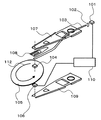
図1は、本実施の形態1に係る情報記録再生装置の構成を説明した図である。本実施の形態に係る情報再生装置は、従来の磁気ディスク装置と基本構成は類似である。近視野光を発生する微小開口(図示略)を有する近視野光ヘッド104を、記録媒体105の表面に数十nmまで近接した状態で記録媒体105を図中矢印112で示した方向に高速に回転させる。近視野光ヘッド104が記録媒体105に対して常に一定の相対配置で浮上するために、フレクシャー108をサスペンションアーム107の先端部に形成している。サスペンションアーム107はボイスコイルモータ(図示略)によって記録媒体105の半径方向に移動可能である。近視野光ヘッド104は、記録媒体105に微小開口が対面するように配置されている。レーザ101からの光束を近視野光ヘッド104に導く為に、レンズ102と、サスペンションアーム107に固定されたコアとクラッドからなる光導波路103を用いている。光導波路103は、レーザからの光束の持つ偏光方向を保存するように、コア断面形状を長方形にした偏光保存型の導波路を用いた。必要に応じて、レーザ101は回路系110により強度変調などをかけることもできる。また、記録媒体105に記録された情報を読みだす為の受光ヘッド106がサスペンションアーム109に取り付けられ、サスペンションアーム109はサスペンションアーム107と同じボイスコイルモータ(図示略)に取り付けされている。
【0031】
図2は本実施の形態1に係る情報記録再生装置の導波路と近視野光ヘッドについて説明した図である。図2のようなヘッド構造は、例えば(Kato,K.et al,International Symposium On Optical Memory 2000)において提案されている構造に類似である。基板111にはヘッド用レンズ機能を実現するために、例えば透明なガラス基板上にマイクロレンズ205を形成し、さらにその記録媒体面側に常に一定の相対配置で浮上するためにエアベアリングサーフェス204が形成されている。基板111の底面には近視野光発生素子206が形成されている。マイクロレンズ205は、光導波路103からの光束を近視野光発生素子206に集光している。
【0032】
この開口基板111の上部には、200nm厚のアルミニウム(図示略)が蒸着されたミラー面203を持つミラー基板210と、コア201とクラッド202からなる光導波路103が固定されている。ここで開口基板111として、使用するレーザの波長での光を透過するガラス基板を用いたが、シリコン基板等を用い、マイクロレンズ205と光束が透過する部分だけ使用する波長での光を透過する材料で作成してもよい。また、マイクロレンズ205は、通常の球面あるいは非球面レンズ、屈折率分布形レンズ、フレネルレンズなどを用いる事ができる。特に平面状のレンズであるフレネルレンズを用いると、径の大きなレンズを作成しても近視野光ヘッドの厚さを薄くすることが可能である。フレネルレンズは、フォトリソグラフィ技術を用いて大量生産可能である。
【0033】
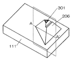
本発明は、図2で示したヘッド構造のうち、近視野光発生素子206と、入射光偏光に特徴がある。図3は本実施の形態1に係る情報記録再生装置の光ヘッドのうち、底面の近視野光発生素子206付近を示した図である。略三角錐形状の近視野光発生素子206は先端に光学的開口301を有する。図4(a)は、図3に示したA−A’平面での近視野光発生素子206付近の断面図である。図4(b)は光学的開口301付近の上面図である。
【0034】
基板111の上(底面)に二酸化ケイ素から成る高さ数μm〜10μm程度の三角錐402が形成されている。三角錐402と三角錐402付近の基板111はアルミニウムからなる遮光膜403に覆われている。遮光膜403の厚みは200〜300nm程度である。遮光膜403は三角錐402の1つの側面において、三角錐402の頂点から底辺に向かって数百nm〜数μm程度下方まで、除去されている。遮光膜403が除去された面は錐体露出部404を形作っている。遮光膜403の除去にはFIB(集束イオンビーム)装置を用いると良い。遮光膜403と錐体露出部404は、三角錐402の頂点に位置する光学的開口301を除いて、金属膜405で覆われている。金属膜405の厚みは数十nm程度であり、材料には金を用いることができる。
【0035】
図4(a)において下方から入射した光は、三角錐402の頂点に向かって伝搬する。この光は、三角錐402の中心軸を錐体露出部404面に垂直に下ろした線と三角錐402の中心軸に張る平面に平行な偏光方向を持つ。三角錐402頂点近傍の錐体露出部404に到達した前記の光は、金属膜405のプラズモンを励起し、金属膜405を介して光学的開口301に向かって伝搬する。ここで、光学的開口301から近視野光が発生する。
【0036】
錐体露出部404とそれに接する金属膜405を持たない場合、光学的開口以外の三角錐402は遮光膜のみに覆われている。入射した光は三角錐402を伝搬するが、光学的開口に近づくにつれて伝搬に寄与する領域の径が小さくなり、その径がほぼ光の波長以下になると、伝搬光は急激に減衰する(カットオフ領域)。このため、光効率が低下する。本実施の形態では、錐体露出部404とそれに接する金属膜405を有する上記構造により、カットオフ領域での光の伝搬を避けて、金属膜を介してエネルギーを光学的開口に伝搬させることができるため、従来の構造に比べて高効率な近視野光発生が可能となる。
【0037】
ここまで略三角錐形状の近視野光発生素子206について説明してきたが、他の錐体を用いて同様な効果を得ることができる。図5は略円錐形状を有する近視野光発生素子206の光学的開口付近の上面図である。図4(b)と同様に光学的開口301は錐体露出部404を除いて遮光膜403に囲まれており、かつ錐体露出部404を介して金属膜405に接している。略三角錐形状の近視野光発生素子では、FIBによる加工の際、三角錐402の側平面に平行に遮光膜403を加工する必要があるが、略円錐形状の近視野光発生素子の場合、その必要がないのは自明であり、よってその作製は容易となる。
【0038】
図6は図4のバリエーションである。構造はほぼ同様であるが、金属膜405は、錐体露出部404と錐体露出部側の側面の遮光膜403のみを覆っている点が異なる。図4の構造に比べて、金属膜405を局在させることができるため、高い記録密度に対応することが可能となる。
【0039】
(実施の形態2)
図7は本発明の実施の形態2に係る、近視野光発生素子付近の断面図である。近視野光発生素子付近以外の構成は実施の形態1と同様であり、図7は実施の形態1における図4(a)に対応する。
【0040】
基板111の上(底面)に二酸化シリコンから成る高さ数μm〜10μm程度の三角錐402が形成されている。三角錐402と三角錐402付近の基板111はアルミニウムからなる遮光膜403に覆われている。遮光膜403の厚みは200〜300nm程度である。遮光膜403は三角錐402の1つの側面において、三角錐402の頂点から底辺に向かって数百nm〜数μm程度下方まで、除去されている。三角錐402において遮光膜403が除去された部位は、数nm〜数十nm程度の深さでエッチングされている。エッチングされた面は2つの平面からなる錐体露出部404を形作っている。前記2つの平面が交わる線をエッジ701と呼ぶ。遮光膜403と錐体露出部404は、三角錐402の頂点に位置する光学的開口301を除いて、金属膜405で覆われている。金属膜405の厚みは数十nm程度であり、材料には金を用いることができる。
【0041】
光学的開口301から近視野光が発生する原理は、本発明の実施の形態1において説明した原理とほぼ同様であるが、エッジ701のために金属膜405のプラズモンがより強く励起される。
【0042】
錐体露出部404と金属膜405とエッジ701を有する上記構造により、従来の構造に比べて高効率な近視野光発生が可能となる。
【0043】
図8は図7のバリエーションである。構造はほぼ同様であるが、金属膜405は、錐体露出部404と錐体露出部側の側面の遮光膜403のみを覆っている点が異なる。図7の構造に比べて、金属膜405を局在させることができるため、高い記録密度に対応することが可能となる。
【0044】
ここまで略三角錐形状の近視野光発生素子について説明してきたが、実施の形態1と同様に、他の錐体を用いても同様な効果を得ることができる。
【0045】
(実施の形態3)
図9は本発明の実施の形態3に係る、近視野光発生素子付近の断面図である。
図9は実施の形態2における図7に対応する。
【0046】
近視野光発生素子付近以外の構成は実施の形態2と同様であるが、光学的開口を有しない点が大きく異なる。三角錐402は錐体露出部404を除いて遮光膜403に覆われ、錐体露出部404と遮光膜403の全体が金属膜405に覆われたままになっている。よって、略三角錐形状の近視野光発生素子の頂点901は金属膜405に覆われている。
【0047】
図9において下方から入射した光は、三角錐402の頂点に向かって伝搬する。この光は、三角錐402の中心軸を錐体露出部404面に垂直に下ろした線と三角錐402の中心軸に張る平面に平行な偏光方向を持つ。三角錐402頂点近傍の錐体露出部404に到達した前記の光は、金属膜405のプラズモンを励起し、金属膜405を介して頂点901に向かって伝搬する。ここで、頂点901から近視野光が発生する。
【0048】
本実施の形態では、光学的開口ではなく頂点901から近視野光が発生するため、近視野光発生素子と記録媒体105は極めて微小な領域で相互作用を生じることができる。よって、高い記録密度に対応することが可能となる。
【0049】
また、遮光膜403の全体が金属膜405に覆われているため、銀のような酸化しやすい材料を遮光膜403に用いた場合にも、遮光膜403の酸化を防ぎ、近視野光発生素子の性能劣化を防ぐことができる。
【0050】
(実施の形態4)
図10は、本発明の実施の形態4に関わる走査型近視野光顕微鏡を示す構成図である。この走査型近視野光顕微鏡は、近視野光プローブ1000と、光情報測定用の光源1001と、光源1001の前面に配置したレンズ1002と、レンズ1002で集光した光を近視野光プローブ1000まで伝搬する光ファイバ1003と、試料1010の下方に配置されたプリズム1011と、プリズム1011で反射した伝搬光を集光するレンズ1014と、集光した伝搬光を受光する光検出部1009と、を備えている。
【0051】
近視野光プローブ1000は片持ち梁1015を有しており、片持ち梁1015の先端には近視野光発生素子206を備えている。近視野光206の構造は本発明の実施の形態1から3に示したものと同様である。片持ち梁1015の近視野光発生素子206を備えた側の側面には遮光膜1016が成膜されている。
【0052】
光ファイバ1003は入射光の偏光方向を保存する偏光保存型のファイバである。また、近視野光プローブ1000の上方には、レーザ光を出力するレーザ発振器1004と、片持ち梁1015と遮光膜1016の界面で反射したレーザ光を反射するミラー1005と、反射したレーザ光を受光して光電変換する上下2分割した光電変換部1006と、を備えている。さらに、試料1010およびプリズム1011をXYZ方向に移動制御する粗動機構1013および微動機構1012と、これら粗動機構1013および微動機構1012を駆動するサーボ機構1007と、装置全体の制御をするコンピュータ1008とを備えている。
【0053】
つぎに、この走査型近視野光顕微鏡の動作について説明する。レーザ発振器1004から放出したレーザ光は、片持ち梁1015と遮光膜1016の界面で反射する。近視野光プローブ1000の片持ち梁1015は近視野光発生素子206と試料1010の表面が接近すると、試料1010との間の引力または斥力によってたわむ。このため、反射したレーザ光の光路が変化するため、これを光電変換部1006で検出する。
【0054】
光電変換部1006により検出した信号は、サーボ機構1007に送られる。サーボ機構1007は、光電変換部1006で検出した信号に基づいて、試料1010に対する近視野光プローブ1000のアプローチや、表面の観察の際に、近視野光プローブ1000のたわみが一定となるように、粗動機構1013および微動機構1012を制御する。コンピュータ1008は、サーボ機構1007の制御信号から表面形状の情報を受け取る。ま た、光源1001から放出された光は、レンズ1002により集光され、光ファイバ1003に至る。光ファイバ1003内を伝搬した光は、偏光が保存されたまま近視野光プローブ1000の近視野光発生素子206から試料1010に照射される。一方、プリズム1011により反射した試料1010の光学的情報は、レンズ1014により集光され、光検出部1009に導入される。光検出部1009の信号は、コンピュータ1008のアナログ入力インタフェースを介して取得され、コンピュータ1008により光学的情報として検出される。なお、近視野光発生素子206への光入射方法は、光ファイバ1003を用いずに、光源1001から放出された光をレンズによって直接近視野光発生素子206上へ集光して入射光を導入する方法でも良い。
【0055】
さらに、ここまで、試料1010を透過した光を検出する透過モードについて説明したが、試料1010で反射した光を検出する反射モードにおいても近視野光プローブ1000を用いることができる。また、近視野光プローブ1000をバイモルフなどで加振することによって、片持ち梁1015を振動させ、近視野光発生素子206と試料1010との間に働く斥力や引力によって生じる、片持ち梁1015の振幅の変化や、片持ち梁1015の振動の周波数変化を一定に保つように近視野光発生素子206と試料1010との距離を制御するダイナミックフォースモードでも近視野光プローブ1000を用いる事ができる。
【0056】
このような、高効率な近視野光発生が可能な近視野光発生素子206を用いた構成の走査型近視野光顕微鏡においては、実施の形態1から3に示した効果が近視野光顕微鏡においても発現し、観察画像の精度を向上させることができる。
【0057】
【発明の効果】
以上説明したように、本発明では、錐体露出部とそれに接する金属膜を有する構造により、カットオフ領域での光の伝搬を避けて、金属膜を介してエネルギーを光学的開口に伝搬させることができるため、従来の構造に比べて高効率な近視野光発生が可能となる。
【0058】
また、金属膜が錐体露出部と錐体露出部側の側面の遮光膜のみを覆う構造により、金属膜を局在させて、高い記録密度に対応することが可能となる。
【0059】
また、略円錐形状の近視野光発生素子とすることにより、FIB装置を用いた錐体露出部の形成が容易になる。
【0060】
また、本発明によれば、錐体露出部と金属膜に加えてエッジを有する上記構造により、金属膜のプラズモンがより強く励起されるため、さらに高効率な近視野光発生が可能となる。
【0061】
また、本発明では、光学的開口ではなく頂点から近視野光が発生するため、近視野光発生素子と記録媒体は極めて微小な領域で相互作用を生じることができる。よって、高い記録密度に対応することが可能となる。
【0062】
また、遮光膜の全体が金属膜に覆われているため、銀のような酸化しやすい材料を遮光膜に用いた場合にも、遮光膜の酸化を防ぎ、近視野光発生素子の性能劣化を防ぐことができる。
【0063】
また、本発明によれば、近視野光発生素子を用いた構成の走査型近視野光顕微鏡において、上記のような近視野光発生素子の効果が近視野光顕微鏡においても発現し、観察画像の精度を向上させることができる。
【図面の簡単な説明】
【図1】本発明の実施の形態1に係る情報記録再生装置の構成を説明した図である。
【図2】本発明の実施の形態1に係る情報記録再生装置の導波路と近視野光ヘッドについて説明した図である。
【図3】本発明の実施の形態1に係る情報記録再生装置の光ヘッドにおいて、底面の近視野光発生素子付近を示した図である。
【図4】本発明の実施の形態1に係る情報記録再生装置の光ヘッドにおいて、近視野光発生素子付近を示した断面図および光学的開口付近を示した上面図である。
【図5】本発明の実施の形態1に係る情報記録再生装置の光ヘッドにおいて、光学的開口付近を示した上面図である。
【図6】本発明の実施の形態1に係る情報記録再生装置の光ヘッドにおいて、近視野光発生素子付近を示した断面図である。
【図7】本発明の実施の形態2に係る情報記録再生装置の光ヘッドにおいて、近視野光発生素子付近を示した断面図である。
【図8】本発明の実施の形態2に係る情報記録再生装置の光ヘッドにおいて、近視野光発生素子付近を示した断面図である。
【図9】本発明の実施の形態3に係る情報記録再生装置の光ヘッドにおいて、近視野光発生素子付近を示した断面図である。
【図10】本発明の実施の形態4に係る顕微鏡の構成を説明した図である。
【符号の説明】
101 レーザ
102 レンズ
103 光導波路
104 近視野光ヘッド
105 記録媒体
106 受光ヘッド
107 サスペンションアーム
108 フレクシャー
109 サスペンションアーム
110 回路系
111 基板
201 コア
202 クラッド
203 ミラー面
204 エアベアリングサーフェス
205 マイクロレンズ
206 微小開口
210 ミラー基板
301 光学的開口
402 三角錐
403 遮光膜
404 錐体露出部
405 金属膜
701 エッジ
901 頂点
1001 光源
1002 レンズ
1003 光ファイバ
1004 レーザ発振器
1005 ミラー
1006 光電変換部
1007 サーボ機構
1008 コンピュータ
1009 光検出部
1010 試料
1011 プリズム
1012 微動機構
1013 粗動機構
1014 レンズ
1015 片持ち梁
1016 遮光膜[0001]
BACKGROUND OF THE INVENTION
The present invention relates to an element that generates near-field light, a head for a high-density information recording apparatus using near-field light, and a probe for a high-resolution microscope.
[0002]
[Prior art]
The near-field light generating element is used in an optical head in an optical recording apparatus that performs high-density information recording / reproduction, an optical probe in a near-field light microscope that performs observation at high resolution, and the like.
[0003]
Development of high-density optical recording devices has been actively promoted with the explosive increase in the amount of information such as images and moving images in recent years. It is known that an optical disc represented by a CD (compact disc) or a DVD (digital versatile disc) has a recording density limit due to a diffraction limit of light. In order to exceed this limit, a method using light having a shorter wavelength and a method using near-field light have been proposed. An optical recording device that uses near-field light is light that is incident on an optical microscopic aperture that is smaller than the wavelength, and the near-field light that has spread slightly from the aperture interacts with the surface of the recording medium to transmit or reflect the scattered light. In this method, a minute data mark is read by detecting light. Since the minimum mark size that can be recorded / reproduced is limited not by the wavelength of the incident light but by the aperture size, the recording density can be improved by producing a minute aperture.
[0004]
In an optical recording apparatus using near-field light, the aperture needs to be close to the surface of the recording medium. In order to realize a high data transfer rate, it is necessary to scan the surface of the recording medium at a high speed. In order to satisfy these conditions, a flying head method typically used in conventional magnetic recording has been proposed (for example, see Non-Patent Document 1). The structure of the head is such that a floating slider and a minute opening are formed on a flat substrate by a semiconductor process. For example, a silicon dioxide layer is laminated on a silicon substrate, a tip resist pattern is formed by lithography, and the silicon dioxide layer is etched to produce a conical tip made of silicon dioxide. Aluminum is vacuum-deposited to about 200 nm on this, and then the tip end is cut by a FIB (focused ion beam) apparatus to produce a tip having an optical opening at the tip.
[0005]
An optical probe used in a near-field optical microscope is manufactured by heating, extending, and cutting an optical fiber, depositing an aluminum light-shielding film, and then cutting the tip to form an optical opening.
[0006]
In the near-field light generating element as described above, efforts have been made to improve the near-field light intensity (herein referred to as the light efficiency of the probe) generated from the aperture with respect to the incident light intensity. If the probe's light efficiency is low, sufficient contrast cannot be obtained, and in the case of a near-field optical microscope, the accuracy of the output image, and in the case of a near-field optical recording device, the data transfer speed and recording density are insufficient. It is.
[0007]
In order to improve the light efficiency, a device has been devised such as flattening the tip by applying a beam from the side of the probe when the tip of the probe is cut with FIB (see, for example, Non-Patent Document 2). In addition, an attempt to improve resolution by forming minute protrusions in the opening surface (see, for example, Non-Patent Document 3) or an attempt to improve resolution by forming an edge of a light-shielding film at the base of the probe ( For example, see Non-Patent Document 4.)
[0008]
Moreover, the optical efficiency is improved by making the outline shape of the optical aperture a triangle, and making the polarization direction of incident light and one side of the triangle orthogonal to each other (see, for example, Patent Document 1).
[0009]
[Patent Document 1]
Japanese Patent Laid-Open No. 2001-118543
[Non-Patent Document 1]
Issiki, F.M. et al, Applied Physics Letters, 76 (7), 804 (2000).
[0011]
[Non-Patent Document 2]
Veerman, J.M. A. et al, Applied Physics Letters, 72 (24), 3115 (1998).
[0012]
[Non-Patent Document 3]
Ohtsu, M .; , J .; Lightwave Tech. , 13 (7), 1200 (1995)
[0013]
[Non-Patent Document 4]
Yatsui, T .; et al, Applied Physics Letters, 71 (13), 1756 (1997).
[0014]
[Problems to be solved by the invention]
However, in the methods shown in Non-Patent Document 2 or 3 and Patent Document 1, since the size of the optical aperture is less than or equal to the wavelength of light, the incident light contributes to the propagation of light as it approaches the optical aperture. When the diameter of the area to be reduced becomes smaller and the diameter is almost equal to or less than the wavelength of light, the propagating light is rapidly attenuated (cut-off area). For this reason, even if the size and shape of the optical aperture are changed, the light that has reached the optical aperture is already greatly attenuated, and the effect is limited.
[0015]
In the technique shown in Non-Patent Document 4, the above problem is addressed, but the distance between the edge of the light-shielding film and the probe tip where near-field light is generated is large, and it cannot be said that a sufficient effect is obtained. .
[0016]
The present invention is based on several attempts as described above, in order to further improve the resolution of the near-field light microscope, or the data transfer speed and recording density of the near-field optical recording apparatus, and the light of the near-field light generating element. It improves efficiency.
[0017]
[Means for Solving the Problems]
In order to solve the above-described problem, in the present invention, a near-field light generating element having an optically transparent cone and a light-shielding film covering the cone, each of the cone and the light-shielding film. A metal film covering part or all of the film, the cone exposed part on the part of the slope including the apex of the cone, the cone exposed part removed, and the cone and the metal film via the cone exposed part A near-field light generating element having contact with each other.
[0018]
As a result, it is possible to avoid the propagation of light in the cutoff region in the cone and to propagate the energy to the tip of the near-field light generating element through the metal film. Field light can be generated.
[0019]
In the near-field light generating element, the length of the cone exposed portion in the cone slope direction is from several tens of nm to the wavelength of light.
[0020]
This makes it possible to avoid the propagation of light and propagate it as energy on the metal film in an area necessary and sufficient for the size of the cut-off area.
[0021]
In the near-field light generating element, the cone exposed portion has a notch shape of the cone including the apex of the cone.
[0022]
Thereby, propagating light can be efficiently converted into energy on the metal film, and high-efficiency near-field light can be generated.
[0023]
Further, in the near-field light generating element, an optical aperture having a size equal to or less than a wavelength of light, the cone not being covered with the light shielding film and the metal film, is provided near the apex of the cone. And
[0024]
Thereby, near-field light can be efficiently generated at the tip of the near-field light generating element.
[0025]
The near-field light generating element is used in a near-field optical recording apparatus.
[0026]
This makes it possible to increase the data transfer speed and the recording density of the near-field optical recording apparatus.
[0027]
The near-field light generating element is used in a near-field light microscope.
[0028]
This makes it possible to increase the accuracy of the output image of the near-field light microscope.
[0029]
DETAILED DESCRIPTION OF THE INVENTION
Embodiments of the present invention will be described below with reference to the drawings.
[0030]
(Embodiment 1)
FIG. 1 is a diagram illustrating the configuration of the information recording / reproducing apparatus according to the first embodiment. The information reproducing apparatus according to the present embodiment is similar in basic configuration to the conventional magnetic disk apparatus. With the near-field
[0031]
FIG. 2 is a diagram for explaining the waveguide and the near-field optical head of the information recording / reproducing apparatus according to the first embodiment. The head structure as shown in FIG. 2 is similar to the structure proposed in (Kato, K. et al, International Symposium On Optical Memory 2000), for example. In order to realize the lens function for the head on the
[0032]
A
[0033]
The present invention is characterized by the near-field
[0034]
On the substrate 111 (bottom surface), a
[0035]
In FIG. 4A, light incident from below propagates toward the apex of the
[0036]
When the cone exposed
[0037]
Although the near-field
[0038]
FIG. 6 is a variation of FIG. The structure is almost the same except that the
[0039]
(Embodiment 2)
FIG. 7 is a cross-sectional view of the vicinity of a near-field light generating element according to Embodiment 2 of the present invention. The configuration other than the vicinity of the near-field light generating element is the same as that in the first embodiment, and FIG. 7 corresponds to FIG. 4A in the first embodiment.
[0040]
On the substrate 111 (bottom surface), a
[0041]
The principle that near-field light is generated from the
[0042]
With the above structure having the cone exposed
[0043]
FIG. 8 is a variation of FIG. The structure is almost the same except that the
[0044]
Although the near-triangle-pyramidal near-field light generating element has been described so far, similar effects can be obtained even when other cones are used as in the first embodiment.
[0045]
(Embodiment 3)
FIG. 9 is a cross-sectional view near the near-field light generating element according to Embodiment 3 of the present invention.
FIG. 9 corresponds to FIG. 7 in the second embodiment.
[0046]
The configuration other than the vicinity of the near-field light generating element is the same as that of the second embodiment, except that it does not have an optical aperture. The
[0047]
In FIG. 9, light incident from below propagates toward the apex of the
[0048]
In this embodiment mode, near-field light is generated not from the optical aperture but from the apex 901, so that the near-field light generating element and the
[0049]
Further, since the entire
[0050]
(Embodiment 4)
FIG. 10 is a configuration diagram showing a scanning near-field optical microscope according to the fourth embodiment of the present invention. This scanning near-field optical microscope includes a near-field
[0051]
The near-field
[0052]
The
[0053]
Next, the operation of this scanning near-field optical microscope will be described. The laser light emitted from the
[0054]
A signal detected by the
[0055]
Furthermore, although the transmission mode for detecting the light transmitted through the
[0056]
In the scanning near-field light microscope having the configuration using the near-field
[0057]
【The invention's effect】
As described above, in the present invention, energy is propagated to the optical aperture through the metal film by avoiding the propagation of light in the cut-off region by the structure having the cone exposed portion and the metal film in contact therewith. Therefore, it is possible to generate near-field light with higher efficiency than the conventional structure.
[0058]
Further, the structure in which the metal film covers only the cone-exposed portion and the light-shielding film on the side of the cone-exposed portion can localize the metal film and cope with high recording density.
[0059]
In addition, by using a substantially conical near-field light generating element, it is easy to form the cone exposed portion using the FIB apparatus.
[0060]
Further, according to the present invention, the plasmon of the metal film is more strongly excited by the above structure having the edge in addition to the cone exposed portion and the metal film, so that it is possible to generate near-field light with higher efficiency.
[0061]
In the present invention, near-field light is generated not from the optical aperture but from the apex, so that the near-field light generating element and the recording medium can interact in a very small area. Therefore, it is possible to cope with a high recording density.
[0062]
In addition, since the entire light-shielding film is covered with a metal film, even when a material that easily oxidizes, such as silver, is used for the light-shielding film, the light-shielding film is prevented from being oxidized and the performance of the near-field light generating element is deteriorated. Can be prevented.
[0063]
Further, according to the present invention, in the scanning near-field light microscope having a configuration using the near-field light generating element, the effect of the near-field light generating element as described above also appears in the near-field light microscope, Accuracy can be improved.
[Brief description of the drawings]
FIG. 1 is a diagram illustrating a configuration of an information recording / reproducing apparatus according to Embodiment 1 of the present invention.
FIG. 2 is a diagram illustrating a waveguide and a near-field optical head of the information recording / reproducing apparatus according to Embodiment 1 of the present invention.
FIG. 3 is a view showing the vicinity of a near-field light generating element on the bottom surface in the optical head of the information recording / reproducing apparatus according to Embodiment 1 of the present invention.
4 is a cross-sectional view showing the vicinity of a near-field light generating element and a top view showing the vicinity of an optical aperture in the optical head of the information recording / reproducing apparatus according to Embodiment 1 of the present invention. FIG.
FIG. 5 is a top view showing the vicinity of an optical aperture in the optical head of the information recording / reproducing apparatus according to Embodiment 1 of the present invention.
FIG. 6 is a cross-sectional view showing the vicinity of a near-field light generating element in the optical head of the information recording / reproducing apparatus according to Embodiment 1 of the present invention.
FIG. 7 is a cross-sectional view showing the vicinity of a near-field light generating element in an optical head of an information recording / reproducing apparatus according to Embodiment 2 of the present invention.
FIG. 8 is a cross-sectional view showing the vicinity of a near-field light generating element in an optical head of an information recording / reproducing apparatus according to Embodiment 2 of the present invention.
FIG. 9 is a cross-sectional view showing the vicinity of a near-field light generating element in an optical head of an information recording / reproducing apparatus according to Embodiment 3 of the present invention.
FIG. 10 is a diagram illustrating a configuration of a microscope according to a fourth embodiment of the present invention.
[Explanation of symbols]
DESCRIPTION OF
Claims (6)
前記錐体を覆う遮光膜とを有し、近視野光を発生させる近視野光発生素子であって、
前記錐体の先端部の周の一部分に載る前記遮光膜が除去された錐体露出部とを有し、
前記錐体露出部に金属膜が備えられることにより、前記錐体及び前記金属膜が接触しており、
前記遮光膜は、前記錐体露出部を除いて前記錐体を覆うことを特徴とする近視野光発生素子。An optically transparent cone located on the substrate;
A near-field light generating element that has a light-shielding film covering the cone and generates near-field light,
A cone exposed portion from which the light-shielding film placed on a portion of the circumference of the tip of the cone is removed;
By providing a metal film in the cone exposed portion, the cone and the metal film are in contact,
The near-field light generating element, wherein the light shielding film covers the cone except for the cone exposed portion.
形状となる、請求項1または2に記載の近視野光発生素子。The near-field light generating element according to claim 1, wherein the cone exposed portion has a cutout shape of the cone including the apex of the cone.
Priority Applications (1)
| Application Number | Priority Date | Filing Date | Title |
|---|---|---|---|
| JP2003003939A JP4610855B2 (en) | 2003-01-10 | 2003-01-10 | Near-field light generating element, near-field light recording device, and near-field light microscope |
Applications Claiming Priority (1)
| Application Number | Priority Date | Filing Date | Title |
|---|---|---|---|
| JP2003003939A JP4610855B2 (en) | 2003-01-10 | 2003-01-10 | Near-field light generating element, near-field light recording device, and near-field light microscope |
Related Child Applications (1)
| Application Number | Title | Priority Date | Filing Date |
|---|---|---|---|
| JP2008329442A Division JP4593666B2 (en) | 2008-12-25 | 2008-12-25 | Near-field light generating element, near-field light recording device, and near-field light microscope |
Publications (3)
| Publication Number | Publication Date |
|---|---|
| JP2004216473A JP2004216473A (en) | 2004-08-05 |
| JP2004216473A5 JP2004216473A5 (en) | 2006-01-12 |
| JP4610855B2 true JP4610855B2 (en) | 2011-01-12 |
Family
ID=32895057
Family Applications (1)
| Application Number | Title | Priority Date | Filing Date |
|---|---|---|---|
| JP2003003939A Expired - Fee Related JP4610855B2 (en) | 2003-01-10 | 2003-01-10 | Near-field light generating element, near-field light recording device, and near-field light microscope |
Country Status (1)
| Country | Link |
|---|---|
| JP (1) | JP4610855B2 (en) |
Families Citing this family (3)
| Publication number | Priority date | Publication date | Assignee | Title |
|---|---|---|---|---|
| US7489597B2 (en) | 2004-09-27 | 2009-02-10 | Sharp Kabushiki Kaisha | Electromagnetic field generating element, information recording/reproducing head, and information recording/reproducing apparatus |
| JP4710746B2 (en) * | 2005-09-28 | 2011-06-29 | コニカミノルタホールディングス株式会社 | Thermally assisted magnetic recording head and magnetic recording apparatus |
| JP5048455B2 (en) * | 2006-11-29 | 2012-10-17 | エスアイアイ・ナノテクノロジー株式会社 | Photomask defect correction apparatus and method |
-
2003
- 2003-01-10 JP JP2003003939A patent/JP4610855B2/en not_active Expired - Fee Related
Also Published As
| Publication number | Publication date |
|---|---|
| JP2004216473A (en) | 2004-08-05 |
Similar Documents
| Publication | Publication Date | Title |
|---|---|---|
| JP4094229B2 (en) | Near-field optical head and manufacturing method thereof | |
| JP4024570B2 (en) | Near-field light generating element, near-field light recording device, and near-field light microscope | |
| JP4060150B2 (en) | Micro-integrated near-field optical recording head and optical recording apparatus using the same | |
| JP4184570B2 (en) | Information recording / reproducing device | |
| KR20060065430A (en) | Optical fiber illuminator, method of fabricating the optical fiber illuminator, optical recording head, and optical recording and reading apparatus having the optical fiber illuminator | |
| JP4245117B2 (en) | Optical information recording / reproducing apparatus | |
| JP4267834B2 (en) | Information recording / reproducing device | |
| JP4421742B2 (en) | Optical head | |
| JP4601867B2 (en) | Near-field optical head | |
| JP4308731B2 (en) | Near-field optical head and information reproducing apparatus using the near-field optical head | |
| US7312445B2 (en) | Pyramid-shaped near field probe using surface plasmon wave | |
| JP4610855B2 (en) | Near-field light generating element, near-field light recording device, and near-field light microscope | |
| JP4593666B2 (en) | Near-field light generating element, near-field light recording device, and near-field light microscope | |
| EP0996122B1 (en) | Near-field optical head | |
| JP4162317B2 (en) | Near-field optical memory head | |
| JP4245118B2 (en) | Information recording / reproducing device | |
| JP4286473B2 (en) | Near-field optical head | |
| JP4482254B2 (en) | Optical head | |
| JP2000099979A (en) | Beam condensing optical device | |
| JP3892264B2 (en) | Manufacturing method of near-field light generating element | |
| JP2001110090A (en) | Recording medium and method of manufacturing the same, as well as optical information recording and reproducing device | |
| JP2006053979A (en) | Near field optical head | |
| JP2001126282A (en) | Optical information recording/reproducing device | |
| JP2001034981A (en) | Slider and flexure for information recording/ reproducing device | |
| JP2000260050A (en) | Optical recording/reproducing device |
Legal Events
| Date | Code | Title | Description |
|---|---|---|---|
| A521 | Written amendment |
Free format text: JAPANESE INTERMEDIATE CODE: A523 Effective date: 20051122 |
|
| A621 | Written request for application examination |
Free format text: JAPANESE INTERMEDIATE CODE: A621 Effective date: 20051122 |
|
| A131 | Notification of reasons for refusal |
Free format text: JAPANESE INTERMEDIATE CODE: A131 Effective date: 20080805 |
|
| A521 | Written amendment |
Free format text: JAPANESE INTERMEDIATE CODE: A523 Effective date: 20081003 |
|
| A02 | Decision of refusal |
Free format text: JAPANESE INTERMEDIATE CODE: A02 Effective date: 20081125 |
|
| A521 | Written amendment |
Free format text: JAPANESE INTERMEDIATE CODE: A523 Effective date: 20090205 |
|
| RD01 | Notification of change of attorney |
Free format text: JAPANESE INTERMEDIATE CODE: A7421 Effective date: 20091105 |
|
| RD01 | Notification of change of attorney |
Free format text: JAPANESE INTERMEDIATE CODE: A7421 Effective date: 20091112 |
|
| A521 | Written amendment |
Free format text: JAPANESE INTERMEDIATE CODE: A523 Effective date: 20100707 |
|
| A521 | Written amendment |
Free format text: JAPANESE INTERMEDIATE CODE: A523 Effective date: 20100903 |
|
| A01 | Written decision to grant a patent or to grant a registration (utility model) |
Free format text: JAPANESE INTERMEDIATE CODE: A01 |
|
| A61 | First payment of annual fees (during grant procedure) |
Free format text: JAPANESE INTERMEDIATE CODE: A61 Effective date: 20101013 |
|
| FPAY | Renewal fee payment (event date is renewal date of database) |
Free format text: PAYMENT UNTIL: 20131022 Year of fee payment: 3 |
|
| R150 | Certificate of patent or registration of utility model |
Ref document number: 4610855 Country of ref document: JP Free format text: JAPANESE INTERMEDIATE CODE: R150 Free format text: JAPANESE INTERMEDIATE CODE: R150 |
|
| R250 | Receipt of annual fees |
Free format text: JAPANESE INTERMEDIATE CODE: R250 |
|
| R250 | Receipt of annual fees |
Free format text: JAPANESE INTERMEDIATE CODE: R250 |
|
| LAPS | Cancellation because of no payment of annual fees |