JP4162317B2 - Near-field optical memory head - Google Patents
Near-field optical memory head Download PDFInfo
- Publication number
- JP4162317B2 JP4162317B2 JP05282599A JP5282599A JP4162317B2 JP 4162317 B2 JP4162317 B2 JP 4162317B2 JP 05282599 A JP05282599 A JP 05282599A JP 5282599 A JP5282599 A JP 5282599A JP 4162317 B2 JP4162317 B2 JP 4162317B2
- Authority
- JP
- Japan
- Prior art keywords
- light
- field optical
- field
- substrate
- optical memory
- Prior art date
- Legal status (The legal status is an assumption and is not a legal conclusion. Google has not performed a legal analysis and makes no representation as to the accuracy of the status listed.)
- Expired - Lifetime
Links
Images


Landscapes
- Optical Head (AREA)
- Light Receiving Elements (AREA)
- Photometry And Measurement Of Optical Pulse Characteristics (AREA)
Description
【0001】
【発明の属する技術分野】
本発明は、近視野光を利用して高密度な情報の再生を行う光メモリヘッドに関する。
【0002】
【従来の技術】
試料表面においてナノメートルオーダの微小な領域を観察するために走査型トンネル顕微鏡(STM)や原子間力顕微鏡(AFM)に代表される走査型プローブ顕微鏡(SPM)が用いられている。SPMは、先端が先鋭化されたプローブを試料表面に走査させ、プローブと試料表面との間に生じるトンネル電流や原子間力などの相互作用を観察対象として、プローブ先端形状に依存した分解能の像を得ることができるが、比較的、観察する試料に対する制約が厳しい。
【0003】
そこでいま、伝搬光を使用し、試料表面に生成される近視野光とプローブとの間に生じる相互作用を観察対象とすることで、試料表面の微小な領域の観察を可能にした近視野光学顕微鏡が注目されている。
近視野光学顕微鏡においては、伝搬光を試料の表面に照射して近視野光を生成し、生成された近視野光を先端が先鋭化されたプローブにより散乱させ、その散乱光を従来の伝搬光検出と同様に処理することで、従来の光学顕微鏡による観察分解能の限界を打破し、より微小な領域の観察を可能としている。また、試料表面に照射する光の波長を掃引することで、微小領域における試料の光学物性の観測をも可能としている。
【0004】
近視野光学顕微鏡には、光ファイバーを先鋭化して周辺を金属でコーティングすることによってその先端に微小開口を設けた光ファイバープローブを使用することが多く、光ファイバープローブを近視野光と相互作用させることによって生じた散乱光をその光ファイバープローブ内部に通過させて光検出器に導いている。
【0005】
また、光ファイバープローブを通して試料に向けて光を導入させることによって、光ファイバープローブの微小開口に近視野光を生じさせ、この近視野光と試料表面の微細構造との相互作用によって生じた散乱光を更に付加された集光系を用いて光検出器に導き、表面観察を行うことも可能である。
更に、顕微鏡としての利用だけでなく、光ファイバープローブを通して試料に向けて比較的強度の大きな光を導入させることにより、光ファイバープローブの微小開口にエネルギー密度の高い近視野光を生成し、その近視野光によって試料表面の構造または物性を局所的に変更させる高密度な光メモリ記録としての応用も可能である。
【0006】
近視野光学顕微鏡に使用されるプローブとして、例えば米国特許第5,294,790号に開示されているように、フォトリソグラフィ等の半導体製造技術によってシリコン基板にこれを貫通する開口部を形成し、シリコン基板の一方の面には絶縁膜を形成して、開口部の反対側の絶縁膜の上に円錐形状の光導波層を形成したカンチレバー型光プローブが提案されている。このカンチレバー型光プローブにおいては、開口部に光ファイバーを挿入し、光導波層の先端部以外を金属膜でコーティングすることで形成された微小開口に光を透過させることができる。
【0007】
更に、上述したプローブのように先鋭化された先端をもたない平面プローブの使用が提案されている。平面プローブは、シリコン基板に異方性エッチングによって逆ピラミッド構造の開口を形成したものであり、特にその頂点が数十ナノメートルの径を有して貫通されている。そのような平面プローブは、半導体製造技術を用いて同一基板上に複数作成すること、すなわちアレイ化が容易であり、特に近視野光を利用した光メモリの再生及び記録に適した光メモリヘッドとして使用できる。
【0008】
【発明が解決しようとする課題】
しかしながら、光ファイバープローブにおいては、先鋭化された先端を有しているために機械的強度が十分でなく、大量生産及びアレイ化にも適していない。また、近視野光を乱すことで得られる散乱光は非常に微弱であるため、光ファイバーを通してその散乱光を検出する場合には、検出部において十分な光量を得るための工夫が必要になる。また、光ファイバーを通して十分な大きさの近視野光を生成する場合には、その光ファイバーの微小開口部に光を集光する工夫が必要となる。
【0009】
また、カンチレバー型光プローブにおいては、その開口部に光ファイバーを挿入して、光導波層からの散乱光の受光、または光導波層への伝搬光の導入を達成するため、光導波層と光ファイバーとの間において十分な光量を損失なく伝搬することができなかった。
カンチレバー型光プローブは、アレイ化、特に2次元に配列するアレイ化の実現は困難である。また、これらは元来、顕微鏡としての利用を目的としているために光メモリの情報記録・再生を念頭においてはおらず、記録媒体上の高速な掃引は困難である。
【0010】
更に、光ファイバープローブ、カンチレバー型光プローブ及び平面プローブを光メモリヘッドとして記録媒体上に記録された情報を再生するために用いた場合には、これらプローブは記録媒体に近視野光を生成させる近視野光生成用、または、生成された近視野光を散乱させてその散乱光を光検出器に導く近視野光検出用のどちらか一方に対してのみに利用されるのが通例であり、プローブのみの構成で情報再生を実現することは困難であった。
【0011】
また、平面プローブに至っては、微小開口を記録媒体に近接させた状態において、微小開口近傍と記録媒体との間に十分な空間を有していないため、記録媒体表面に向けて光を照射することにより同じく記録媒体の表面に近視野光を生じさせる反射型の近視野光を利用することができなかった。
従って、本発明は、近視野光を利用した光メモリに記録された情報の再生を実現させるために、コンパクトな構成かつ大量生産及びアレイ化に適した近視野光メモリヘッドを提供することを目的とする。
【0012】
【課題を解決するための手段】
上記の目的を達成するために、近視野光を利用して記録媒体の情報の再生を行う近視野光メモリヘッドであって、少なくとも1つの光源と、前記光源からの光束を記録媒体に照射するためのレンズと、少なくとも1つの逆錐状の穴がその頂部を微小開口とするように貫通して形成された微小開口を有する平面基板と、前記逆錐状の穴の上部に形成された受光素子と、前記光源からの光束を遮光する為の遮光膜と、を含み、前記少なくとも1つの光源は、少なくとも前記平面基板を透過する波長成分をもち、前記光源からの照射光を前記遮光膜で遮光し、前記微小開口からの伝搬光を前記受光素子が受光する。
【0013】
従って、平面基板は光源からの光束の一部あるいは全てを透過し、この透過した透過光成分により記録媒体表面に光を照射することにより記録媒体表面に近視野光が生成され、生成された近視野光と微小開口との相互作用によって生じる伝搬光の取り出しが、同一の基板上において実現できる。
また、本発明に係る近視野光メモリヘッドは、近視野光を利用して記録媒体の情報の再生を行う近視野光メモリヘッドにおいて、少なくとも赤外光成分を含む光源と、前記光源からの光束を記録媒体に照射するためのレンズと、少なくとも1つの逆錐状の穴がその頂部を微小開口とするように貫通して形成された微小開口を有する平面基板と、前記逆錐状の穴の上部に形成された受光素子と、前記光源からの光束を遮光する為の遮光膜と、を含み、前記微小開口を有する平面基板は、赤外光成分を透過することができるSiやGaAs等の半導体基板であり、前記光源からの照射光を前記遮光膜で遮光し、前記微小開口からの伝搬光を前記受光素子が受光する。
【0014】
従って、平面基板は赤外光成分を透過し、この透過した赤外光成分により記録媒体表面に光を照射することにより記録媒体表面に近視野光が生成され、生成された近視野光と微小開口との相互作用によって生じる伝搬光の取り出しが、同一の基板上において実現できる。
更に、本発明に係る近視野光メモリヘッドは、前記受光素子は、前記微小開口を有する平面基板とは別の平面基板上に形成され、前記微小開口を有する平面基板上部に受光素子を下にして配置されている。
【0015】
従って、受光素子を基板上に作成する過程と、平面基板に微小開口を作成する過程とを分離し、それらを合わせる事により容易に近視野光ヘッドを実現出来る。
更に、本発明に係る近視野光メモリヘッドは、前記受光素子が、平面基板上に形成された少なくとも1つの受光素子と、前記受光素子上部に形成された錐状の突起部と、前記受光素子と前記錐状の突起部を包み込むように形成された遮光膜とを含み、光源が少なくとも前記平面基板および前記錘状突起部を透過する波長成分をもち、前記遮光膜に前記錐状の突起部頂部の上部に微小開口をもうけ、この微小開口が形成された平面基板は前記微小開口が前記記録媒体に面して配置されている。
【0016】
従って、平面基板は光源からの光束の一部あるいは全てを透過し、この透過した透過光により記録媒体表面に光を照射することにより記録媒体表面に近視野光が生成され、生成された近視野光と微小開口との相互作用によって生じる伝搬光の取り出しが、同一の基板上において実現できる。
更に、本発明に係る近視野光メモリヘッドは、前記受光素子が、平面基板上に形成された少なくとも1つの受光素子と、前記受光素子上部に形成された赤外光を透過する錐状の突起部と、前記受光素子と前記錐状の突起部を包み込むように形成された遮光膜とを含み、前記遮光膜に前記錐状の突起部頂部の上部に微小開口をもうけ、この微小開口が形成された平面基板は前記微小開口が前記記録媒体に面して配置されている。
【0017】
従って、平面基板は赤外光成分を透過し、この透過した赤外光により記録媒体表面に光を照射することにより記録媒体表面に近視野光が生成され、生成された近視野光と微小開口との相互作用によって生じる伝搬光の取り出しが、同一の基板上において実現できる。その上、1枚の平面基板上に近視野光メモリヘッドを半導体プロセスで作成することができる。
【0018】
更に、本発明に係る近視野光メモリヘッドは、前記レンズを前記微小開口を有する平面基板上に、レンズ効果を有する屈折率分布型レンズや回折格子等とし、一体化する。従って、レンズまで含めた近視野光ヘッドの小型が容易に実現できる。
【0019】
【発明の実施の形態】
以下に、本発明に係る近視野光メモリヘッドの実施の形態を図面に基づいて詳細に説明する。
[実施の形態1]
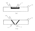
図1は、実施の形態1に係る近視野光メモリヘッドの断面図を示している。また、図2は図1中の近視野光ヘッド部4のみの断面図である。
【0020】
赤外光成分を含む光源1からの光束は、コリメーターレンズ2で平行光束になり、レンズ3を用いて近視野光ヘッド部4に照射される。シリコン基板は赤外光成分に対して非常に透過率が高く、光源1からの赤外光成分はシリコン基板9を透過し、記録媒体5上に照射される。そして、記録媒体5の表面に近視野光が生成される。
【0021】
図2に示した近視野光ヘッド部4において、シリコン基板9にはこれを貫通するテーパ開口部13が微小開口12を有して形成されている。微小開口12は、微小開口12の近傍に生じている近視野光と相互作用を起こし、その結果得られる伝搬光8を取り出せるように、例えば数十ナノメートルの径を有している。さらに、テーパ開口部13の上部には、受光素子10が取り付けられている。そして、テーパ開口部13の表面と受光素子10には、光源1からの照射光6を受光素子10から光学的に閉塞するために遮光膜11が形成されている。
【0022】
テーパ開口部13は、例えば半導体製造プロセスにおけるフォトリソグラフィやシリコン異方性エッチングなどを用いた微細加工によって形成される。また、光源1はシリコン基板9を透過できる赤外光成分を含んでいる。遮光膜11は、例えばAu/Cr等の金属膜であり、スパッタリングや真空蒸着によって得られる。この遮光膜は、光源1の持つ波長成分に対して、十分な遮光性がえられるものであれば干渉を用いた薄膜多層膜でもよい。
【0023】
次に、以上に説明した近視野光ヘッド部4を記録媒体5上に配置し、微小開口12において情報再生を行う方法を説明する。
ここで記録媒体5は、例えば円盤状の平面基板であり、その上面に近視野光ヘッド部4が配置される。近視野光ヘッド部4の微小開口12と記録媒体5表面に生じている近視野光とを相互作用させるために、微小開口12と記録媒体5との間を微小開口12の径程度まで近接させる必要がある。そこで、近視野光ヘッド部4と記録媒体5との間に潤滑剤を充填し、近視野光メモリヘッドを十分に薄く形成することで、潤滑剤の表面張力を利用して近視野光ヘッド部4と記録媒体5との間隔を十分に小さく維持できる。更には、記録媒体5の撓みに対しても追従できる。また、図示しない近視野光メモリヘッド制御機構によって、微小開口12を記録媒体5上の所望の位置に配置できるように近視野光ヘッド部4の位置を制御できる。
【0024】
なお、近視野光ヘッド部4と記録媒体5との近接状態を、上記した潤滑剤によらずに、ハードディスク技術に用いられているフライングヘッドと同様にエアベアリングによって制御したり、近視野光学顕微鏡に用いられるAFM制御を行っても同様の作用が得られる。
記録媒体に記録された情報の再生は、先ず、上記した制御により、微小開口12を記録媒体5上の所望の情報再生位置に移動させる。そして、光源1から出射されたシリコン基板9を透過する赤外光成分は、コリメーターレンズ2およびレンズ3を用いて、再生位置となる微小開口12に近接した記録媒体5の情報記録部を照射し、その情報記録部において近視野光が生成される。この近視野光と遮光膜が付けられたテーパ開口部13の先端である微小開口12との相互作用によって、その情報記録部の記録状態に依存した強度や位相等の特性を伴った伝搬光8が、微小開口12を介してテーパ開口部13上方へと取り出される。取り出された伝搬光8は、受光素子10へと導かれて電気信号に変換され、図示しない信号処理部によって情報記録部の記録状態が判断される。その際、遮光膜11により受光素子10に微小開口12からの伝搬光8以外の光が受光されないよう構成されている。
【0025】
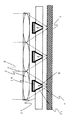
更に、近視野光ヘッド部4は、従来の半導体製造プロセスによって形成できるため、近視野光ヘッド部4を同一シリコン基盤上に複数個配列させることが容易となる。図6に近視野光メモリヘッドアレイを示す。光源は複数個のレーザー等や、面発光レーザーのような1チップ上に複数個の光源が作製されたものを用いることも可能である。あるいは、1つの光源と複数のミラーを用いて光束を分けても同様の作用が得られる。このような近視野光メモリヘッドアレイを、同心円状の複数のトラック上に情報を記録した記録媒体上に近接させ、近視野光メモリヘッドアレイがその記録媒体の複数のトラック上に位置するように配置することによって、記録媒体上におけるヘッドの掃引を最小限に抑え、トラッキング制御を必要としない高速な光記録または再生が可能となる。
【0026】
以上説明したように、実施の形態1によれば、近視野光を利用することによって再生可能な、かつ高密度に情報が記録された記録媒体において、その記録された情報の再生を行うのに、記録媒体に近視野光を生成させる近視野光生成系、及び、生成された近視野光と相互作用して得られる伝搬光を受光素子に導く近視野光検出系を一体化した近視野光メモリヘッドが提供され、光メモリ装置全体の構成をコンパクトにし、各構成要素の調整を不必要にしている。
【0027】
更に、本発明に係る近視野光メモリヘッドは、半導体製造プロセスを用いて形成できるため、大量生産に適しており、近視野光メモリヘッドのアレイ化に対応できる。
また、本発明に於いて、シリコン基板を用いたが、GaAs等の他の半導体基板を用いても同様の効果がえられることは言うまでもない。
【0028】
[実施の形態2]
図3は、実施の形態2に係る近視野光メモリヘッドにおける近視野光ヘッド部の断面図を示している。なお、図2と共通する部分には同一符号を付している。また、実施の形態1と同じ箇所については、説明を簡略化、あるいは省略する。図3の近視野光メモリ部は、図1における実施の形態1に係る近視野光ヘッド部4と完全に置き換えられる。この図3の近視野光ヘッド部は、シリコン基板A14とシリコン基板B16の2枚からなる。図4に、それぞれのシリコン基板の分解図を示す。
【0029】
図4−Aのシリコン基板A14は、これを貫通するテーパ開口部13が微小開口12を有して形成されている。微小開口12は、記録媒体5表面に生成された近視野光と相互作用を起こし、その結果得られる伝搬光8を取り出せるように、例えば数十ナノメートルの径を有している。そして、テーパ開口部13の表面には、光源1からの照射光6から光学的に閉塞するために遮光膜15が形成されている。
【0030】
図4−Bのシリコン基板B16は、遮光膜18と受光素子17が形成出来る分だけ、シリコン基板を加工し、その上に遮光膜18をほどこし、最後に受光素子17を形成している。
そして、シリコン基板B16を上下反転させ、シリコン基板A14と重ね合せる。その際、遮光膜15と遮光膜18により、光源1からの照射光6から受光素子17を光学的に閉塞するできるように位置合せ等をする必要がある。
【0031】
テーパ開口部13は、例えば半導体製造プロセスにおけるフォトリソグラフィやシリコン異方性エッチングなどを用いた微細加工によって形成される。また、光源1はシリコン基板A14及びシリコン基板B16を透過できる赤外光成分を含んでいる。遮光膜15および遮光膜18は、例えばAu/Cr等の金属膜であり、スパッタリングや真空蒸着によって得られる。これらの遮光膜は、光源1の光成分に対して、十分な遮光性がえられるものであれば干渉を用いた薄膜等でも同様の効果が得られる。
【0032】
以上に説明した近視野光ヘッド部を記録媒体5上に配置し、微小開口12において情報再生を行う方法は、実施の形態1と全く同じであるので、説明を省略する。
上述した実施の形態2において、近視野光メモリ部は半導体製造プロセスを用いて形成でき、2枚のシリコン基板を張り合わせることにより作成できるため、大量生産に適しており、実施の形態1において説明されたようなアレイ化にも容易に対応でき、近視野光メモリヘッドアレイとしての使用が可能である。
【0033】
また、本発明に於いて、シリコン基板を用いたが、GaAs等の他の半導体基板を用いても同様の効果がえられることは言うまでもない。
[実施の形態3]
図5は、実施の形態3に係る近視野光メモリヘッドにおける近視野光ヘッド部の断面図を示している。また、実施の形態1および実施の形態2と同じ箇所については、説明を簡略化、あるいは省略する。
【0034】
図5の近視野光ヘッド部は、図1における実施の形態1に係る近視野光ヘッド部4と完全に置き換えられる。
この図5の近視野光ヘッド部は、シリコン基板19上に、下部遮光膜21を作成し、受光素子20をその下部遮光膜21の上に作成する。その後この受光素子20上に錐状突起部24を作成する。そして、最後に上部遮光膜22を作成し、錐状突起部24の上部の上部遮光膜22に微小開口23を作成する。微小開口23は、実施の形態1と同様な大きさの径を有している。
【0035】
このような微小開口が形成された平面基板である近視野光ヘッド部は、微小開口23が記録媒体5側になるように上下反転させ、近視野光メモリヘッドを構成する。
また、下部遮光膜21及び上部遮光膜22は、例えばAu/Cr等の金属膜であり、スパッタリングや真空蒸着によって得られる。これらの遮光膜は、光源1の光成分に対して、十分な遮光性がえられるものであれば干渉を用いた薄膜等でも同様の効果が得られる。錐状突起部24は、例えばSiO2であり、半導体製造プロセスにおけるフォトリソグラフィやシリコン異方性エッチングなどを用いた微細加工によって形成される。この錐状突起部24は、赤外光成分を透過すれば良く、赤外光成分を透過する他の材料でも可能である。
【0036】
以上に説明した近視野光ヘッド部を記録媒体5上に配置し、微小開口23において情報再生を行う方法は、実施の形態1と全く同じであるので、説明を一部省略あるいは簡単にする。
記録媒体に記録された情報の再生は、先ず、微小開口23を記録媒体5上の所望の情報再生位置に移動させる。そして、光源1から出射されたシリコン基板9を透過する赤外光成分は、再生位置となる微小開口23に近接した記録媒体5の情報記録部を照射し、その情報記録部において近視野光が生成される。この近視野光と遮光膜が付けられた錐状突起部24の先端である微小開口23との相互作用によって、その情報記録部の記録状態に依存した強度や位相等の特性を伴った伝搬光8が、微小開口23を介して錐状突起部24上方へと取り出される。取り出された伝搬光8は、受光素子20へと導かれて電気信号に変換され、図示しない信号処理部によって情報記録部の記録状態が判断される。その際、上部遮光膜21及び下部遮光膜22により受光素子20に微小開口23からの伝搬光8以外の光が受光されないよう構成されている。
【0037】
上述した実施の形態3において、近視野光メモリ部は半導体製造プロセスを用いて形成でき、1枚のシリコン基板をより作成できるため、大量生産に適しており、実施の形態1において説明されたようなアレイ化にも容易に対応でき、近視野光メモリヘッドアレイとしての使用が可能である。
また、本発明に於いて、シリコン基板を用いたが、GaAs等の他の半導体基板を用いても同様の効果がえられることは言うまでもない。
【0038】
[実施の形態4]
図7は、実施の形態4に係る近視野光メモリヘッドの断面図を示している。なお、本実施例は、実施の形態2におけるレンズ3と近視野光ヘッド部を一体化させたものであるので共通する部分には同一符号を付している。この図7の近視野光メモリヘッドは、シリコン基板A14とシリコン基板B16とガラス基板27からなる。これらの基板の分解図を図8に示す、
実施の形態4は、実施の形態2のシリコン基板A14とシリコン基板B16の更に上部に、屈折率分布レンズ28を有するガラス基板27を重ねて一体化している。屈折率分布レンズ28を有するガラス基板27を用いることで、実施の形態2のレンズ3を省略することができる。
【0039】
以上に説明した近視野光メモリヘッドを記録媒体5上に配置し、微小開口12において情報再生を行う方法は、実施の形態1と同じであるので、説明を一部省略あるいは簡単にする。
記録媒体に記録された情報の再生は、先ず、微小開口12を記録媒体5上の所望の情報再生位置に移動させる。ガラス基板とシリコン基板A14およびシリコン基板B16は赤外光成分を透過するので、光源1から出射された赤外光成分は、ガラス基板27に形成された屈折率分布レンズ28により、再生位置となる微小開口12に近接した記録媒体5の情報記録部を照射する。そして、その情報記録部において近視野光が生成される。この近視野光と遮光膜15が付けられたテーパ開口部13の先端である微小開口12との相互作用によって、その情報記録部の記録状態に依存した強度や位相等の特性を伴った伝搬光8が、微小開口12を介してテーパ開口部13上方へと取り出される。取り出された伝搬光8は、受光素子17へと導かれて電気信号に変換され、図示しない信号処理部によって情報記録部の記録状態が判断される。その際、遮光膜18により受光素子17に微小開口12からの伝搬光8以外の光が受光されないよう構成されている。
【0040】
このような近視野光メモリヘッドは半導体製造プロセスを用いて形成できるため、大量生産に適しており、実施の形態1及び2等において説明されたようなアレイ化に対応でき、近視野光メモリヘッドアレイとしての使用が可能である。
例として、図9に、本実施の形態4における近視野光メモリヘッドをアレイ状に配列した近視野光メモリヘッドアレイを示す。
【0041】
また、屈折率レンズ28は、回折格子等のレンズ効果を有するものを用いても良いことは言うまでもない。
[実施の形態5]
図10は、実施の形態5に係る近視野光メモリヘッドの断面図を示している。なお、本実施例は、実施例の形態4と同様に、実施の形態1におけるレンズ3と近視野光ヘッド部4を一体化させたものであるので共通する部分には同一符号を付している。
【0042】
実施の形態1で説明した近視野光ヘッド部とレンズ3を一体化するために、図1の近視野光ヘッド部4に於いて、遮光膜11を施した受光素子10の近傍に回折格子29を配置した。この回折格子29は、微小開口近傍に照射光6を照射するように回折格子が設計されている。そしてこの回折格子29により照射光6が記録媒体5に照射され、記録媒体5表面に近視野光が生成される。そして、この近視野光と微小開口との相互作用による伝搬光8を受光素子10で受光する。回折格子29は、例えば半導体製造プロセスにおけるフォトリソグラフィやシリコン異方性エッチングなどを用いた微細加工によって形成される。
【0043】
記録媒体に記録された情報の再生は、先ず、微小開口12を記録媒体5上の所望の情報再生位置に移動させる。シリコン基板は赤外光成分を透過するので、光源1から出射された赤外光成分は、遮光膜11がほどこされた受光素子10近傍に形成された回折格子29により、再生位置となる微小開口に近接した記録媒体5の情報記録部を照射する。そして、その情報記録部において近視野光が生成される。この近視野光と遮光膜11が付けられたテーパ開口部13の先端である微小開口12との相互作用によって、その情報記録部の記録状態に依存した強度や位相等の特性を伴った伝搬光8が、微小開口を介して受光素子10へと導かれて電気信号に変換され、図示しない信号処理部によって情報記録部の記録状態が判断される。その際、遮光膜11により受光素子10に微小開口からの伝搬光8以外の光が受光されないよう構成されている。
【0044】
さらに、以上に説明した近視野光メモリヘッドは回折格子を含め半導体製造プロセスを用いて形成できるため、大量生産に適しており、実施の形態1及び2において説明されたようなアレイ化に対応でき、近視野光メモリヘッドアレイとしての使用が可能である。
例として、図11に、近視野光メモリヘッドをアレイ状に配列した近視野光メモリヘッドアレイを示している。
【0045】
以上説明したように、実施の形態5によれば、記録媒体に反射型の近視野光を生成させる近視野光生成系、及び、生成された近視野光と相互作用して得られる伝搬光を受光素子に導く近視野光検出系を一体化した近視野光メモリヘッドが提供される。そして構成が簡単なため、複雑な製造過程を必要とせず、光メモリ装置全体の構成をコンパクトにし、各構成要素の調整を不必要にしている。
【0046】
[実施の形態6]
図1及び図2の実施の形態1に於いて、平面基板として、シリコン基板9の代わりにBK7等のガラス基板を用い、光源1としてガラス基板に対して十分透過率が高い波長成分(例えば、可視光)を含む光源を用い、光源1からの照射光6を受光素子10から光学的に閉塞するために遮光膜11が形成されている構造とした。微小開口12は、微小開口12の近傍に生じている近視野光と相互作用を起こし、その結果得られる伝搬光8を取り出せるように、例えば数十ナノメートルの径を有している。他の部分は実施の形態1と同じである。
【0047】
テーパ開口部13は、例えば、機械的微細加工や、ガラス基板を加熱し軟化させ、あらかじめ作成しておいた錘状の型形状を転写させることで形成される。また、光源1はガラス基板を透過出来る可視光成分を含んでいる。遮光膜は、実施の形態1と同様に例えばAu/Cr等の金属膜であり、スパッタリングや真空蒸着によって得られる。この遮光膜は、光源1の持つ波長成分に対して、十分な遮光性が得られるものであれば干渉を用いた薄膜多層膜でもよい。
【0048】
以上説明した近視野光ヘッド部を記録媒体5上に配置し、微小開口12において情報を再生を行う方法は、光源に用いる波長成分が異なる点と平面基板の材質が異なる点を除き実施の形態1と全く同じであるので、説明を省略する。
上述した実施の形態6に於いて、実施の形態1と同様に、近視野光を利用することによって再生可能な、かつ高密度に情報が記録された記録媒体において、その記録された情報の再生を行うのに、記録媒体に近視野光を生成させる近視野光生成系、及び、生成された近視野光と相互作用して得られる伝搬光を受光素子に導く近視野光検出系を一体化した近視野光メモリヘッドが提供され、光メモリ装置全体の構成をコンパクトにし、各構成要素の調整を不必要にしている。
【0049】
さらに、波長として赤外光よりも短い波長成分をもつ光源を用いることができるので、微小開口12からの伝搬光8の光強度が強くなり、受光素子10上で得られる光強度が大きくなる。その上、実施の形態1において説明されているようなアレイ化にも対応でき、近視野光メモリヘッドアレイとしての使用が可能である。
【0050】
また、実施の形態2から実施の形態5においても実施の形態6と同様に、平面基板としてシリコン基板の代わりにBK7等のガラス基板を用い、光源1としてガラス基板に対して十分透過率が高い波長(例えば、可視光)を含む光源を用いた場合についても適用でき、それぞれの実施の形態において同様な効果を得ることができる。
【0051】
上記説明において、平面基板としてガラス基板を用いたが、ポリメチルメタクリエート(PMMA)等のプラスティックやTiO2等の光学結晶等を用いても同様の効果が得られる。つまり、光源のもつ波長帯域あるいは波長成分が、平面基板を透過する波長成分を含んでいればよく、ある波長に対して透過率が十分に高い平面基板と、その波長成分を含む光源とを用いることで、上記説明した平面基板の材質以外でも実施可能である。
【0052】
【発明の効果】
以上説明したように本発明によれば、記録媒体上に近視野光を生成させる近視野光生成系、及び、生成された近視野光と相互作用して得られる伝搬光を受光素子に導く近視野光検出系、更には受光素子まで一体化している。
このため、光メモリ装置全体の構成をコンパクトにし、各構成要素の調整が不必要となる。また、ヘッドのアレイ化の実現も容易に行える。
【0053】
さらに、近視野光メモリヘッドを複雑な製造過程を必要とせずに作成できるので、特に平面基板にシリコン基板を用いた場合には半導体プロセスをもちいて作成でき、低コストで大量生産が可能である。
【図面の簡単な説明】
【図1】本発明の実施の形態1による近視野光メモリヘッドの断面図である。
【図2】本発明の実施の形態1による近視野光ヘッド部の断面図である。
【図3】本発明の実施の形態2による他の近視野光ヘッド部の断面図である
【図4】本発明の実施の形態2による他の近視野光ヘッド部の分解図である。
【図5】本発明の実施の形態3による他の近視野光ヘッド部の断面図である。
【図6】本発明の実施の形態1による近視野光メモリヘッドのアレイ化を説明する図である。
【図7】本発明の実施の形態4による近視野光メモリヘッドの断面図である。
【図8】本発明の実施の形態4による近視野光メモリヘッドの分解図である。
【図9】本発明の実施の形態5による近視野光メモリヘッドのアレイ化を説明する図である。
【図10】本発明の実施の形態5による近視野光メモリヘッドの断面図である。
【図11】本発明の実施の形態5による近視野光メモリヘッドのアレイ化を説明する図である。
【符号の説明】
1 光源
2 コリメーターレンズ
3 レンズ
4 近視野光ヘッド部
5 記録媒体
6、7 照射光
8 伝搬光
9、19、25 シリコン基板
10、17、20 受光素子
11、15、18 遮光膜
12 微小開口
13 テーパ開口部
14 シリコン基板A
16 シリコン基板B
21 下部遮光膜
22 上部遮光膜
23 微小開口
24 錐状突起部
26 近視野光メモリヘッド
27 ガラス基板
28 屈折率分布レンズ
29 回折格子[0001]
BACKGROUND OF THE INVENTION
The present invention relates to an optical memory head that reproduces high-density information using near-field light.
[0002]
[Prior art]
A scanning probe microscope (SPM) typified by a scanning tunneling microscope (STM) or an atomic force microscope (AFM) is used to observe a minute region on the order of nanometers on the sample surface. SPM scans a sample surface with a probe with a sharpened tip, and observes the interaction between the probe and the sample surface, such as tunneling current and atomic force, with an image of resolution depending on the probe tip shape. However, restrictions on the sample to be observed are relatively severe.
[0003]
Therefore, near-field optics that enables observation of minute regions on the sample surface by using the propagation light and observing the interaction between the near-field light generated on the sample surface and the probe. Microscopes are attracting attention.
In a near-field optical microscope, the near-field light is generated by irradiating the surface of the sample with propagating light, and the generated near-field light is scattered by a probe with a sharpened tip. By processing in the same manner as the detection, the limit of the observation resolution by the conventional optical microscope is overcome, and it is possible to observe a finer region. In addition, it is possible to observe the optical properties of the sample in a minute region by sweeping the wavelength of the light applied to the sample surface.
[0004]
Near-field optical microscopes often use an optical fiber probe that has a sharp aperture and is coated with metal around it to provide a microscopic aperture at the tip of the optical microscope. This occurs when the optical fiber probe interacts with near-field light. The scattered light passed through the optical fiber probe is guided to the photodetector.
[0005]
Also, by introducing light toward the sample through the optical fiber probe, near-field light is generated at the microscopic aperture of the optical fiber probe, and the scattered light generated by the interaction between the near-field light and the fine structure of the sample surface is further reduced. It is also possible to conduct surface observation by guiding the light to the photodetector using the added light collection system.
Furthermore, not only as a microscope, but also by introducing relatively high intensity light toward the sample through the optical fiber probe, near-field light with high energy density is generated at the microscopic aperture of the optical fiber probe. Therefore, it can be applied as a high-density optical memory recording that locally changes the structure or physical properties of the sample surface.
[0006]
As a probe used in a near-field optical microscope, for example, as disclosed in US Pat. No. 5,294,790, an opening is formed in a silicon substrate by a semiconductor manufacturing technique such as photolithography, and one of the silicon substrates is formed. There has been proposed a cantilever type optical probe in which an insulating film is formed on the surface and a conical optical waveguide layer is formed on the insulating film opposite to the opening. In this cantilever type optical probe, light can be transmitted through a minute opening formed by inserting an optical fiber into the opening and coating the portion other than the tip of the optical waveguide layer with a metal film.
[0007]
Furthermore, it has been proposed to use a planar probe that does not have a sharpened tip like the above-described probe. The planar probe is formed by forming an opening of an inverted pyramid structure on a silicon substrate by anisotropic etching, and its apex is penetrated with a diameter of several tens of nanometers. A plurality of such planar probes can be formed on the same substrate using semiconductor manufacturing technology, that is, can be easily arrayed, and can be used as an optical memory head suitable for reproducing and recording an optical memory using near-field light. .
[0008]
[Problems to be solved by the invention]
However, since the optical fiber probe has a sharpened tip, the mechanical strength is not sufficient, and it is not suitable for mass production and arraying. Moreover, since the scattered light obtained by disturbing near-field light is very weak, when detecting the scattered light through an optical fiber, a device for obtaining a sufficient amount of light is required in the detection unit. In addition, when near-field light having a sufficiently large size is generated through an optical fiber, it is necessary to devise a method for condensing the light at a minute opening of the optical fiber.
[0009]
Further, in the cantilever type optical probe, an optical fiber is inserted into the opening to receive the scattered light from the optical waveguide layer or introduce the propagation light into the optical waveguide layer. It was not possible to propagate a sufficient amount of light without loss.
The cantilever type optical probe is difficult to realize an array, in particular, an array arranged in two dimensions. Also, since these are originally intended for use as a microscope, information recording / reproduction of the optical memory is not considered, and high-speed sweeping on the recording medium is difficult.
[0010]
Furthermore, when an optical fiber probe, a cantilever type optical probe, and a planar probe are used as an optical memory head to reproduce information recorded on a recording medium, these probes generate near-field light that generates near-field light on the recording medium. This is usually used only for generating or for detecting near-field light that scatters the generated near-field light and guides the scattered light to a photodetector. It was difficult to realize information reproduction with the configuration.
[0011]
In addition, in the state where the flat probe is brought close to the recording medium, since there is not enough space between the vicinity of the fine opening and the recording medium, light is irradiated toward the surface of the recording medium. Accordingly, it has been impossible to use the reflection type near-field light that generates near-field light on the surface of the recording medium.
Accordingly, an object of the present invention is to provide a near-field optical memory head that is compact and suitable for mass production and arraying in order to realize reproduction of information recorded in an optical memory using near-field light. .
[0012]
[Means for Solving the Problems]
In order to achieve the above object, a near-field optical memory head for reproducing information on a recording medium using near-field light for irradiating the recording medium with at least one light source and a light beam from the light source A flat substrate having a microscopic aperture formed by penetrating at least one inverted conical hole so that the top of the lens has a microscopic aperture, and a light receiving element formed above the inverted conical hole And a light shielding film for shielding light flux from the light source, wherein the at least one light source has a wavelength component that transmits at least the planar substrate, and the light emitted from the light source is shielded by the light shielding film. The light receiving element receives the propagation light from the minute aperture.
[0013]
Accordingly, the flat substrate transmits part or all of the light flux from the light source, and the near-field light is generated on the surface of the recording medium by irradiating the recording medium surface with the transmitted light component. Extraction of propagation light generated by the interaction between the field light and the minute aperture can be realized on the same substrate.
A near-field optical memory head according to the present invention is a near-field optical memory head that reproduces information on a recording medium using near-field light, and records a light source including at least an infrared light component and a light flux from the light source. A lens for irradiating the medium, a planar substrate having a minute opening formed so that at least one inverted conical hole has a minute opening at the top, and an upper part of the inverted conical hole; A planar substrate including the formed light receiving element and a light shielding film for shielding a light beam from the light source, and the planar substrate having the minute aperture is a semiconductor substrate such as Si or GaAs capable of transmitting an infrared light component The irradiation light from the light source is shielded by the light shielding film, and the light receiving element receives the propagation light from the minute aperture.
[0014]
Therefore, the planar substrate transmits an infrared light component, and the transmitted infrared light component irradiates light on the surface of the recording medium, thereby generating near-field light on the surface of the recording medium. Extraction of propagating light generated by the interaction with the aperture can be realized on the same substrate.
Furthermore, in the near-field optical memory head according to the present invention, the light receiving element is formed on a flat substrate different from the flat substrate having the minute opening, and the light receiving element is placed on the flat substrate having the minute opening. Has been placed.
[0015]
Therefore, the process of creating the light receiving element on the substrate and the process of creating the minute aperture on the flat substrate are separated, and a near-field optical head can be easily realized by combining them.
Furthermore, in the near-field optical memory head according to the present invention, the light receiving element includes at least one light receiving element formed on a flat substrate, a cone-shaped protrusion formed on the light receiving element, and the light receiving element. A light shielding film formed so as to wrap around the cone-shaped protrusion, and a light source has a wavelength component that transmits at least the planar substrate and the weight-shaped protrusion, and the top of the cone-shaped protrusion is formed on the light-shielding film. The flat substrate on which the minute opening is formed is arranged so that the minute opening faces the recording medium.
[0016]
Therefore, the flat substrate transmits a part or all of the light flux from the light source, and the near-field light is generated on the surface of the recording medium by irradiating the surface of the recording medium with the transmitted light. Extraction of propagating light generated by the interaction between light and a minute aperture can be realized on the same substrate.
Furthermore, in the near-field optical memory head according to the present invention, the light receiving element has at least one light receiving element formed on a flat substrate, and a cone-shaped protrusion that transmits infrared light formed on the light receiving element. And a light-shielding film formed so as to wrap around the light-receiving element and the cone-shaped projection, and the micro-opening is formed in the light-shielding film by forming a micro-opening on the top of the top of the cone-shaped projection. The flat substrate is arranged such that the minute openings face the recording medium.
[0017]
Accordingly, the planar substrate transmits the infrared light component, and by irradiating the surface of the recording medium with the transmitted infrared light, near-field light is generated on the surface of the recording medium. Extraction of propagating light caused by the interaction with can be realized on the same substrate. In addition, a near-field optical memory head can be formed on a single flat substrate by a semiconductor process.
[0018]
Further, in the near-field optical memory head according to the present invention, the lens is integrated as a refractive index distribution type lens having a lens effect, a diffraction grating, or the like on the flat substrate having the minute aperture. Therefore, the near-field optical head including the lens can be easily miniaturized.
[0019]
DETAILED DESCRIPTION OF THE INVENTION
Embodiments of a near-field optical memory head according to the present invention will be described below in detail with reference to the drawings.
[Embodiment 1]
FIG. These show sectional views of the near-field optical memory head according to the first embodiment. FIG. 2 is a sectional view of only the near-field
[0020]
A light beam from the
[0021]
In the near-field
[0022]
The tapered
[0023]
Next, a method for reproducing information in the minute aperture 12 by arranging the near-field
Here, the
[0024]
Note that the proximity state between the near-field
In reproducing the information recorded on the recording medium, first, the minute opening 12 is moved to a desired information reproducing position on the
[0025]
Furthermore, since the near-field
[0026]
As described above, according to the first embodiment, the recorded information can be reproduced on a recording medium that can be reproduced by using near-field light and recorded information at a high density. A near-field light memory that integrates a near-field light generation system that generates near-field light on a recording medium and a near-field light detection system that guides propagation light obtained by interacting with the generated near-field light to a light receiving element. A head is provided, which makes the overall configuration of the optical memory device compact and eliminates the need for adjustment of each component.
[0027]
Furthermore, since the near-field optical memory head according to the present invention can be formed using a semiconductor manufacturing process, it is suitable for mass production and can be used for an array of near-field optical memory heads.
In the present invention, the silicon substrate is used, but it goes without saying that the same effect can be obtained by using another semiconductor substrate such as GaAs.
[0028]
[Embodiment 2]
FIG. 3 is a cross-sectional view of the near-field optical head portion in the near-field optical memory head according to the second embodiment. In addition, the same code | symbol is attached | subjected to the part which is common in FIG. The description of the same portions as those in
[0029]
The silicon substrate A14 of FIG. 4-A has a tapered
[0030]
The silicon substrate B16 in FIG. 4B is processed by the amount that the
Then, the silicon substrate B16 is turned upside down and overlapped with the silicon substrate A14. At that time, it is necessary to align the
[0031]
The tapered
[0032]
The method for arranging the near-field optical head portion described above on the
In the second embodiment described above, the near-field optical memory portion can be formed by using a semiconductor manufacturing process, and can be formed by bonding two silicon substrates, which is suitable for mass production, and is described in the first embodiment. Such an array can be easily handled, and can be used as a near-field optical memory head array.
[0033]
In the present invention, the silicon substrate is used, but it goes without saying that the same effect can be obtained by using another semiconductor substrate such as GaAs.
[Embodiment 3]
FIG. 5 shows a cross-sectional view of the near-field optical head portion in the near-field optical memory head according to the third embodiment. The description of the same portions as those in the first and second embodiments is simplified or omitted.
[0034]
The near-field optical head unit shown in FIG. 5 is completely replaced with the near-field
In the near-field optical head portion of FIG. 5, a lower
[0035]
The near-field optical head portion, which is a flat substrate on which such a minute opening is formed, is turned upside down so that the
Moreover, the lower
[0036]
The method for arranging the near-field optical head unit described above on the
In reproducing the information recorded on the recording medium, first, the
[0037]
In the above-described third embodiment, the near-field optical memory portion can be formed by using a semiconductor manufacturing process, and a single silicon substrate can be formed more. Therefore, the near-field optical memory portion is suitable for mass production, as described in the first embodiment. It can be easily adapted to an array and can be used as a near-field optical memory head array.
In the present invention, the silicon substrate is used, but it goes without saying that the same effect can be obtained by using another semiconductor substrate such as GaAs.
[0038]
[Embodiment 4]
FIG. 7 is a sectional view of a near-field optical memory head according to the fourth embodiment. In this example, since the
In the fourth embodiment, a
[0039]
The method for arranging the near-field optical memory head described above on the
In reproducing the information recorded on the recording medium, first, the minute aperture 12 is moved to a desired information reproducing position on the
[0040]
Since such a near-field optical memory head can be formed by using a semiconductor manufacturing process, it is suitable for mass production, can be adapted to the array as described in the first and second embodiments, and is used as a near-field optical memory head array. Can be used.
As an example, FIG. 9 shows a near-field optical memory head array in which near-field optical memory heads according to the fourth embodiment are arranged in an array.
[0041]
Needless to say, the
[Embodiment 5]
FIG. 10 is a sectional view of a near-field optical memory head according to the fifth embodiment. In this example, as in the fourth example, the
[0042]
In order to integrate the near-field optical head unit described in
[0043]
In reproducing the information recorded on the recording medium, first, the minute aperture 12 is moved to a desired information reproducing position on the
[0044]
Furthermore, since the near-field optical memory head described above can be formed using a semiconductor manufacturing process including a diffraction grating, it is suitable for mass production, and can correspond to an array as described in the first and second embodiments. It can be used as a near-field optical memory head array.
As an example, FIG. 11 shows a near-field optical memory head array in which near-field optical memory heads are arranged in an array.
[0045]
As described above, according to the fifth embodiment, the near-field light generation system that generates the reflective near-field light on the recording medium, and the propagation light obtained by interacting with the generated near-field light Provided is a near-field optical memory head in which a near-field light detection system that leads to a light receiving element is integrated. Since the configuration is simple, a complicated manufacturing process is not required, the configuration of the entire optical memory device is made compact, and adjustment of each component is unnecessary.
[0046]
[Embodiment 6]
In the first embodiment of FIGS. 1 and 2, a glass substrate such as BK7 is used as the planar substrate instead of the silicon substrate 9, and a wavelength component having a sufficiently high transmittance with respect to the glass substrate as the light source 1 (for example, A light source including visible light is used, and a light shielding film 11 is formed to optically block the
[0047]
The tapered
[0048]
The method of reproducing the information in the minute aperture 12 by arranging the near-field optical head portion described above on the
In the above-described sixth embodiment, similar to the first embodiment, the recorded information is reproduced on the recording medium that can be reproduced by using near-field light and has information recorded at a high density. For this purpose, a near-field light generation system that generates near-field light on the recording medium and a near-field light detection system that guides the propagation light obtained by interacting with the generated near-field light to the light receiving element are integrated. A near-field optical memory head is provided, which makes the configuration of the entire optical memory device compact and eliminates the need for adjustment of each component.
[0049]
Furthermore, since a light source having a wavelength component shorter than infrared light can be used as the wavelength, the light intensity of the
[0050]
Also in the second to fifth embodiments, similarly to the sixth embodiment, a glass substrate such as BK7 is used instead of a silicon substrate as a planar substrate, and the
[0051]
In the above description, a glass substrate is used as the planar substrate, but plastic such as polymethyl methacrylate (PMMA) or TiO. 2 The same effect can be obtained by using an optical crystal or the like. In other words, it is only necessary that the wavelength band or wavelength component of the light source includes a wavelength component that is transmitted through the planar substrate, and a planar substrate that has a sufficiently high transmittance for a certain wavelength and a light source that includes the wavelength component are used. Thus, the present invention can be carried out with materials other than the above-described flat substrate material.
[0052]
【The invention's effect】
As described above, according to the present invention, a near-field light generation system that generates near-field light on a recording medium, and a near-field that guides propagation light obtained by interacting with the generated near-field light to a light receiving element. The field light detection system and even the light receiving element are integrated.
For this reason, the configuration of the entire optical memory device is made compact, and adjustment of each component is unnecessary. Also, it is possible to easily realize an array of heads.
[0053]
Furthermore, since the near-field optical memory head can be manufactured without requiring a complicated manufacturing process, it can be manufactured using a semiconductor process, particularly when a silicon substrate is used as a flat substrate, and can be mass-produced at low cost.
[Brief description of the drawings]
FIG. 1 is a cross-sectional view of a near-field optical memory head according to a first embodiment of the invention.
FIG. 2 is a cross-sectional view of a near-field optical head unit according to
FIG. 3 is a cross-sectional view of another near-field optical head unit according to the second embodiment of the present invention.
FIG. 4 is an exploded view of another near-field optical head unit according to the second embodiment of the present invention.
FIG. 5 is a cross-sectional view of another near-field optical head unit according to
FIG. 6 is a diagram for explaining an array of near-field optical memory heads according to the first embodiment of the present invention.
FIG. 7 is a cross-sectional view of a near-field optical memory head according to a fourth embodiment of the present invention.
FIG. 8 is an exploded view of a near-field optical memory head according to a fourth embodiment of the present invention.
FIG. 9 is a diagram for explaining an array of near-field optical memory heads according to a fifth embodiment of the present invention.
FIG. 10 is a cross-sectional view of a near-field optical memory head according to a fifth embodiment of the present invention.
FIG. 11 is a diagram for explaining an array of near-field optical memory heads according to a fifth embodiment of the present invention.
[Explanation of symbols]
1 Light source
2 Collimator lens
3 Lens
4 Near-field optical head
5 recording media
6, 7 Irradiation light
8 Propagating light
9, 19, 25 Silicon substrate
10, 17, 20 Light receiving element
11, 15, 18 Light shielding film
12 Micro opening
13 Taper opening
14 Silicon substrate A
16 Silicon substrate B
21 Lower shading film
22 Upper shading film
23 Small aperture
24 Conical protrusions
26 Near-field optical memory head
27 Glass substrate
28 Refractive index distribution lens
29 Diffraction grating
Claims (10)
少なくとも1つの光源と、
前記光源からの光束を前記記録媒体に照射するためのレンズと、
少なくとも1つの逆錐状の穴がその頂部を微小開口とするように貫通して形成された平面基板と、前記逆錐状の穴の上部に形成された受光素子と、前記光源からの光束を遮光する為に前記逆錐状の穴の表面と前記受光素子に形成された遮光膜とからなる近視野光ヘッド部を備え、
前記少なくとも1つの光源は、前記平面基板を透過する波長成分をもち、前記近視野光ヘッド部は、前記光源の光束が前記平面基板を透過して前記記録媒体に照射されることにより前記記録媒体の表面に生じた前記近視野光と前記微小開口との相互作用によって前記微小開口を介して取り出した伝搬光を前記受光素子で受光して電気信号に変換することを特徴とする近視野光メモリヘッド。A near-field optical memory head for reproducing information on a recording medium using near-field light,
At least one light source;
A lens for irradiating the recording medium with a light beam from the light source;
At least one inverse conical hole and a flat surface substrate through to formed to the top and the very small aperture, and a light receiving element formed in an upper portion of the reverse conical hole, the light beam from the light source A near-field optical head composed of a surface of the inverted conical hole and a light-shielding film formed on the light-receiving element.
The at least one light source has a wavelength component that passes through the planar substrate, and the near-field optical head unit transmits the light beam from the light source through the planar substrate and irradiates the recording medium with the recording medium. A near-field optical memory head characterized in that propagating light taken out through the minute aperture by the interaction between the near-field light generated on the surface of the substrate and the minute aperture is received by the light receiving element and converted into an electric signal. .
少なくとも1つの光源と、
前記光源からの光束を前記記録媒体に照射するためのレンズと、
平面基板と、前記平面基板に形成された第1の遮光膜と、前記第1の遮光膜に形成された少なくとも1つの受光素子と、前記受光素子の、前記第1の遮光膜と接する面と対向する面に形成された錐状の突起部と、前記受光素子及び前記錐状の突起部を包み込み且つ前記錐状の突起部の先端部が微小開口となるように形成された第2の遮光膜とからなり、前記微小開口が前記記録媒体と対向するように設けられた近視野光ヘッド部を備え、
前記少なくとも1つの光源は、前記平面基板_を透過する波長成分をもち、前記光源の光束が前記平面基板を透過して前記記録媒体に照射されることにより前記記録媒体の表面に生じた前記近視野光と前記微小開口との相互作用によって前記微小開口を介して取り出した伝搬光は、前記錐状の突起部を透過する波長成分をもち、前記近視野光ヘッド部は、前記伝搬光を前記受光素子で受光して電気信号に変換することを特徴とする近視野光メモリヘッド。A near-field optical memory head for reproducing information on a recording medium using near-field light,
At least one light source;
A lens for irradiating the recording medium with a light beam from the light source;
A planar substrate, a first light-shielding film formed on the planar substrate, at least one light-receiving element formed on the first light-shielding film, and a surface of the light-receiving element that is in contact with the first light-shielding film A conical protrusion formed on the opposing surface, and a second light-shielding member that wraps around the light receiving element and the conical protrusion, and that the tip of the conical protrusion is a minute opening. A near-field optical head portion comprising a film and provided so that the minute aperture faces the recording medium ,
The at least one light source has a wavelength component that is transmitted through the planar substrate_, and the near-field generated on the surface of the recording medium when a light beam of the light source is transmitted through the planar substrate and irradiated onto the recording medium. Propagation light extracted through the minute aperture due to the interaction between the field light and the minute aperture has a wavelength component that passes through the cone-shaped protrusion, and the near-field optical head unit transmits the propagation light to the minute aperture. near-field optical memory head and converting it into an electric signal received by the light receiving element.
Priority Applications (1)
| Application Number | Priority Date | Filing Date | Title |
|---|---|---|---|
| JP05282599A JP4162317B2 (en) | 1998-04-08 | 1999-03-01 | Near-field optical memory head |
Applications Claiming Priority (3)
| Application Number | Priority Date | Filing Date | Title |
|---|---|---|---|
| JP9622498 | 1998-04-08 | ||
| JP10-96224 | 1998-04-08 | ||
| JP05282599A JP4162317B2 (en) | 1998-04-08 | 1999-03-01 | Near-field optical memory head |
Publications (2)
| Publication Number | Publication Date |
|---|---|
| JPH11353690A JPH11353690A (en) | 1999-12-24 |
| JP4162317B2 true JP4162317B2 (en) | 2008-10-08 |
Family
ID=26393493
Family Applications (1)
| Application Number | Title | Priority Date | Filing Date |
|---|---|---|---|
| JP05282599A Expired - Lifetime JP4162317B2 (en) | 1998-04-08 | 1999-03-01 | Near-field optical memory head |
Country Status (1)
| Country | Link |
|---|---|
| JP (1) | JP4162317B2 (en) |
Families Citing this family (1)
| Publication number | Priority date | Publication date | Assignee | Title |
|---|---|---|---|---|
| JP5578527B2 (en) * | 2009-06-30 | 2014-08-27 | 国立大学法人北海道大学 | Probe, manufacturing method thereof, probe microscope, magnetic head, manufacturing method thereof, and magnetic recording / reproducing apparatus |
-
1999
- 1999-03-01 JP JP05282599A patent/JP4162317B2/en not_active Expired - Lifetime
Also Published As
| Publication number | Publication date |
|---|---|
| JPH11353690A (en) | 1999-12-24 |
Similar Documents
| Publication | Publication Date | Title |
|---|---|---|
| JP3862845B2 (en) | Near-field optical probe | |
| JP4094229B2 (en) | Near-field optical head and manufacturing method thereof | |
| JP4060150B2 (en) | Micro-integrated near-field optical recording head and optical recording apparatus using the same | |
| JP4024570B2 (en) | Near-field light generating element, near-field light recording device, and near-field light microscope | |
| KR20060065430A (en) | Optical fiber illuminator, method of fabricating the optical fiber illuminator, optical recording head, and optical recording and reading apparatus having the optical fiber illuminator | |
| EP0984438B1 (en) | Recording apparatus | |
| JP4083330B2 (en) | Near-field optical memory head | |
| JP4601867B2 (en) | Near-field optical head | |
| US6479816B1 (en) | Near-field optical probe | |
| KR100525241B1 (en) | Optical fiber probe using electric potential difference and optical recorder using the same | |
| JP4162317B2 (en) | Near-field optical memory head | |
| JP4610855B2 (en) | Near-field light generating element, near-field light recording device, and near-field light microscope | |
| JP4628454B2 (en) | Recording medium and optical information recording / reproducing apparatus | |
| JP4593666B2 (en) | Near-field light generating element, near-field light recording device, and near-field light microscope | |
| JP4201232B2 (en) | Recording medium and optical information recording / reproducing apparatus | |
| JPH09326130A (en) | Optical waveguide element, its manufacture and optical information recording/reproducing device using it | |
| JP4717958B2 (en) | Recording medium and optical information recording / reproducing apparatus | |
| JP3892264B2 (en) | Manufacturing method of near-field light generating element | |
| JP4339387B2 (en) | Near-field optical memory head | |
| JP2000260050A (en) | Optical recording/reproducing device |
Legal Events
| Date | Code | Title | Description |
|---|---|---|---|
| RD01 | Notification of change of attorney |
Free format text: JAPANESE INTERMEDIATE CODE: A7421 Effective date: 20040302 |
|
| A521 | Request for written amendment filed |
Free format text: JAPANESE INTERMEDIATE CODE: A523 Effective date: 20060222 |
|
| A621 | Written request for application examination |
Free format text: JAPANESE INTERMEDIATE CODE: A621 Effective date: 20060222 |
|
| A977 | Report on retrieval |
Free format text: JAPANESE INTERMEDIATE CODE: A971007 Effective date: 20080415 |
|
| A131 | Notification of reasons for refusal |
Free format text: JAPANESE INTERMEDIATE CODE: A131 Effective date: 20080422 |
|
| A521 | Request for written amendment filed |
Free format text: JAPANESE INTERMEDIATE CODE: A523 Effective date: 20080623 |
|
| TRDD | Decision of grant or rejection written | ||
| A01 | Written decision to grant a patent or to grant a registration (utility model) |
Free format text: JAPANESE INTERMEDIATE CODE: A01 Effective date: 20080715 |
|
| A01 | Written decision to grant a patent or to grant a registration (utility model) |
Free format text: JAPANESE INTERMEDIATE CODE: A01 |
|
| A61 | First payment of annual fees (during grant procedure) |
Free format text: JAPANESE INTERMEDIATE CODE: A61 Effective date: 20080722 |
|
| FPAY | Renewal fee payment (event date is renewal date of database) |
Free format text: PAYMENT UNTIL: 20110801 Year of fee payment: 3 |
|
| R150 | Certificate of patent or registration of utility model |
Free format text: JAPANESE INTERMEDIATE CODE: R150 |
|
| RD01 | Notification of change of attorney |
Free format text: JAPANESE INTERMEDIATE CODE: A7421 Effective date: 20091108 |
|
| FPAY | Renewal fee payment (event date is renewal date of database) |
Free format text: PAYMENT UNTIL: 20110801 Year of fee payment: 3 |
|
| RD03 | Notification of appointment of power of attorney |
Free format text: JAPANESE INTERMEDIATE CODE: R3D03 |
|
| FPAY | Renewal fee payment (event date is renewal date of database) |
Free format text: PAYMENT UNTIL: 20120801 Year of fee payment: 4 |
|
| FPAY | Renewal fee payment (event date is renewal date of database) |
Free format text: PAYMENT UNTIL: 20120801 Year of fee payment: 4 |
|
| FPAY | Renewal fee payment (event date is renewal date of database) |
Free format text: PAYMENT UNTIL: 20130801 Year of fee payment: 5 |
|
| R250 | Receipt of annual fees |
Free format text: JAPANESE INTERMEDIATE CODE: R250 |
|
| R250 | Receipt of annual fees |
Free format text: JAPANESE INTERMEDIATE CODE: R250 |
|
| EXPY | Cancellation because of completion of term |