JP4091896B2 - Manufacturing method of semiconductor device - Google Patents
Manufacturing method of semiconductor device Download PDFInfo
- Publication number
- JP4091896B2 JP4091896B2 JP2003362916A JP2003362916A JP4091896B2 JP 4091896 B2 JP4091896 B2 JP 4091896B2 JP 2003362916 A JP2003362916 A JP 2003362916A JP 2003362916 A JP2003362916 A JP 2003362916A JP 4091896 B2 JP4091896 B2 JP 4091896B2
- Authority
- JP
- Japan
- Prior art keywords
- semiconductor module
- area
- semiconductor device
- heat
- semiconductor
- Prior art date
- Legal status (The legal status is an assumption and is not a legal conclusion. Google has not performed a legal analysis and makes no representation as to the accuracy of the status listed.)
- Expired - Fee Related
Links
Images


Classifications
-
- H—ELECTRICITY
- H01—ELECTRIC ELEMENTS
- H01L—SEMICONDUCTOR DEVICES NOT COVERED BY CLASS H10
- H01L2924/00—Indexing scheme for arrangements or methods for connecting or disconnecting semiconductor or solid-state bodies as covered by H01L24/00
- H01L2924/0001—Technical content checked by a classifier
- H01L2924/0002—Not covered by any one of groups H01L24/00, H01L24/00 and H01L2224/00
Description
本発明は、半導体装置に関し、特に、半導体モジュールと冷却フィンとを、ジョイントコンパウンドを用いて取り付ける技術に関する。 The present invention relates to a semiconductor device, and more particularly to a technique for attaching a semiconductor module and a cooling fin using a joint compound.
一般に、1つの半導体チップを樹脂モールド封止することにより、半導体素子が形成される。また、複数の半導体チップを樹脂モールド封止することにより、半導体モジュールが形成される。以下では、半導体モジュールを例にとり説明を行うが、この説明は半導体素子においても適用できる。 In general, a semiconductor element is formed by sealing one semiconductor chip with a resin mold. Moreover, a semiconductor module is formed by resin mold sealing a plurality of semiconductor chips. In the following description, a semiconductor module is taken as an example, but this description can also be applied to a semiconductor element.
電力用途等においては、半導体モジュールは、冷却フィンに取り付けられる場合がある。このとき、半導体モジュールのベース板の底面(ベース面)に、冷却フィンの取り付け面が取り付けられる。しかし、一般に、このベース面及び取り付け面を完全な平面に加工することは困難である。そのため、ベース板と冷却フィンとの間に隙間が形成されてしまうことにより熱伝導性が低下し、半導体モジュールの放熱性が低下してしまうという問題点がある。 In electric power use etc., a semiconductor module may be attached to a cooling fin. At this time, the attachment surface of the cooling fin is attached to the bottom surface (base surface) of the base plate of the semiconductor module. However, in general, it is difficult to process the base surface and the mounting surface into a perfect plane. Therefore, a gap is formed between the base plate and the cooling fin, so that there is a problem that the thermal conductivity is lowered and the heat dissipation of the semiconductor module is lowered.
このような問題点を解決するために、従来の半導体装置においては、以下に説明するような2通りの手法で、組み立てライン上で人手により熱伝導性の高いジョイントコンパウンドの塗布を行うことにより隙間を埋めて、その後に、半導体モジュールと冷却フィンとをネジ止めにより取り付けている。 In order to solve such a problem, in the conventional semiconductor device, the gap is obtained by manually applying joint compound having high thermal conductivity on the assembly line by two methods as described below. After that, the semiconductor module and the cooling fin are attached by screwing.
第1の塗布手法として、半導体モジュールのベース面に、ジョイントコンパウンドを塗布する手法が考えられる。この手法は、半導体モジュールのベース面が、冷却フィンの取り付け面よりも小さい場合に用いられる。通常は、冷却フィンとしては、半導体モジュールより大きいものが用いられる場合が多いので、この手法が一般的である。 As a first application method, a method of applying a joint compound to the base surface of the semiconductor module can be considered. This technique is used when the base surface of the semiconductor module is smaller than the mounting surface of the cooling fin. Usually, a cooling fin larger than the semiconductor module is often used, so this method is general.
第1の塗布手法を用いた場合、半導体モジュールは、ベース面が上側になるような状態にして、ヘラ等でジョイントコンパウンドを塗布される。半導体モジュールの入出力信号用の端子はベース面の反対側に配設されているので、このとき、端子を有する面(端子面)は、下側になる。 When the first coating method is used, the semiconductor module is coated with the joint compound with a spatula or the like with the base surface facing upward. Since the input / output signal terminals of the semiconductor module are disposed on the opposite side of the base surface, the surface having the terminals (terminal surface) is at the lower side.
一般的に、半導体モジュールの端子は、その機能や通電能力により、材質や断面積が決定される。通常、端子は、通電能力としては、1A以下でも十分であり、また、強度としては、プリント基板への半田付けを行うときや5本以上の端子をまとめてコネクタへ挿入するときに耐えうる程度であれば十分である。よって、端子は、材質としては、銅や銅合金が用いられ、断面積としては、0.5mm×0.3mm程度のものが用いられるので、その強度は、比較的に小さい。 Generally, the material and cross-sectional area of a terminal of a semiconductor module are determined depending on its function and current-carrying capacity. Usually, the terminal has a current carrying capacity of 1 A or less is sufficient, and the strength is such that it can withstand when soldering to a printed board or when five or more terminals are collectively inserted into a connector. If it is enough. Therefore, since the terminal is made of copper or copper alloy and the cross-sectional area is about 0.5 mm × 0.3 mm, its strength is relatively small.
半導体モジュールのベース面にジョイントコンパウンドを塗布する場合には、端子面を下側にして、ヘラ等を用いて、組み立てライン上で人手にて塗布を行う。従って、端子を変形させないようにするには、半導体モジュールを手に持ち端子に力を加えないように注意して塗布作業を行うか、あるいは、端子が机等に接触しないような治具を準備し、この治具の上に半導体モジュールを配置した上で塗布作業を行う必要がある。 When applying the joint compound to the base surface of the semiconductor module, the application is performed manually on the assembly line using a spatula or the like with the terminal surface facing down. Therefore, in order not to deform the terminal, either hold the semiconductor module in your hand and perform the coating work with care not to apply force to the terminal, or prepare a jig so that the terminal does not contact the desk etc. However, it is necessary to perform the coating operation after placing the semiconductor module on the jig.
また、通常、ジョイントコンパウンドは、次のような理由により、厚みが50〜500μm程度になるように、精度よく均一に塗布される必要がある。即ち、ベース面の中央部分にジョイントコンパウンドを集中的に塗布してしまい団子状になってしまった場合には、半導体モジュールを冷却フィンに取り付けたときに、団子状のジョイントコンパウンドを支点としてネジが締め付けられる。このときの応力により、ベース面が曲がってしまった場合には、この応力は、半導体モジュールの内部の半導体チップにも及ぶので、半導体チップが破壊されてしまう場合がある。しかし、上述したように、組み立てライン上で塗布を行うので、ジョイントコンパウンドを精度よく均一に塗布することは困難である。そのため、半導体チップが破壊されてしまう場合があるという問題点があった。 In general, the joint compound needs to be applied accurately and uniformly so as to have a thickness of about 50 to 500 μm for the following reason. In other words, when joint compounds are intensively applied to the center portion of the base surface and become dumplings, when the semiconductor module is attached to the cooling fins, Tightened. When the base surface is bent due to the stress at this time, the stress extends to the semiconductor chip inside the semiconductor module, so that the semiconductor chip may be destroyed. However, as described above, since application is performed on the assembly line, it is difficult to apply the joint compound accurately and uniformly. Therefore, there is a problem that the semiconductor chip may be destroyed.
次に、第2の塗布手法として、冷却フィンの取り付け面に、ジョイントコンパウンドを塗布する手法が考えられる。上記したように、冷却フィンが半導体モジュールより大きい場合には、一般的には第1の塗布手法が用いられる。冷却フィンが半導体モジュールより大きい場合に第2の塗布手法を用いる場合には、次のような理由により、ジョイントコンパウンドは、冷却フィンの取り付け面において、半導体モジュールが取り付けられる領域よりも、少し広い領域に塗布される必要がある。 Next, as a second application method, a method of applying a joint compound to the mounting surface of the cooling fin can be considered. As described above, when the cooling fin is larger than the semiconductor module, the first coating method is generally used. When the second coating method is used when the cooling fin is larger than the semiconductor module, the joint compound has a slightly wider area than the area where the semiconductor module is mounted on the mounting surface of the cooling fin for the following reason. Need to be applied.
即ち、冷却フィン上には、半導体モジュールの取り付け用のネジ穴が形成されているが、それ以外に特に塗布すべき領域の目安になるようなものは設けられていない。よって、人手にてジョイントコンパウンドを塗布する場合には、塗布すべき領域を正確に把握することが困難である。従って、ずれた領域に塗布してしまった場合にも、ベース面と取り付け面とを平行に保つためには、余裕を持たせた広い領域に塗布される必要がある。しかし、そのため、塗布されるジョイントコンパウンドの量が多くなってしまうという問題点があった。 That is, a screw hole for mounting the semiconductor module is formed on the cooling fin, but there is no other thing that can be used as an indication of the region to be applied. Therefore, when the joint compound is applied manually, it is difficult to accurately grasp the area to be applied. Therefore, even if the coating is applied to the shifted region, it is necessary to apply the coating to a wide region with a margin in order to keep the base surface and the mounting surface parallel. However, there has been a problem that the amount of joint compound to be applied is increased.
このような問題点を解決するために、特許文献1には、熱伝導性の良い金属薄膜の両面に接着剤を塗布した両面テープを用いて取り付けを行う半導体装置の例が示されている。また、特許文献2には、熱導電性の良い粒子を含むゴム系シートを用いて取り付けを行う半導体装置の例が示されている。
In order to solve such a problem,
特許文献1に示される半導体装置において、両面テープは接着剤が塗布されていない面を有さないので、人手にて作業を行う場合の取り扱いが困難である。そのため、人手による製造が困難となるという問題点があった。
In the semiconductor device disclosed in
また、特許文献2に示される半導体装置においては、予め準備されたゴム系シートを用いるので、上述したような完全な平面ではないベース板や冷却フィンを用いた場合には、ベース板と冷却フィンとの間に隙間が形成されてしまう。そのため、放熱性が低下してしまうという問題点があった。 Further, in the semiconductor device disclosed in Patent Document 2, since a rubber-based sheet prepared in advance is used, when a base plate or a cooling fin that is not a perfect plane as described above is used, the base plate and the cooling fin are used. A gap is formed between the two. For this reason, there has been a problem in that heat dissipation is reduced.
本発明は上記の問題点を解決するためになされたものであり、放熱性を低下させることなく且つ人手により容易に製造できる半導体装置を提供することを目的とする。 The present invention has been made to solve the above-described problems, and an object of the present invention is to provide a semiconductor device that can be easily manufactured manually without reducing heat dissipation.
上記の課題を解決するために、本発明に係る半導体装置の製造方法は、第1の面積を有する放熱面が形成された半導体モジュールを用意する工程と、第2の面積を有する取り付け面が形成された放熱部材を用意する工程と、片面全域にコンパウンドが均一に塗布された緩衝部材を用意する工程と、前記コンパウンドが、前記第1の面積を有する放熱面と前記第2の面積を有する取り付け面のうち、より面積の小さい方の面と密接するように、前記緩衝部材を前記半導体モジュールまたは前記放熱部材に密着させる工程と、前記取り付け面に前記放熱面が対向配置され、しかも前記半導体モジュールまたは前記放熱部材に密着させた前記緩衝部材を挟持するように、前記放熱部材を前記半導体モジュールと締結する工程とを備えることを特徴とする。
In order to solve the above problems, a method of manufacturing a semiconductor device according to the present invention includes a step of preparing a semiconductor module having a heat dissipation surface having a first area, and a mounting surface having a second area. A step of preparing the heat-dissipating member, a step of preparing a buffer member in which the compound is uniformly applied to the entire area of one side, and an attachment in which the compound has the heat-dissipating surface having the first area and the second area. among the surfaces, so as to close more smaller sides of the area, a step of adhering the cushioning member to the semiconductor module or the heat dissipation member, said heat dissipation surface is disposed opposite to the mounting surface, moreover the semiconductor module or so as to sandwich the buffer member was adhered to the heat dissipation member, and characterized in that it comprises a step of fastening said heat radiation member and the semiconductor module That.
本発明に係る半導体装置の製造方法は、第1の面積を有する放熱面が形成された半導体モジュールを用意する工程と、第2の面積を有する取り付け面が形成された放熱部材を用意する工程と、片面にコンパウンドが塗布された緩衝部材を用意する工程と、前記コンパウンドが、前記第1の面積を有する放熱面と前記第2の面積を有する取り付け面のうち、より面積の小さい方の面と密接するように、前記緩衝部材を前記半導体モジュールまたは前記放熱部材に密着させる工程と、前記取り付け面に前記放熱面が対向配置され、しかも前記緩衝部材を挟持するように、前記放熱部材を前記半導体モジュールと締結する工程とを備えることを特徴とするので、放熱性を低下させることなく且つ人手により容易に製造できる。また、塗布されるジョイントコンパウンドの量を低減することができるという効果を有する。 A method of manufacturing a semiconductor device according to the present invention includes a step of preparing a semiconductor module having a heat dissipation surface having a first area, and a step of preparing a heat dissipation member having an attachment surface having a second area. A step of preparing a cushioning member coated with a compound on one side, and a surface having a smaller area among the heat radiating surface having the first area and the mounting surface having the second area. The step of bringing the buffer member into close contact with the semiconductor module or the heat radiating member so as to be in close contact, and the heat radiating surface is disposed opposite to the mounting surface, and the heat radiating member is sandwiched with the buffer member. And a step of fastening with the module, so that it can be easily manufactured manually without deteriorating heat dissipation. Moreover, it has the effect that the quantity of the joint compound applied can be reduced.
<実施の形態1>
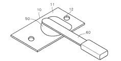
図1は、実施の形態1に係る半導体装置における金属箔としてのアルミ箔10を示す斜視図である。図1において、アルミ箔10の片側の塗布面11のみの全域に、ジョイントコンパウンドとしてのシリコーングリース50が、ヘラ60を用いて人手により均一に塗布される。また、アルミ箔10には、放熱部材としての冷却フィンを取り付けるためのネジ穴12が形成されている。このとき、アルミ箔10の厚みとしては、3〜50μm程度が望ましく、塗布されるシリコーングリース50の厚みとしては、50〜500μm程度が望ましい。また、アルミ箔10は、後述する半導体モジュール100のベース面111と、略同一形状を有している。シリコーングリース50が塗布されたアルミ箔10は、後述するように、半導体モジュールと冷却フィンとに挟持され、緩衝部材として機能する。
<
FIG. 1 is a perspective view showing an
次に、本実施の形態の背景として、図2〜3を用いて、従来の半導体装置におけるシリコーングリース50の塗布手法を説明する。
Next, as a background of the present embodiment, a method for applying the
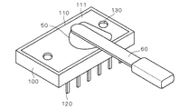
図2の斜視図において、半導体モジュール100は、図示しない半導体チップを内蔵しており、半導体モジュール100の片側には、半導体チップの発熱を放熱する放熱板としてのベース板110が、ベース面111(放熱面)を露出するように配設される。また、半導体モジュール100において、ベース板110の反対側には、信号を入出力するためのリードとしての端子120が突出するように導出されている。また、半導体モジュール100には、冷却フィンを取り付けるためのネジ穴130が形成されている。ベース板110には、シリコーングリース50が、ヘラ60を用いて人手により塗布される。
In the perspective view of FIG. 2, the
図3は、シリコーングリース50が塗布された半導体モジュール100に、冷却フィン200が取り付けられた様子を示す断面図である。ここで、図3(a)は、半導体モジュール100のベース面111及び冷却フィン200の取り付け面201の中央付近が凹んでいる場合を示し、図3(b)は、ベース面111及び取り付け面201の中央付近が凸んでいる場合を示している。
FIG. 3 is a cross-sectional view illustrating a state in which the
図3に示すように、半導体モジュール100は、半導体チップ140を、モールド樹脂150(パッケージ)により封止したものである。冷却フィン200にはネジ穴210が形成されており、ネジ穴130,210をネジ300で止めることにより、ベース面111と取り付け面201とは当接し締結されている。ここで、ベース面111の面積(第1の面積)は、取り付け面201の面積(第2の面積)よりも小さいものとする。
As shown in FIG. 3, the
図3(a)においては、ベース面111及び取り付け面201の中央付近で、シリコーングリース50が厚い層となっている。また、図3(b)においては、ベース面111及び取り付け面201の端部付近で、シリコーングリース50が厚い層となっている。
In FIG. 3A, the
しかし、上述したように、半導体モジュール100のベース板110にシリコーングリース50を直接に塗布する場合には、精度よく塗布することが困難であるので、半導体チップ140が破壊されてしまう場合がある。そこで、図1に示すようなアルミ箔10の片側の塗布面11にシリコーングリース50を塗布しておき、以下に説明するように、このアルミ箔10を用いて、半導体モジュール100と冷却フィン200とを取り付ける。
However, as described above, when the
図4は、図1に示されるようなアルミ箔10を用いて半導体モジュール100と冷却フィン200とを取り付けた、本実施の形態に係る半導体装置の構造を示す断面図である。この半導体装置は、アルミ箔10の塗布面11に塗布されたシリコーングリース50が半導体モジュール100と密接するようにして、半導体モジュール100と冷却フィン200とを取り付けたものである。即ち、図4(a),(b)はそれぞれ、図3(a),(b)において、シリコーングリース50と冷却フィン200との間にアルミ箔10を配置させ、アルミ箔10のネジ穴12をネジ300で止めたものである。
FIG. 4 is a cross-sectional view showing the structure of the semiconductor device according to the present embodiment in which the
図1に示されるようなアルミ箔10を用いて半導体モジュール100と冷却フィン200とを取り付けるときには、図5(a),(b)に示すように、製造ラインの外で予めシリコーングリース50を塗布したアルミ箔10を、製造ライン上で半導体モジュール100(のベース面)に密着させた後に、冷却フィン200のネジ止めによる取り付けを行うことにより、取り付けを容易に行うことができる。
When the
このように、本実施の形態に係る半導体装置は、アルミ箔10の片側の塗布面11のみに塗布されたシリコーングリース50が半導体モジュール100と密接するようにして、半導体モジュール100と冷却フィン200とをネジ止めにより取り付けるので、人手にて作業を行う場合の取り扱いが容易であり且つベース板110と冷却フィン200との間に隙間が形成されない。従って、放熱性を低下させることなく且つ人手により容易に製造できるという効果を有する。また、塗布されるシリコーングリース50の量を低減することができるという効果を有する。
Thus, in the semiconductor device according to the present embodiment, the
なお、上記の説明においては、ベース面111の面積(第1の面積)が取り付け面201の面積(第2の面積)よりも小さい場合について説明したが、ベース面111の面積は、取り付け面201の面積よりも大きくてもよい。この場合には、アルミ箔10としては、取り付け面201と略同一形状を有するものを用いて、シリコーングリース50が冷却フィン200と密接するようにして取り付けを行う。即ち、ベース面111と取り付け面201とのうち、より面積の小さい方の面にシリコーングリース50が密接するようにして、取り付けを行う。
In the above description, the case where the area (first area) of the
また、金属箔は、アルミ箔に限らず金属を材料とするものであればよく、例えば銀箔板等であってもよい。金属材料を用いることにより、放熱性を高くすることが可能となる。但し、冷却フィン200との接触により電池が形成されることを避けるためには、冷却フィン200と同種の金属であることが好ましい。従って、例えば、冷却フィン200がアルミニウムを材料としている場合には、金属箔として、アルミ箔を用いることにより、銀箔板等を用いる場合に比べて、腐食の進行を防止することができる。
Further, the metal foil is not limited to an aluminum foil, and any metal foil may be used, for example, a silver foil plate or the like. By using a metal material, it is possible to increase heat dissipation. However, in order to avoid the formation of a battery due to contact with the cooling
<実施の形態2>
図6は、実施の形態2に係る半導体装置における金属箔としてのアルミ箔20を示す断面図である。アルミ箔20は、実施の形態1に係る図1のアルミ箔10の主面全域に、直径0.1〜0.5mm程度の微小な貫通孔21を複数形成したものである。
<Embodiment 2>
FIG. 6 is a cross-sectional view showing an
一般に、シリコーングリース50は、熱伝導の良いセラミック粉末を媒介液で練ることにより作製される。従って、アルミ箔20に貫通孔21を形成することにより、半導体モジュール100と冷却フィン200とを取り付けるときに、媒介液と、シリコーングリース50に含まれるセラミック粉末のうちの微細な粉末とが、貫通孔21を通過して塗布面11の反対側の面にも染み出すので、密着性を高めることができる。従って、放熱性をさらに高めることができる。
In general, the
このように、本実施の形態に係る半導体装置においては、主面全域に貫通孔21を形成されたアルミ箔20を用いて取り付けが行われるので、実施の形態1の効果に加えて、放熱性をさらに高めることができるという効果を有する。
Thus, in the semiconductor device according to the present embodiment, since the attachment is performed using the
<実施の形態3>
実施の形態2に係る半導体装置においては、主面全域に貫通孔21を形成されたアルミ箔20を用いることにより、シリコーングリース50を塗布面11の反対側の面にも染み出すようにしている。しかし、図7(a)に示すように、アルミ箔20に代えて、布状もしくは網状のアルミ細線からなり可撓性を有するアルミ板30(網状金属板)を用いてもよい。図7(b)は、図7(a)の一部(点線で囲んだ領域)を拡大したものである。このアルミ板30を構成するアルミ細線31としては、直径5〜30μmであることが望ましい。アルミ板30は、アルミ箔20よりも取り扱い易く、損傷しにくいので、半導体装置をさらに容易に製造することができる。
<Embodiment 3>
In the semiconductor device according to the second embodiment, the
このように、本実施の形態に係る半導体装置においては、布状もしくは網状のアルミ細線からなり可撓性を有するアルミ板30を用いて取り付けが行われる。従って、実施の形態2の効果に加えて、半導体装置をさらに容易に製造することができるという効果を有する。
Thus, in the semiconductor device according to the present embodiment, attachment is performed using the
10,20 アルミ箔、12,130,210 ネジ穴、11 塗布面、21 貫通孔、30 アルミ板、31 アルミ細線、50 シリコーングリース、60 ヘラ、100 半導体モジュール、110 ベース板、111 ベース面、120 端子、140 半導体チップ、150 モールド樹脂、200 冷却フィン、201 取り付け面、300 ネジ。
10, 20 Aluminum foil, 12, 130, 210 Screw hole, 11 Application surface, 21 Through hole, 30 Aluminum plate, 31 Aluminum fine wire, 50 Silicone grease, 60 spatula, 100 Semiconductor module, 110 Base plate, 111 Base surface, 120 Terminal, 140 Semiconductor chip, 150 Mold resin, 200 Cooling fin, 201 Mounting surface, 300 Screw.
Claims (6)
第2の面積を有する取り付け面が形成された放熱部材を用意する工程と、
片面全域にコンパウンドが均一に塗布された緩衝部材を用意する工程と、
前記コンパウンドが、前記第1の面積を有する放熱面と前記第2の面積を有する取り付け面のうち、より面積の小さい方の面と密接するように、前記緩衝部材を前記半導体モジュールまたは前記放熱部材に密着させる工程と、
前記取り付け面に前記放熱面が対向配置され、しかも前記半導体モジュールまたは前記放熱部材に密着させた前記緩衝部材を挟持するように、前記放熱部材を前記半導体モジュールと締結する工程と
を備えることを特徴とする半導体装置の製造方法。 Preparing a semiconductor module in which a heat dissipation surface having a first area is formed;
Preparing a heat dissipating member on which a mounting surface having a second area is formed;
A step of preparing a buffer member in which the compound is uniformly applied to the entire area of one side;
The buffer member is placed on the semiconductor module or the heat radiating member so that the compound is in close contact with the smaller surface of the heat radiating surface having the first area and the mounting surface having the second area. A step of closely adhering to
And a step of fastening the heat radiating member to the semiconductor module so that the heat radiating surface is opposed to the mounting surface and the buffer member in close contact with the semiconductor module or the heat radiating member is sandwiched. A method for manufacturing a semiconductor device.
前記第1の面積より大きい第2の面積を有する取り付け面が形成された放熱部材を用意する工程と、
片面全域にコンパウンドが均一に塗布された緩衝部材を用意する工程と、
前記コンパウンドが、前記第1の面積を有する放熱面と密接するように、前記緩衝部材を前記半導体モジュールに密着させる工程と、
前記取り付け面に前記放熱面が対向配置され、しかも前記半導体モジュールに密着させた前記緩衝部材を挟持するように、前記放熱部材を前記半導体モジュールと締結する工程と
を備えることを特徴とする半導体装置の製造方法。 Preparing a semiconductor module in which a heat-radiating surface having a first area and a terminal protruding on the back surface of the heat-radiating surface are formed;
Preparing a heat dissipating member on which a mounting surface having a second area larger than the first area is formed;
A step of preparing a buffer member in which the compound is uniformly applied to the entire area of one side;
Adhering the buffer member to the semiconductor module so that the compound is in intimate contact with the heat dissipation surface having the first area;
A step of fastening the heat dissipating member to the semiconductor module so that the heat dissipating surface is opposed to the mounting surface, and the buffer member is in close contact with the semiconductor module. Manufacturing method.
Priority Applications (1)
| Application Number | Priority Date | Filing Date | Title |
|---|---|---|---|
| JP2003362916A JP4091896B2 (en) | 2003-10-23 | 2003-10-23 | Manufacturing method of semiconductor device |
Applications Claiming Priority (1)
| Application Number | Priority Date | Filing Date | Title |
|---|---|---|---|
| JP2003362916A JP4091896B2 (en) | 2003-10-23 | 2003-10-23 | Manufacturing method of semiconductor device |
Publications (2)
| Publication Number | Publication Date |
|---|---|
| JP2005129675A JP2005129675A (en) | 2005-05-19 |
| JP4091896B2 true JP4091896B2 (en) | 2008-05-28 |
Family
ID=34642380
Family Applications (1)
| Application Number | Title | Priority Date | Filing Date |
|---|---|---|---|
| JP2003362916A Expired - Fee Related JP4091896B2 (en) | 2003-10-23 | 2003-10-23 | Manufacturing method of semiconductor device |
Country Status (1)
| Country | Link |
|---|---|
| JP (1) | JP4091896B2 (en) |
Families Citing this family (5)
| Publication number | Priority date | Publication date | Assignee | Title |
|---|---|---|---|---|
| JP4711792B2 (en) * | 2005-09-26 | 2011-06-29 | 三洋電機株式会社 | Circuit equipment |
| JP4847357B2 (en) * | 2007-01-29 | 2011-12-28 | 本田技研工業株式会社 | Manufacturing method of semiconductor device |
| CN102856265A (en) * | 2012-09-28 | 2013-01-02 | 西安永电电气有限责任公司 | Bottom plate with arc-shaped bosses for IGBT (Insulated Gate Bipolar Transistor) module |
| JP5700092B2 (en) * | 2013-09-06 | 2015-04-15 | トヨタ自動車株式会社 | Semiconductor device |
| WO2015097874A1 (en) * | 2013-12-27 | 2015-07-02 | 三菱電機株式会社 | Semiconductor device |
-
2003
- 2003-10-23 JP JP2003362916A patent/JP4091896B2/en not_active Expired - Fee Related
Also Published As
| Publication number | Publication date |
|---|---|
| JP2005129675A (en) | 2005-05-19 |
Similar Documents
| Publication | Publication Date | Title |
|---|---|---|
| US10249552B2 (en) | Semiconductor package having double-sided heat dissipation structure | |
| JP4610414B2 (en) | Electronic component storage package, electronic device, and electronic device mounting structure | |
| TWI521653B (en) | Semiconductor device | |
| JPH08222671A (en) | Cooler for circuit module | |
| JP2009105366A (en) | Semiconductor device and method of manufacturing semiconductor device as well as package of semiconductor device | |
| JP4917296B2 (en) | Manufacturing method of semiconductor device | |
| JP4091896B2 (en) | Manufacturing method of semiconductor device | |
| JP3669980B2 (en) | MODULE STRUCTURE MANUFACTURING METHOD, CIRCUIT BOARD FIXING METHOD, AND CIRCUIT BOARD | |
| JP2004253531A (en) | Power semiconductor module and its fixing method | |
| JP2004336046A (en) | Application specific heat sink element | |
| JPWO2005091363A1 (en) | Heat sink substrate and manufacturing method thereof | |
| JP2007012718A (en) | Electronic component housing package and electronic device | |
| US10856403B2 (en) | Power electronics module and a method of producing a power electronics module | |
| JPH11312770A (en) | Radiation fin for thin ic | |
| JP4030845B2 (en) | Mounting structure of IC having QFP structure, mounting method thereof, and assembly jig used for mounting | |
| JPH09226280A (en) | Card module | |
| JP4514598B2 (en) | Electronic component storage package and electronic device | |
| JP3669981B2 (en) | Method for manufacturing module structure | |
| JP2008243877A (en) | Power module and its manufacturing method | |
| JP2004296726A (en) | Heat dissipating member, package for containing semiconductor element, and semiconductor device | |
| JPS627145A (en) | Power semiconductor device | |
| JP2003068954A (en) | Package for housing semiconductor element | |
| JP2004247514A (en) | Semiconductor element housing package, and semiconductor device | |
| JP2019067804A (en) | Ceramic circuit board | |
| JP2004221328A (en) | Semiconductor element housing package and semiconductor device |
Legal Events
| Date | Code | Title | Description |
|---|---|---|---|
| A621 | Written request for application examination |
Free format text: JAPANESE INTERMEDIATE CODE: A621 Effective date: 20051226 |
|
| A977 | Report on retrieval |
Free format text: JAPANESE INTERMEDIATE CODE: A971007 Effective date: 20070903 |
|
| A131 | Notification of reasons for refusal |
Free format text: JAPANESE INTERMEDIATE CODE: A131 Effective date: 20070911 |
|
| A521 | Written amendment |
Free format text: JAPANESE INTERMEDIATE CODE: A523 Effective date: 20071003 |
|
| RD04 | Notification of resignation of power of attorney |
Free format text: JAPANESE INTERMEDIATE CODE: A7424 Effective date: 20071003 |
|
| A131 | Notification of reasons for refusal |
Free format text: JAPANESE INTERMEDIATE CODE: A131 Effective date: 20071204 |
|
| A521 | Written amendment |
Free format text: JAPANESE INTERMEDIATE CODE: A523 Effective date: 20080122 |
|
| TRDD | Decision of grant or rejection written | ||
| A01 | Written decision to grant a patent or to grant a registration (utility model) |
Free format text: JAPANESE INTERMEDIATE CODE: A01 Effective date: 20080226 |
|
| A61 | First payment of annual fees (during grant procedure) |
Free format text: JAPANESE INTERMEDIATE CODE: A61 Effective date: 20080229 |
|
| R150 | Certificate of patent or registration of utility model |
Ref document number: 4091896 Country of ref document: JP Free format text: JAPANESE INTERMEDIATE CODE: R150 Free format text: JAPANESE INTERMEDIATE CODE: R150 |
|
| FPAY | Renewal fee payment (event date is renewal date of database) |
Free format text: PAYMENT UNTIL: 20110307 Year of fee payment: 3 |
|
| FPAY | Renewal fee payment (event date is renewal date of database) |
Free format text: PAYMENT UNTIL: 20110307 Year of fee payment: 3 |
|
| FPAY | Renewal fee payment (event date is renewal date of database) |
Free format text: PAYMENT UNTIL: 20120307 Year of fee payment: 4 |
|
| FPAY | Renewal fee payment (event date is renewal date of database) |
Free format text: PAYMENT UNTIL: 20130307 Year of fee payment: 5 |
|
| FPAY | Renewal fee payment (event date is renewal date of database) |
Free format text: PAYMENT UNTIL: 20130307 Year of fee payment: 5 |
|
| FPAY | Renewal fee payment (event date is renewal date of database) |
Free format text: PAYMENT UNTIL: 20140307 Year of fee payment: 6 |
|
| R250 | Receipt of annual fees |
Free format text: JAPANESE INTERMEDIATE CODE: R250 |
|
| R250 | Receipt of annual fees |
Free format text: JAPANESE INTERMEDIATE CODE: R250 |
|
| R250 | Receipt of annual fees |
Free format text: JAPANESE INTERMEDIATE CODE: R250 |
|
| R250 | Receipt of annual fees |
Free format text: JAPANESE INTERMEDIATE CODE: R250 |
|
| R250 | Receipt of annual fees |
Free format text: JAPANESE INTERMEDIATE CODE: R250 |
|
| LAPS | Cancellation because of no payment of annual fees |