JP4087224B2 - Information recording / reproducing apparatus and information reproducing method - Google Patents
Information recording / reproducing apparatus and information reproducing method Download PDFInfo
- Publication number
- JP4087224B2 JP4087224B2 JP2002325832A JP2002325832A JP4087224B2 JP 4087224 B2 JP4087224 B2 JP 4087224B2 JP 2002325832 A JP2002325832 A JP 2002325832A JP 2002325832 A JP2002325832 A JP 2002325832A JP 4087224 B2 JP4087224 B2 JP 4087224B2
- Authority
- JP
- Japan
- Prior art keywords
- synchronization
- signal
- address
- recording
- timing signal
- Prior art date
- Legal status (The legal status is an assumption and is not a legal conclusion. Google has not performed a legal analysis and makes no representation as to the accuracy of the status listed.)
- Expired - Fee Related
Links
Images


Classifications
-
- G—PHYSICS
- G11—INFORMATION STORAGE
- G11B—INFORMATION STORAGE BASED ON RELATIVE MOVEMENT BETWEEN RECORD CARRIER AND TRANSDUCER
- G11B20/00—Signal processing not specific to the method of recording or reproducing; Circuits therefor
- G11B20/10—Digital recording or reproducing
- G11B20/18—Error detection or correction; Testing, e.g. of drop-outs
- G11B20/1833—Error detection or correction; Testing, e.g. of drop-outs by adding special lists or symbols to the coded information
-
- G—PHYSICS
- G11—INFORMATION STORAGE
- G11B—INFORMATION STORAGE BASED ON RELATIVE MOVEMENT BETWEEN RECORD CARRIER AND TRANSDUCER
- G11B27/00—Editing; Indexing; Addressing; Timing or synchronising; Monitoring; Measuring tape travel
- G11B27/10—Indexing; Addressing; Timing or synchronising; Measuring tape travel
- G11B27/19—Indexing; Addressing; Timing or synchronising; Measuring tape travel by using information detectable on the record carrier
- G11B27/28—Indexing; Addressing; Timing or synchronising; Measuring tape travel by using information detectable on the record carrier by using information signals recorded by the same method as the main recording
- G11B27/30—Indexing; Addressing; Timing or synchronising; Measuring tape travel by using information detectable on the record carrier by using information signals recorded by the same method as the main recording on the same track as the main recording
- G11B27/3027—Indexing; Addressing; Timing or synchronising; Measuring tape travel by using information detectable on the record carrier by using information signals recorded by the same method as the main recording on the same track as the main recording used signal is digitally coded
-
- G—PHYSICS
- G11—INFORMATION STORAGE
- G11B—INFORMATION STORAGE BASED ON RELATIVE MOVEMENT BETWEEN RECORD CARRIER AND TRANSDUCER
- G11B27/00—Editing; Indexing; Addressing; Timing or synchronising; Monitoring; Measuring tape travel
- G11B27/36—Monitoring, i.e. supervising the progress of recording or reproducing
Landscapes
- Engineering & Computer Science (AREA)
- Signal Processing (AREA)
- Signal Processing For Digital Recording And Reproducing (AREA)
- Optical Recording Or Reproduction (AREA)
Description
【0001】
【発明の属する技術分野】
本発明は、情報記録再生装置及び情報再生方法に関する。
【0002】
【従来の技術】
近年、CD−RW、DVD−RWの如き情報データの書込が可能な記録ディスク、並びに、かかる記録ディスクに情報データを書き込むディスクレコーダが普及してきた。このような記録ディスクには、ディスク上の位置を表すディスクアドレス及び同期信号が予め記録されている。ディスクレコーダは、その記録動作を開始するにあたり、記録ディスクから読み取られた読取信号中から上記同期信号を検出し、この同期信号に基づいて上記ディスクアドレス復調の為のタイミング信号を発生させるようにしている。よって、隣接トラックからのクロストーク、又はディスク表面に付着した埃、傷、指紋等の外乱の影響により読取信号が一時的に乱れると、同期信号に対するタイミング信号の位相同期状態が解除されてしまう。すると、同期信号が正常な状態に復帰した際に、再びこの同期信号に位相同期させる為に再同期処理を実行しなければならず、この間、ディスクレコーダは記録動作を中断、又は記録動作を開始させることができなくなるという問題があった。
【0003】
【発明が解決しようとする課題】
本発明は、外乱等の影響を受けても迅速に情報データの記録を完了させることができる情報記録再生装置及び情報再生方法を提供することを目的とする。
【0004】
【課題を解決するための手段】
請求項1に記載の情報記録再生装置は、同期信号及び記録位置を表すアドレスが予め変調して記録されている記録媒体に対して情報データの記録又は再生を行う情報記録再生装置であって、前記記録媒体から記録情報の読み取りを行って読取信号を得る読取手段と、復調タイミング信号に応じて前記読取信号から前記同期信号及び前記アドレスを示すアドレスデータを夫々復調する復調手段と、前記復調タイミング信号を発生すると共に、同期指令に応じて前記同期信号に同期させるべき同期処理を前記復調タイミング信号に施すタイミング信号生成手段と、前記アドレスデータに対して誤り訂正処理を施して訂正アドレスデータを得る誤り訂正手段と、前記訂正アドレスデータが正しいアドレスであるか否かを判定するアドレス判定手段と、前記同期信号の周期が所定周期と一致しない場合に前記同期指令を発令すべき同期制御を実行する同期制御手段と、を有し、前記同期制御手段は、前記訂正アドレスデータが正しいアドレスであると判定された場合にはその後、前記訂正アドレスデータが不正なアドレスであると判定されるまで前記同期制御の実行を待機させる。
【0005】
又、請求項5に記載の情報記録再生装置は、同期信号及び記録位置を表すアドレスが予め変調して記録されている記録媒体に対して情報データの記録又は再生を行う情報記録再生装置であって、前記記録媒体から記録情報の読み取りを行って読取信号を得る読取手段と、復調タイミング信号に応じて前記読取信号から前記同期信号を復調する復調手段と、前記復調タイミング信号を発生すると共に、同期指令に応じて前記同期信号に同期させるべき同期処理を前記復調タイミング信号に施すタイミング信号生成手段と、前記同期信号の周期が所定周期と一致しない場合に前記同期指令を発令すべき同期制御を実行する同期制御手段と、を有し、前記同期制御手段は、前記情報データを前記記録媒体に記録する記録動作中には前記同期制御の実行を待機させる。
【0006】
又、請求項7に記載の情報再生装置は、同期信号及び記録位置を表すアドレスが予め変調して記録されている記録媒体に対して情報データの再生を行う情報再生装置であって、前記記録媒体から記録情報の読み取りを行って読取信号を得る読取手段と、復調タイミング信号に応じて前記読取信号から前記同期信号及び前記アドレスを示すアドレスデータを夫々復調する復調手段と、前記復調タイミング信号を発生すると共に、同期指令に応じて前記同期信号に同期させるべき同期処理を前記復調タイミング信号に施すタイミング信号生成手段と、前記アドレスデータに対して誤り訂正処理を施して訂正アドレスデータを得る誤り訂正手段と、前記訂正アドレスデータが正しいアドレスであるか否かを判定するアドレス判定手段と、前記同期信号の周期が所定周期と一致しない場合に前記同期指令を発令すべき同期制御を実行する同期制御手段と、を有し、前記同期制御手段は、前記訂正アドレスデータが正しいアドレスであると判定された場合にはその後、前記訂正アドレスデータが不正なアドレスであると判定されるまで前記同期制御の実行を待機させる。
【0007】
又、請求項8に記載の情報再生方法は、同期信号及び記録位置を表すアドレスが予め変調して記録されている記録媒体に対して情報データを記録又は再生する際に前記記録媒体から前記同期信号及び前記アドレスの再生を行う情報再生方法であって、前記記録媒体から記録情報の読み取りを行って読取信号を得る読取行程と、復調タイミング信号に応じて前記読取信号から前記同期信号及び前記アドレスを示すアドレスデータを夫々復調する復調行程と、前記復調タイミング信号を発生すると共に、同期指令に応じて前記同期信号に同期させるべき同期処理を前記復調タイミング信号に施すタイミング信号生成行程と、前記アドレスデータに対して誤り訂正処理を施して訂正アドレスデータを得る誤り訂正行程と、前記訂正アドレスデータが正しいアドレスであるか否かを判定するアドレス判定行程と、前記同期信号の周期が所定周期と一致しない場合に前記同期指令を発令すべき同期制御を実行する同期制御行程と、を有し、前記同期制御行程は、前記訂正アドレスデータが正しいアドレスであると判定された場合にはその後、前記訂正アドレスデータが不正なアドレスであると判定されるまで前記同期制御の実行を待機する。
【0008】
又、請求項12に記載の情報再生方法は、同期信号及び記録位置を表すアドレスが予め変調して記録されている記録媒体に対して情報データを記録又は再生する際に前記記録媒体から前記同期信号及び前記アドレスの再生を行う情報再生方法であって、前記記録媒体から記録情報の読み取りを行って読取信号を得る読取行程と、復調タイミング信号に応じて前記読取信号から前記同期信号を復調する復調行程と、前記復調タイミング信号を発生すると共に、同期指令に応じて前記同期信号に同期させるべき同期処理を前記復調タイミング信号に施すタイミング信号生成行程と、前記同期信号の周期が所定周期と一致しない場合に前記同期指令を発令すべき同期制御を実行する同期制御行程と、を有し、前記同期制御行程は、前記情報データを前記記録媒体に記録する記録動作中には前記同期制御の実行を待機する。
又、請求項14に記載の情報記録再生装置は、同期信号及び記録位置を表すアドレスが予め変調して記録されている記録媒体に対して情報データの記録又は再生を行う情報記録再生装置であって、前記記録媒体から記録情報の読み取りを行って読取信号を得る読取手段と、復調タイミング信号に応じて前記読取信号から前記同期信号及び前記アドレスを示すアドレスデータを夫々復調する復調手段と、前記復調タイミング信号を発生すると共に、同期指令に応じて前記同期信号に同期させるべき同期処理を前記復調タイミング信号に施すタイミング信号生成手段と、前記アドレスデータに対して誤り訂正処理を施して訂正アドレスデータを得る誤り訂正手段と、前記訂正アドレスデータが正しいアドレスであるか否かを判定するアドレス判定手段と、前記同期指令を発令すべき同期制御を実行する同期制御手段と、を有し、前記タイミング信号生成手段は、前記同期信号のタイミングにて所定の初期値を取り込みこの初期値からカウント動作を行う第1カウンタと、前記第1カウンタのカウント値が所定値と一致したときにパルス信号を発生しこれを仮同期復調タイミング信号として出力する第1デコーダと、前記同期指令に応じて前記同期信号のタイミングにて前記第1カウンタのカウント値を取り込みこのカウント値からカウント動作を行う第2カウンタと、前記第2カウンタのカウント値が所定の第1又は第2カウント値と一致したときにパルス信号を発生し、前記第1カウント値と一致したときに発生した前記パルス信号を前記復調タイミング信号として出力する一方、前記第2カウント値と一致したときに発生した前記パルス信号を同期復調タイミング信号として出力する手段と、からなり、前記同期制御手段は、前記同期信号及び前記仮同期復調タイミング信号同士のタイミングが一致しており、且つ前記同期信号及び前記同期復調タイミング信号同士のタイミングが不一致となっている場合に前記同期制御を実行する一方、前記訂正アドレスデータが正しいアドレスであると判定された場合にはその後、前記訂正アドレスデータが不正なアドレスであると判定されるまで前記同期制御の実行を待機させる。
又、請求項16に記載の情報再生方法は、同期信号及び記録位置を表すアドレスが予め変調して記録されている記録媒体に対して情報データを記録又は再生する際に前記記録媒体から前記同期信号及び前記アドレスの再生を行う情報再生方法であって、前記記録媒体から記録情報の読み取りを行って読取信号を得る読取行程と、復調タイミング信号に応じて前記読取信号から前記同期信号及び前記アドレスを示すアドレスデータを夫々復調する復調行程と、前記復調タイミング信号を発生すると共に、同期指令に応じて前記同期信号に同期させるべき同期処理を前記復調タイミング信号に施すタイミング信号生成行程と、前記アドレスデータに対して誤り訂正処理を施して訂正アドレスデータを得る誤り訂正行程と、前記訂正アドレスデータが正しいアドレスであるか否かを判定するアドレス判定行程と、前記同期指令を発令すべき同期制御を実行する同期制御行程と、を有し、前記タイミング信号生成行程は、前記同期信号のタイミングにて所定の初期値を取り込みこの初期値からカウント動作を行う第1計数行程と、前記第1計数行程でのカウント値が所定値と一致したときにパルス信号を発生しこれを仮同期復調タイミング信号として出力する第1デコード行程と、前記同期指令に応じて前記同期信号のタイミングにて前記第1計数行程でのカウント値を取り込みこのカウント値からカウント動作を行う第2計数行程と、前記第2計数行程でのカウント値が所定の第1又は第2カウント値と一致したときにパルス信 号を発生し、前記第1カウント値と一致したときに発生した前記パルス信号を前記復調タイミング信号として出力する一方、前記第2カウント値と一致したときに発生した前記パルス信号を同期復調タイミング信号として出力する行程と、からなり、前記同期制御行程は、前記同期信号及び前記仮同期復調タイミング信号同士のタイミングが一致しており、且つ前記同期信号及び前記同期復調タイミング信号同士のタイミングが不一致となっている場合に前記同期制御を実行する一方、前記訂正アドレスデータが正しいアドレスであると判定された場合にはその後、前記訂正アドレスデータが不正なアドレスであると判定されるまで前記同期制御の実行を待機させる。
【0009】
【発明の実施の形態】
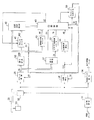
図1は、記録ディスク30に対して情報データの記録又は再生を行う情報記録再生装置の構成を示す図である。
図1において、記録変調回路31は、記録ディスク30に記録すべき情報データに対して所定の記録変調方式に従った変調処理を施して得られた変調記録信号を記録再生ヘッド32に供給する。記録ディスク30には、ディスク上の位置を表すディスクアドレス及び記録・再生制御時の同期タイミングを担う同期信号が予め記録されている。尚、これらディスクアドレス及び同期信号には、上記の如き記録変調方式に基づく変調処理が施されている。記録再生ヘッド32は、スピンドルモータ33によって回転する記録ディスク30の記録面に記録ビーム光又は読取ビーム光を照射する。すなわち、記録再生ヘッド32は、記録ディスク30に情報データを記録する際には、上記変調記録信号に応じた記録ビーム光を記録ディスク30の記録面に照射する。一方、記録ディスク30から情報データを再生する際には、記録再生ヘッド32は、記録ディスク30の記録面に読取ビーム光を照射する。この際、記録再生ヘッド32は、記録ディスク30の記録面からの反射光を光電変換して読取信号を生成し、これを情報データ再生回路34、アドレス復調回路35及び同期検出回路36の各々に供給する。情報データ再生回路34は、かかる読取信号に対して所定の復調処理を行うことにより、記録ディスク30に記録されている情報データを復元し、これを再生情報データとして出力する。
【0010】
アドレス復調回路35は、タイミング信号生成回路50(後述する)から供給されたアドレス復調タイミング信号AXに応じて上記読取信号に対して復調処理を施す。かかる復調処理によりアドレス復調回路35は、ディスクアドレスを復調し、このディスクアドレスを表すアドレスデータADを誤り検出回路37及び誤り訂正回路38の各々に供給する。
【0011】
誤り検出回路37は、上記アドレスデータADに対して誤り検出処理を施す。かかる誤り検出処理により誤り検出回路37は、1符号ブロック分のアドレスデータAD毎に、このアドレスデータAD中に誤りが存在する場合には論理レベル0、存在しない場合には論理レベル1の誤りゼロ信号E0を生成し、これを同期制御回路40に供給する。更に、誤り検出回路37は、1符号ブロック分のアドレスデータAD毎に、このアドレスデータADが誤り訂正可能である場合には論理レベル0、誤り訂正が不可能である場合には論理レベル1の訂正不可信号ERを生成し、これを訂正不可連続数カウンタ39に供給する。
【0012】
訂正不可連続数カウンタ39は、訂正不可信号ERが連続して論理レベル1となる回数を計数し、その回数を示す訂正不可連続回数信号FNを同期制御回路40に供給する。すなわち、訂正不可連続数カウンタ39は、アドレスデータADが符号ブロック単位で連続して誤り訂正不可能となる回数を示す訂正不可連続回数信号FNを同期制御回路40に供給するのである。尚、訂正不可連続回数カウンタ39は、訂正不可信号ERが論理レベル0となる度に、その計数値を0にリセットする。
【0013】
誤り訂正回路38は、上記アドレスデータADに対して誤り訂正処理を施し、この誤り訂正処理によって誤り訂正の為されたアドレスデータを訂正アドレスデータADRとしてアドレスカウンタ41、記録再生制御回路42及び連続変化数カウンタ43の各々に供給する。
図2は、アドレスカウンタ41の内部構成を示す図である。
【0014】
図2において、加算器410は、訂正アドレスデータADRに「1」を加算した値をカウンタ411のロードデータ端子DTに供給する。アンドゲート412は、同期制御回路40から論理レベル1のアドレス正常状態信号G2が供給され、かつタイミング信号生成回路50から論理レベル1のデータ確定信号FXが供給された場合に限り論理レベル1のデータロード信号をカウンタ411のデータロード制御端子LDに供給する。カウンタ411は、所定期間経過毎に1ずつカウントアップするカウントアップ動作を行い、現時点でのカウント値を生成アドレスデータADCとして出力する。尚、カウンタ411は、論理レベル1のデータロード信号が供給された場合には、上記訂正アドレスデータADRに1を加算した値をカウント初期値として取り込み、このカウント初期値から引き続き上述した如きカウントアップ動作を行う。尚、カウンタ411は、そのカウント値が所定の最大値に達したらカウント値を0にリセットして、上述した如きカウントアップ動作を継続する。
【0015】
かかる構成により、アドレスカウンタ41は、上述した如きカウントアップ動作にて得られた現時点でのカウント値を生成アドレスデータADCとして記録再生制御回路42に供給する。この際、論理レベル1のアドレス正常状態信号G2が供給されている間に論理レベル1のデータ確定信号FXが供給された場合には、アドレスデータADRに1を加算した値をカウント初期値として取り込み、このカウント初期値から引き続きカウントアップ動作を行う。
【0016】
連続変化数カウンタ43は、上記訂正アドレスデータADRが1ずつ連続して増加又は減少する回数を計数し、その回数を示すアドレス連続変化数信号ANを同期制御回路40に供給する。尚、連続変化数カウンタ43は、上記訂正アドレスデータADRが所定期間経過後に2以上増加(又は減少)した場合、つまり訂正アドレスデータADRにおける1ずつの連続増加(又は減少)が途絶えた場合には、そのカウント回数を0にリセットする。
【0017】
記録再生制御回路42は、ユーザからの各種操作に応じてこの情報記録再生装置の各種記録動作及び再生動作を実施させるべく、記録再生ヘッド32、スピンドルモータ33、及び記録再生ヘッド32をディスク半径方向に移送せしめるスライダ機構(図示せぬ)を制御する。尚、記録動作時には、記録再生制御回路42は、記録ディスク30上の所望のディスク位置から記録を開始させるべく、上記生成アドレスデータADC又は訂正アドレスデータADRに基づきそのディスク位置の検索を行う。
【0018】
同期検出回路36は、タイミング信号生成回路50(後述する)から供給された同期復調タイミング信号SXに応じて上記読取信号に対して復調処理を施すことにより同期信号を復調する。同期検出回路36は、この復調処理によって復調された同期信号の検出タイミングにて論理レベル0から論理レベル1に推移する同期パルスを含む同期検出信号SYCを同期制御回路40、同期異常検出回路44及びタイミング信号生成回路50に夫々供給する。
【0019】
同期異常検出回路44は、同期検出信号SYCによる同期パルスの周期が所定周期Tである場合には「同期異常なし」を示す論理レベル0の同期異常検出信号ABを同期制御回路40に供給する。一方、同期検出信号SYCによる同期パルスの周期が所定周期Tではない場合には、同期異常検出回路44は「同期異常有り」を示す論理レベル1の同期異常検出信号ABを同期制御回路40に供給する。すなわち、同期異常検出回路44は、記録ディスク30から正しく同期信号を読み取ることができた場合には論理レベル0、正しく同期信号を読み取ることができなかった場合には論理レベル1の同期異常検出信号ABを同期制御回路40に供給するのである。
【0020】
タイミング信号生成回路50は、同期検出信号SYC、及び同期制御回路40から供給された同期指令信号G1に基づき、前述した如きアドレス復調タイミング信号AX及び同期復調タイミング信号SX、並びに仮同期読取タイミング信号SSXを生成する。そして、タイミング信号生成回路50は、アドレス復調タイミング信号AX及び同期復調タイミング信号SXを夫々、アドレス復調回路35及び同期検出回路36に供給すると共に、同期復調タイミング信号SX及び仮同期読取タイミング信号SSXを同期制御回路40に供給する。更に、タイミング信号生成回路50は、同期検出信号SYC及び同期指令信号G1に基づき、前述した如きデータ確定信号FXを生成し、これをアドレスカウンタ41に供給する。
【0021】
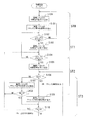
図3は、タイミング信号生成回路50の内部構成の一例を示す図である。
図3において、カウンタ501は、同期検出回路36から論理レベル1の同期検出信号SYCが供給される度に初期値を取り込み、この初期値を所定期間経過毎に1ずつカウントアップして得られたカウント値をデコーダ500及び加算器502に供給する。尚、カウンタ501は、そのカウント値が所定の最大値に達したらカウント値を0にリセットして上記カウントアップ動作を引き続き実行する。デコーダ500は、カウンタ501のカウント値が所定のカウント値と一致した場合に論理レベル0から論理レベル1に推移するパルス信号を生成し、これを仮同期読取タイミング信号SSXとして出力する。加算器502は、カウンタ501のカウント値に「1」を加算した値をカウンタ503のロードデータ端子DTに供給する。アンドゲート504は、同期制御回路40から論理レベル1の同期指令信号G1が供給され、かつ同期検出信号SYCが論理レベル1である場合に限り論理レベル1のデータロード信号をカウンタ503のデータロード制御端子LDに供給する。カウンタ503は、所定期間経過毎に1ずつカウントアップするカウントアップ動作を行い、現時点でのカウント値をデコーダ505に供給する。尚、カウンタ503は、論理レベル1のデータロード信号が供給された場合には、カウンタ501のカウント値に1を加算した値をカウント初期値として取り込み、このカウント初期値から引き続きカウントアップ動作を行う。又、カウンタ503は、そのカウント値が所定の最大値に達したらカウント値を0にリセットして、上記カウントアップ動作を引き続き実行する。デコーダ505は、カウンタ503のカウント値が所定の第1カウント値と一致した場合に論理レベル0から論理レベル1に推移するパルス信号を生成しこれをアドレス復調タイミング信号AXとして出力する。又、デコーダ505は、カウンタ503のカウント値が所定の第2カウント値と一致した場合に論理レベル0から論理レベル1に推移するパルス信号を生成しこれを同期復調タイミング信号SXとして出力する。又、デコーダ505は、カウンタ503のカウント値が所定の第3カウント値と一致した場合に、誤り検出回路37及び誤り訂正回路38において1符号ブロックに対する処理が終了したことを表す論理レベル1のデータ確定信号FXを生成する。
【0022】
同期制御回路40は、図4に示す如き同期制御ルーチンに従った手順にて、記録ディスク30から再生されたディスクアドレス及び同期信号の状態を識別し、その識別結果に応じてアドレスカウンタ41及びタイミング信号生成回路50を制御する。図4において、先ず、同期制御回路40は、論理レベル1の同期指令信号G1をタイミング生成回路50に供給する(ステップS40)。ステップS40の実行により、タイミング生成回路50のカウンタ503は、論理レベル1の同期検出信号SYCが供給される度に所定のカウンタ初期値を取り込み、カウントアップ動作を行う。これにより、デコーダ505からは、同期検出信号SYCに同期したタイミングにて、前述した如きデータ確定信号FX、アドレス復調タイミング信号AX及び同期復調タイミング信号SXが出力される。上記ステップS40の実行後、同期制御回路40は、正常なアドレスが取得されていないことを表す論理レベル0のアドレス正常状態信号G2をアドレスカウンタ41に供給する(ステップS41)。ステップS41の実行により、カウンタ41は自走する。次に、同期制御回路40は、同期異常検出信号ABが同期異常を表す論理レベル1であるか否かを判定する(ステップS42)。かかるステップS42において同期異常検出信号ABが論理レベル1である、つまり、記録ディスク30から正しく同期信号を読み取ることが出来なかったと判定されている間は、同期制御回路40は、上記ステップS40に戻って前述した如き動作を繰り返し実行する。
【0023】
一方、ステップS42において上記同期異常検出信号ABが論理レベル1ではない、つまり、記録ディスク30から正しく同期信号を読み取ることができたと判定された場合には、同期制御回路40は、論理レベル0の同期指令信号G1をタイミング生成回路50に供給する(ステップS43)。ステップS43の実行により、タイミング生成回路50のカウンタ503は自走する。次に、同期制御回路40は、誤りゼロ信号E0が誤り無し状態を表す論理レベル1であるか否かの判定を行う(ステップS44)。ステップS44において、誤りゼロ信号E0が論理レベル1ではない、つまり、アドレスデータAD中に誤りが存在すると判定された場合、同期制御回路40は、正常なアドレスが取得されていないことを表す論理レベル0のアドレス正常状態信号G2をアドレスカウンタ41に供給する(ステップS45)。ステップS45の実行により、タイミング生成回路50のカウンタ41は自走する。次に、同期制御回路40は、アドレス連続変化数信号ANが所定数Pよりも大なるアドレスの連続変化数を示しているか否かの判定を行う(ステップS46)。ステップS46においてアドレス連続変化数信号ANが所定数Pよりも大ではないと判定されると、同期制御回路40は、上記ステップS42に戻って前述した如き動作を繰り返し実行する。
【0024】
一方、上記ステップS44において誤りゼロ信号E0が論理レベル1であると判定されると、同期制御回路40は、正常なアドレスが取得されたことを表す論理レベル1のアドレス正常状態信号G2をアドレスカウンタ41に供給する(ステップS47)。ステップS47の実行により、アドレスカウンタ41は、タイミング生成回路50から論理レベル1のデータ確定信号FXが供給される度に、訂正アドレスデータADRに1を加算した値をカウンタ初期値として取り込み、その値から引き続きカウントアップ動作を行う。つまり、アドレスカウンタ41は、記録ディスク30から再生された正常な訂正アドレスデータADRに基づいて、生成アドレスデータADCを生成する。一方、上記ステップS46にてアドレス連続変化数信号ANが所定数Pよりも大であると判定されると、誤りゼロ信号E0が論理レベル0であり且つアドレス連続変化数信号ANが所定数Pよりも大であるので、アドレスカウンタ41はカウントアップ動作を行う。次に、同期制御回路40は、訂正不可連続回数信号FNが所定回数Qよりも大なる回数を示しているか否かを判定する(ステップS48)。かかるステップS48において、訂正不可連続回数信号FNが所定回数Qよりも大ではないと判定されると、同期制御回路40は、上記ステップS44の実行に戻って正常なアドレスが取得されたか否かの判定を行う。この間、ステップS48において訂正不可連続回数信号FNが所定回数Qよりも大であると判定されると、同期制御回路40は、上記ステップS42の実行に戻って前述した如き動作を繰り返し実行する。
【0025】
図5は、図4に示す同期制御ルーチンに従って同期制御回路40が同期制御処理を実行した際におけるアドレスカウンタ41及びタイミング信号生成回路50各々の設定状態の推移を示す図である。
先ず、記録ディスク30から正しく同期信号を読み取ることができないと判定(ステップS42)されている間は、論理レベル1の同期指令信号G1及び論理レベル0のアドレス正常状態信号G2が供給されるので、図5に示す如き非同期状態ST0を維持する。非同期状態ST0では、タイミング信号生成回路50内のカウンタ503は再同期処理を行う。すなわち、再生状態が不安定であっても、その時の同期検出信号に応じてデータ確定信号FX、アドレス復調タイミング信号AX及び同期復調タイミング信号SXの如き各種信号を生成する。また、アドレスカウンタは自走する。
【0026】
一方、同期信号を正しく読み取ることが出来たと判定(ステップS42)されると、図5に示す如き同期状態ST1に推移する。同期状態ST1では、論理レベル0の同期指令信号G1がタイミング信号生成回路50に供給される(ステップS43)。これにより、カウンタが自走すると共にタイミング信号生成回路50は、同期検出信号SYCに位相同期したデータ確定信号FX、アドレス復調タイミング信号AX及び同期復調タイミング信号SXの生成を開始する。この間、記録ディスク30から再生された訂正アドレスデータADRが所定数Pよりも多く連続して変化していないと判定(ステップS46)され、かつ同期信号を正しく読み取ることが出来なかったと判定(ステップS42)されると、非同期状態ST0に推移する。これにより、論理レベル1の同期指令信号G1が送出されて再同期処理が実行される。一方、訂正アドレスデータADRに誤りが存在しないと判定(ステップS44)された場合、つまり、訂正アドレスデータADRが正しいアドレスであると判定された場合にはアドレス正常状態ST2に推移する。
【0027】
アドレス正常状態ST2では、論理レベル1のアドレス正常状態信号G2がアドレスカウンタ41に供給される(ステップS47)。これにより、アドレスカウンタ41は、訂正アドレスデータADRを取り込み、そのアドレスデータ値を1ずつ増加(又は減少)して行くことにより、生成アドレスデータADCを生成して記録再生制御回路42に供給する。訂正アドレスデータADRに誤りがある(E0=「1」)と判定され、且つ訂正アドレスデータADRが所定数Pよりも多く連続変化していると判定された場合、論理レベル0のアドレス正常状態信号G2が供給され、以前に取得したアドレスデータ値を1ずつ増加(又は減少)させて行く。この間、記録ディスク30から読み取られて復調されたアドレスデータADが所定回数Qよりも多く連続して訂正不能になったと判定(ステップS48)されない限り、アドレス正常状態ST2を維持する。一方、アドレスデータADが所定回数Qよりも多く連続して訂正不能になったと判定された場合、つまり訂正アドレスデータADRが不正なアドレスであると判定された場合には、同期状態ST1に推移する。すなわち、訂正アドレスデータADRが正しいアドレスではないと判定された場合には、何等かの外乱の影響により同期がはずれた可能性有りと判断して同期状態ST1に戻って同期状態を判定する。その結果、同期がはずれたと判断した場合には論理レベル1の同期指令信号を送出することで再同期処理(同期検出信号SYCに同期したタイミングでカウンタ503に対する初期値のロードを行う)を実行するのである。
【0028】
換言すると、一旦、訂正アドレスデータADRが正しいアドレスであると判定されると、例え記録ディスク30から読み取られた同期信号が一時的に乱れても、訂正アドレスデータADRが不正なアドレスであると判定されるまで再同期処理の実行が待機されるのである。
従って、同期制御回路40による同期制御処理によれば、隣接トラックからのクロストーク又は記録ディスクの表面の傷等の外乱によって同期信号が一時的に乱れた程度では再同期処理は実施されないので、記録動作を中断させることなく迅速に情報データの記録を完了させることが可能になる。
【0029】
又、上記実施例においては、アドレスデータADの誤り状態に応じて、同期状態ST1からST2(又はST1からST2)への推移が為されるが、記録ディスク30への記録開始及び記録終了をもって同期状態ST1からST2(又はST1からST2)への推移を実施するようにしても良い。
図6は、かかる点に鑑みて為された同期制御ルーチンの他の一例を示す図である。
【0030】
図6において、同期制御回路40は、先ず、同期制御回路40は、論理レベル1の同期指令信号G1をタイミング生成回路50に供給する(ステップS60)。ステップS60の実行により、タイミング生成回路50のカウンタ503は、論理レベル1の同期検出信号SYCが供給される度に所定のカウンタ初期値を取り込み、カウントアップ動作を行う。これにより、デコーダ505からは、同期検出信号SYCに同期したタイミングにて、前述した如きデータ確定信号FX、アドレス復調タイミング信号AX及び同期復調タイミング信号SXが出力される。上記ステップS60の実行後、同期制御回路40は、同期異常検出信号ABが同期異常を表す論理レベル1であるか否かを判定する(ステップS61)。かかるステップS61において同期異常検出信号ABが論理レベル1である、つまり、記録ディスク30から正しく同期信号を読み取ることが出来なかったと判定されている間は、同期制御回路40は、ステップS60に戻って前述した如き動作を繰り返し実行する。
【0031】
一方、ステップS61において上記同期異常検出信号ABが論理レベル1ではない、つまり、記録ディスク30から正しく同期信号を読み取ることができたと判定された場合には、同期制御回路40は、論理レベル0の同期指令信号G1をタイミング生成回路50に供給する(ステップS62)。ステップS62の実行により、タイミング生成回路50のカウンタ503は自走する。ステップS2の実行後、次に、同期制御回路40は、記録ディスク30に対して情報データの記録を開始する旨を知らせる記録開始信号が記録再生制御回路42から供給されたか否かの判定を行う(ステップS63)。かかるステップS63において記録開始信号が供給されていないと判定された場合、同期制御回路40は、上記ステップS61の実行に戻って前述した如き動作を繰り返し実行する。一方、ステップS63において記録開始信号が供給されたと判定された場合には、同期制御回路40は、次に、記録ディスク30に対する情報データの記録動作を終了する旨を知らせる記録終了信号が記録再生制御回路42から供給されたか否かの判定を、記録終了信号が供給されるまで繰り返し行う(ステップS64)。ステップS64において、記録終了信号が供給されたと判定された場合には、同期制御回路40は、ステップS61の実行に戻って前述した如き動作を繰り返し実行する。
【0032】
図7は、図6に示す手順に従って同期制御回路40が同期制御処理を実行した際におけるタイミング信号生成回路50に対する設定状態の推移を示す図である。
先ず、同期異常検出信号ABが論理レベル1である、つまり、記録ディスク30から正しく同期信号を読み取ることができないと判定(ステップS61)されている間は、図7に示す如き非同期状態ST0を維持する。非同期状態ST0では、タイミング信号生成回路50内のカウンタ503は、論理レベル1の同期指令信号G1に応じて再同期処理を実行し、データ確定信号FX、アドレス復調タイミング信号AX及び同期復調タイミング信号SXを生成する。
【0033】
一方、記録ディスク30から正しく同期信号を読み取ることができたと判定されると、図7に示す如き同期状態ST1に推移する。同期状態ST1では、論理レベル0の同期指令信号G1がタイミング信号生成回路50に供給される(ステップS62)。これにより、タイミング信号生成回路50は、同期検出信号SYCに位相同期したデータ確定信号FX、アドレス復調タイミング信号AX及び同期復調タイミング信号SXの生成を開始する。この間、記録開始信号が供給されたと判定(ステップS63)された場合、図7に示す記録状態ST2に推移する。一方、記録開始信号が供給されていないと判定され、かつ同期信号を正しく読み取ることが出来ないと判定(ステップS61)された場合には非同期状態ST0に推移する。
【0034】
記録状態ST2では、記録終了信号が供給されたと判定(ステップS64)されるまで、この記録状態ST2を維持する。この際、記録終了信号が供給されたと判定されたら同期状態ST1に推移する。すなわち、記録ディスク30に対する記録動作中は記録状態ST2を維持し、この間、記録動作が終了したら、同期状態ST1に戻って同期処理を行い、同期状態を監視する。ここで、同期異常信号を検出したら再同期処理(同期検出信号SYCに同期したタイミングでカウンタ503に対する初期値のロード)を実施する。換言すると、記録動作中は、例え記録ディスク30から読み取られた同期信号に一時的な乱れが生じても、再同期処理を実行せずにその記録動作を継続させるのである。
【0035】
従って、図6及び図7に示す如き同期制御処理によれば、記録動作中には、例え隣接トラックからのクロストーク又は記録ディスクの表面の傷等の外乱によって同期信号が乱れてしまっても再同期処理は為されないので、記録動作を中断させることなく迅速に情報データの記録を完了させることが可能になる。
尚、同期制御回路40では、図4及び図5に示す同期制御処理と、図6及び図7に示す同期制御処理とを組み合わせた同期制御処理を行うようにしても良い。
【0036】
図8は、かかる点に鑑みて為された同期制御ルーチンを示す図である。
尚、図8に示される同期制御ルーチンにおけるステップS80〜S88までの処理は図4に示されるステップS40〜S48なる処理と同一である。ただし、図8に示される同期制御ルーチンでは、ステップS88においてアドレスデータADにおける連続訂正不能回数が所定回数よりも少ない又は訂正可能であると判定された場合には、次に、同期制御回路40は、記録開始信号が供給されたか否かの判定を行う(ステップS89)。かかるステップS89において記録開始信号が供給されていないと判定された場合、同期制御回路40は、ステップS84に戻って正常なアドレスが取得されたか否かの判定を行う。一方、ステップS89において記録開始信号が供給されたと判定された場合には、次に、同期制御回路40は、記録終了信号が供給されたか否かの判定を、この記録終了信号が供給されるまで繰り返し行う(ステップS90)。ステップS90において、記録終了信号が供給されたと判定された場合には、同期制御回路40は、ステップS84の実行に戻る。
【0037】
図9は、図8に示す手順に従って同期制御回路40が同期制御処理を実行した際におけるアドレスカウンタ41及びタイミング信号生成回路50に対する設定状態の推移を示す図である。
尚、図9において、非同期状態ST0、同期状態ST1、及びアドレス正常状態ST2各々での推移は、図5に示すものと同一である。図9では、アドレス正常状態ST2において記録開始信号が供給されたと判定(ステップS89)された場合に記録状態ST3に推移する。記録状態ST3では、記録終了信号が供給されたと判定(ステップS90)されるまで、この記録状態ST3を維持する。ここで、記録終了信号が供給されたと判定されたら、アドレス正常状態ST2に推移する。すなわち、記録ディスク30に対する記録動作中は例え記録ディスク30から読み取られた訂正アドレスデータが正しくなくとも記録状態ST3を維持し、記録動作が終了してからアドレス正常状態ST2に推移するのである。
【0038】
従って、訂正アドレスデータADRが正しいアドレスであると判定されている期間中、または記録動作中は再同期処理が待機されるので、記録動作を中断させることなく迅速に情報データの記録を完了させることが可能になる。
図10は、同期制御回路40が実行する同期制御ルーチンの他の一例を示す図である。
【0039】
図10において、先ず、同期制御回路40は、論理レベル0の同期指令信号G1をタイミング生成回路50に供給する(ステップS100)。ステップS100の実行により、タイミング生成回路50のカウンタ503は自走する。上記ステップS100の実行後、同期制御回路40は、正常なアドレスが取得されていないことを表す論理レベル0のアドレス正常状態信号G2をアドレスカウンタ41に供給する(ステップS101)。ステップS101の実行により、タイミング生成回路50のカウンタ41は自走する。次に、同期制御回路40は、タイミング信号生成回路50のカウンタ501のカウント値に基づいて生成された仮同期読取タイミング信号SSXと、同期検出信号SYCとが同一タイミングであるか否かの判定を行う(ステップS102)。かかるステップS102において両者が同一タイミングではないと判定された場合には、同期制御回路40は、上記ステップS100に戻って前述した如き動作を繰り返し実行する。一方、ステップS102において、両者が同一タイミングであると判定されると、同期制御回路40は、論理レベル1の同期指令信号G1をタイミング生成回路50に供給する(ステップS103)。ステップS103の実行により、タイミング生成回路50のカウンタ503は、論理レベル1の同期検出信号SYCが供給される度に所定のカウンタ初期値を取り込み、カウントアップ動作を行う。これにより、デコーダ505からは、同期検出信号SYCに同期したタイミングにて、前述した如きデータ確定信号FX、アドレス復調タイミング信号AX及び同期復調タイミング信号SXが出力される。次に、同期制御回路40は、タイミング信号生成回路50のカウンタ503のカウント値に基づいて生成された同期復調タイミング信号SXと、同期検出信号SYCとが同一タイミングであるか否かの判定を行う(ステップS104)。ステップS104において両者が同一タイミングではないと判定されると、同期制御回路40は、上記ステップS102に戻って前述した如き動作を繰り返し実行する。一方、かかるステップS104において、同期復調タイミング信号SXと同期検出信号SYCとが同一タイミングであると判定されると、同期制御回路40は、論理レベル0の同期指令信号G1をタイミング生成回路50に供給する(ステップS105)。ステップS105の実行により、タイミング生成回路50のカウンタ503は自走する。次に、同期制御回路40は、誤りゼロ信号E0が誤り無し状態を表す論理レベル1であるか否かの判定を行う(ステップS106)。ステップS106において、誤りゼロ信号E0が論理レベル1ではない、つまり、アドレスデータAD中に誤りが存在すると判定された場合、同期制御回路40は、正常なアドレスが取得されていないことを表す論理レベル0のアドレス正常状態信号G2をアドレスカウンタ41に供給する(ステップS107)。ステップS107の実行により、タイミング生成回路50のカウンタ41は自走する。次に、同期制御回路40は、アドレス連続変化数信号ANが所定数Pよりも大なるアドレスの連続変化数を示しているか否かの判定を行う(ステップS108)。ステップS108においてアドレス連続変化数信号ANが所定数Pよりも大ではないと判定されると、同期制御回路40は、上記ステップS104に戻って前述した如き動作を繰り返し実行する。
【0040】
一方、上記ステップS106において誤りゼロ信号E0が論理レベル1であると判定されると、同期制御回路40は、正常なアドレスが取得されたことを表す論理レベル1のアドレス正常状態信号G2をアドレスカウンタ41に供給する(ステップS109)。ステップS109の実行により、アドレスカウンタ41は、タイミング生成回路50から論理レベル1のデータ確定信号FXが供給される度に、訂正アドレスデータADRに1を加算した値をカウンタ初期値として取り込み、その値から引き続きカウントアップ動作を行う。つまり、アドレスカウンタ41は、記録ディスク30から再生された正常な訂正アドレスデータADRに基づいて、生成アドレスデータADCを生成する。一方、上記ステップS108にてアドレス連続変化数信号ANが所定数Pよりも大であると判定されると、誤りゼロ信号E0が論理レベル0であり且つアドレス連続変化数信号ANが所定数Pよりも大であるので、アドレスカウンタ41はカウントアップ動作を行う。次に、同期制御回路40は、訂正不可連続回数信号FNが所定回数Qよりも大なる回数を示しているか否かを判定する(ステップS110)。かかるステップS110において、訂正不可連続回数信号FNが所定回数Qよりも大ではないと判定されると、同期制御回路40は、上記ステップS106の実行に戻って正常なアドレスが取得されたか否かの判定を行う。この間、ステップS110において訂正不可連続回数信号FNが所定回数Qよりも大であると判定されると、同期制御回路40は、上記ステップS104の実行に戻って前述した如き動作を繰り返し実行する。
【0041】
図11は、図10に示す手順に従って同期制御回路40が同期制御処理を実行した際におけるアドレスカウンタ41及びタイミング信号生成回路50各々に対する設定状態の推移を示す図である。
先ず、記録ディスク30から検出された同期検出信号SYCと、タイミング信号生成回路50のカウンタ501のカウント値に基づいて生成された仮同期読取タイミング信号SSXとが同一タイミングではないと判定(ステップS102)されている間は非同期状態ST0を維持し、論理レベル0の同期指令信号G1及び論理レベル0のアドレス正常状態信号G2が送出される。非同期状態ST0では、タイミング信号生成回路50内のカウンタ503は自走し、同期信号とは非同期なタイミングにてデータ確定信号FX、アドレス復調タイミング信号AX及び同期復調タイミング信号SXを生成する。
【0042】
一方、同期検出信号SYCと、仮同期読取タイミング信号SSXとが同一タイミングであると判定されると仮同期状態ST1に推移する。仮同期状態ST1では、論理レベル1の同期指令信号G1が送出され、仮同期用のカウンタ501の現カウント値をカウンタ503にロードする。そして、記録ディスク30から検出された同期検出信号SYCと、タイミング信号生成回路50のカウンタ503のカウント値に基づいて生成された同期復調タイミング信号SXとが同一タイミングであるか否かの判定(ステップS104)を行う。この際、両者が同一タイミングであると判定されると、同期状態ST2に推移する。
【0043】
同期状態ST2では、論理レベル0の同期指令信号G1が送出され、カウンタ503は自走する。これにより、タイミング信号生成回路50は、同期検出信号SYCに位相同期したデータ確定信号FX、アドレス復調タイミング信号AX及び同期復調タイミング信号SXの生成を開始する。この間、記録ディスク30から再生された訂正アドレスデータADRが所定数Pよりも多く連続して変化していないと判定(ステップS108)された場合には、同期状態ST2に維持される。尚、この間、同期検出信号SYCと、同期復調タイミング信号SXとが同一タイミングでないと判定された場合には仮同期状態ST1まで推移する。又、仮同期もしていない時には非同期状態ST0に遷移する。一方、訂正アドレスデータADRに誤りが存在しないと判定された場合、つまり訂正アドレスデータADRが正しいアドレスであると判定された場合にはアドレス正常状態ST3に推移する。アドレス正常状態ST3では、論理レベル1のアドレス正常状態信号G2がアドレスカウンタ41に供給される(ステップS109)。これにより、アドレスカウンタ41は、訂正アドレスデータADRを取り込み、そのアドレスデータ値を1ずつ増加(又は減少)して行くことにより、生成アドレスデータADCを生成して記録再生制御回路42に供給する。訂正アドレスデータADRに誤りがある(E0=「1」)と判定され、且つ訂正アドレスデータADRが所定数Pよりも多く連続変化していると判定された場合、論理レベル0のアドレス正常状態信号G2が供給され、以前に取得したアドレスデータ値を1ずつ増加(又は減少)させて行く。この間、記録ディスク30から読み取られたアドレスデータADが所定回数Qよりも多く連続して訂正不能になったと判定(ステップS110)されるまで、つまり訂正アドレスデータADRが不正なアドレスであると判定されるまでアドレス正常状態ST3を維持する。一方、記録ディスク30から読み取られたアドレスデータADが所定回数Qよりも多く連続して訂正不能になったと判定された場合には、同期状態ST2に推移する。すなわち、記録ディスク30から読み取られて訂正処理の施されたアドレスデータが不正なアドレスであると判定された場合には、アドレス正常状態ST3、同期状態ST2、仮同期状態ST1、非同期状態ST0へと遷移して再同期処理(同期検出信号SYCに同期したタイミングでカウンタ503に対する初期値ロードを行う)のルーチンに入り、何等かの外乱の影響により同期がはずれたと判断する。換言すると、一旦、アドレス正常状態ST3に推移すると、訂正アドレスデータADRが不正なアドレスであり、かつ同期がはずれていると判定されるまで再同期処理が待機されるのである。
【0044】
従って、図10及び図11に示す如き同期制御処理においても、一時的な外乱が生じても、記録動作を中断させることなく迅速に情報データの記録を完了させることが可能になる。
又、図12は、同期制御回路40が実行する同期制御ルーチンの他の一例を示す図である。
【0045】
図12において、先ず、同期制御回路40は、先ず、同期制御回路40は、論理レベル0の同期指令信号G1をタイミング生成回路50に供給する(ステップS120)。ステップS120の実行により、タイミング生成回路50のカウンタ503は自走する。上記ステップS120の実行後、同期制御回路40は、タイミング信号生成回路50のカウンタ501のカウント値に基づいて生成された仮同期読取タイミング信号SSXと、同期検出信号SYCとが同一タイミングであるか否かの判定を行う(ステップS121)。かかるステップS121において両者が同一タイミングではないと判定された場合には、同期制御回路40は、上記ステップS120に戻って前述した如き動作を繰り返し実行する。一方、ステップS121において、両者が同一タイミングであると判定されると、同期制御回路40は、論理レベル1の同期指令信号G1をタイミング生成回路50に供給する(ステップS122)。ステップS122の実行により、タイミング生成回路50のカウンタ503は、論理レベル1の同期検出信号SYCが供給される度に所定のカウンタ初期値を取り込み、カウントアップ動作を行う。これにより、デコーダ505からは、同期検出信号SYCに同期したタイミングにて、前述した如きデータ確定信号FX、アドレス復調タイミング信号AX及び同期復調タイミング信号SXが出力される。ステップS122の実行後、同期制御回路40は、タイミング信号生成回路50のカウンタ503のカウント値に基づいて生成された同期復調タイミング信号SXと、同期検出信号SYCとが同一タイミングであるか否かの判定を行う(ステップS123)。ステップS123において両者が同一タイミングではないと判定されると、同期制御回路40は、上記ステップS121に戻って前述した如き動作を繰り返し実行する。一方、かかるステップS123において、同期復調タイミング信号SXと同期検出信号SYCとが同一タイミングであると判定されると、同期制御回路40は、論理レベル0の同期指令信号G1をタイミング生成回路50に供給する(ステップS124)。ステップS124の実行により、タイミング生成回路50のカウンタ503は自走する。ステップS124の実行後、同期制御回路40は、記録ディスク30に対して情報データの記録を開始する旨を知らせる記録開始信号が記録再生制御回路42から供給されたか否かの判定を行う(ステップS125)。かかるステップS125において記録開始信号が供給されていないと判定された場合、同期制御回路40は、上記ステップS123の実行に戻って前述した如き動作を繰り返し実行する。一方、ステップS125において記録開始信号が供給されたと判定された場合には、同期制御回路40は、次に、記録ディスク30に対する情報データの記録動作を終了する旨を知らせる記録終了信号が記録再生制御回路42から供給されたか否かの判定を、記録終了信号が供給されるまで繰り返し行う(ステップS126)。ステップS126において記録終了信号が供給されたと判定された場合には、同期制御回路40は、ステップS123の実行に戻って前述した如き動作を繰り返し実行する。
【0046】
図13は、図12に示す手順に従って同期制御回路40が同期制御処理を実行した際におけるタイミング信号生成回路50に対する設定状態の推移を示す図である。
先ず、記録ディスク30から検出された同期検出信号SYCと、タイミング信号生成回路50のカウンタ501のカウント値に基づいて生成された仮同期読取タイミング信号SSXとが同一タイミングではないと判定(ステップS121)されている間は非同期状態ST0を維持し、論理レベル0の同期指令信号G1を送出する。非同期状態ST0では、タイミング信号生成回路50内のカウンタ503は自走し、同期信号とは非同期なタイミングにてデータ確定信号FX、アドレス復調タイミング信号AX及び同期復調タイミング信号SXを生成する。
【0047】
一方、同期検出信号SYCと、仮同期読取タイミング信号SSXとが同一タイミングであると判定されると仮同期状態ST1に推移する。仮同期状態ST1では、論理レベル1の同期指令信号G1が送出され、仮同期用のカウンタ501の現カウント値をカウンタ503にロードする。そして、記録ディスク30から検出された同期検出信号SYCと、タイミング信号生成回路50のカウンタ503のカウント値に基づいて生成された同期復調タイミング信号SXとが同一タイミングであるか否かの判定(ステップS123)を行う。この際、両者が同一タイミングであると判定されると、同期状態ST2に推移する。
【0048】
同期状態ST2では、論理レベル0の同期指令信号G1が送出され、カウンタ503は自走する。これにより、タイミング信号生成回路50は、同期検出信号SYCに位相同期したデータ確定信号FX、アドレス復調タイミング信号AX及び同期復調タイミング信号SXの生成を開始する。この間、記録開始信号が供給されたと判定(ステップS125)された場合には記録状態ST3に推移する。記録状態ST3では、記録終了信号が供給されたと判定(ステップS126)されるまで、この記録状態ST3を維持する。この際、記録終了信号が供給されたと判定されたら、同期状態ST2に推移して同期処理を実行し、同期がはずれたと判定された場合には仮同期状態ST1に推移する。更に、仮同期もはずれたと判定された場合には非同期状態ST0に推移して再同期処理を実行するのである。従って、記録ディスク30に対する記録動作中は、例え隣接トラックからのクロストーク又は記録ディスク表面の傷等の外乱によって一時的に同期信号に乱れが生じても再同期処理の待機状態となる。
【0049】
尚、同期制御回路40では、図10及び図11に示す同期制御処理と、図12及び図13に示す同期制御処理とを組み合わせた同期制御処理を行うようにしても良い。
図14は、かかる点に鑑みて為された同期制御ルーチンを示す図である。
尚、図14に示される同期制御ルーチンにおけるステップS140〜S150までの処理は図10に示されるステップS100〜S110までの処理と同一である。ただし、図14に示される同期制御ルーチンでは、ステップS150においてアドレスデータADにおける連続訂正不能回数が所定回数よりも少ない又は訂正可能であると判定された場合には、次に、同期制御回路40は、記録開始信号が供給されたか否かの判定を行う(ステップS151)。かかるステップS151において記録開始信号が供給されていないと判定された場合、同期制御回路40は、ステップS146に戻って正常なアドレスが取得されたか否かの判定を再び実行する。一方、ステップS151において記録開始信号が供給されたと判定された場合には、次に、同期制御回路40は、記録終了信号が供給されたか否かの判定を、この記録終了信号が供給されるまで繰り返し行う(ステップS152)。ステップS152において、記録終了信号が供給されたと判定された場合には、同期制御回路40は、ステップS146に戻って正常なアドレスが取得されたか否かの判定を再び実行する。
【0050】
図15は、図14に示す手順に従って同期制御回路40が同期制御処理を実行した際におけるアドレスカウンタ41及びタイミング信号生成回路50に対する設定状態の推移を示す図である。
先ず、記録ディスク30から検出された同期検出信号SYCと、タイミング信号生成回路50のカウンタ501のカウント値に基づいて生成された仮同期読取タイミング信号SSXとが同一タイミングではないと判定(ステップS142)されている間は非同期状態ST0を維持し、論理レベル0の同期指令信号G1が供給される。非同期状態ST0では、タイミング信号生成回路50内のカウンタ503は自走し、同期信号とは非同期なタイミングにてデータ確定信号FX、アドレス復調タイミング信号AX及び同期復調タイミング信号SXを生成する。
【0051】
一方、同期検出信号SYCと、仮同期読取タイミング信号SSXとが同一タイミングであると判定されると仮同期状態ST1に推移する。仮同期状態ST1では、論理レベル1の同期指令信号G1が送出され、仮同期用のカウンタ501の現カウント値をカウンタ503にロードする。そして、記録ディスク30から検出された同期検出信号SYCと、タイミング信号生成回路50のカウンタ503のカウント値に基づいて生成された同期復調タイミング信号SXとが同一タイミングであるか否かの判定(ステップS144)を行う。この際、両者が同一タイミングであると判定されると、同期状態ST2に推移する。
【0052】
同期状態ST2では、論理レベル0の同期指令信号G1が送出され、カウンタ503は自走する。これにより、タイミング信号生成回路50は、同期検出信号SYCに位相同期したデータ確定信号FX、アドレス復調タイミング信号AX及び同期復調タイミング信号SXの生成を開始する。この間、記録ディスク30から再生された訂正アドレスデータADRが所定数Pよりも多く連続して変化していないと判定(ステップS148)され、かつ同期検出信号SYCと同期復調タイミング信号SXとが同一タイミングであると判定(ステップS144)された場合には、同期状態ST2に維持される。尚、同期検出信号SYCと、同期復調タイミング信号SXとが同一タイミングでないと判定された場合には仮同期状態ST1まで推移する。又、仮同期もしていない時には非同期状態ST0に遷移する。一方、訂正アドレスデータADRに誤りが存在しないと判定(ステップS146)された場合にはアドレス正常状態ST3に推移する。アドレス正常状態ST3では、論理レベル1のアドレス正常状態信号G2がアドレスカウンタ41に供給される(ステップS149)。これにより、アドレスカウンタ41は、訂正アドレスデータADRを取り込み、そのアドレスデータ値を1ずつ増加(又は減少)して行くことにより、生成アドレスデータADCを生成して記録再生制御回路42に供給する。訂正アドレスデータADRに誤りがある(E0=「1」)と判定され、且つ訂正アドレスデータADRが所定数Pよりも多く連続変化していると判定された場合、論理レベル0のアドレス正常状態信号G2が供給され、以前に取得したアドレスデータ値を1ずつ増加(又は減少)させて行く。尚、アドレスデータADが所定回数Qよりも多く連続して訂正不能になったと判定(ステップS150)されるまで、つまり、記録ディスク30から読み取られて誤り訂正処理の施された訂正アドレスデータADRが不正なアドレスであると判定されるまでアドレス正常状態ST3を維持する。ここで、記録ディスク30から読み取られたアドレスデータADが所定回数Qよりも多く連続して訂正不能になったと判定された場合には、同期状態ST2に推移する。すなわち、訂正アドレスデータが不正なアドレスであると判定された場合には、何等かの外乱の影響により同期がはずれたと判断し、同期状態ST2に戻って再同期処理を実施するのである。換言すると、一旦、アドレス正常状態ST3に推移すると、例え記録ディスク30から読み取られた同期信号が一時的に乱れても、訂正アドレスデータADRが不正なアドレスであると判定されるまで再同期処理が実施されないのである。
【0053】
一方、アドレスデータADが所定回数Qよりも多く連続して訂正不能になっていないと判定され、かつ記録ディスク30に対する記録動作を開始する旨を知らせる記録開始信号が供給されたと判定(ステップS151)された場合には記録状態ST4に推移する。記録状態ST4では、記録終了信号が供給されたと判定(ステップS152)されるまで、この判定動作を繰り返し実行する。この際、記録終了信号が供給されたと判定されたら、アドレス正常状態ST3に推移する。すなわち、記録ディスク30に対する記録動作中は記録状態ST4を維持し、この間、記録動作が終了したらアドレス正常状態ST3に推移するのである。
【0054】
従って、図13及び図14に示す同期制御処理によれば、例え記録ディスク30から読み取られた同期信号が一時的に乱れても、誤り訂正後の訂正アドレスデータが適切なアドレスである場合、又は記録動作中には再同期処理が実施されないのである。
以上の如く、同期制御回路40では、記録ディスク30から読み取られて誤り訂正された訂正アドレスデータが適切なアドレスであると判定された場合にはその後、訂正アドレスデータが不正なアドレスであると判定されるまで再同期処理の実行を待機させるようにしている。又、同期制御回路40は、記録ディスク30に対する記録動作中においても同様に、再同期処理の実行を待機させるようにしている。
【0055】
よって、かかる動作によれば、隣接トラックからのクロストーク又は記録ディスクの表面に付着したゴミ、埃、傷等により一時的な外乱が生じても、記録動作を中断させることなく迅速に情報データの記録を完了させることが可能になる。尚、上記実施例においては、訂正アドレスデータが不正なアドレスであると判定された場合、又は記録動作の終了時において同期処理を実施するようにしているが、所定の記録位置に記録再生ヘッド32を強制移送させる、いわゆるサーチ動作に応じて強制的に再同期処理を実施させるようにしても良い。
【図面の簡単な説明】
【図1】本発明による情報記録再生装置の構成を示す図である。
【図2】図1に示される情報記録再生装置のアドレスカウンタ41の内部構成を示す図である。
【図3】図1に示される情報記録再生装置のタイミング信号生成回路50の内部構成を示す図である。
【図4】同期制御回路40において実行される同期制御ルーチンの一例を示す図である。
【図5】図4に示す同期制御ルーチンに従って同期制御回路40が同期制御処理を実行した際におけるアドレスカウンタ41及びタイミング信号生成回路50各々の設定状態の推移を示す図である。
【図6】同期制御回路40において実行される同期制御ルーチンの他の一例を示す図である。
【図7】図6に示す同期制御ルーチンに従って同期制御回路40が同期制御処理を実行した際におけるタイミング信号生成回路50の設定状態の推移を示す図である。
【図8】同期制御回路40において実行される同期制御ルーチンの他の一例を示す図である。
【図9】図7に示す同期制御ルーチンに従って同期制御回路40が同期制御処理を実行した際におけるアドレスカウンタ41及びタイミング信号生成回路50各々の設定状態の推移を示す図である。
【図10】同期制御回路40において実行される同期制御ルーチンの他の一例を示す図である。
【図11】図10に示す同期制御ルーチンに従って同期制御回路40が同期制御処理を実行した際におけるアドレスカウンタ41及びタイミング信号生成回路50各々の設定状態の推移を示す図である。
【図12】同期制御回路40において実行される同期制御ルーチンの他の一例を示す図である。
【図13】図12に示す同期制御ルーチンに従って同期制御回路40が同期制御処理を実行した際におけるタイミング信号生成回路50の設定状態の推移を示す図である。
【図14】同期制御回路40において実行される同期制御ルーチンの他の一例を示す図である。
【図15】図14に示す同期制御ルーチンに従って同期制御回路40が同期制御処理を実行した際におけるアドレスカウンタ41及びタイミング信号生成回路50各々の設定状態の推移を示す図である。
【符号の説明】
30 記録ディスク
35 アドレス復調回路
36 同期検出回路
37 誤り検出回路
38 誤り訂正回路
40 同期制御回路
41 アドレスカウンタ
44 同期異常検出回路
50 タイミング信号生成回路[0001]
BACKGROUND OF THE INVENTION
The present invention relates to an information recording / reproducing apparatus and an information reproducing method.
[0002]
[Prior art]
In recent years, recording disks capable of writing information data, such as CD-RW and DVD-RW, and disk recorders for writing information data to such recording disks have become widespread. On such a recording disk, a disk address indicating a position on the disk and a synchronization signal are recorded in advance. When starting the recording operation, the disk recorder detects the synchronization signal from the read signal read from the recording disk and generates a timing signal for the disk address demodulation based on the synchronization signal. Yes. Therefore, if the read signal is temporarily disturbed due to the crosstalk from the adjacent track or the influence of disturbance such as dust, scratches, and fingerprints attached to the disk surface, the phase synchronization state of the timing signal with respect to the synchronization signal is canceled. Then, when the sync signal returns to the normal state, the resynchronization process must be executed again in order to synchronize the phase with the sync signal. During this time, the disk recorder interrupts the recording operation or starts the recording operation. There was a problem that it could not be made.
[0003]
[Problems to be solved by the invention]
An object of the present invention is to provide an information recording / reproducing apparatus and an information reproducing method capable of quickly completing the recording of information data even under the influence of disturbance or the like.
[0004]
[Means for Solving the Problems]
The information recording / reproducing apparatus according to
[0005]
The information recording / reproducing apparatus according to claim 5 is an information recording / reproducing apparatus for recording / reproducing information data on / from a recording medium on which a synchronization signal and an address indicating a recording position are modulated and recorded in advance. Reading means for reading recorded information from the recording medium to obtain a read signal;RecoveryKey timingsignalAnd a demodulating means for demodulating the synchronization signal from the read signal according toA timing signal generating means for generating the demodulated timing signal and performing a synchronization process on the demodulated timing signal to be synchronized with the synchronous signal in response to a synchronization command;The period of the synchronization signal is a predetermined periodIf it does not match, execute the synchronization control to issue the synchronization commandSynchronization control means, wherein the synchronization control means records the information data on the recording medium during the recording operation.controlWait for execution.
[0006]
The information reproducing apparatus according to claim 7 is an information reproducing apparatus for reproducing information data on a recording medium on which a synchronization signal and an address representing a recording position are modulated and recorded in advance. Reading means for reading recorded information from a medium to obtain a read signal;RecoveryKey timingsignalAnd a demodulating means for demodulating the synchronization signal and the address data indicating the address respectively from the read signal,A timing signal generating means for generating the demodulated timing signal and performing a synchronization process on the demodulated timing signal to be synchronized with the synchronous signal in response to a synchronization command;Error correction means for performing error correction processing on the address data to obtain corrected address data; address determination means for determining whether the corrected address data is a correct address; and a period of the synchronization signal is a predetermined periodIf it does not match, execute the synchronization control to issue the synchronization commandSynchronization control means, and when it is determined that the correction address data is a correct address, the synchronization control means thereafter until the correction address data is determined to be an invalid address. SynccontrolWait for execution.
[0007]
According to an eighth aspect of the present invention, there is provided an information reproducing method in which the synchronization signal and the address indicating the recording position are modulated in advance from the recording medium when the information data is recorded on or reproduced from the recording medium. An information reproducing method for reproducing a signal and the address, wherein a reading process of reading recorded information from the recording medium to obtain a read signal;RecoveryKey timingsignalAnd a demodulation step of demodulating the synchronization signal and address data indicating the address from the read signal, respectively,A timing signal generating step of generating the demodulation timing signal and performing a synchronization process on the demodulation timing signal to be synchronized with the synchronization signal according to a synchronization command;An error correction process for performing error correction processing on the address data to obtain corrected address data, an address determination process for determining whether or not the corrected address data is a correct address, and a period of the synchronization signal is a predetermined periodIf it does not match, execute the synchronization control to issue the synchronization commandA synchronization control process, and when the correction address data is determined to be a correct address, the synchronization control process is thereafter performed until the correction address data is determined to be an invalid address. SynccontrolWait for execution.
[0008]
The information reproducing method according to claim 12 is characterized in that the synchronization signal and the address indicating the recording position are pre-modulated and recorded when the information data is recorded or reproduced from the recording medium. An information reproducing method for reproducing a signal and the address, wherein a reading process of reading recorded information from the recording medium to obtain a read signal;RecoveryKey timingsignalAnd a demodulation step of demodulating the synchronization signal from the read signal according toA timing signal generating step of generating the demodulation timing signal and performing a synchronization process on the demodulation timing signal to be synchronized with the synchronization signal according to a synchronization command;The period of the synchronization signal is a predetermined periodIf it does not match, execute the synchronization control to issue the synchronization commandA synchronization control process, wherein the synchronization control process includes the synchronization control process during a recording operation for recording the information data on the recording medium.controlWait for execution.
The information recording / reproducing apparatus according to claim 14 is an information recording / reproducing apparatus for recording or reproducing information data on a recording medium on which a synchronization signal and an address representing a recording position are modulated and recorded in advance. Reading means for reading recorded information from the recording medium to obtain a read signal; demodulating means for demodulating the synchronization signal and address data indicating the address from the read signal in accordance with a demodulation timing signal; Timing signal generating means for generating a demodulation timing signal and performing synchronization processing on the demodulation timing signal to be synchronized with the synchronization signal in response to a synchronization command; and correcting address data by performing error correction processing on the address data And an error determination means for determining whether or not the corrected address data is a correct address And synchronization control means for executing synchronization control to issue the synchronization command, and the timing signal generating means takes in a predetermined initial value at the timing of the synchronization signal and counts from this initial value. A first counter that performs the synchronization, a first decoder that generates a pulse signal when the count value of the first counter matches a predetermined value, and outputs the pulse signal as a temporary synchronization demodulation timing signal, and the synchronization according to the synchronization command A second counter that takes in the count value of the first counter at the timing of the signal and performs a counting operation from the count value, and a pulse when the count value of the second counter matches a predetermined first or second count value A signal is generated and the pulse signal generated when the signal coincides with the first count value is output as the demodulation timing signal, And a means for outputting the pulse signal generated when it coincides with the second count value as a synchronous demodulation timing signal, wherein the synchronization control means matches the timings of the synchronous signal and the provisional synchronous demodulation timing signal. And the synchronization control is executed when the timings of the synchronization signal and the synchronization demodulation timing signal are inconsistent, while if the corrected address data is determined to be a correct address, Wait for execution of the synchronization control until it is determined that the corrected address data is an illegal address..
The information reproducing method according to claim 16 is characterized in that the synchronization signal and the address representing the recording position are pre-modulated and recorded when the information data is recorded or reproduced from the recording medium. An information reproducing method for reproducing a signal and an address, comprising: a reading process of reading recorded information from the recording medium to obtain a read signal; and the synchronization signal and the address from the read signal according to a demodulation timing signal A demodulating process for demodulating the address data indicating the timing data, a timing signal generating process for generating the demodulated timing signal, and performing a synchronization process to be synchronized with the synchronizing signal in response to a synchronization command, and the address An error correction process for obtaining corrected address data by performing error correction processing on the data, and the corrected address data; An address determination process for determining whether or not the address is correct, and a synchronization control process for executing a synchronization control for issuing the synchronization command. The timing signal generation process is performed at the timing of the synchronization signal. A first counting process that takes in a predetermined initial value and performs a counting operation from the initial value, and a pulse signal is generated when the count value in the first counting process matches the predetermined value, and this is used as a temporary synchronous demodulation timing signal A first decoding step to be output; a second counting step in which a count value in the first counting step is fetched at the timing of the synchronization signal in response to the synchronization command; and a counting operation is performed from the count value; and the second counting step When the count value in the process matches the predetermined first or second count value, The pulse signal generated when the signal coincides with the first count value is output as the demodulation timing signal, while the pulse signal generated when the signal coincides with the second count value is output as the synchronous demodulation timing signal. And the synchronization control process includes a timing coincidence between the synchronization signal and the provisional synchronization demodulation timing signal, and a timing mismatch between the synchronization signal and the synchronization demodulation timing signal. If the correction address data is determined to be a correct address, then the synchronization control is executed until it is determined that the correction address data is an invalid address. Wait for execution.
[0009]
DETAILED DESCRIPTION OF THE INVENTION
FIG. 1 is a diagram showing a configuration of an information recording / reproducing apparatus that records or reproduces information data on a
In FIG. 1, a recording modulation circuit 31 supplies a modulated recording signal obtained by subjecting information data to be recorded on a
[0010]
The
[0011]
The
[0012]
The uncorrectable continuous number counter 39 counts the number of times that the uncorrectable signal ER is continuously at the
[0013]
The
FIG. 2 is a diagram showing an internal configuration of the
[0014]
In FIG. 2, the
[0015]
With this configuration, the
[0016]
The continuous change number counter 43 counts the number of times that the correction address data ADR continuously increases or decreases by one, and supplies an address continuous change number signal AN indicating the number of times to the
[0017]
The recording / reproducing
[0018]
The
[0019]
The synchronization
[0020]
Based on the synchronization detection signal SYC and the synchronization command signal G1 supplied from the
[0021]
FIG. 3 is a diagram illustrating an example of the internal configuration of the timing
In FIG. 3, a
[0022]
The
[0023]
On the other hand, if it is determined in step S42 that the synchronization abnormality detection signal AB is not at the
[0024]
On the other hand, if it is determined in step S44 that the error zero signal E0 is at the
[0025]
FIG. 5 is a diagram showing the transition of the setting states of the
First, while it is determined that the synchronization signal cannot be correctly read from the recording disk 30 (step S42), the
[0026]
On the other hand, if it is determined that the synchronization signal has been correctly read (step S42), the state transitions to the synchronization state ST1 as shown in FIG. In the synchronization state ST1, a synchronization command signal G1 having a logic level 0 is supplied to the timing signal generation circuit 50 (step S43). As a result, the counter self-runs and the timing
[0027]
In the normal address state ST2, the
[0028]
In other words, once it is determined that the corrected address data ADR is a correct address, it is determined that the corrected address data ADR is an illegal address even if the synchronization signal read from the
Therefore, according to the synchronization control processing by the
[0029]
In the above embodiment, the transition from the synchronization state ST1 to ST2 (or ST1 to ST2) is made in accordance with the error state of the address data AD. Transition from the state ST1 to ST2 (or ST1 to ST2) may be performed.
FIG. 6 is a diagram showing another example of the synchronization control routine made in view of such points.
[0030]
In FIG. 6, the
[0031]
On the other hand, if it is determined in step S61 that the synchronization abnormality detection signal AB is not at the
[0032]
FIG. 7 is a diagram showing the transition of the setting state for the timing
First, while it is determined that the synchronization abnormality detection signal AB is at the
[0033]
On the other hand, when it is determined that the synchronization signal has been correctly read from the
[0034]
In the recording state ST2, this recording state ST2 is maintained until it is determined that the recording end signal is supplied (step S64). At this time, if it is determined that the recording end signal has been supplied, the state shifts to the synchronization state ST1. That is, the recording state ST2 is maintained during the recording operation with respect to the
[0035]
Therefore, according to the synchronization control processing as shown in FIGS. 6 and 7, during the recording operation, even if the synchronization signal is disturbed due to disturbance such as crosstalk from adjacent tracks or scratches on the surface of the recording disk, the synchronization control process is repeated. Since the synchronization process is not performed, it is possible to complete the recording of the information data quickly without interrupting the recording operation.
Note that the
[0036]
FIG. 8 is a diagram showing a synchronization control routine performed in view of such points.
Note that the processing from steps S80 to S88 in the synchronization control routine shown in FIG. 8 is the same as the processing from steps S40 to S48 shown in FIG. However, in the synchronization control routine shown in FIG. 8, if it is determined in step S88 that the number of consecutive uncorrectable times in the address data AD is less than a predetermined number or can be corrected, the
[0037]
FIG. 9 is a diagram showing transition of setting states for the
In FIG. 9, the transition in each of the asynchronous state ST0, the synchronous state ST1, and the address normal state ST2 is the same as that shown in FIG. In FIG. 9, when it is determined that the recording start signal is supplied in the normal address state ST2 (step S89), the recording state ST3 is entered. In the recording state ST3, the recording state ST3 is maintained until it is determined that the recording end signal is supplied (step S90). Here, if it is determined that the recording end signal has been supplied, the process proceeds to the address normal state ST2. That is, during the recording operation on the
[0038]
Accordingly, the resynchronization process is waited during the period when the corrected address data ADR is determined to be the correct address or during the recording operation, so that the recording of the information data can be completed quickly without interrupting the recording operation. Is possible.
FIG. 10 is a diagram illustrating another example of the synchronization control routine executed by the
[0039]
In FIG. 10, first, the
[0040]
On the other hand, if it is determined in step S106 that the error zero signal E0 is at the
[0041]
FIG. 11 is a diagram showing transition of setting states for the
First, it is determined that the synchronization detection signal SYC detected from the
[0042]
On the other hand, when it is determined that the synchronization detection signal SYC and the provisional synchronization reading timing signal SSX are at the same timing, the state transitions to the provisional synchronization state ST1. In the provisional synchronization state ST1, a synchronization command signal G1 having a
[0043]
In the synchronization state ST2, a synchronization command signal G1 having a logic level 0 is transmitted, and the
[0044]
Therefore, even in the synchronous control processing as shown in FIGS. 10 and 11, even if a temporary disturbance occurs, the recording of information data can be completed quickly without interrupting the recording operation.
FIG. 12 is a diagram showing another example of the synchronization control routine executed by the
[0045]
In FIG. 12, first, the
[0046]
FIG. 13 is a diagram showing the transition of the setting state for the timing
First, it is determined that the synchronization detection signal SYC detected from the
[0047]
On the other hand, when it is determined that the synchronization detection signal SYC and the provisional synchronization reading timing signal SSX are at the same timing, the state transitions to the provisional synchronization state ST1. In the provisional synchronization state ST1, a synchronization command signal G1 having a
[0048]
In the synchronization state ST2, a synchronization command signal G1 having a logic level 0 is transmitted, and the
[0049]
The
FIG. 14 is a diagram showing a synchronization control routine performed in view of such points.
Note that the processing from step S140 to S150 in the synchronization control routine shown in FIG. 14 is the same as the processing from step S100 to S110 shown in FIG. However, in the synchronization control routine shown in FIG. 14, if it is determined in step S150 that the number of consecutive uncorrectable times in the address data AD is less than the predetermined number or can be corrected, the
[0050]
FIG. 15 is a diagram showing transition of setting states for the
First, it is determined that the synchronization detection signal SYC detected from the
[0051]
On the other hand, when it is determined that the synchronization detection signal SYC and the provisional synchronization reading timing signal SSX are at the same timing, the state transitions to the provisional synchronization state ST1. In the provisional synchronization state ST1, a synchronization command signal G1 having a
[0052]
In the synchronization state ST2, a synchronization command signal G1 having a logic level 0 is transmitted, and the
[0053]
On the other hand, it is determined that the address data AD is not continuously uncorrectable more than the predetermined number of times Q, and it is determined that a recording start signal notifying that the recording operation on the
[0054]
Therefore, according to the synchronization control processing shown in FIGS. 13 and 14, even if the synchronization signal read from the
As described above, in the
[0055]
Therefore, according to this operation, even if a temporary disturbance occurs due to crosstalk from adjacent tracks or dust, dust, scratches, etc. adhering to the surface of the recording disk, the information data can be quickly transferred without interrupting the recording operation. Recording can be completed. In the above embodiment, the synchronization process is performed when it is determined that the corrected address data is an illegal address, or at the end of the recording operation, but the recording / reproducing
[Brief description of the drawings]
FIG. 1 is a diagram showing a configuration of an information recording / reproducing apparatus according to the present invention.
FIG. 2 is a diagram showing an internal configuration of an
3 is a diagram showing an internal configuration of a timing
4 is a diagram showing an example of a synchronization control routine executed in the
FIG. 5 is a diagram showing transition of setting states of the
6 is a diagram showing another example of a synchronization control routine executed in the
7 is a diagram showing a transition of a setting state of the timing
FIG. 8 is a view showing another example of a synchronization control routine executed in the
FIG. 9 is a diagram showing transition of setting states of the
10 is a diagram showing another example of a synchronization control routine executed in the
11 is a diagram showing transition of setting states of the
12 is a diagram showing another example of a synchronization control routine executed in the
13 is a diagram showing transition of the setting state of the timing
14 is a diagram showing another example of a synchronization control routine executed in the
FIG. 15 is a diagram showing transition of setting states of the
[Explanation of symbols]
30 recording disc
35 Address demodulation circuit
36 Synchronization detection circuit
37 Error detection circuit
38 Error correction circuit
40 Synchronous control circuit
41 Address counter
44 Synchronization error detection circuit
50 Timing signal generation circuit
Claims (17)
前記記録媒体から記録情報の読み取りを行って読取信号を得る読取手段と、
復調タイミング信号に応じて前記読取信号から前記同期信号及び前記アドレスを示すアドレスデータを夫々復調する復調手段と、
前記復調タイミング信号を発生すると共に、同期指令に応じて前記同期信号に同期させるべき同期処理を前記復調タイミング信号に施すタイミング信号生成手段と、
前記アドレスデータに対して誤り訂正処理を施して訂正アドレスデータを得る誤り訂正手段と、
前記訂正アドレスデータが正しいアドレスであるか否かを判定するアドレス判定手段と、
前記同期信号の周期が所定周期と一致しない場合に前記同期指令を発令すべき同期制御を実行する同期制御手段と、を有し、
前記同期制御手段は、前記訂正アドレスデータが正しいアドレスであると判定された場合にはその後、前記訂正アドレスデータが不正なアドレスであると判定されるまで前記同期制御の実行を待機させることを特徴とする情報記録再生装置。An information recording / reproducing apparatus for recording or reproducing information data with respect to a recording medium in which an address representing a synchronization signal and a recording position is modulated and recorded in advance,
Reading means for reading recorded information from the recording medium to obtain a read signal;
Demodulating means for respectively demodulating the address data indicating the synchronization signal and the address from the read signal in response to the demodulation timing signal,
A timing signal generating means for generating the demodulated timing signal and performing a synchronization process on the demodulated timing signal to be synchronized with the synchronous signal in response to a synchronization command;
Error correction means for performing error correction processing on the address data to obtain corrected address data;
Address determining means for determining whether or not the corrected address data is a correct address;
Anda synchronous control means that perform synchronous control to be issued the synchronization instruction when the period of the synchronization signal does not coincide with the predetermined cycle,
When it is determined that the correction address data is a correct address, the synchronization control unit waits for execution of the synchronization control until it is determined that the correction address data is an incorrect address. An information recording / reproducing apparatus.
前記記録媒体から記録情報の読み取りを行って読取信号を得る読取手段と、
復調タイミング信号に応じて前記読取信号から前記同期信号を復調する復調手段と、
前記復調タイミング信号を発生すると共に、同期指令に応じて前記同期信号に同期させるべき同期処理を前記復調タイミング信号に施すタイミング信号生成手段と、
前記同期信号の周期が所定周期と一致しない場合に前記同期指令を発令すべき同期制御を実行する同期制御手段と、を有し、
前記同期制御手段は、前記情報データを前記記録媒体に記録する記録動作中には前記同期制御の実行を待機させることを特徴とする情報記録再生装置。An information recording / reproducing apparatus for recording or reproducing information data with respect to a recording medium in which an address representing a synchronization signal and a recording position is modulated and recorded in advance,
Reading means for reading recorded information from the recording medium to obtain a read signal;
Demodulating means for demodulating the synchronizing signal from said read signal in accordance with the demodulation timing signal,
A timing signal generating means for generating the demodulated timing signal and performing a synchronization process on the demodulated timing signal to be synchronized with the synchronous signal in response to a synchronization command;
Anda synchronous control means that perform synchronous control to be issued the synchronization instruction when the period of the synchronization signal does not coincide with the predetermined cycle,
The information recording / reproducing apparatus characterized in that the synchronization control means waits for execution of the synchronization control during a recording operation for recording the information data on the recording medium.
前記記録媒体から記録情報の読み取りを行って読取信号を得る読取手段と、
復調タイミング信号に応じて前記読取信号から前記同期信号及び前記アドレスを示すアドレスデータを夫々復調する復調手段と、
前記復調タイミング信号を発生すると共に、同期指令に応じて前記同期信号に同期させ るべき同期処理を前記復調タイミング信号に施すタイミング信号生成手段と、
前記アドレスデータに対して誤り訂正処理を施して訂正アドレスデータを得る誤り訂正手段と、
前記訂正アドレスデータが正しいアドレスであるか否かを判定するアドレス判定手段と、
前記同期信号の周期が所定周期と一致しない場合に前記同期指令を発令すべき同期制御を実行する同期制御手段と、を有し、
前記同期制御手段は、前記訂正アドレスデータが正しいアドレスであると判定された場合にはその後、前記訂正アドレスデータが不正なアドレスであると判定されるまで前記同期制御の実行を待機させることを特徴とする情報再生装置。An information reproducing apparatus for reproducing information data on a recording medium in which an address indicating a synchronization signal and a recording position is modulated and recorded in advance,
Reading means for reading recorded information from the recording medium to obtain a read signal;
Demodulating means for respectively demodulating the address data indicating the synchronization signal and the address from the read signal in response to the demodulation timing signal,
While generating said demodulation timing signal, a timing signal generating means for applying Rubeki synchronization process in synchronization with the synchronizing signal in response to the synchronization command to the demodulation timing signal,
Error correction means for performing error correction processing on the address data to obtain corrected address data;
Address determining means for determining whether or not the corrected address data is a correct address;
Anda synchronous control means that perform synchronous control to be issued the synchronization instruction when the period of the synchronization signal does not coincide with the predetermined cycle,
When it is determined that the correction address data is a correct address, the synchronization control unit waits for execution of the synchronization control until it is determined that the correction address data is an incorrect address. Information reproducing apparatus.
前記記録媒体から記録情報の読み取りを行って読取信号を得る読取行程と、
復調タイミング信号に応じて前記読取信号から前記同期信号及び前記アドレスを示すアドレスデータを夫々復調する復調行程と、
前記復調タイミング信号を発生すると共に、同期指令に応じて前記同期信号に同期させるべき同期処理を前記復調タイミング信号に施すタイミング信号生成行程と、
前記アドレスデータに対して誤り訂正処理を施して訂正アドレスデータを得る誤り訂正行程と、
前記訂正アドレスデータが正しいアドレスであるか否かを判定するアドレス判定行程と、
前記同期信号の周期が所定周期と一致しない場合に前記同期指令を発令すべき同期制御を実行する同期制御行程と、を有し、
前記同期制御行程は、前記訂正アドレスデータが正しいアドレスであると判定された場合にはその後、前記訂正アドレスデータが不正なアドレスであると判定されるまで前記同期制御の実行を待機することを特徴とする情報再生方法。An information reproduction method for reproducing the synchronization signal and the address from the recording medium when information data is recorded or reproduced on a recording medium in which an address representing a synchronization signal and a recording position is modulated and recorded in advance. And
A reading process of reading recorded information from the recording medium to obtain a read signal;
A demodulation step for respectively demodulating the address data indicating the synchronization signal and the address from the read signal in response to the demodulation timing signal,
A timing signal generating step of generating the demodulation timing signal and performing a synchronization process on the demodulation timing signal to be synchronized with the synchronization signal according to a synchronization command;
An error correction step of performing error correction processing on the address data to obtain corrected address data;
An address determination step of determining whether or not the corrected address data is a correct address;
Anda synchronous control step that perform synchronous control to be issued the synchronization instruction when the period of the synchronization signal does not coincide with the predetermined cycle,
In the synchronization control process, when it is determined that the correction address data is a correct address, the synchronization control process waits for the execution of the synchronization control until it is determined that the correction address data is an invalid address. Information reproduction method.
前記記録媒体から記録情報の読み取りを行って読取信号を得る読取行程と、
復調タイミング信号に応じて前記読取信号から前記同期信号を復調する復調行程と、
前記復調タイミング信号を発生すると共に、同期指令に応じて前記同期信号に同期させるべき同期処理を前記復調タイミング信号に施すタイミング信号生成行程と、
前記同期信号の周期が所定周期と一致しない場合に前記同期指令を発令すべき同期制御を実行する同期制御行程と、を有し、
前記同期制御行程は、前記情報データを前記記録媒体に記録する記録動作中には前記同期制御の実行を待機することを特徴とする情報再生方法。An information reproduction method for reproducing the synchronization signal and the address from the recording medium when information data is recorded or reproduced on a recording medium in which an address representing a synchronization signal and a recording position is modulated and recorded in advance. And
A reading process of reading recorded information from the recording medium to obtain a read signal;
A demodulation step for demodulating the synchronizing signal from said read signal in accordance with the demodulation timing signal,
A timing signal generating step of generating the demodulation timing signal and performing a synchronization process on the demodulation timing signal to be synchronized with the synchronization signal according to a synchronization command;
Anda synchronous control step that perform synchronous control to be issued the synchronization instruction when the period of the synchronization signal does not coincide with the predetermined cycle,
The information reproduction method according to claim 1, wherein the synchronization control step waits for execution of the synchronization control during a recording operation for recording the information data on the recording medium.
前記記録媒体から記録情報の読み取りを行って読取信号を得る読取手段と、 Reading means for reading recorded information from the recording medium to obtain a read signal;
復調タイミング信号に応じて前記読取信号から前記同期信号及び前記アドレスを示すアドレスデータを夫々復調する復調手段と、 Demodulation means for demodulating the synchronization signal and the address data indicating the address from the read signal in accordance with a demodulation timing signal;
前記復調タイミング信号を発生すると共に、同期指令に応じて前記同期信号に同期させるべき同期処理を前記復調タイミング信号に施すタイミング信号生成手段と、 A timing signal generating means for generating the demodulated timing signal and performing a synchronization process on the demodulated timing signal to be synchronized with the synchronous signal in response to a synchronization command;
前記アドレスデータに対して誤り訂正処理を施して訂正アドレスデータを得る誤り訂正手段と、 Error correction means for performing error correction processing on the address data to obtain corrected address data;
前記訂正アドレスデータが正しいアドレスであるか否かを判定するアドレス判定手段と、 Address determining means for determining whether or not the corrected address data is a correct address;
前記同期指令を発令すべき同期制御を実行する同期制御手段と、を有し、 Synchronization control means for executing synchronization control to issue the synchronization command,
前記タイミング信号生成手段は、前記同期信号のタイミングにて所定の初期値を取り込みこの初期値からカウント動作を行う第1カウンタと、前記第1カウンタのカウント値が所定値と一致したときにパルス信号を発生しこれを仮同期復調タイミング信号として出力する第1デコーダと、前記同期指令に応じて前記同期信号のタイミングにて前記第1カウンタのカウント値を取り込みこのカウント値からカウント動作を行う第2カウンタと、前記第2カウンタのカウント値が所定の第1又は第2カウント値と一致したときにパルス信号を発生し、前記第1カウント値と一致したときに発生した前記パルス信号を前記復調タイミング信号として出力する一方、前記第2カウント値と一致したときに発生した前記パルス信号を同期復調タイミング信号として出力する手段と、からなり、 The timing signal generating means takes in a predetermined initial value at the timing of the synchronization signal, and performs a counting operation from the initial value, and a pulse signal when the count value of the first counter matches the predetermined value And a second decoder that takes in the count value of the first counter at the timing of the synchronization signal in accordance with the synchronization command and performs a counting operation from the count value. A pulse signal is generated when the counter and the count value of the second counter match a predetermined first or second count value, and the pulse signal generated when the count value matches the first count value is the demodulation timing. While the signal is output as a signal, the pulse signal generated when it coincides with the second count value is synchronized and demodulated. It means for outputting as No. consists,
前記同期制御手段は、前記同期信号及び前記仮同期復調タイミング信号同士のタイミングが一致しており、且つ前記同期信号及び前記同期復調タイミング信号同士のタイミングが不一致となっている場合に前記同期制御を実行する一方、前記訂正アドレスデータが正しいアドレスであると判定された場合にはその後、前記訂正アドレスデータが不正なアドレスであると判定されるまで前記同期制御の実行を待機させることを特徴とする情報記録再生装置。 The synchronization control means performs the synchronization control when the timings of the synchronization signal and the provisional synchronization demodulation timing signal coincide with each other and the timings of the synchronization signal and the synchronization demodulation timing signal do not coincide with each other. On the other hand, when it is determined that the corrected address data is a correct address, the execution of the synchronization control is waited until it is determined that the corrected address data is an incorrect address. Information recording / reproducing apparatus.
前記記録媒体から記録情報の読み取りを行って読取信号を得る読取行程と、 A reading process of reading recorded information from the recording medium to obtain a read signal;
復調タイミング信号に応じて前記読取信号から前記同期信号及び前記アドレスを示すアドレスデータを夫々復調する復調行程と、 A demodulation step of demodulating the synchronization signal and the address data indicating the address from the read signal in accordance with a demodulation timing signal;
前記復調タイミング信号を発生すると共に、同期指令に応じて前記同期信号に同期させるべき同期処理を前記復調タイミング信号に施すタイミング信号生成行程と、 A timing signal generating step of generating the demodulation timing signal and performing a synchronization process on the demodulation timing signal to be synchronized with the synchronization signal according to a synchronization command;
前記アドレスデータに対して誤り訂正処理を施して訂正アドレスデータを得る誤り訂正行程と、 An error correction step of performing error correction processing on the address data to obtain corrected address data;
前記訂正アドレスデータが正しいアドレスであるか否かを判定するアドレス判定行程と、 An address determination step of determining whether or not the corrected address data is a correct address;
前記同期指令を発令すべき同期制御を実行する同期制御行程と、を有し、 A synchronization control step for performing synchronization control to issue the synchronization command,
前記タイミング信号生成行程は、前記同期信号のタイミングにて所定の初期値を取り込みこの初期値からカウント動作を行う第1計数行程と、前記第1計数行程でのカウント値が所定値と一致したときにパルス信号を発生しこれを仮同期復調タイミング信号として出力する第1デコード行程と、前記同期指令に応じて前記同期信号のタイミングにて前記第 In the timing signal generation process, when a predetermined initial value is taken in at the timing of the synchronization signal, the first counting process in which the counting operation is performed from the initial value and the count value in the first counting process coincide with the predetermined value. A first decoding step for generating a pulse signal at the same time and outputting it as a temporary synchronous demodulation timing signal, and at the timing of the synchronous signal in accordance with the synchronous command, 1計数行程でのカウント値を取り込みこのカウント値からカウント動作を行う第2計数行程と、前記第2計数行程でのカウント値が所定の第1又は第2カウント値と一致したときにパルス信号を発生し、前記第1カウント値と一致したときに発生した前記パルス信号を前記復調タイミング信号として出力する一方、前記第2カウント値と一致したときに発生した前記パルス信号を同期復調タイミング信号として出力する行程と、からなり、A count signal in one counting process is taken in, a second counting process for performing a counting operation from this count value, and a pulse signal when a count value in the second counting process matches a predetermined first or second counting value. The pulse signal generated when it coincides with the first count value is output as the demodulation timing signal, while the pulse signal generated when it coincides with the second count value is output as a synchronous demodulation timing signal And the process of
前記同期制御行程は、前記同期信号及び前記仮同期復調タイミング信号同士のタイミングが一致しており、且つ前記同期信号及び前記同期復調タイミング信号同士のタイミングが不一致となっている場合に前記同期制御を実行する一方、前記訂正アドレスデータが正しいアドレスであると判定された場合にはその後、前記訂正アドレスデータが不正なアドレスであると判定されるまで前記同期制御の実行を待機させることを特徴とする情報再生方法。 The synchronization control process performs the synchronization control when the timings of the synchronization signal and the provisional synchronization demodulation timing signal coincide with each other and the timings of the synchronization signal and the synchronization demodulation timing signal do not coincide with each other. On the other hand, when it is determined that the corrected address data is a correct address, the execution of the synchronization control is waited until it is determined that the corrected address data is an incorrect address. Information reproduction method.
Priority Applications (3)
| Application Number | Priority Date | Filing Date | Title |
|---|---|---|---|
| JP2002325832A JP4087224B2 (en) | 2002-11-08 | 2002-11-08 | Information recording / reproducing apparatus and information reproducing method |
| US10/701,080 US7406009B2 (en) | 2002-11-08 | 2003-11-05 | Information recording/reproducing apparatus and information reproducing method |
| EP03025434A EP1418582A3 (en) | 2002-11-08 | 2003-11-05 | Information recording/reproducing apparatus and information reproducing method |
Applications Claiming Priority (1)
| Application Number | Priority Date | Filing Date | Title |
|---|---|---|---|
| JP2002325832A JP4087224B2 (en) | 2002-11-08 | 2002-11-08 | Information recording / reproducing apparatus and information reproducing method |
Publications (2)
| Publication Number | Publication Date |
|---|---|
| JP2004164687A JP2004164687A (en) | 2004-06-10 |
| JP4087224B2 true JP4087224B2 (en) | 2008-05-21 |
Family
ID=32105511
Family Applications (1)
| Application Number | Title | Priority Date | Filing Date |
|---|---|---|---|
| JP2002325832A Expired - Fee Related JP4087224B2 (en) | 2002-11-08 | 2002-11-08 | Information recording / reproducing apparatus and information reproducing method |
Country Status (3)
| Country | Link |
|---|---|
| US (1) | US7406009B2 (en) |
| EP (1) | EP1418582A3 (en) |
| JP (1) | JP4087224B2 (en) |
Families Citing this family (2)
| Publication number | Priority date | Publication date | Assignee | Title |
|---|---|---|---|---|
| JP2006018892A (en) * | 2004-06-30 | 2006-01-19 | Toshiba Corp | Optical disk device |
| JP5260727B2 (en) * | 2008-03-26 | 2013-08-14 | トムソン ライセンシング | How to fast archive and restore a video store |
Family Cites Families (6)
| Publication number | Priority date | Publication date | Assignee | Title |
|---|---|---|---|---|
| JPS59231713A (en) * | 1983-06-14 | 1984-12-26 | Sony Corp | Synchronizing circuit |
| JPH10340546A (en) * | 1997-06-05 | 1998-12-22 | Canon Inc | Reproducing device and reproducing method |
| US6172952B1 (en) * | 1997-06-11 | 2001-01-09 | Matsushita Electric Industrial Co., Ltd. | Optical disk device with abnormal jump detection |
| JP3983871B2 (en) * | 1997-12-09 | 2007-09-26 | 松下電器産業株式会社 | Optical disk playback device |
| JP3868662B2 (en) * | 1999-04-09 | 2007-01-17 | ローム株式会社 | Optical disk playback device |
| JP2001236742A (en) * | 2000-02-22 | 2001-08-31 | Ricoh Co Ltd | Information reproducing device and method and synchronous circuit and method for reproducing information |
-
2002
- 2002-11-08 JP JP2002325832A patent/JP4087224B2/en not_active Expired - Fee Related
-
2003
- 2003-11-05 EP EP03025434A patent/EP1418582A3/en not_active Withdrawn
- 2003-11-05 US US10/701,080 patent/US7406009B2/en not_active Expired - Fee Related
Also Published As
| Publication number | Publication date |
|---|---|
| US7406009B2 (en) | 2008-07-29 |
| EP1418582A2 (en) | 2004-05-12 |
| EP1418582A3 (en) | 2008-11-12 |
| JP2004164687A (en) | 2004-06-10 |
| US20040125718A1 (en) | 2004-07-01 |
Similar Documents
| Publication | Publication Date | Title |
|---|---|---|
| JP3331090B2 (en) | Data reproduction processing device and data reproduction method for disk recording / reproduction device | |
| US6097777A (en) | Phase locked loop circuit | |
| JP4087224B2 (en) | Information recording / reproducing apparatus and information reproducing method | |
| JP2998161B2 (en) | Method and apparatus for reading synchronization signal of recording medium | |
| JPH11195276A (en) | Synchronous detector and optical disk reproducing device employing the same | |
| JP4091299B2 (en) | Disc player | |
| US7106667B2 (en) | Data recording device capable of restarting after an interruption | |
| JP3868662B2 (en) | Optical disk playback device | |
| JP2004056432A (en) | Device and method for detecting synchronizing signal | |
| US7417929B2 (en) | Optical disk data processing device and data recording/reproduction device having interruption and restart of write processing on the recording medium | |
| JPS6252769A (en) | Digital reproducing device | |
| US7366064B2 (en) | Disk reproducing apparatus | |
| WO1998021721A1 (en) | Data recording method and apparatus for optical memory cards | |
| JP2006228346A (en) | Apparatus and method for reproducing recording medium, and digital pll circuit | |
| JP2793062B2 (en) | Disc player | |
| JP3719680B2 (en) | Synchronization generation method and synchronization generation circuit | |
| JP3428358B2 (en) | Time code signal reader | |
| JPH10149629A (en) | Disk reproducing device | |
| JPH06349205A (en) | Data reader | |
| JPS62195766A (en) | Reproducing device | |
| JP3724625B2 (en) | Information data signal recording device | |
| JP2005050469A (en) | Address acquiring method and optical disk system using the same | |
| JP2001202692A (en) | Address data detector and disk device having the detector | |
| JPH0863904A (en) | Data reproducing device | |
| JP2000339861A (en) | Information recorder |
Legal Events
| Date | Code | Title | Description |
|---|---|---|---|
| A621 | Written request for application examination |
Free format text: JAPANESE INTERMEDIATE CODE: A621 Effective date: 20051027 |
|
| A131 | Notification of reasons for refusal |
Free format text: JAPANESE INTERMEDIATE CODE: A131 Effective date: 20071113 |
|
| A521 | Written amendment |
Free format text: JAPANESE INTERMEDIATE CODE: A523 Effective date: 20080115 |
|
| TRDD | Decision of grant or rejection written | ||
| A01 | Written decision to grant a patent or to grant a registration (utility model) |
Free format text: JAPANESE INTERMEDIATE CODE: A01 Effective date: 20080219 |
|
| A61 | First payment of annual fees (during grant procedure) |
Free format text: JAPANESE INTERMEDIATE CODE: A61 Effective date: 20080220 |
|
| FPAY | Renewal fee payment (event date is renewal date of database) |
Free format text: PAYMENT UNTIL: 20110228 Year of fee payment: 3 |
|
| R150 | Certificate of patent or registration of utility model |
Free format text: JAPANESE INTERMEDIATE CODE: R150 |
|
| FPAY | Renewal fee payment (event date is renewal date of database) |
Free format text: PAYMENT UNTIL: 20110228 Year of fee payment: 3 |
|
| FPAY | Renewal fee payment (event date is renewal date of database) |
Free format text: PAYMENT UNTIL: 20120229 Year of fee payment: 4 |
|
| FPAY | Renewal fee payment (event date is renewal date of database) |
Free format text: PAYMENT UNTIL: 20130228 Year of fee payment: 5 |
|
| FPAY | Renewal fee payment (event date is renewal date of database) |
Free format text: PAYMENT UNTIL: 20140228 Year of fee payment: 6 |
|
| LAPS | Cancellation because of no payment of annual fees |