JP4072207B2 - Printed wiring board for electrical equipment with RF components, eg mobile radio communication equipment - Google Patents
Printed wiring board for electrical equipment with RF components, eg mobile radio communication equipment Download PDFInfo
- Publication number
- JP4072207B2 JP4072207B2 JP53903398A JP53903398A JP4072207B2 JP 4072207 B2 JP4072207 B2 JP 4072207B2 JP 53903398 A JP53903398 A JP 53903398A JP 53903398 A JP53903398 A JP 53903398A JP 4072207 B2 JP4072207 B2 JP 4072207B2
- Authority
- JP
- Japan
- Prior art keywords
- printed wiring
- wiring board
- layer
- lpl2
- lpl3
- Prior art date
- Legal status (The legal status is an assumption and is not a legal conclusion. Google has not performed a legal analysis and makes no representation as to the accuracy of the status listed.)
- Expired - Lifetime
Links
Images


Classifications
-
- H—ELECTRICITY
- H05—ELECTRIC TECHNIQUES NOT OTHERWISE PROVIDED FOR
- H05K—PRINTED CIRCUITS; CASINGS OR CONSTRUCTIONAL DETAILS OF ELECTRIC APPARATUS; MANUFACTURE OF ASSEMBLAGES OF ELECTRICAL COMPONENTS
- H05K1/00—Printed circuits
- H05K1/02—Details
- H05K1/0213—Electrical arrangements not otherwise provided for
- H05K1/0216—Reduction of cross-talk, noise or electromagnetic interference
- H05K1/0218—Reduction of cross-talk, noise or electromagnetic interference by printed shielding conductors, ground planes or power plane
- H05K1/0224—Patterned shielding planes, ground planes or power planes
-
- H—ELECTRICITY
- H05—ELECTRIC TECHNIQUES NOT OTHERWISE PROVIDED FOR
- H05K—PRINTED CIRCUITS; CASINGS OR CONSTRUCTIONAL DETAILS OF ELECTRIC APPARATUS; MANUFACTURE OF ASSEMBLAGES OF ELECTRICAL COMPONENTS
- H05K1/00—Printed circuits
- H05K1/02—Details
-
- H—ELECTRICITY
- H05—ELECTRIC TECHNIQUES NOT OTHERWISE PROVIDED FOR
- H05K—PRINTED CIRCUITS; CASINGS OR CONSTRUCTIONAL DETAILS OF ELECTRIC APPARATUS; MANUFACTURE OF ASSEMBLAGES OF ELECTRICAL COMPONENTS
- H05K1/00—Printed circuits
- H05K1/02—Details
- H05K1/11—Printed elements for providing electric connections to or between printed circuits
- H05K1/111—Pads for surface mounting, e.g. lay-out
- H05K1/112—Pads for surface mounting, e.g. lay-out directly combined with via connections
- H05K1/114—Pad being close to via, but not surrounding the via
-
- H—ELECTRICITY
- H05—ELECTRIC TECHNIQUES NOT OTHERWISE PROVIDED FOR
- H05K—PRINTED CIRCUITS; CASINGS OR CONSTRUCTIONAL DETAILS OF ELECTRIC APPARATUS; MANUFACTURE OF ASSEMBLAGES OF ELECTRICAL COMPONENTS
- H05K3/00—Apparatus or processes for manufacturing printed circuits
- H05K3/46—Manufacturing multilayer circuits
- H05K3/4602—Manufacturing multilayer circuits characterized by a special circuit board as base or central core whereon additional circuit layers are built or additional circuit boards are laminated
-
- H—ELECTRICITY
- H05—ELECTRIC TECHNIQUES NOT OTHERWISE PROVIDED FOR
- H05K—PRINTED CIRCUITS; CASINGS OR CONSTRUCTIONAL DETAILS OF ELECTRIC APPARATUS; MANUFACTURE OF ASSEMBLAGES OF ELECTRICAL COMPONENTS
- H05K1/00—Printed circuits
- H05K1/02—Details
- H05K1/0213—Electrical arrangements not otherwise provided for
- H05K1/0237—High frequency adaptations
-
- H—ELECTRICITY
- H05—ELECTRIC TECHNIQUES NOT OTHERWISE PROVIDED FOR
- H05K—PRINTED CIRCUITS; CASINGS OR CONSTRUCTIONAL DETAILS OF ELECTRIC APPARATUS; MANUFACTURE OF ASSEMBLAGES OF ELECTRICAL COMPONENTS
- H05K2201/00—Indexing scheme relating to printed circuits covered by H05K1/00
- H05K2201/07—Electric details
- H05K2201/0707—Shielding
- H05K2201/0715—Shielding provided by an outer layer of PCB
-
- H—ELECTRICITY
- H05—ELECTRIC TECHNIQUES NOT OTHERWISE PROVIDED FOR
- H05K—PRINTED CIRCUITS; CASINGS OR CONSTRUCTIONAL DETAILS OF ELECTRIC APPARATUS; MANUFACTURE OF ASSEMBLAGES OF ELECTRICAL COMPONENTS
- H05K2201/00—Indexing scheme relating to printed circuits covered by H05K1/00
- H05K2201/09—Shape and layout
- H05K2201/09145—Edge details
- H05K2201/092—Exposing inner circuit layers or metal planes at the walls of high aspect ratio holes
-
- H—ELECTRICITY
- H05—ELECTRIC TECHNIQUES NOT OTHERWISE PROVIDED FOR
- H05K—PRINTED CIRCUITS; CASINGS OR CONSTRUCTIONAL DETAILS OF ELECTRIC APPARATUS; MANUFACTURE OF ASSEMBLAGES OF ELECTRICAL COMPONENTS
- H05K2201/00—Indexing scheme relating to printed circuits covered by H05K1/00
- H05K2201/09—Shape and layout
- H05K2201/09209—Shape and layout details of conductors
- H05K2201/0929—Conductive planes
- H05K2201/093—Layout of power planes, ground planes or power supply conductors, e.g. having special clearance holes therein
-
- H—ELECTRICITY
- H05—ELECTRIC TECHNIQUES NOT OTHERWISE PROVIDED FOR
- H05K—PRINTED CIRCUITS; CASINGS OR CONSTRUCTIONAL DETAILS OF ELECTRIC APPARATUS; MANUFACTURE OF ASSEMBLAGES OF ELECTRICAL COMPONENTS
- H05K2201/00—Indexing scheme relating to printed circuits covered by H05K1/00
- H05K2201/09—Shape and layout
- H05K2201/09209—Shape and layout details of conductors
- H05K2201/095—Conductive through-holes or vias
- H05K2201/09509—Blind vias, i.e. vias having one side closed
-
- H—ELECTRICITY
- H05—ELECTRIC TECHNIQUES NOT OTHERWISE PROVIDED FOR
- H05K—PRINTED CIRCUITS; CASINGS OR CONSTRUCTIONAL DETAILS OF ELECTRIC APPARATUS; MANUFACTURE OF ASSEMBLAGES OF ELECTRICAL COMPONENTS
- H05K2201/00—Indexing scheme relating to printed circuits covered by H05K1/00
- H05K2201/09—Shape and layout
- H05K2201/09209—Shape and layout details of conductors
- H05K2201/095—Conductive through-holes or vias
- H05K2201/09536—Buried plated through-holes, i.e. plated through-holes formed in a core before lamination
-
- H—ELECTRICITY
- H05—ELECTRIC TECHNIQUES NOT OTHERWISE PROVIDED FOR
- H05K—PRINTED CIRCUITS; CASINGS OR CONSTRUCTIONAL DETAILS OF ELECTRIC APPARATUS; MANUFACTURE OF ASSEMBLAGES OF ELECTRICAL COMPONENTS
- H05K2201/00—Indexing scheme relating to printed circuits covered by H05K1/00
- H05K2201/09—Shape and layout
- H05K2201/09209—Shape and layout details of conductors
- H05K2201/095—Conductive through-holes or vias
- H05K2201/0959—Plated through-holes or plated blind vias filled with insulating material
-
- H—ELECTRICITY
- H05—ELECTRIC TECHNIQUES NOT OTHERWISE PROVIDED FOR
- H05K—PRINTED CIRCUITS; CASINGS OR CONSTRUCTIONAL DETAILS OF ELECTRIC APPARATUS; MANUFACTURE OF ASSEMBLAGES OF ELECTRICAL COMPONENTS
- H05K2201/00—Indexing scheme relating to printed circuits covered by H05K1/00
- H05K2201/09—Shape and layout
- H05K2201/09209—Shape and layout details of conductors
- H05K2201/09654—Shape and layout details of conductors covering at least two types of conductors provided for in H05K2201/09218 - H05K2201/095
- H05K2201/0969—Apertured conductors
-
- H—ELECTRICITY
- H05—ELECTRIC TECHNIQUES NOT OTHERWISE PROVIDED FOR
- H05K—PRINTED CIRCUITS; CASINGS OR CONSTRUCTIONAL DETAILS OF ELECTRIC APPARATUS; MANUFACTURE OF ASSEMBLAGES OF ELECTRICAL COMPONENTS
- H05K2201/00—Indexing scheme relating to printed circuits covered by H05K1/00
- H05K2201/09—Shape and layout
- H05K2201/09818—Shape or layout details not covered by a single group of H05K2201/09009 - H05K2201/09809
- H05K2201/09845—Stepped hole, via, edge, bump or conductor
-
- H—ELECTRICITY
- H05—ELECTRIC TECHNIQUES NOT OTHERWISE PROVIDED FOR
- H05K—PRINTED CIRCUITS; CASINGS OR CONSTRUCTIONAL DETAILS OF ELECTRIC APPARATUS; MANUFACTURE OF ASSEMBLAGES OF ELECTRICAL COMPONENTS
- H05K2203/00—Indexing scheme relating to apparatus or processes for manufacturing printed circuits covered by H05K3/00
- H05K2203/14—Related to the order of processing steps
- H05K2203/1438—Treating holes after another process, e.g. coating holes after coating the substrate
-
- H—ELECTRICITY
- H05—ELECTRIC TECHNIQUES NOT OTHERWISE PROVIDED FOR
- H05K—PRINTED CIRCUITS; CASINGS OR CONSTRUCTIONAL DETAILS OF ELECTRIC APPARATUS; MANUFACTURE OF ASSEMBLAGES OF ELECTRICAL COMPONENTS
- H05K3/00—Apparatus or processes for manufacturing printed circuits
- H05K3/40—Forming printed elements for providing electric connections to or between printed circuits
- H05K3/42—Plated through-holes or plated via connections
- H05K3/429—Plated through-holes specially for multilayer circuits, e.g. having connections to inner circuit layers
Landscapes
- Engineering & Computer Science (AREA)
- Microelectronics & Electronic Packaging (AREA)
- Manufacturing & Machinery (AREA)
- Physics & Mathematics (AREA)
- Electromagnetism (AREA)
- Production Of Multi-Layered Print Wiring Board (AREA)
- Input Circuits Of Receivers And Coupling Of Receivers And Audio Equipment (AREA)
- Non-Metallic Protective Coatings For Printed Circuits (AREA)
- Parts Printed On Printed Circuit Boards (AREA)
- Shielding Devices Or Components To Electric Or Magnetic Fields (AREA)
Abstract
Description
【0001】
本発明は、請求項1の上位概念に記載のRFコンポーネントを有する電気機器たとえば移動無線通信機器のためのプリント配線板に関する。
【0002】
高周波コンポーネントまたは高周波ディバイス部分(RFコンポーネント、RFディバイス)を有する電気機器の場合、それらの高周波コンポーネントと非高周波コンポーネントとを、各コンポーネント間に相互作用が生じることから分離しなければならず、あるいは互いに影響を及ぼし合わないよう保護しなければならない[(1):低周波コンポーネントが高周波コンポーネントに対し密に配置されていると、高周波信号により低周波コンポーネントの低周波特性に影響が及ぼされる;(2)高周波(RF)コンポーネントの近くに配置された低周波(AF)コンポーネントにより、高周波コンポーネントは高周波パラメータセッティングに関して影響を受ける]。RFコンポーネントを(RF配線およびRFコンポーネント有するRF回路)も非RFコンポーネント(非RF配線および非RFコンポーネントを有する非RF回路)も密に詰め込まれて配置されている典型的な場所は、電気機器のプリント配線板または電子フラットモジュールである。しかも、小さい配線板をもつ小さい機器であれば、各コンポーネント間で障害を及ぼす相互作用が一段と激しくなる。他方、いっそう小さくコンパクトな電気機器に対する需要が高まっている。これは殊に、小型化された機器を携帯可能にするような事例であり、つまり小型化された機器をユーザがほとんどどこへでも(いかなる地理的な場所にでも)いっしょにもっていけるような事例である。そのような小さい携帯機器とは、たとえば移動無線通信機器などである。
【0003】
たとえば音声、パケットおよび/または画像データなど種々の目的でメッセージ伝送のために用いられる多数の(移動)無線通信機器たとえばDECT通信機器、GSM通信機器、Personal Handyphone System通信機器いわゆるPHS通信機器、“IS−95”通信機器、ならびに基本伝送方式FDMA,TDMA,CDMAによる単一のまたは複合的な伝送方式(たとえばDS−CDMA方式またはJD−CDMA方式)をベースとする通信機器(たとえばそれらにおいて上述の問題点である一方では小型化への他方ではRFコンポーネントとAFコンポーネントとの間の相互障害作用回避への要求が、いっそう低コスト化された機器への要求<キーワード:大量生産>への要求と相まって発生する)のうち、以下ではここで挙げた機器すべての代表として、DECT移動体を実例として発生する作用について説明していくことにする。
【0004】
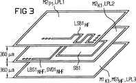
図1に示されている1つめのプリント配線板LP1は、Siemens DECT移動体“GIGASET 1000 S,C”において使用されており、製造技術的な理由から有利には片側にコンポーネントが装着されている。プリント配線板LP1は図2にその断面図が描かれているように、4つのプリント配線板レイヤLPL1〜LPL4から成る多層の第1配線板支持体LPT1を有しており、これは約1350μmの厚さであり、有利には周知のHybrid-Masslamプロセスに従って形成されている。これによればプリント配線板支持体LPT1は、厚さ約360μmの第1コアK1を有している。その際、コアK1は、その下面に配置され有利には銅製であって第1のRFグラウンド層MS1HFとして構成された第1の金属層M1K1(第3プリント配線板レイヤLPL3)と、コアK1の上面に配置され有利には銅から成る第2の金属層M2K1(第2プリント配線板レイヤLPL2)を備えている。さらに金属層M1K1,M2K1の上にはそれぞれ、厚さ約360μmである第1「プリプレグ」層P1が配置されている。この場合、ガラス繊維で増強されたエポキシ層のことを「プリプレグ」層と呼んでいる。金属層M1K1の上に配置された「プリプレグ」層P1は金属層M1K1に対向する面に、有利には銅から成る第3金属層M1P1(第4プリント配線板レイヤLPL4)を有しており、さらに金属層M2K1に対向する面に、有利には銅から成る第4金属層M2P1(第1プリント配線板レイヤLPL1)を有している。第1プリント配線板レイヤLPL1にはたとえばクリティカルなRF導体路構造LBS1HFが配置されている一方、第2プリント配線板レイヤLPL2にはたとえば第1非RF導体路構造LBS1NHFおよび/または第1非RF回路配線SVD1NHFが設けられている。第3プリント配線板レイヤLPL3におけるRFグラウンド層に関係して、導体路構造LBS1HFを非RF導体路構造LBS1NHFおよび/または第1非RF回路配線SVD1NHFによる影響から保護する目的で、第2プリント配線板レイヤLPL2にRF信号の第1フィールドライン(磁力線)FL1を広範囲にわたって取り囲む第1阻止領域SB1が設けられている。さらにプリント配線板支持体LPT1には、第1プリント配線板レイヤLPL1と第4プリント配線板レイヤLPL4との間のRFコネクションおよび非RFコネクションのための第1スルーホールDB1LPT1と、外部のモジュール(たとえばイヤホン、マイクロホンなど)の接続用の第2スルーホールDB2LPT1が設けられている。
【0005】
図3には、図2に破線で書き込まれた領域が拡大されて3次元で描かれている。
【0006】
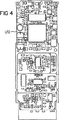
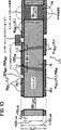
図4に示されている2つめのプリント配線板LP2は、Siemens DECT移動体“GIGASET 2000 S,C”において使用されており、これもやはり製造技術的な理由から片側にコンポーネントが装着されている。プリント配線板LP2は図5にその断面図が示されているように、やはり4つのプリント配線板レイヤLPL1〜LPL4から成り、約1350μmの厚さをもつ多層の第2プリント配線板支持体LPT2を有しており、これはやはり有利には周知のHybrid-Masslamプロセスで形成されている。これによればプリント配線板支持体LPT2は、厚さ約360μmの第2コアK2を有しており、この第2コアK2はその下面に配置され有利には銅から成る第5金属層M1K2(第3プリント配線板レイヤLPL3)と、コアK2の上面に配置され有利には銅から成り第2RFグラウンド層MS2HFとして構成された第6金属層M2K2(第2プリント配線板レイヤLPL2)を備えている。金属層M1K2,M2K2にはそれぞれ約360μmの厚さの第2「プリプレグ」層P2が配置されている。金属層M1K2上に配置された「プリプレグ」層P2は金属層M1K2に対向する面に、有利には銅から成る第6金属層M1P2(第4プリント配線板レイヤLPL4)を有しており、さらに金属層M2K2に対向する面に、有利には銅から成る第8金属層M2P2(第1プリント配線板レイヤLPL1)を有している。プリント配線板レイヤLPL2〜LPL4には、周知のトライステート構造が配置されている。この構造は、第3プリント配線板レイヤLPL3におけるクリティカルな第2RF導体路構造LBS2HF、第2プリント配線板レイヤLPL2におけるRFグラウンド層MS2HF、および第4プリント配線板レイヤLPL4においてRF信号の第2フィールドライン(磁力線)FL2のために広範囲にわたって設計された第3RFグラウンド層MS3HFによって構成されている。さらにプリント配線板支持体LPT2にはやはり、第1プリント配線板レイヤLPL1と第4プリント配線板レイヤLPL4との間のRFコネクションおよび非RFコネクションのための第1スルーホールDB1LPT2と、外部のモジュール(たとえばイヤホン、マイクロホンなど)の接続用の第2スルーホールDB2LPT2が設けられている。
【0007】
プリント配線板LP1,LP2のサイズを小さくし、ひいては(冒頭で説明したように)いっそうコンパクトなDECT移動体を製造できるようにする目的で、プリント配線板の両側にモジュールを装着させることが知られている。しかしそのためには、いっそう高い製造技術的コストが必要とされる。
【0008】
RFコンポーネントの設けられていない電気機器のプリント配線板コンセプトにおいて、電気機器の既述の小型化を促進させる目的で、周知の「マイクロビア(micro via)」技術(MV技術)を利用することが知られている。MV技術は、同様に周知の機械的なブラインドスルーホール(plating-through blind hole)の代案である。MV技術は、RF回路やRF導体路構造の設けられていないプリント配線板を低コストで製造するための接続技術である。この場合、機械的なブラインドホールの穴あけや材料の付加および除去のほかに、ホールのばり取りも不要となることで、コストが節約される。目下のところ、たとえば大面積の「マイクロビア」層を製造するために複数の製造方法が知られている。これらの方法とは、“Sequential Built Up”プロセス(SBUプロセス)、“Silver Bump”法(SB法)、プラズマエッチング法、CO2レーザによるレーザドリリング、ならびにYAGレーザによるレーザドリリングである。大規模な使用に対しては、現在の視点ではコスト的な面でおそらく最初の2つの製造方法しか考慮されない。そしてそれらの技術によって形成される「マイクロビア(micro via、スルーホール)」は、実例として50〜150μmの直径を有しており、たとえば0.12mm〜0.35mmの範囲のはんだのランドを必要とする。さらに「マイクロビア」の直径は、「マイクロビア」層(“micro via”layer)と次の層(レイヤ)との間隔に依存しており、直径/レイヤ間隔>1としなければならない。50μmの導体路幅をもつ超微細導体路技術と組み合わせて、きわめて高い配線密度が達成される。
【0009】
プリント配線板の大きさは、MV技術の代案として知られている標準技術(たとえばブラインドスルーホール)の場合、スルーホールの所要スペースやプリント配線板のコンポーネント面上に位置する導体路構造によってかなり決まってしまう。その際、MV技術によれば、コンポーネントの「パッド(pad)」においてダイレクトに第1の内部層へ「潜らせる」ことができるので、スルーホールや導体路構造のための所要スペースはほとんど重要ではなくなる。RF問題が重要視されないのであれば、製造技術的な視点で許容される範囲で密にコンポーネントを並置させることができる。MV技術の場合であるとプリント配線板のサイズは既述の条件のもとではもっぱら、使用される(構成素子)コンポーネントの個数と形状によってほとんど決まってしまう。
【0010】
本発明の課題は、電子回路や導体路構造をRFコンポーネントを備えた電気機器たとえば移動無線通信機器のための配線板に組み込む際の実装密度を高め、それによって配線板の寸法を小さくすることである。
【0011】
この課題は、請求項1の上位概念に記載の配線板において請求項1の特徴部分に記載の構成により解決される。
【0012】
本発明が基礎とする着想は以下の通りである。すなわち、プリント配線板支持体上において片側または両側にマイクロビア層が設けられており、このマイクロビア層の上に回路配線や構成素子ならびに導体路構造を有する機器固有の回路(たとえば請求項9〜12に記載された通信機器用のRF回路配線やRFコンポーネントならびにRF導体路構造を備えたRF回路あるいは非RF回路配線や非RFコンポーネントならびに非RF導体路構造を備えた非RF回路など)が、少なくとも平面の一部に取り付けられている。また、プリント配線板支持体のRFグラウンド層に関係してRF回路とRF導体路構造が、マイクロビア層のすぐ下に位置するプリント配線板支持体の支持体層に配置された阻止領域いわゆるウィンドウによって、それぞれ設定すべきRF回路ないしはRF導体路構造のRFパラメータに悪影響を及ぼす障害作用(たとえばやはりマイクロビア層のすぐ下に位置するプリント配線板支持体の支持体層の上に配置された非RF導体路構造および/または非RF回路配線)から保護されている。
【0013】
プリント配線板構造のための上述のやり方は、(上記の実施形態とは異なり)RF回路のRF回路配線およびRF導体路構造がマイクロビア層のすぐ下に位置するプリント配線板支持体の支持体層の上に配置されている一方、阻止領域ならびにRF回路のRFコンポーネント、非RF導体路構造および/または回路配線やコンポーネントを含む非RF回路がマイクロビア層の上に配置されているときも有効であるし、あるいは適用可能である。さらに、これらの構成の組み合わせも可能である。
【0014】
マイクロビア技術およびウィンドウ技術を利用する場合、プリント配線板上における回路と導体路構造の所定の実装ボリュームのために、マイクロビア技術およびウィンドウ技術を用いない技術に比べプリント配線板レイヤの数が多くなる。もっとも、プリント配線板レイヤの数は、マイクロビア技術およびウィンドウ技術を用いない技術と変わらないように抑えることもできるが、これは本発明の基礎とする課題に反して実装密度を低くしたときだけであり、これでは電気機器の所期の小型化(ミニチュア化)が達成されない。
【0015】
しかしながら、たとえば移動無線通信機器などRFコンポーネントを備えた電気機器のためのプリント配線板を、本発明で提案するやり方に従って形成するならば、機器固有の回路や導体路構造をプリント配線板に取り付けるのに必要とされるスペースが、慣用のやり方で形成されたプリント配線板よりも著しく小さくなる。
【0016】
別の実施形態によれば、マイクロビア層と、このマイクロビア層のすぐ下に位置するプリント配線板の支持体層との間の間隔が、周知のシーケンシャルビルトアッププロセス(SBUプロセス、Sequential Built Up Process)に従ってマイクロビア層を低コストで製造するのに必要なオーダにあるようにすれば有利であり、さらに実装密度が高まることからプリント配線基板の設計が小さくなることに加えて、プリント配線板の製造コストが著しく低下する。
【0017】
1つの実施形態によれば、マイクロビアのホールの直径と、マイクロビア層とマイクロビア層のすぐ下に位置するプリント配線板支持体の支持体層との間の間隔とが1よりも大きく、典型的なホールの直径が50μm〜150μmであり、はんだランド直径が0.12mm〜0.35mmである。
【0018】
請求項2〜4の実施形態によれば、プリント配線板設計を請求項1の構成よりもさらに小さくすることができる。その理由は、最初のホール(標準ビア)を覆うマイクロビア層の上に付加的に取り付けることのできるRF回路によって、実装密度をいっそう高めることができるからである。
【0019】
さらに請求項5記載の本発明の実施形態によれば、マイクロビア層における最初の穴を覆う際に、カバー処理によりホール内で発生する微環境ゆえに吹き出し(破裂)が確実に発生しないようになる。
【0020】
従属請求項には本発明の有利な実施形態が示されている。
【0021】
次に、図6〜10を参照しながら本発明の実施例について説明する。
【0022】
図6に示されている3つめのプリント配線板LP3は、MV技術をそれに適合されたウィンドウ技術といっしょに使用することで、前述のプリント配線板LP1,LP2に対し変形の施されたものであり、これは製造技術的な理由から有利にはやはり片側にコンポーネントが装着されている。もっとも、両側での装着も可能である。そのようにするならば、プリント配線板LP3のサイズがさらに小さくなるだろう。
【0023】
プリント配線板LP3は図6の断面図に示されているとおり、(プリント配線板LP1,LP2とは異なり)6つのプリント配線板レイヤLPL1〜LPL6から成る多層の第3のプリント配線板支持体LPT3を有しており、これは厚さ約1400μmであって、このうちプリント配線板レイヤLPL2〜LPL5はやはり有利には周知のHybrid-Masslamプロセスに従って形成されているのに対し、プリント配線板レイヤLPL1,LPL6はMV技術に従って形成されている。これによればプリント配線板支持体LPT3には厚さ約360μmの第3コアK3が含まれており、このコアK3はその下面に配置され有利には銅から形成された金属層M1K3と、このコアK3の上面に配置され有利には銅から成り第4RF金属層MS4HFとして構成された第10金属層M2K3(第3プリント配線板レイヤLPL3)を備えている。さらに金属層M1k3,M2K3の上にはそれぞれ、厚さ約360μmのプリプレグ層P3が配置されている。金属層M1K3上に配置されたプリプレグ層P3は金属層M1K3に対向する面上に、有利には銅から成る第11金属層M1P3(第5プリント配線板レイヤLPL5)を有しており、さらに金属層M2K3に対向する面上に、有利には銅から成る第12金属層M2P3(第2プリント配線板レイヤLPL2)を有している。
【0024】
また、金属層M1P3,M2P3上にはそれぞれ、厚さ約50μmの第1マイクロビア(micro via)層MV1が配置されている。金属層M1P3上に配置されたマイクロビア層MV1は金属層M1P3に対向する面に、有利には銅から成る第13金属層M1M1(第6プリント配線板レイヤLPL6)を有しており、さらに金属層M2P3に対向する面に、有利には銅から成る第14金属層M2M1(第1プリント配線板レイヤLPL1)を有している。第1プリント配線板レイヤLPL1にはたとえばクリティカルな第2RF導体路構造LBS2HFが配置されているのに対し、第2プリント配線板レイヤLPL2にはたとえば第2非RF導体路構造LBS2NHFおよび/または第2非RF回路配線SVD2NFHが設けられている。第3プリント配線板レイヤLPL3内におけるRFグラウンド層MS4HFと関係してRF導体路構造LBS2HFを、非RF導体路構造LBSNHFおよび/または非RF回路配線SVD2NHFによる影響から保護する目的で、第2プリント配線板レイヤLPL2内に、RF信号の第3フィールドライン(磁力線)FL3を広範囲にわたって取り囲む第3阻止領域SB3が設けられている。
【0025】
RF導体路構造LBS2HFを択一的および/または付加的に、第2プリント配線板レイヤLPL2、第5プリント配線板レイヤLPL5、および/または第6プリント配線板レイヤLPL6内に配置させてもよい。最後の事例であれば、矛盾のないよう第5プリント配線板レイヤLPL5内に阻止領域が配置されていなければならない。また、最初の2つの事例であれば、第1プリント配線板レイヤLPL1または第6プリント配線板レイヤLPL6内に阻止領域が設けられることになる。
【0026】
さらにプリント配線板支持体LPT3には、第1プリント配線板レイヤLPL1と第6プリント配線板レイヤLPL6との間のRFコネクションおよび非RFコネクションのための第1スルーホールDB1LPT3と、外部のモジュール(たとえばイヤホン、マイクロホンなど)の接続用の第2スルーホールDB2LPT3が設けられている。図示されているようにスルーホールDB1LPT3が開放されたままであればそれらのホールから、プリント配線板上のRF回路やRF導体路構造により引き起こされるRF放射が漏れ出てくる(望ましくない作用)。図7には、図6に破線で書き込んだ領域が拡大されて3次元表示で描かれている。
【0027】
図8には、図6に示したプリント配線板LP3に対し若干変形された4つめのプリント配線板LP3が示されており、これもやはり製造技術的な理由から有利には片側にコンポーネントが装着されている。この場合も両側に装着させることができる。このプリント配線板LP4は図8の断面図に描かれているように、6つのプリント配線板レイヤLPL1〜LPL6から成る多層の第4プリント配線板支持体LPT4を有しており、これは厚さ約1400μmであって、このうちプリント配線板レイヤLPL2〜LPL5はやはり有利には周知のHybrid-Masslamプロセスに従って形成されているのに対し、プリント配線板レイヤLPL1,LPL6はMV技術に従って形成されている。
【0028】
これによればプリント配線板支持体LPT4は厚さ約360μmの第4コアK4を有しており、このコアK4はその下面に配置され有利には銅から成る第15金属層M1K4(第4プリント配線板レイヤLPL4)と、このコアK4の上面に配置され有利には銅から成り第5RFグラウンド層MS5HFとして構成された第16金属層M2K4(第3プリント配線板レイヤLPL3)を備えている。金属層M1K4,M2K4の上にはそれぞれ、厚さ約360μmの第4プリプレグ層P4が配置されている。金属層M1K4の上に配置されたプリプレグ層4は金属層M1K4に対向する面に、有利には銅から成る第16金属層M1P4(第5プリント配線板レイヤLPL5)を有しており、さらに金属層M2K4に対向する面に、有利には銅から成る第18金属層M2P4(第2プリント配線板レイヤLPL2)を有している。金属層M1P4,M1P4上にはそれぞれ、厚さ約50μmの第2マイクロビア層MV2が配置されている。また、金属層M1P4上に配置されたマイクロビア層MV2は金属層M1P4に対向する面に、有利には銅から成る第19金属層M1M2(第6プリント配線板レイヤLPL6)を有しており、さらに金属層M2P4に対向する面には、有利には銅から成る第14金属層M2M2(第1プリント配線板レイヤLPL1)を有している。
【0029】
第1プリント配線板レイヤLPL1にはたとえばクリティカルな第3RF導体路構造LBS3HFが配置されているのに対し、第2プリント配線板レイヤLPL2にはたとえば第3非RF導体路構造LBS3NHFおよび/または第3非RF回路配線SVD3NHFが設けられている。第3プリント配線板レイヤLPL3におけるRFグラウンド層MS5HFに関係してRF構造体導体路LBS3HFを、非RF導体路構造LBS3NHFおよび/または非RF回路配線SVD3NHFによる影響から保護する目的で、第2プリント配線板レイヤLPL2にRF信号の第4フィールドラインFL4を広範囲に取り囲む第4阻止領域SB4が設けられている。
【0030】
やはりRF導体路構造LBS3HFも、択一的または付加的に第2プリント配線板レイヤLPL2、第5プリント配線板レイヤLPL5、および/または第6プリント配線板レイヤLPL6に配置させることができる。最後の事例であれば、矛盾のないよう第5プリント配線板レイヤLPL5内に阻止領域が配置されていなければならない。また、最初の2つの事例であれば、第1プリント配線板レイヤLPL1または第6プリント配線板レイヤLPL6内に阻止領域が設けられることになる。
【0031】
さらにプリント配線板支持体LPT4には、第1プリント配線板レイヤLPL1と第6プリント配線板レイヤLPL6との間のRFコネクションおよび非RFコネクションのための第1スルーホールDB1LPT4と、外部のモジュール(たとえばイヤホン、マイクロホンなど)の接続用の第2スルーホールDB2LPT4が設けられている。図6の場合と異なりスルーホールDB1LPT4は、図示されているようにマイクロビア層MV2を介して金属層M1M2または金属層M2M2と接続されている。金属層M2M2では、この処置によりRF回路またはRF導体路構造のための付加的なスペースが得られる一方、金属層M1M2ではこれが連続的なグラウンド層として形成されることで、ホールが「RF密に」あるいはRFを通さないようにされていて、その結果、このホール開口部からはプリント配線板上のRF回路やRF導体路により引き起こされるRF放射が漏れ出てくる可能性がもはやなくなる。他のホール開口部の上にはRF回路またはRF導体路構造が配置されているので、そこから漏れ出るRF放射はクリティカルなものではない。
【0032】
このようにしてカバーされるホールDBLPT4が、覆われるときにこのことでホールから発生する微環境によって吹き出されないようにする目的で、ホールは有利には充填材料で充填される。
【0033】
図9には、このようにして実現可能なプリント配線板LP4の大きさが示されている。
【0034】
さらに図10には、択一的な実施形態が示されている。図6〜図8に示した実施形態とは異なり、2つのマイクロビア層を考慮していないプリント配線板支持体は、単一の支持体層によって構成されている。これによって、プリント配線板支持体構造に関して製造コストの低減が実現される。
【図面の簡単な説明】
【図1】Siemens DECT移動体“GIGASET 1000 S,C”において使用されているプリント配線板を示す図
【図2】図1に描かれたプリント配線板の断面図
【図3】図2に破線で書き込まれた領域を拡大して3次元で示す図
【図4】Siemens DECT移動体“GIGASET 2000 S,C”において使用されているプリント配線板を示す図
【図5】図4に描かれたプリント配線板の断面図
【図6】本発明の1つの実施形態を示す図
【図7】図6に破線で書き込んだ領域を拡大して3次元表示で示す図
【図8】図6に示したプリント配線板に対し若干変形された4つめのプリント配線板を示す図
【図9】実現可能なプリント配線板の大きさを示す図
【図10】プリント配線板の択一的な実施形態を示す図[0001]
The present invention relates to a printed wiring board for an electric device having an RF component according to the superordinate concept of claim 1, for example, a mobile radio communication device.
[0002]
In the case of electrical equipment having high-frequency components or high-frequency device parts (RF components, RF devices), these high-frequency components and non-high-frequency components must be separated from the interaction between the components, or from each other It must be protected from affecting each other [(1): When the low-frequency component is closely arranged with respect to the high-frequency component, the low-frequency characteristic of the low-frequency component is affected by the high-frequency signal; (2 The high frequency component is affected with respect to the high frequency parameter setting by the low frequency (AF) component located close to the high frequency (RF) component. Typical locations where both RF components (RF circuits with RF wiring and RF components) and non-RF components (non-RF circuits with non-RF wiring and non-RF components) are closely packed are arranged in electrical equipment. It is a printed wiring board or an electronic flat module. Moreover, in the case of a small device having a small wiring board, the interaction that causes a failure between the components becomes more intense. On the other hand, there is an increasing demand for smaller and more compact electrical equipment. This is especially the case where a miniaturized device can be made portable, that is, a user can take the miniaturized device almost anywhere (any geographical location). It is. Such a small portable device is, for example, a mobile radio communication device.
[0003]
For example, a number of (mobile) wireless communication devices used for message transmission for various purposes such as voice, packet and / or image data, such as DECT communication devices, GSM communication devices, Personal Handyphone System communication devices, so-called PHS communication devices, “IS -95 "communication equipment, as well as communication equipment based on single or multiple transmission schemes (eg DS-CDMA or JD-CDMA) with basic transmission schemes FDMA, TDMA, CDMA (for example the above mentioned problems) On the other hand, on the other hand, miniaturization and on the other hand, the requirement for avoiding interaction between the RF component and the AF component is coupled with the requirement for equipment with lower costs <keyword: mass production>. Below) for all the devices listed here. As, we will be going to describe the operation of generating a DECT mobile illustratively.
[0004]
The first printed circuit board LP1 shown in FIG. 1 is used in the Siemens DECT mobile “GIGASET 1000 S, C”, and is advantageously equipped with components on one side for manufacturing technical reasons. . The printed wiring board LP1 has a multilayer first wiring board support LPT1 composed of four printed wiring board layers LPL1 to LPL4, as shown in the sectional view of FIG. 2, which is about 1350 μm. Thickness, preferably formed according to the well-known Hybrid-Masslam process. According to this, the printed wiring board support LPT1 has a first core K1 having a thickness of about 360 μm. In this case, the core K1 is disposed on the lower surface of the first metal layer M1 K1 (third printed wiring board layer LPL3), which is preferably made of copper and configured as the first RF ground layer MS1 HF , A second metal layer M2 K1 (second printed wiring board layer LPL2), preferably made of copper, is provided on the upper surface of K1. Further, a first “prepreg” layer P1 having a thickness of about 360 μm is disposed on each of the metal layers M1 K1 and M2 K1 . In this case, the epoxy layer reinforced with glass fibers is called the “prepreg” layer. "Prepreg" layer P1 arranged on the metal layer M1 K1 is on a surface facing the metal layer M1 K1, advantageously has a third metal layer M1 P1 (Fourth printed wiring board layers LPL4) made of copper Furthermore, a fourth metal layer M2 P1 (first printed wiring board layer LPL1), preferably made of copper, is provided on the surface facing the metal layer M2 K1 . The first printed wiring board layer LPL1 is provided with, for example, a critical RF conductor path structure LBS1 HF, while the second printed wiring board layer LPL2 is provided with, for example, a first non-RF conductor path structure LBS1 NHF and / or a first non-wire structure. RF circuit wiring SVD1 NHF is provided. For the purpose of protecting the conductor path structure LBS1 HF from the influence of the non-RF conductor path structure LBS1 NHF and / or the first non-RF circuit line SVD1 NHF in relation to the RF ground layer in the third printed wiring board layer LPL3, the second The printed wiring board layer LPL2 is provided with a first blocking region SB1 that surrounds the first field line (line of magnetic force) FL1 of the RF signal over a wide range. Further, the printed wiring board support LPT1 includes a first through hole DB1 LPT1 for RF connection and non-RF connection between the first printed wiring board layer LPL1 and the fourth printed wiring board layer LPL4, and an external module ( For example, a second through hole DB2 LPT1 for connecting an earphone, a microphone, etc.) is provided.
[0005]
In FIG. 3, the region written with a broken line in FIG. 2 is enlarged and drawn in three dimensions.
[0006]
The second printed wiring board LP2 shown in FIG. 4 is used in the Siemens DECT mobile “GIGASET 2000 S, C”, which also has components mounted on one side for manufacturing engineering reasons. . As shown in the sectional view of FIG. 5, the printed wiring board LP2 is composed of four printed wiring board layers LPL1 to LPL4, and has a multilayer second printed wiring board support LPT2 having a thickness of about 1350 μm. Which is also advantageously formed by the well-known Hybrid-Masslam process. According to this, the printed wiring board support LPT2 has a second core K2 having a thickness of about 360 μm, and this second core K2 is arranged on its lower surface and is preferably a fifth metal layer M1 K2 made of copper. (Third printed wiring board layer LPL3) and a sixth metal layer M2 K2 (second printed wiring board layer LPL2) arranged on the upper surface of the core K2 and preferably made of copper and configured as a second RF ground layer MS2 HF I have. A second “prepreg” layer P2 having a thickness of about 360 μm is disposed on each of the metal layers M1 K2 and M2 K2 . Metal layer M1 K2 disposed on "prepreg" layer P2 on the surface facing the metal layer M1 K2, advantageously has a sixth metal layer M1 P2 (fourth printed circuit board layer LPL4) made of copper In addition, an eighth metal layer M2 P2 (first printed wiring board layer LPL1) preferably made of copper is provided on the surface facing the metal layer M2 K2 . A well-known tri-state structure is arranged on the printed wiring board layers LPL2 to LPL4. This structure is based on the critical second RF conductor path structure LBS2 HF in the third printed wiring board layer LPL3, the RF ground layer MS2 HF in the second printed wiring board layer LPL2, and the second RF signal in the fourth printed wiring board layer LPL4. It is constituted by a third RF ground layer MS3 HF designed extensively for the field line (field line) FL2. Further, the printed wiring board support LPT2 also includes a first through hole DB1 LPT2 for RF connection and non-RF connection between the first printed wiring board layer LPL1 and the fourth printed wiring board layer LPL4, and an external module. A second through hole DB2 LPT2 for connection (for example, an earphone, a microphone, etc.) is provided.
[0007]
It is known that modules are mounted on both sides of a printed wiring board in order to reduce the size of the printed wiring boards LP1 and LP2 and thus to make a more compact DECT mobile (as explained at the beginning). ing. However, this requires higher manufacturing technology costs.
[0008]
In a printed wiring board concept of an electric device not provided with an RF component, the well-known “micro via” technology (MV technology) may be used for the purpose of promoting the downsizing of the electric device described above. Are known. MV technology is also an alternative to the well-known mechanical-plating-through blind hole. The MV technique is a connection technique for manufacturing a printed wiring board not provided with an RF circuit or an RF conductor path structure at a low cost. In this case, in addition to mechanical blind hole drilling and material addition and removal, hole deburring is not required, thereby saving costs. Currently, a number of manufacturing methods are known, for example to manufacture large area “microvia” layers. These methods are “Sequential Built Up” process (SBU process), “Silver Bump” method (SB method), plasma etching method, laser drilling by CO 2 laser, and laser drilling by YAG laser. For large-scale use, only the first two manufacturing methods are probably considered in terms of cost from the current point of view. The “micro via” formed by these techniques has a diameter of 50 to 150 μm as an example, and requires a solder land in the range of 0.12 mm to 0.35 mm, for example. And Furthermore, the diameter of the “microvia” depends on the spacing between the “micro via” layer and the next layer, and the diameter / layer spacing must be> 1. In combination with ultrafine conductor track technology with a conductor track width of 50 μm, very high wiring densities are achieved.
[0009]
In the case of a standard technology (for example, blind through hole) known as an alternative to the MV technology, the size of the printed wiring board is considerably determined by the required space of the through hole and the conductor path structure located on the component surface of the printed wiring board. End up. In that case, according to the MV technology, the “pad” of the component can be “hidden” directly to the first inner layer, so the required space for through-holes and conductor track structures is hardly important Disappear. If the RF problem is not regarded as important, the components can be closely juxtaposed within the range allowed from the viewpoint of manufacturing technology. In the case of the MV technology, the size of the printed wiring board is almost determined by the number and shape of the (component) components used under the above-described conditions.
[0010]
An object of the present invention is to increase the mounting density when incorporating an electronic circuit or a conductor path structure into a wiring board for an electric device having an RF component, for example, a mobile radio communication device, thereby reducing the size of the wiring board. is there.
[0011]
This problem is solved by the configuration described in the characterizing portion of claim 1 in the wiring board described in the superordinate concept of claim 1.
[0012]
The idea on which the present invention is based is as follows. That is, a micro via layer is provided on one side or both sides on a printed wiring board support, and a circuit unique to a device having circuit wiring, a component, and a conductor path structure on the micro via layer (for example, claims 9 to 9). RF circuit wiring and RF components for communication equipment described in 12 or RF circuit having RF conductor path structure or non-RF circuit wiring and non-RF circuit having non-RF component and non-RF conductor path structure). It is attached to at least a part of the plane. In addition, an RF circuit and an RF conductor path structure related to the RF ground layer of the printed wiring board support are arranged in a blocking region so-called window arranged in the support layer of the printed wiring board support located immediately below the micro via layer. By means of obstacles which adversely affect the RF parameters of the RF circuit or RF conductor path structure to be set respectively (for example, non-concentrations arranged on the support layer of the printed wiring board support located immediately below the micro via layer). RF conductor track structure and / or non-RF circuit wiring).
[0013]
The above-described manner for the printed wiring board structure (unlike the above embodiment) is the support of the printed wiring board support in which the RF circuit wiring and the RF conductor path structure of the RF circuit are located immediately below the micro via layer. It is also effective when placed on the micro-via layer while placed on the layer, while non-RF circuits, including blocking regions and RF circuit RF components, non-RF conductor track structures and / or circuit wiring and components Or is applicable. Furthermore, a combination of these configurations is also possible.
[0014]
When using micro via technology and window technology, the number of printed wiring board layers is larger than the technology that does not use micro via technology and window technology due to the predetermined mounting volume of the circuit and conductor structure on the printed wiring board. Become. Of course, the number of printed wiring board layers can be kept the same as the technology that does not use the micro via technology and window technology, but this is only when the mounting density is lowered against the basic problem of the present invention. Thus, the desired miniaturization (miniaturization) of electrical equipment cannot be achieved.
[0015]
However, if a printed wiring board for an electric device having an RF component such as a mobile radio communication device is formed according to the method proposed in the present invention, a circuit or a conductor path structure unique to the device is attached to the printed wiring board. The required space is significantly smaller than a printed wiring board formed in a conventional manner.
[0016]
According to another embodiment, the spacing between the microvia layer and the printed wiring board support layer located directly below the microvia layer is a well-known sequential built-up process (SBU process, Sequential Built Up). It is advantageous to make the microvia layer on the order required to manufacture the microvia layer at a low cost according to (Process), and in addition to the fact that the printed wiring board design becomes smaller due to the increased mounting density, the printed wiring board The manufacturing cost is significantly reduced .
[0017]
According to one embodiment, the diameter of the microvia hole and the spacing between the microvia layer and the support layer of the printed wiring board support located directly below the microvia layer is greater than 1, Typical hole diameters are 50 μm to 150 μm and solder land diameters are 0.12 mm to 0.35 mm.
[0018]
According to the embodiments of claims 2 to 4 , the printed wiring board design can be made smaller than the configuration of claim 1. The reason is that the mounting density can be further increased by an RF circuit that can be additionally mounted on the microvia layer covering the first hole (standard via).
[0019]
Furthermore, according to the embodiment of the present invention as set forth in claim 5, when the first hole in the micro via layer is covered, blowout (burst) is not reliably generated due to the microenvironment generated in the hole by the cover processing. .
[0020]
The dependent claims contain advantageous embodiments of the invention.
[0021]
Next, an embodiment of the present invention will be described with reference to FIGS.
[0022]
The third printed wiring board LP3 shown in FIG. 6 is a modification of the above-described printed wiring boards LP1 and LP2 by using the MV technology together with the window technology adapted thereto. Yes, this is also advantageous for manufacturing technical reasons, again with components mounted on one side. However, it can be mounted on both sides. If so, the size of the printed wiring board LP3 will be further reduced.
[0023]
As shown in the sectional view of FIG. 6, the printed wiring board LP3 (unlike the printed wiring boards LP1 and LP2) is a multilayer third printed wiring board support LPT3 composed of six printed wiring board layers LPL1 to LPL6. Which has a thickness of about 1400 μm, among which the printed wiring board layers LPL2 to LPL5 are advantageously formed according to the well-known Hybrid-Masslam process, whereas the printed wiring board layer LPL1 , LPL6 is formed according to MV technology. According to this, the printed wiring board support LPT3 includes a third core K3 having a thickness of about 360 μm, and this core K3 is disposed on the lower surface thereof, and preferably a metal layer M1 K3 made of copper, A tenth metal layer M2 K3 (third printed wiring board layer LPL3) is disposed on the upper surface of the core K3 and is preferably made of copper and configured as a fourth RF metal layer MS4 HF . Further, a prepreg layer P3 having a thickness of about 360 μm is disposed on each of the metal layers M1 k3 and M2 K3 . Metal layer M1 K3 prepreg layers P3 disposed on the on the surface facing the metal layer M1 K3, advantageously has an eleventh metal layer M1 P3 (fifth printed wiring board layers LPL5) made of copper Further, a twelfth metal layer M2 P3 (second printed wiring board layer LPL2), preferably made of copper, is provided on the surface facing the metal layer M2 K3 .
[0024]
A first micro via layer MV1 having a thickness of about 50 μm is disposed on each of the metal layers M1 P3 and M2 P3 . Microvia layer MV1 placed on the metal layer M1 P3 is on a surface facing the metal layer M1 P3, and advantageously has a first 13 metal layer M1 M1 (Sixth printed wiring board layers LPL6) made of copper Furthermore, a 14th metal layer M2 M1 (first printed wiring board layer LPL1), preferably made of copper, is provided on the surface facing the metal layer M2 P3 . For example, the critical second RF conductor path structure LBS2 HF is arranged in the first printed wiring board layer LPL1, whereas the second non-RF conductor path structure LBS2 NHF and / or in the second printed wiring board layer LPL2 Second non-RF circuit wiring SVD2 NFH is provided. In order to protect the RF conductor path structure LBS2 HF in relation to the RF ground layer MS4 HF in the third printed wiring board layer LPL3 from the influence of the non-RF conductor path structure LBS NHF and / or the non-RF circuit wiring SVD2 NHF , In the second printed wiring board layer LPL2, a third blocking region SB3 that surrounds the third field line (line of magnetic force) FL3 of the RF signal over a wide range is provided.
[0025]
The RF conductor path structure LBS2 HF may alternatively and / or additionally be disposed in the second printed wiring board layer LPL2, the fifth printed wiring board layer LPL5, and / or the sixth printed wiring board layer LPL6. . In the last case, a blocking area must be arranged in the fifth printed wiring board layer LPL5 so that there is no contradiction. In the first two cases, a blocking region is provided in the first printed wiring board layer LPL1 or the sixth printed wiring board layer LPL6.
[0026]
Further, the printed wiring board support LPT3 includes a first through hole DB1 LPT3 for RF connection and non-RF connection between the first printed wiring board layer LPL1 and the sixth printed wiring board layer LPL6, and an external module ( For example, a second through hole DB2 LPT3 for connecting an earphone, a microphone, etc.) is provided. As shown in the figure, if the through holes DB1 LPT3 remain open, RF radiation caused by the RF circuit or the RF conductor path structure on the printed wiring board leaks out from these holes (undesired effect). In FIG. 7, the region written with a broken line in FIG. 6 is enlarged and drawn in a three-dimensional display.
[0027]
FIG. 8 shows a fourth printed wiring board LP3 that is slightly modified with respect to the printed wiring board LP3 shown in FIG. 6, which is also advantageously mounted on one side for manufacturing technical reasons. Has been. In this case, it can be mounted on both sides. The printed wiring board LP4 has a multilayer fourth printed wiring board support LPT4 composed of six printed wiring board layers LPL1 to LPL6 as shown in the sectional view of FIG. Of these, the printed wiring board layers LPL2 to LPL5 are advantageously formed according to the well-known Hybrid-Masslam process, whereas the printed wiring board layers LPL1 and LPL6 are formed according to the MV technique. .
[0028]
According to this, the printed wiring board support LPT4 has a fourth core K4 having a thickness of about 360 μm, and this core K4 is arranged on the lower surface thereof and is preferably a fifteenth metal layer M1 K4 (fourth made of copper). A printed wiring board layer LPL4) and a sixteenth metal layer M2 K4 (third printed wiring board layer LPL3) which is arranged on the upper surface of the core K4 and is preferably made of copper and configured as a fifth RF ground layer MS5 HF. Yes. A fourth prepreg layer P4 having a thickness of about 360 μm is disposed on each of the metal layers M1 K4 and M2 K4 . The surface the prepreg layer 4 disposed on the metal layer M1 K4 is opposed to the metal layer M1 K4, advantageously has a sixteenth metal layer M1 P4 (fifth printed wiring board layers LPL5) made of copper Further, an 18th metal layer M2 P4 (second printed wiring board layer LPL2) made of copper is provided on the surface facing the metal layer M2 K4 . A second micro via layer MV2 having a thickness of about 50 μm is disposed on each of the metal layers M1 P4 and M1 P4 . The micro via layer MV2 placed on the metal layer M1 P4 is on a surface facing the metal layer M1 P4, advantageously has a first 19 metal layer M1 M2 (Sixth printed wiring board layers LPL6) made of copper Furthermore, on the surface facing the metal layer M2 P4 , there is preferably a fourteenth metal layer M2 M2 (first printed wiring board layer LPL1) made of copper.
[0029]
For example, a critical third RF conductor path structure LBS3 HF is disposed in the first printed wiring board layer LPL1, whereas, for example, the third non-RF conductor path structure LBS3 NHF and / or in the second printed wiring board layer LPL2 Third non-RF circuit wiring SVD3 NHF is provided. In order to protect the RF structure conductor path LBS3 HF from the influence of the non-RF conductor path structure LBS3 NHF and / or the non-RF circuit wiring SVD3 NHF in relation to the RF ground layer MS5 HF in the third printed wiring board layer LPL3, The second printed wiring board layer LPL2 is provided with a fourth blocking area SB4 surrounding the fourth field line FL4 of the RF signal over a wide range.
[0030]
Again, the RF conductor path structure LBS3 HF can be alternatively or additionally arranged in the second printed wiring board layer LPL2, the fifth printed wiring board layer LPL5, and / or the sixth printed wiring board layer LPL6. In the last case, a blocking area must be arranged in the fifth printed wiring board layer LPL5 so that there is no contradiction. In the first two cases, a blocking region is provided in the first printed wiring board layer LPL1 or the sixth printed wiring board layer LPL6.
[0031]
Further, the printed wiring board support LPT4 includes a first through hole DB1 LPT4 for RF connection and non-RF connection between the first printed wiring board layer LPL1 and the sixth printed wiring board layer LPL6, and an external module ( For example, a second through hole DB2 LPT4 for connecting an earphone, a microphone, etc.) is provided. Unlike the case of FIG. 6, the through hole DB1 LPT4 is connected to the metal layer M1 M2 or the metal layer M2 M2 through the micro via layer MV2 as shown. In the metal layer M2 M2 , this procedure provides additional space for the RF circuit or RF conductor track structure, while in the metal layer M1 M2 , this is formed as a continuous ground layer, so that the holes are “RF As a result, there is no longer any possibility that RF radiation caused by the RF circuit or the RF conductor path on the printed wiring board leaks from the hole opening. Since the RF circuit or RF conductor track structure is placed over the other hole opening, the RF radiation leaking from it is not critical.
[0032]
In order to prevent the hole DB LPT4 covered in this way from being blown out by the microenvironment generated from the hole when this is covered, the hole is preferably filled with a filling material.
[0033]
FIG. 9 shows the size of the printed wiring board LP4 that can be realized in this way.
[0034]
Further, in FIG. 10, an alternative embodiment is shown. Unlike the embodiment shown in FIGS. 6 to 8, the printed wiring board support that does not consider the two microvia layers is constituted by a single support layer. This realizes a reduction in manufacturing cost for the printed wiring board support structure.
[Brief description of the drawings]
1 is a diagram showing a printed wiring board used in a Siemens DECT mobile “GIGASET 1000 S, C”. FIG. 2 is a cross-sectional view of the printed wiring board depicted in FIG. 1. FIG. 3 is a broken line in FIG. Fig. 4 is an enlarged view of the area written in 3D. Fig. 4 shows a printed circuit board used in the Siemens DECT mobile "GIGASET 2000 S, C". Fig. 5 is drawn in Fig. 4. FIG. 6 is a cross-sectional view of a printed wiring board. FIG. 6 is a view showing one embodiment of the present invention. FIG. 7 is an enlarged view of a region written by a broken line in FIG. FIG. 9 is a diagram showing a size of a printed wiring board that can be realized. FIG. 10 is an alternative embodiment of the printed wiring board. Illustration
Claims (4)
a)第1の外側層(LPL2)と第2の外側層(LPL3,LPL5)を備えたプリント配線板支持体(LPT3〜LPT5)が設けられており、該プリント配線板支持体は、前記の外側層(LPL2,LPL3,LPL5)を貫通する複数のホール(DB1LPT3〜5,DB2LPT3〜5)を有しており、
b)マイクロビア層(MV1〜MV3)が設けられており、該マイクロビア層は両方の外側層(LPL2,LPL3,LPL5)のうち少なくとも一方の外側層(LPL2,LPL3,LPL5)の上に少なくとも部分的に被着されており、ここでマイクロビアの直径と、前記マイクロビア層(MV1〜MV3)の厚さとの比は1よりも大きく、前記マイクロビアの直径は50μm〜150μmの範囲にあり、
c)前記マイクロビア層(MV1〜MV3)に、または前記マイクロビア層によりそれぞれ覆われた外側層(LPL2,LPL3,LPL5)に非RF回路および非RF導体路構造(LBS2NHF〜LBS4NHF)のための阻止領域(SB2〜SB4)が設けられており、該阻止領域(SB〜SB4)は、前記プリント配線板支持体(LPT3〜LPT5)のRFグラウンド層(LPL3,MS4HF〜MS6HF)につらなるRF信号の磁力線を広範囲にわたって取り囲むウィンドウにより形成され、前記阻止領域(SB2〜SB4)の上方または下方に位置するプリント配線板レイヤに配置されたRF回路およびRF導体路構造(LBS3HF〜LBS5HF)のRF特性が保護されており、
d)プリント配線板が組み立てられた状態で前記マイクロビア層(MV1〜MV3)の上にRF回路および非RF回路のコンポーネントが配置されており、
e)少なくとも前記マイクロビア層(MV1〜MV3)に、または前記マイクロビア層(MV1〜MV3)によりそれぞれ覆われた外側層(LPL2,LPL3,LPL5)に、回路の配線(SVD2NHF〜SVD4NHF)が配置されており、
f)少なくとも前記マイクロビア層(MV1〜MV3)に、または前記マイクロビア層(MV1〜MV3)によりそれぞれ覆われた外側層(LPL2,LPL3,LPL5)に、導体路構造(LBS2NHF〜LBS4NHF,LBS3HF〜LBS5HF)が配置されていることを特徴とする、
RFコンポーネントを備えた電気機器のためのプリント配線板。For electrical equipment with RF components, eg mobile radio communication equipment, of the type in which RF circuits, non-RF circuits, RF conductor track structures and non-RF conductor track structures are arranged on printed wiring boards (LP3 to LP5) In the printed wiring board of
a) A printed wiring board support (LPT3 to LPT5) having a first outer layer (LPL2) and a second outer layer (LPL3, LPL5) is provided. A plurality of holes (DB1 LPT3 to 5 , DB2 LPT3 to 5) penetrating the outer layers (LPL2, LPL3, LPL5);
b) Micro via layers (MV1 to MV3) are provided, and the micro via layers are provided on at least one outer layer (LPL2, LPL3, LPL5) of both outer layers (LPL2, LPL3, LPL5). It is partially applied, wherein the micro-via diameter, the ratio of the thickness before Symbol microvia layer (MV1~MV3) greater than 1, the diameter of the microvias range 50μm~150μm And
in c) the microvia layer (MV1~MV3), an outer layer covered respectively by the microvia layer was or (LPL2, LPL3, LPL5) to the non-RF circuits and non-RF conductor track structures (LBS2 NHF ~LBS4 NHF ) Are provided , and the blocking areas (SB2 to SB4) are RF ground layers (LPL3, MS4 HF to MS6 HF ) of the printed wiring board support (LPT3 to LPT5). ) in continuous it is formed by the window surrounding extensively magnetic field lines of the RF signal, the blocking region (RF circuits and RF conductor path structure disposed above or printed circuit board layers located below the SB2~SB4) (LBS3 HF ~ LBS5 HF ) RF characteristics are protected,
d) RF circuit and non-RF circuit components are disposed on the microvia layer (MV1 to MV3) in a state where the printed wiring board is assembled;
to e) at least the microvia layer (MV1~MV3), the outer layer covered respectively by the microvia layer was or (MV1~MV3) (LPL2, LPL3, LPL5), circuit wiring (SVD2 NHF ~SVD4 NHF ) is located,
to f) at least the microvia layer (MV1~MV3), the outer layer or is covered respectively by the microvia layer (MV1~MV3) (LPL2, LPL3, LPL5), conductor track structures (LBS2 NHF ~LBS4 NHF , LBS3 HF to LBS5 HF ) are arranged,
Printed wiring boards for electrical equipment with RF components.
Applications Claiming Priority (1)
| Application Number | Priority Date | Filing Date | Title |
|---|---|---|---|
| PCT/DE1997/000490 WO1998041066A1 (en) | 1997-03-12 | 1997-03-12 | Circuit board for electrical apparatus with hf components, particularly for mobile radiocommunications equipment |
Related Child Applications (1)
| Application Number | Title | Priority Date | Filing Date |
|---|---|---|---|
| JP2003362195A Division JP2004119986A (en) | 2003-10-22 | 2003-10-22 | Print distribution plate for electrical equipment provided with rf component such as mobile radiocommunication apparatus |
Publications (2)
| Publication Number | Publication Date |
|---|---|
| JP2000513151A JP2000513151A (en) | 2000-10-03 |
| JP4072207B2 true JP4072207B2 (en) | 2008-04-09 |
Family
ID=6918477
Family Applications (1)
| Application Number | Title | Priority Date | Filing Date |
|---|---|---|---|
| JP53903398A Expired - Lifetime JP4072207B2 (en) | 1997-03-12 | 1997-03-12 | Printed wiring board for electrical equipment with RF components, eg mobile radio communication equipment |
Country Status (12)
| Country | Link |
|---|---|
| US (1) | US6370034B1 (en) |
| EP (1) | EP0956747B1 (en) |
| JP (1) | JP4072207B2 (en) |
| KR (1) | KR100393243B1 (en) |
| AT (1) | ATE206579T1 (en) |
| AU (1) | AU725291B2 (en) |
| BR (1) | BR9714669B1 (en) |
| CA (1) | CA2283150C (en) |
| DE (1) | DE59704821D1 (en) |
| ES (1) | ES2166532T3 (en) |
| HK (1) | HK1026808A1 (en) |
| WO (1) | WO1998041066A1 (en) |
Families Citing this family (11)
| Publication number | Priority date | Publication date | Assignee | Title |
|---|---|---|---|---|
| JP2002164465A (en) * | 2000-11-28 | 2002-06-07 | Kyocera Corp | Wiring board, wiring board, their mounted board, and multi-chip module |
| TWM248187U (en) * | 2003-01-15 | 2004-10-21 | Abocom Sys Inc | Printed circuit board structure of RF transmission device |
| RU2009111002A (en) * | 2006-08-27 | 2010-10-10 | Май Мобайл Вотч Лимитед (Cn) | MOBILE WATCH PHONE FOR GSM SYSTEM |
| US8994182B2 (en) | 2012-12-21 | 2015-03-31 | Cree, Inc. | Dielectric solder barrier for semiconductor devices |
| US8970010B2 (en) | 2013-03-15 | 2015-03-03 | Cree, Inc. | Wafer-level die attach metallization |
| JP6599853B2 (en) | 2013-06-21 | 2019-10-30 | サンミナ コーポレーション | Method of forming a laminated structure having plated through holes using a removable cover layer |
| US10881001B2 (en) | 2017-03-02 | 2020-12-29 | Flex Ltd. | Micro conductive thread interconnect component to make an interconnect between conductive threads in fabrics to PCB, FPC, and rigid-flex circuits |
| US10535845B1 (en) | 2017-07-14 | 2020-01-14 | Flex Ltd. | Flexible and stretchable chain battery |
| US10426029B1 (en) * | 2018-01-18 | 2019-09-24 | Flex Ltd. | Micro-pad array to thread flexible attachment |
| US10687421B1 (en) | 2018-04-04 | 2020-06-16 | Flex Ltd. | Fabric with woven wire braid |
| US10575381B1 (en) | 2018-06-01 | 2020-02-25 | Flex Ltd. | Electroluminescent display on smart textile and interconnect methods |
Family Cites Families (9)
| Publication number | Priority date | Publication date | Assignee | Title |
|---|---|---|---|---|
| US4402998A (en) * | 1982-01-04 | 1983-09-06 | Western Electric Co., Inc. | Method for providing an adherent electroless metal coating on an epoxy surface |
| US5768109A (en) * | 1991-06-26 | 1998-06-16 | Hughes Electronics | Multi-layer circuit board and semiconductor flip chip connection |
| US5357225A (en) * | 1992-12-23 | 1994-10-18 | Alcatel Network Systems, Inc. | Method and apparatus for adjusting the impedance of a microstrip transmission line |
| WO1994022531A1 (en) * | 1993-03-31 | 1994-10-13 | Motorola Inc. | Switch circuit and method therefor |
| US5451720A (en) * | 1994-03-23 | 1995-09-19 | Dell Usa, L.P. | Circuit board thermal relief pattern having improved electrical and EMI characteristics |
| FI102121B (en) * | 1995-04-07 | 1998-10-15 | Filtronic Lk Oy | Transmitter / receiver for radio communication |
| US5568107A (en) | 1995-05-01 | 1996-10-22 | Apple Computer, Inc. | Transmission line having impedance set by reference plane fenestration |
| JP3275632B2 (en) * | 1995-06-15 | 2002-04-15 | 株式会社村田製作所 | Wireless communication device |
| US6112060A (en) * | 1997-09-15 | 2000-08-29 | Motorola, Inc. | Communication device with a signal switch assembly |
-
1997
- 1997-03-12 DE DE59704821T patent/DE59704821D1/en not_active Expired - Lifetime
- 1997-03-12 CA CA002283150A patent/CA2283150C/en not_active Expired - Lifetime
- 1997-03-12 US US09/381,041 patent/US6370034B1/en not_active Expired - Lifetime
- 1997-03-12 AU AU64803/98A patent/AU725291B2/en not_active Expired
- 1997-03-12 BR BRPI9714669-2A patent/BR9714669B1/en not_active IP Right Cessation
- 1997-03-12 WO PCT/DE1997/000490 patent/WO1998041066A1/en active IP Right Grant
- 1997-03-12 EP EP97916344A patent/EP0956747B1/en not_active Expired - Lifetime
- 1997-03-12 ES ES97916344T patent/ES2166532T3/en not_active Expired - Lifetime
- 1997-03-12 JP JP53903398A patent/JP4072207B2/en not_active Expired - Lifetime
- 1997-03-12 KR KR10-1999-7008216A patent/KR100393243B1/en not_active IP Right Cessation
- 1997-03-12 AT AT97916344T patent/ATE206579T1/en active
-
2000
- 2000-09-18 HK HK00105862A patent/HK1026808A1/en not_active IP Right Cessation
Also Published As
| Publication number | Publication date |
|---|---|
| CA2283150C (en) | 2003-09-30 |
| ATE206579T1 (en) | 2001-10-15 |
| EP0956747B1 (en) | 2001-10-04 |
| HK1026808A1 (en) | 2000-12-22 |
| BR9714669A (en) | 2000-06-27 |
| DE59704821D1 (en) | 2001-11-08 |
| BR9714669B1 (en) | 2011-02-08 |
| JP2000513151A (en) | 2000-10-03 |
| EP0956747A1 (en) | 1999-11-17 |
| KR100393243B1 (en) | 2003-07-31 |
| US6370034B1 (en) | 2002-04-09 |
| AU6480398A (en) | 1998-09-29 |
| WO1998041066A1 (en) | 1998-09-17 |
| ES2166532T3 (en) | 2002-04-16 |
| AU725291B2 (en) | 2000-10-12 |
| CA2283150A1 (en) | 1998-09-17 |
| KR20000076127A (en) | 2000-12-26 |
Similar Documents
| Publication | Publication Date | Title |
|---|---|---|
| JP4072207B2 (en) | Printed wiring board for electrical equipment with RF components, eg mobile radio communication equipment | |
| JP4650244B2 (en) | Circuit module and manufacturing method thereof | |
| US6949992B2 (en) | System and method of providing highly isolated radio frequency interconnections | |
| JP4835188B2 (en) | Multilayer printed circuit board | |
| KR100851683B1 (en) | Shielding for emi-endangered electronic components and/or circuits of electronic device | |
| EP1594353A1 (en) | High frequency multilayer printed wiring board | |
| JP2006211620A (en) | Filter and duplexer | |
| JP2002344092A (en) | Printed board | |
| JP2874595B2 (en) | High frequency circuit device | |
| EP3771302A1 (en) | Wiring substrate | |
| JP2004119986A (en) | Print distribution plate for electrical equipment provided with rf component such as mobile radiocommunication apparatus | |
| US8106305B2 (en) | Print circuit board with high insulated region, method of manufacturing thereof, and print circuit board assembly thereof | |
| JP2003152286A (en) | Static sound structure of mounting board | |
| JP2793824B2 (en) | Electronic circuit board | |
| US5880938A (en) | Circuit board with screening arrangement against electromagnetic interference | |
| CN1115081C (en) | Circuit board for electrical apparatus with HF components, particularly for mobile radio communications equipment | |
| RU2219686C2 (en) | Printed-circuit board for devices with high-frequency components including mobile radio communication devices | |
| JP2878188B2 (en) | Multilayer substrate for high frequency circuit | |
| JP2001223604A (en) | Radio communication module | |
| JP2005311048A (en) | Electronic component, oscillator, and communication equipment | |
| JP2010219131A (en) | Spacer substrate and high-frequency module | |
| JPS6077499A (en) | Wiring structure of high frequency device | |
| JPH10135629A (en) | Printed wiring board | |
| RU99121328A (en) | PCB FOR ELECTRICAL APPLIANCES WITH HF COMPONENTS, IN PARTICULAR, FOR MOBILE RADIO COMMUNICATIONS | |
| CN116261258A (en) | Embedded circuit board and electronic equipment |
Legal Events
| Date | Code | Title | Description |
|---|---|---|---|
| A601 | Written request for extension of time |
Free format text: JAPANESE INTERMEDIATE CODE: A601 Effective date: 20061213 |
|
| A602 | Written permission of extension of time |
Free format text: JAPANESE INTERMEDIATE CODE: A602 Effective date: 20061218 |
|
| A521 | Request for written amendment filed |
Free format text: JAPANESE INTERMEDIATE CODE: A523 Effective date: 20070314 |
|
| A601 | Written request for extension of time |
Free format text: JAPANESE INTERMEDIATE CODE: A601 Effective date: 20070814 |
|
| A602 | Written permission of extension of time |
Free format text: JAPANESE INTERMEDIATE CODE: A602 Effective date: 20070823 |
|
| A601 | Written request for extension of time |
Free format text: JAPANESE INTERMEDIATE CODE: A601 Effective date: 20070914 |
|
| A602 | Written permission of extension of time |
Free format text: JAPANESE INTERMEDIATE CODE: A602 Effective date: 20070927 |
|
| A601 | Written request for extension of time |
Free format text: JAPANESE INTERMEDIATE CODE: A601 Effective date: 20071015 |
|
| A602 | Written permission of extension of time |
Free format text: JAPANESE INTERMEDIATE CODE: A602 Effective date: 20071023 |
|
| A521 | Request for written amendment filed |
Free format text: JAPANESE INTERMEDIATE CODE: A523 Effective date: 20071029 |
|
| A61 | First payment of annual fees (during grant procedure) |
Free format text: JAPANESE INTERMEDIATE CODE: A61 Effective date: 20080121 |
|
| R150 | Certificate of patent or registration of utility model |
Free format text: JAPANESE INTERMEDIATE CODE: R150 |
|
| FPAY | Renewal fee payment (event date is renewal date of database) |
Free format text: PAYMENT UNTIL: 20110125 Year of fee payment: 3 |
|
| FPAY | Renewal fee payment (event date is renewal date of database) |
Free format text: PAYMENT UNTIL: 20110125 Year of fee payment: 3 |
|
| FPAY | Renewal fee payment (event date is renewal date of database) |
Free format text: PAYMENT UNTIL: 20120125 Year of fee payment: 4 |
|
| FPAY | Renewal fee payment (event date is renewal date of database) |
Free format text: PAYMENT UNTIL: 20130125 Year of fee payment: 5 |
|
| FPAY | Renewal fee payment (event date is renewal date of database) |
Free format text: PAYMENT UNTIL: 20130125 Year of fee payment: 5 |
|
| R250 | Receipt of annual fees |
Free format text: JAPANESE INTERMEDIATE CODE: R250 |
|
| R250 | Receipt of annual fees |
Free format text: JAPANESE INTERMEDIATE CODE: R250 |
|
| R250 | Receipt of annual fees |
Free format text: JAPANESE INTERMEDIATE CODE: R250 |
|
| R250 | Receipt of annual fees |
Free format text: JAPANESE INTERMEDIATE CODE: R250 |
|
| EXPY | Cancellation because of completion of term |