JP4065365B2 - Noise reduction circuit - Google Patents
Noise reduction circuit Download PDFInfo
- Publication number
- JP4065365B2 JP4065365B2 JP2000502578A JP2000502578A JP4065365B2 JP 4065365 B2 JP4065365 B2 JP 4065365B2 JP 2000502578 A JP2000502578 A JP 2000502578A JP 2000502578 A JP2000502578 A JP 2000502578A JP 4065365 B2 JP4065365 B2 JP 4065365B2
- Authority
- JP
- Japan
- Prior art keywords
- circuit
- pulse train
- output
- pulse
- input
- Prior art date
- Legal status (The legal status is an assumption and is not a legal conclusion. Google has not performed a legal analysis and makes no representation as to the accuracy of the status listed.)
- Expired - Fee Related
Links
Images


Classifications
-
- H—ELECTRICITY
- H03—ELECTRONIC CIRCUITRY
- H03K—PULSE TECHNIQUE
- H03K5/00—Manipulating of pulses not covered by one of the other main groups of this subclass
- H03K5/156—Arrangements in which a continuous pulse train is transformed into a train having a desired pattern
- H03K5/1565—Arrangements in which a continuous pulse train is transformed into a train having a desired pattern the output pulses having a constant duty cycle
-
- H—ELECTRICITY
- H03—ELECTRONIC CIRCUITRY
- H03K—PULSE TECHNIQUE
- H03K5/00—Manipulating of pulses not covered by one of the other main groups of this subclass
- H03K5/003—Changing the DC level
-
- H—ELECTRICITY
- H03—ELECTRONIC CIRCUITRY
- H03K—PULSE TECHNIQUE
- H03K5/00—Manipulating of pulses not covered by one of the other main groups of this subclass
- H03K5/01—Shaping pulses
- H03K5/08—Shaping pulses by limiting; by thresholding; by slicing, i.e. combined limiting and thresholding
- H03K5/082—Shaping pulses by limiting; by thresholding; by slicing, i.e. combined limiting and thresholding with an adaptive threshold
-
- H—ELECTRICITY
- H03—ELECTRONIC CIRCUITRY
- H03K—PULSE TECHNIQUE
- H03K5/00—Manipulating of pulses not covered by one of the other main groups of this subclass
- H03K5/19—Monitoring patterns of pulse trains
Description
【0001】
本発明は、例えばクロック復元回路で有益な雑音低減回路である雑音低減回路に関する。
【0002】
本発明はまた、特にフラクショナルレート(fractional rate)乗算回路及びフラクショナルN(fractional−N)周波数シンセサイザで応用される。
【0003】
計算及び電気通信システムは、変調、復調、アナログ・デジタル変換及びデータ・ストリームの同期をもたらす内部または外部クロック信号によって動作する。システム・クロックは高いレベルの純度(purity)及び/または同一性(integrity)を要求することが多い。純度とは、時間ジッタに正比例する低位相雑音を意味する。位相雑音または時間ジッタは、パルス列中のパルスの位置が、パルス列の厳密な周期性の仮定に基づいて予想される位置から時間的にずれる場合に発生する。同一性とは、動作変換点(operative transition)の欠落がなく、スプリアス付加変換点がないパルス・ストリーム(pulse stream)を意味する。
【0004】
公知の位相雑音低減またはジッタ防止回路がPCT/GB97/00405(公報番号WO97/30516)で説明されている。この回路は、周波数が入力と同じであるが、出力パルスのジッタが入力パルスと比較して低減された出力を発生する。
【0005】
本発明による雑音低減回路は、低いレベルの純度及び/または同一性によって発生する雑音を低減するために使用される。本発明による回路は、例えば、多相出力クロック分配回路、低雑音フラクショナルレート乗算回路及びフラクショナルN位相同期ループ・シンセサイザにおけるクロック復元回路として様々な範囲で応用される。
【0006】
本発明の第1の態様によれば、雑音がない場合周期的であり1つかそれ以上のパルスが欠落しているパルスからなる入力パルス列中の雑音を低減する雑音低減回路が提供されるが、この雑音低減回路には、入力パルス列から直流レベルを除去する直流除去手段と、直流除去手段によって直流レベルが除去された後入力パルス列を積分する積分手段と、積分手段からの出力を受信し入力パルス列中の欠落パルスをそこから検出する検出手段と、検出手段に応答して、検出手段によって検出された欠落パルスを基準にして遅延された付加パルスを入力パルス列に挿入するパルス発生手段と、前記積分手段からの前記出力から出力パルス列を得る出力手段とが含まれる。
【0007】
本発明の第2の態様によれば、事前設定可能な電圧を生成する電圧源と、事前設定可能な電圧を受信する入力を有する積分手段と、積分手段からの出力に応答して前記入力にパルスを供給する手段と、事前設定可能な電圧によって決定される周波数の周期的パルス列を前記出力から得る手段とを備える電圧制御発振器が提供される。
【0008】
本発明の第3の態様によれば、公称周波数fを有する入力パルス列を受信する入力を有する積分手段と、前記入力に事前設定可能な電圧を供給する電圧源と、前記積分手段からの出力に応答して前記入力パルス列に付加パルスを挿入する手段と、nが前記事前設定可能な電圧によって決定される1より大きい倍数である場合に周波数nfの周期的パルス列を前記出力から得る手段とを備える周波数逓倍器が提供される。
【0009】
本発明の第4の態様によれば、位相雑音がない時公称周波数fを有するパルスからなる入力パルス列中の位相雑音を低減する位相雑音低減回路が提供されるが、この位相雑音低減回路は、入力パルス列から第1パルス列を得る手段であって、この第1パルス列が入力パルス列を形成するパルスの正方向変換点によってトリガされるパルスからなる手段と、入力パルス列から第2パルス列を得る手段であって、この第2パルス列が入力パルス列を形成するパルスの負方向変換点によってトリガされるパルスからなる手段と、結合パルス列を形成するために前記第1及び第2パルス列を結合する結合手段と、結合パルス列について直流レベルを除去する直流除去手段と、積分出力を発生するために直流除去手段によって直流レベルが除去された後結合パルス列を積分する積分手段と、積分出力から前記公称周波数fの出力パルス列を得る処理手段とを備えている。
【0010】
本発明の第5の態様によれば、雑音がない場合周期的で、内部に1つかそれ以上のスプリアス付加パルスが存在する複数パルスからなる入力パルス列の雑音を低減する回路が提供されるが、この回路には、入力パルス列から直流レベルを除去する直流除去手段と、直流除去手段によって直流レベルが除去された後入力パルス列を積分する積分手段と、入力パルス列から前記スプリアス付加パルスを削除するパルス削除手段と、前記積分手段の出力から出力パルス列を得る出力手段とが含まれる。
【0011】
本発明の第6の態様によれば、雑音がない場合周期的な複数パルスからなる入力パルス列の位相雑音を低減する回路が提供されるが、この回路には、入力パルス列から直流レベルを除去する直流除去手段と、直流除去手段によって直流レベルが除去された後入力パルス列を積分する積分手段と、積分手段の出力とそれぞれ異なった基準信号に応答して異なった出力パルス列を発生し、それによって前記出力パルス列が各々、対応する基準信号に依存して入力パルス列と位相関係を有する周期的変換点を含む少なくとも2つの検出手段とが含まれる。
【0012】
本発明の第7の態様によれば、修正パルス列を発生するために制御パルスに応答して入力パルス列からパルスを減算またはそれにパルスを加算するパルス列修正手段と、事前設定可能な整数によって修正パルス列を分周する分周手段と、分周器出力から制御パルスを得て制御パルスをパルス列修正手段に供給するフラクショナルレート乗算器と、分周手段による分周の前に修正パルス列のジッタを低減するジッタ低減手段とを備えるフラクショナルレート乗算回路が提供される。
【0013】
本発明の第8の態様によれば、本発明の第7の態様によるフラクショナルレート乗算回路を含む位相同期ループを備えるフラクショナルN周波数シンセサイザが提供される。
【0014】
ここで本発明の実施例が、添付の図面を参照して、例としてのみ説明される。
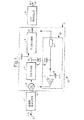
図1は、上記で参照した同時係属出願PCT/GB97/00405(公報番号WO97/30516)の図3に示される、DC除去回路、積分器及び比較器から構成される自己調整型遅延補償(SADC)回路について説明された原理に基づく位相雑音低減またはジッタ防止回路12を示す。
【0015】
入力波形またはパルス列Sが回路に供給される。Sは、発振器または周波数シンセサイザといった何らかの適切な周波数発生源によって発生され、電気または光ファイバ・ケーブルによって伝送されるかまたは電磁波によって伝送されるものであり、理想的または公称パルス繰返しまたは波動周波数fを有するが、また位相雑音(すなわち、等価的に、時間ジッタ)とパルスまたは波動の欠落の影響を受ける。
【0016】
入力によって高精度単安定回路1は同じ長さのパルスの列Mを出力する。このパルス列は、加算回路2で直流除去帰還回路10からの電圧をアナログ加算することで除去される直流(DC)成分を有する。次に反転積分器3が前記パルス列を鋸波形Nに変換し、それが基準レベルVrefと比較される。Vrefは有利には、積分器出力の平均直流レベルに近くなるよう選択される。比較器4からの出力Oは、立ち上がり端が規則的な間隔TOで発生するパルス列である。従って立ち上がり端は入力波形Sと比較してジッタを低減している。次に信号は出力(正エッジ・トリガ)単安定回路5に送られ、それによって出力パルス列Pが入力と同じ周波数fを有するが、立ち上がり端と立ち下がり端両方のジッタが低いことが確実になる。
【0017】
使用される構成要素の一部または全て(正エッジ・トリガ単安定回路、反転積分器、非反転比較器、非反転バッファ)の極性は、出力信号の極性と同様逆転できる。帰還ループを一巡する信号の最終極性反転が同じであるならば、追加の増幅器及び反転器を加えることも可能である。この種の変更は回路の概念を変えるものではない。
【0018】
直流除去回路10は抵抗8及びコンデンサ9を備える簡単な低域通過フィルタから成り、それにかかる電圧は高入力インピーダンスの非反転バッファ7を通じて加算回路2にフィードバックされる。回路ブロック11は、立ち上がり端ジッタ低減または位相雑音低減回路の役目を果たし、同時係属出願では自己調整遅延補償器すなわちSADCと呼ばれる。他の既知の直流除去回路が回路10の代わりに利用されることもある。
【0019】
単安定回路1のタイミング期間は有利には波形周期TOのごく一部分となるよう選択される。これによって高いレベルの雑音が抑圧される。単安定回路5のタイミング周期は、使用の際波形のマーク対スペース比が必要な周波数範囲にわたって1または無限大に近づかないように選択される。
【0020】
任意選択のツェナー・ダイオード6及び6’はパルスの損失なしに高速周波数スイッチングを提供する。積分器出力がツェナー・ダイオード電圧によって設定される上限または下限に達すると、これは入力周波数が十分に高くまたは低く急激に変化する時発生するが、ツェナー・ダイオードは有効に抵抗8をバイパスし、直接コンデンサ9に急速に電荷を供給する。これによってコンデンサ9で新しく必要とされる電圧ができる限り早く達成されるので、周波数の急激な変化の直後にジッタ消去が復元されるということを確実にする。この過程は、当業者にとっては明らかなように、例えばさらに別の比較器によるなど、他の回路の変形によって同様に行われることがある。
【0021】
この回路のジッタ低減動作が図2(a)から図2(d)に関して説明される。ジッタを伴い、1つのパルスが時間tjだけ間違えて配置された、入力単安定回路からの5つのパルスの列Mが図2(a)に示される。対応する積分器出力Nが、比較器出力O(図2(c))及び出力単安定回路5からの出力P(図2(d))と共に図2(b)に示される。
直流除去回路10によって、積分器3が飽和の方向にドリフトすることが防止される。直流除去回路のカットオフ周波数以下では、位相雑音は検出されないので消去できない。
【0022】
直流成分が正しく除去されるとすれば、回路の動作は次の通りである。図2(a)から図2(d)に見られるように、比較器4が積分器波形Nの正の勾配に切り換わる時間は、波形Mの中心パルスの時間ジッタtjに全く影響されない。波形Oのパルス正エッジが時間ジッタと無関係であることは、単安定回路Pからの出力波形にジッタがないことを意味する。回路は実際に、入力波形の時間ジッタと位相雑音を消去し、入力と同じ平均周波数のジッタのない波形を提供した。
【0023】
本発明の1つの態様による位相雑音低減またはジッタ防止回路32が図3に示される。2つの単安定回路19、19’が反転器18と共に使用され、システムが動作する周波数を2倍するならば、周波数トラッキングがより広範囲で低雑音な周波数2倍器33が得られる。
【0024】
この回路では、周波数fの入力パルス列または波形によって単安定回路19は各立ち上がり端で短パルスを出力する。反転器18の作用は、入力パルス列によって単安定回路19’が各立ち下がり端で短パルスを出力することである。ORゲート20によって、何れかの単安定回路19、19’からの短パルスS’が高精度単安定回路21に確実に伝送される。S’の公称周波数は入力の2倍、すなわち2fである。
【0025】
この周波数2倍器は、入力波形の「マーク」と「スペース」両方の期間が短パルス単安定回路のタイミング期間より長ければ動作する。
【0026】
次に単安定回路21は正確な長さの公称周波数2fのパルスの列M’を、図1に関してすでに説明した形式のSADC31に供給する。SADC31はその出力O’で立ち上がり端の時間ジッタを低減する。次にこの立ち上がり端を使用して2分周回路25を起動するが、その出力P’は入力の半分の周波数で、公称周波数fである。
【0027】
任意選択のツェナー・ダイオード26及び26’を回路31に追加することもでき、回路10で有するのと同じ利点を有する。
【0028】
図4(a)は、回路33で使用される短パルス単安定回路の有利な設計を図示する。この図を参照すると、単安定回路44は、立ち上がり端、さらには低速立ち上がり端の短反転パルスを提供する。これはフリップフロップ回路として交差接続された2つのNANDゲート41及び43を備え、ゲート42と出力反転器45を伴うが、その出力は、各立ち上がり端で、1つのNANDゲートによる信号伝播遅延の約3倍の長さの短時間のパルスからなる。提供されるパルスは必ずしも正確な長さではないが、短く、回路は集積回路の一部として容易に製造されるが、これは本発明による回路を実際に実現する際有益な特性である。
【0029】
図4(b)は、周波数2倍器入力回路33のために必要な2つの短パルス単安定回路19、19’、ORゲート20及び反転器18のための有利な設計を図示する。これは好都合にも8つのNANDゲートを使用している。NANDゲート46は反転器として使用される(代わりに反転器が使用されることもある)。NANDゲート47は、その入力が反転パルスであるため、各立ち上がり端または立ち下がり端について正パルスでORゲートの役目を果たす。
【0030】
利用形態によっては、図4(a)及び図4(b)のNANDゲートの内部及び/またはその間に負荷抵抗を追加することで、固定パルス長単安定回路として使用するのに十分なだけパルス長を一定にすることができる。
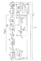
【0031】
図5は、それぞれ図1及び図3のジッタ防止回路12及び32と共通の機能を有し、実際に、その出力信号経路にジッタ防止回路を組み込んでいるクロック復元回路を図示する。
【0032】
この回路は顕著な周期性をもった電気信号波形またはパルス列をその入力として有するが、それでは個々の立ち上がり及び立ち下がり端は正確な時間間隔でなく、すなわち位相雑音の影響を受けており、また個々の波動またはパルス、または波動またはパルスの集合が完全に欠落していることがある。
【0033】
欠落パルス及び時間ジッタを伴う入力パルス列または波形S”はまず短パルス単安定回路50に供給され、そこで短パルス列に変換される。それらはORゲート51を介して高精度単安定回路52に供給され、そこで同一パルスの列M”に変換されるが、その直流レベルは回路53で直流除去回路67からの電圧をアナログ加算することで除去される。次にこのパルスの列は反転積分器54によって積分され、その出力N”は非反転比較器55と非反転比較器59の両方に供給される。比較器55は回路12及び32の場合と同様出力の立ち上がり端の時間ジッタを低減する効果を有する。同様に、抵抗61、バッファ60及びコンデンサ63は、回路12及び32の場合と同様信号M”の直流成分を減算する機能を有する。
【0034】
比較器59は、比較器55のトリガ・レベルVrefより高く設定されたトリガ・レベルVmpを有する。レベルVmpは、欠落入力パルスのない即ちパルス変換点をもった入力周波数源に対する回路の正常動作中に存在しうる積分器波形の最高レベルより高い。
【0035】
従って、比較器59は、入力パルス(または入力パルス列)が欠落している時だけ出力を発生する。次に比較器59によって、欠落パルスは短パルス単安定回路65によって、単安定回路50を通じて入力から到着するはずだったパルスの代わりにORゲート51に挿入される。
【0036】
この方法で、欠落パルスのタイミングに関して遅延された各再挿入パルスで出力パルス列が再構成される。この回路は、数個の入力パルスが欠けている場合パルスの長い列を挿入することができる。これが起こる時発生する波形が図6(a)から図6(d)に図示されている。
【0037】
最後に、上記で説明された回路12または回路32と同様の方法で構成された、任意選択のジッタ防止回路57が出力パルスの列に対して動作し、再挿入されたパルスの遅延による残留位相ジャンプを除去する。ジッタ防止回路57はまた、入力パルス列にすでに存在する位相ジッタも除去する。クロック復元回路が動作するシステムが、欠落パルスの再挿入またはすでに存在する何らかの位相雑音によって発生する位相ジャンプまたは時間シフトによって影響されない場合、ジッタ防止回路57は省略されることがある。
【0038】
入力パルスの長いシーケンスが欠落している場合、回路は直流除去回路の時定数を越えない時間だけ元の入力周波数で動作し続ける。この時間は、やはり図5に示される任意選択の回路構成によってかなり増大する。
【0039】
この任意選択の回路構成はスイッチ58とフリップフロップ・スイッチ制御回路64を備えている。スイッチ制御回路64はスイッチ58に接続されるが、これは高速FETスイッチまたは他の電子スイッチである。パルスが欠落している場合(積分器出力がVmpレベルより上昇すれば)、フリップフロップはスイッチの制御の役目を果たし、スイッチをオフに切り換えてコンデンサ63にかかる電圧を一定に保持する。スイッチ58が常時接続されたままになっていると、挿入された周波数は指数関数的な低下率でゆっくりと低下する。スイッチ制御回路64のリセットは入力単安定回路50のパルス出力から得られる。入力パルスが次に発生する時、スイッチ制御回路64はフィードバックを再接続する。
【0040】
挿入されたパルスの周波数のドリフトが特定の周波数Fpに向うことが望ましい状況があるが、これは任意選択の抵抗69及び電圧入力Vpの追加によって達成される。比較器55の出力インピーダンスが低いため、抵抗69を流れる電流は一般的には許容できる程度に低い。必要に応じて、スイッチ58は切り換えスイッチとなり、比較器55の出力と抵抗69の間で抵抗61の入力端を切り換える。
【0041】
68で示される回路ブロックは欠落パルス挿入回路を構成するが、これは他の回路でサブシステムとして使用されることがある。
【0042】
代替クロック復元回路86が図7に示される。回路32と同様、これは内部で周波数2fで動作する。前と同様、回路要素70、70’、71及び88からなる組合わせ体(assembly)73は回路33と同じ方法で周波数2倍器の役目を果たし、入力周波数fの2倍の信号を出力する。図5に関して説明されたパルス挿入回路68は出力に追加のパルス(単数または複数)を挿入する。次にこのパルスの立ち上がり端を使用して2分周回路76を起動するが、その出力P’は入力の周波数の半分、すなわち公称周波数fである。図5の回路66の場合と同様、回路86には必要に応じてジッタ防止回路87が含まれ、出力信号の時間ジッタを低減する。
【0043】
見られるように、それぞれ図5及び図7の回路66及び86は、入力周波数源が突然除去された場合、入力に存在する最後の周波数で動作または発振し続ける。
【0044】
さらに調べてみると、バッファ60の電圧が動作周波数を制御することがわかる。すなわち入力がない場合、バッファ60への入力信号が(おそらく電子スイッチまたは機械装置の何れかとのリンク62が切断された後で)出力周波数を制御する入力として使用される。この方法で、この回路は低い時間ジッタ(低位相雑音)電圧制御発振器として動作する。第2ジッタ防止回路57は任意選択であるが、できる限り低い位相雑音を達成することが望ましい。
【0045】
さらに、バッファ60の電圧が、実際の入力周波数の不適切な分数倍に等しい出力周波数を与えるよう事前設定されるか、それを与える方向にバイアスがかけられている場合、回路は非常に急速に「ロックオン」(lock on)する。不適切な分数とは、分子が分母より大きい2つの整数の比である。
【0046】
回路は入力周波数の選択された倍数に正確に位相同期しており、入力周波数が相当な範囲にわたって変化してもこの倍数に位相同期したままである。この方法で、クロック復元回路は汎用周波数逓倍器として動作する。この場合、第2ジッタ防止回路が使用され、パルス間隔を均等化し、実際の入力クロック・パルスの間に再挿入されたパルスについて発生する位相タイミングのジャンプを除去することがある。
【0047】
最後に、多周期性(multiple periodicities)の場合、回路が特定の周期性に対応する入力信号の選択されたスペクトル成分にロックオンするよう配置されることがある。これは、望ましい周期性のパルス列によって回路を事前調整することか、またはコンデンサ63にかかる電圧を事前設定することによって達成される。
【0048】
本発明の別の態様によれば、雑音低減回路は入力パルス列からスプリアス付加パルス、すなわち、公称入力周波数fのパルスに付加されたパルスを削除するのに有効である。前と同様、雑音低減回路にはジッタ防止回路が含まれ、パルス列中の時間ジッタを低減または除去することがある。ここで本発明のこの態様による雑音低減回路が、図8から図15に関して例として説明される。
【0049】
図8は、それぞれ図1及び図3に関して説明されたジッタ防止回路12及び32と共通の特徴を有するクロック復元回路119を図示する。回路119は時間ジッタを低減または除去し、また存在しうるスプリアス付加パルスを削除するのに有効である。
【0050】
入力パルス列または波形S*は時間ジッタの影響を受け、かつスプリアス付加パルスを含むことが想定される。
【0051】
入力パルス列または波形S*は初めANDゲート100、次に高精度単安定回路101に取り入れられ、そこで同一の長さのパルスの列M*に変換される。「高精度単安定回路」に対する技術的要求は厳密でないことが理解されるべきである。すなわち、高精度単安定回路からの出力パルスは単に繰り返し可能で、入力パルスの長さまたは隣接性とは無関係に同じであればよい。必要に応じて、短パルス単安定回路99が使用され定義済み論理パルスを提供するが、例えばそこでは入力パルス列は正弦波であるか、またはゆっくり立ち上がりまたは立ち下がりするアナログ信号である。高精度単安定回路101の立ち下がり端によって、ブランキング(blanking)単安定回路109は、高精度単安定回路101のパルス長さTpよりも短いパルス列または波形の公称時間周期Tに等しい時間周期Trより短い(しかし有利にはほぼ等しい)長さのパルスを発生する。またこれに代って、高精度単安定回路101の出力の立ち上がり端が使用され、それによってブランキング単安定回路109が、公称時間周期Tに等しい時間周期Trより短い(しかし有利にはほぼ等しい)長さTrのパルスを発生することもある。Trが最大値に近いほど、削除されるスプリアス・パルスが多くなる。しかし、許容される入力周波数の最大上向き変化はさらに小さくなる。
【0052】
パルス列B*中の各ブランキング単安定回路のパルスによって、ANDゲート100を使用する周期Trに関するさらなる入力パルスは禁止される。構成要素102、103、104、105、106、107及び108はジッタ防止回路(AJC)115を構成するが、その機能は前に説明されている。ジッタ防止回路115の効果はパルス列M*からジッタを除去することである。
【0053】
単安定回路109とANDゲート100は入力パルス列からスプリアス付加の後パルス、すなわち入力パルス列中の予想されるパルスの後に発生するパルスを除去する。この後パルスはパルス列の劣化なしに除去される。しかし、スプリアス付加の前パルス(すなわち、予想されるパルスの前に発生するパルス)は予想されるパルスの除去に帰結する。この場合、結果として生じるパルス列M*はその正しい位置より前の位置にジッタしているパルスを含む。しかし、AJC115はこのジッタを除去するので、パルス列M*は規則的なパルス列P*に復元される。
【0054】
図9は、やはりスプリアス付加パルスを削除しジッタ防止効果を有するのに有効な代替回路131を図示する。回路131では、入力パルスS*’はまず必要に応じて短パルス単安定回路120により短パルスに変換された後、ANDゲート121を通じて高精度単安定回路122に与えられる。構成要素122から124はジッタ防止回路として機能する。
【0055】
しかし、この回路では積分器124の出力は二重の機能を有する。すなわちそれは、ANDゲート121を通じて余分のパルスを削除するブランキング・パルスB*’を生成するために使用される非反転ブランキング比較器130を制御する。生成されたブランキング・パルスB*’は高い方の周波数の入力パルス列S*’よりも短く、低い方の周波数の入力パルス列S*’よりも長い。パルス列B*’のデューティサイクルは、比較器130に印加される電圧VBによって選択される。前と同様、ジッタ防止回路要素は、すでに入力パルス列中に存在し、かつパルス削除の結果生成されるジッタを除去する役目を果たす。
【0056】
回路131は回路119に対して、より広い入力周波数範囲にわたり、より高いジッタ値を有する入力パルス列S*’を処理できるという利点を有する。
【0057】
図10(a)から図10(d)は、回路119の様々な点で見られる波形を示す。説明される例では、波形S*(図10(a))は、ジッタしている(前にずれた)パルスP2と、付加スプリアス・パルスP3’(後パルス)を含んでいる。積分器出力波形N*(図10(b))が、出力P*(図10(c))及びブランキング・パルス列B*(図10(d))と共に示される。代替回路131で見られる波形は、ブランキング・パルスが可変長である以外は同様である(これは図12(a)から図12(d)で見られる)。
【0058】
図11は、周波数2倍器入力を有するジッタ防止及びスプリアスパルス削除回路150を示す。周波数2倍器入力は短パルス単安定回路140及び141、反転器142及びORゲート143を備えている。回路131に基づくジッタ防止及びパルス削除回路144がパルス列を処理するために使用され、その出力が2分周回路145に供給されて入力パルス列S*と同じ公称周波数を有する出力パルス列を生成する。回路の代表的な波形が図12(a)から図12(d)で示される。パルス列S*”は1:1に等しくないマーク対スペース比を有するが、これは回路144への入力でL*”のようなパルス列を発生するため、119で参照される種類の回路にとって問題である。しかし、131で参照される種類の回路はこの種のパルス列を扱うことができるが、これはブランキング比較器が積分器出力N*”から、波形の長い間隔中には長いブランキング・パルスを有し、短い間隔中には短いブランキング・パルスを有するブランキング波形B*”を発生するからである。
【0059】
図13は、「終了」入力を有する特殊ラッチ回路156を示す。回路156は、それぞれ図8及び図9に示される加算ANDゲート100及び121の代替として使用される。回路156は図4(a)に関して説明された回路44と同様であり、必要に応じて、それぞれ図8及び図9に関して説明された短パルス単安定回路99及び120の機能に取って代る。短パルス単安定回路の機能を有するこの種の回路は、英国特許第1462408号で説明されている。
【0060】
回路156にはNANDゲート150、151及び152と反転器153が含まれる。正入力信号パルスは、出力が論理ロー(low)になる時、終了信号が戻って受信されるまで出力に伝送される。回路156は負論理終了信号、すなわち、通常は論理1であり、0への変換点で出力パルスを終了する信号を有する。
【0061】
回路119及び131の場合、短パルス単安定回路99及び120とANDゲート100及び121は説明された種類のラッチ回路によって置き換えられ、ブランキング・パルスB*、B*’は反転器を通じて終了入力に供給される。回路150の場合、各短パルス単安定回路140、141はそれぞれラッチ回路156によって置き換えられ、禁止パルス列が反転器を通じてラッチ回路の終了入力に供給される。図14は、図9に関して前に説明された回路131に応用された回路156を示す。ラッチ回路191は回路156と同じ回路で、図9に示される短パルス単安定回路120及びANDゲート121に取って代るが、一方他の構成要素192から200は構成要素122から130と同じ機能を有する。
【0062】
図15は、ジッタ防止、スプリアス・パルス削除及び欠落パルス挿入機能を有するクロック復元回路180を示す。ORゲート163は、任意選択の単安定回路161からの入力パルスと単安定回路162からの挿入パルスを取り入れる。これらのパルスの一部はANDゲート164を介してブランキング比較器173からのパルス列によって禁止される。高精度単安定回路168は一定の長さのパルスを発生する。単安定回路165は、加算回路166、反転積分器167、比較器168、増幅器170、抵抗171、コンデンサ172及び出力単安定回路169と共にジッタ防止回路を構成する。パルス挿入の機能性(functionality)は、基準電圧Vmpと積分器出力を入力とする非反転比較器174によって提供される。比較器174の出力は、必要な場合短パルス単安定回路162によって加算される挿入パルスになる。パルス削除機能は、基準電圧VBと積分器出力を入力とする非反転比較器173によって提供される。比較器174の出力は、ANDゲート164によって削除されるスプリアス付加パルスになる。
【0063】
回路180は必要に応じて、それぞれ図3及び図11に関して説明された回路32及び150で使用される周波数2倍器入力回路を装備する。
【0064】
別の実施例では、説明された種類の2つのパルス削除回路が使用される。1つは入力波形に対して作用し、もう1つは入力波形の極性反転に対して作用する。パルス削除回路からの出力パルス列は異なった2分周回路に供給され、それらの出力はORゲートで結合され1つの共通出力を形成する。また、パルス削除回路からの出力パルス列がフリップフロップ回路の入力をセット及びリセットするために供給され、フリップフロップ回路の出力が1つの共通出力を形成することもある。
【0065】
回路180には必要に応じて、図5に関して説明されたパルス挿入回路66で使用されるような多数のパルスを挿入する構成要素が含まれる。スイッチ制御フリップフロップ64、スイッチ58及び追加抵抗69を含むこうした構成要素は、明瞭にするため図15から省略されている。
回路119、131、150及び180は適度に小さいジッタの出力を達成する。大きなジッタ値を誘発する挿入及び削除されたパルスは復元され、挿入または削除されたパルスのずれによるジッタは本質的に低減される。しかし、追加のジッタ防止回路が必要に応じて回路119、131、150及び180の何れかの出力線に追加され、さらに出力パルス列のジッタ値を低減することがあるが、これは、例として、図14の202で示されている。
【0066】
ここで説明された全ての回路では、変更が電子回路の当業者にとっては明らかであるが、これは本発明から大きく変化するものではない。例えば、論理ゲートの集合が、本発明と同じ数学関数(ブール論理関数)を有する代替集合によって置き換えられることがある。
【0067】
回路119、131、150、180及び201は、雑音、干渉、クロストークまたはスプリアス付加パルスを発生する他の問題及び発生するジッタの影響を受ける通信回路のクロック信号及び他の規則的パルス列の復元に応用される。
【0068】
クロック信号を伴う応用例では、一定の公称周波数を有していても、入力パルス列に対して調整可能な位相及び/またはマーク対スペース比を有する単一クロック信号を提供する必要がある。別の応用例では、同じ公称周波数を有するが、お互いに及び/または入力パルス列に対して異なった位相及び/またはマーク対スペース比を有する2つかそれ以上のクロック信号を提供する必要がある。本発明の別の態様は、例えば多位相、多出力クロック分配回路といった応用例で使用される雑音低減回路を提供する。
【0069】
図16は、単一クロック信号を発生する位相雑音低減回路を図示する。この回路は二重比較器セット/リセット・ラッチ出力部を使用する。
【0070】
図17(a)から図17(e)は、図16の回路の様々な点で観察される電圧波形を図示する。
【0071】
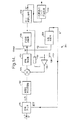
図16を参照すると、パルス列S1が単安定回路301への入力であり、そこでS1は各々同じ長さのパルスS1’の列に変換される(入力パルス列がすでに同一の長さのパルスを有している場合、単安定回路301は省略できる)。次にパルス列S1’は、S1’の直流成分を減算する働きをする加算回路302を通じて反転積分器303に供給される。積分器303の出力Iは2つの比較器307及び309に供給される。比較器307は、抵抗304、コンデンサ305、増幅器306及び加算回路302を備える直流レベル減算回路に給電する。
【0072】
比較器307及び309はまた、比較信号C1及びC2をそれぞれ単パルス単安定回路308及び310に供給する。C1及びC2の各立ち上がり端で、短反転パルスが発生するが、、これは交差接続されたNANDゲート311及び312を備えるセット−リセット・ラッチ313をそれぞれ設定(C1)またはリセット(C2)する。短パルス単安定回路は従来の集積回路単安定回路ブロックであるか、または代替的に英国特許第1462408号で説明された形式である。場合によっては、短パルス単安定回路308、310は簡単な交流結合コンデンサによって置き換えられることがある。
【0073】
入力周波数の変化に対する回路の応答を高速化するために、図1及び図3に関して説明されたような高速化回路が使用されることがある。これは、積分器303の出力から直流レベル減算回路の入力抵抗304に接続された2つの直列背中合わせに接続されたツェナー・ダイオードを備えている。構成要素301、302、303、304、305、306及び307のジッタ防止作用の結果、C1及びC2の立ち上がり端はどちらもジッタがないので、出力信号Oは立ち上がり及び立ち下がり端の両方でジッタがない。
【0074】
入力パルス列S1と出力パルス列Oの間のデューティサイクルと位相関係は、それぞれ比較器307、309に印加される電圧Vref1及びVref2によって選択される。
【0075】
説明された回路配置は、立ち上がり及び立ち下がり端の両方でジッタが低減されるという利点を有する。これは、入力の周波数2倍器と出力の2分周回路の必要なしに、より広範な入力周波数範囲の入力パルス列を扱うことができるという利点を有する。これは、積分器303によって出力される鋸波形の振幅が低い方の周波数で低減するため、周波数が低下するに連れて比較器のトリガ時間間の間隔が増大するという付加的な利点を有する。すなわち、周波数が変化してもマーク対スペース比は少なくともほぼ一定である。
【0076】
図18は、多位相出力、例えば多位相クロック信号を発生することのできるジッタ防止回路を示す。構成要素321、322、323、324、325、326、327は、入力信号からのジッタのない立ち上がり端を提供するジッタ防止回路を形成する。比較器327及び329は短パルス単安定回路328及び330に給電し、ラッチ333をセット及びリセットするが、ラッチ333の出力O1は、図16の場合と同様、回路の第1出力である。1つかそれ以上の追加回路の追加によって1つかそれ以上の追加出力が提供されるが、355で示されるその1つだけが図示される。回路355は比較器347、349、短パルス単安定回路348、350及び出力ラッチ353を含む。比較器への入力基準電圧を選択することによって、回路または各回路355の出力はデューティサイクル及び相対位相に関して制御される。応用例によっては、相対位相を制御できる一方で、多位相クロック生成器の全ての出力から標準長さのパルスを提供することが好都合である。この可能性は、供給される制御電圧V2に基づいて、2つの間の一定の電圧差を維持する任意選択のダイオード351及び352と任意選択の抵抗354といった回路によって、基準電圧を比較器の対に供給することで簡単に提供される。図18に関して説明された回路は、広範な入力周波数にわたって動作できる点で有利である。
【0077】
狭い範囲の入力周波数でジッタ防止回路に基づく多位相クロック生成器において同様の長さのクロック・パルスを達成する別の方法が図19に示される。構成要素361、362、363、364、365、366及び367は、ツェナー・ダイオード368及び369を備える高速化回路を組み込んだジッタ防止回路を備えている。この回路にはまた、単安定回路370と多数の比較器/単安定回路の対が含まれる。この実施例には、371と372、373と374、375と376で示される3つのこうした対が存在する。図20(a)から図20(f)は、図19の回路の様々な点で観察される電圧波形を示す。図16、図18及び図19に示される回路と同様の回路が、図1から図7に関して説明された種類のパルス挿入回路及び/または図8から図15に関して説明された種類のパルス削除回路を備えることがあり、こうした回路はクロック信号の復元に有益である。
【0078】
本発明のこの態様によって説明されたジッタ防止回路は、T.V.Rama Murthyによる論文「方形波用連続移相器」、電子工学、1979年4月中旬、19ページで説明されている種類の多位相出力回路構成に適しており、入力との任意位相関係を提供する。この論文で説明されている回路構成は方形波に関するが、この回路構成はより一般的な形で比較器にしきい値を提供することで、明らかに任意のマーク対スペース比及び位相関係の出力波形に適応可能である。
【0079】
本発明の別の態様は、低雑音フラクショナルレート乗算回路、特に、排他的ではないが、フラクショナルN位相同期ループ・シンセサイザで有益な低雑音フラクショナルレート乗算回路に関する。
【0080】
電子工学では、一定の基準周期信号源の倍数または分数である周波数の新しい周期的電気信号源を生成することが必要であることが多い。新しい信号はジッタを有する。すなわち、その信号端(signal edge)は同じ周波数の正確な周期信号の信号端に対して変化する。このジッタを低減することが本発明のこの態様の目的である。以下の説明では、位相雑音がジッタと呼ばれる。位相雑音はジッタに比例するので、一方の低減はもう一方の低減と同等である。
【0081】
以下の実施例では、使用されるジッタ防止回路(AJC)は、添付の図面の図1から図3に関して説明された回路のような、WO97/30516で説明されている種類のものである。
【0082】
1つのAJCを使用する代わりに、1つのAJCの出力が別のAJCの出力になるように相互接続された2つかそれ以上のAJCの一連の縦続を使用することも代替的に可能である。第1AJCによってなされたジッタ低減が次のAJCによって増大され、以下それが続く。例えば、1つのAJCが20dBのジッタ低減を有するならば、理想的には2つのそのようなAJC回路の縦続は40dBのジッタ低減を有し、理想的には3つのAJCの縦続は60dBのジッタ低減を有する。実際には、この過程はAJC構成要素の雑音性能によって制限されるので、ジッタ低減は2より多い各回路について著しく低下する。従って、3より多いAJC回路を縦続で利用する価値はほとんどない。
【0083】
比較的簡単な応用例では、高速基準源が発生源として使用され、そこから望ましい低周波数が得られる。
【0084】
周波数合成でAJCを使用する最も簡単な方法は、高周波数源に応用されるモジュールN分周器(module−N divider)に1を加算することである。モジュールN分周器は、正確に分周比N(modulus of division N)によって、出力波形の周期に対するジッタを低減する。しかし、残留ジッタはAJCの使用によってさらに低減できる。AJCが十分に高い動作周波数で得られるならば、AJCは直接高周波(HF)基準に応用される。そうでない場合、AJCは初期分周段Niの後で応用され、AJCの後さらにNoによって分周されるが、ここでNi・No=Nである。
【0085】
AJC回路は、ある種のレート乗算回路と共に直接使用される場合より大きな影響を有する。フラクショナルレート乗算回路の機能は、Aが例えば1から1000まで変化し、Bが1000で一定である時、B個の入力パルス毎にA個のパルスを出力するというものである。すなわち、入力周波数はA/Bによって乗算される。フラクショナルレート乗算器はいくつかの設計が可能であるが、それらは出力が有する固有のジッタの量によって異なる。
【0086】
レート乗算器の特に好都合な形式は、一定の数である位相増分を累算器に逐次加算し、累算器がオーバフローする毎に出力を与える種類(逐次加算レート乗算器すなわちSARM)のものである。これは、最大出力ジッタが出力波形の1つの全周期より小さくなるように入力パルス列中のパルスをスキップすることで動作するという利点を有する。この種の波形はAJCによって正しくジッタ除去されるので、SARMはAJCの追加によって簡単に強化される。(1ビット出力を有する直接デジタル周波数シンセサイザ(DDS)はSARMと同等であることに注意のこと)。図25は、1つのAJC回路またはさらに良好な直列の2つのAJC回路が10MHz信号中のスプリアス500kHz成分をどのように低減できるかを示す。
【0087】
BCDレート乗算器HEF4527形(「HE4000B論理素子ファミリーCMOSハンドブック」を参照のこと、Philips Semiconductor PO Box 218、5600 MD Eindhoven)のような簡単なレート乗算器は7/10による乗算で高い固有の出力ジッタを有する。例えば、HEF4527は、単位間隔当たり4パルス、次に欠落パルスのギャップ、次に単位間隔当たり3パルス、次に二重の欠落パルスのギャップ、すなわち、1つの出力周期全体を越える最大出力ジッタを与える。こうした波形(及び縦続HEF4527回路からの同様の波形)はジッタが多すぎて、直接AJCによってはうまくジッタ除去できない。その代わり、AJCが応用される前に、フラクショナルレート乗算器の後に分周器がなければならない。一般的なBCD乗算器の場合、必要な分周器は、2以上のどのような整数の分周比でも有することができる。2分周出力周波数が許容できない場合、出力はある範囲の既知の乗算回路、例えば二倍高調波乗算器を使用して2倍することができる。
【0088】
大きな数の可能な分周比を効率的に提供するために、分周器とAJCを使用するさらに高度な方法、例えばパルス減算を含むものが有益である。
【0089】
図21を参照すると、パルス減算器401は入力パルス列S2から孤立パルスを除去し、修正パルス列S2’を発生する。ジッタ防止回路402(AJC)は信号上のジッタを低減し、パルス列O2またはO2’を低減する。AJC402が出力単安定回路を有さない場合、パルス端の一方だけでジッタが低減された波形O2が見られる。出力単安定回路がある場合、出力パルスの両端が低いジッタを有する波形O2’が見られる。プログラム可能分周器403が周波数を整数因数Naで分周した後、プログラム可能分周器404は周波数をさらに別の因数Na’で分周する。フラクショナルレート乗算器405は、M個の入力パルスを受信する毎にAa個のパルスを出力する。図21の回路は、入力周波数に全て正確に関連する非常に大きな数の可能な出力周波数を発生する汎用性のある方法を提供する。動作周波数に関する時定数とAJC402内部の時定数の後に、出力信号は入力信号に位相同期される。任意選択のN分周回路406が示されるが、これによってAJC402は欠落パルスをより容易に処理できる。最良の総合ジッタ低減を得るにはNは小さくすべきであるが1にすべきではない。応用例によって、波形O2、O2’、D、D’が出力として使用される。
【0090】
図22(a)から図22(e)は、AJCが使用されレート乗算器の出力中のジッタを抑圧する図21の回路の様々な点で観察される一般的な波形を示す。図22の囲みは、レート乗算器が入力パルスS2の5つ毎に1を減算してジッタ付き波形S2’を生成する1つのサイクル全体を示す。AJC402内部の積分器の波形がトレース(trace)I(図22(c))として示される。
【0091】
回路の動作を説明するため、1つの例が検討される。入力パルス列S2が100MHzの入力周波数を有し、Naが100に設定され、Aaが100に設定され、Na’が1に設定される(分周器404を省略し直接接続に置き換えることと同等)と仮定される。出力パルス列O2/O2’はパルス減算の前にf/100=1000kHzの基本周波数を有する。フラクショナルレート乗算器は100の入力毎に50パルスを出力する、すなわち、500kHzのレートでの入力パルスの減算である。この減算されたパルスによってAJC402への入力は99.50MHzに低下する。これはフラクショナルレート乗算器の出力を大きくは変化させないので、O2の出力周波数はほぼ正確に99.5MHzであり、波形Dの分周された出力周波数は99.5/Na’、すなわち995kHzである。実際には、レート乗算器に入力されるパルスの減少数を考慮した出力周波数を求める正確な公式は、
Fo=Fi/(Na+Aa)
であるが、ここでFi及びFoはそれぞれ入力及び出力周波数である。これによって、上記で引用された例について、995.025kHzの分周された出力周波数が得られる。
【0092】
明らかに、この例では、Na及びAaの設定によって10,000の個別の周波数の選択が可能である。これらは、入力周波数が100MHzである図21による回路を使用しての可能性である。Aaは0.01単位の0.01から0.99まで可変であり、Naは201から1まで可変である。選択可能な周波数はスペクトル全体に均一に広がっており、間隔は出力周波数の割合で、500kHz出力での0.005%から最悪の場合(100MHz近く)の1%まで増大する。
【0093】
こうした設定は、分周器403を(例えば)1と1000の間の値に設定することに結び付けられ、100MHzから100kHzまでほぼ連続的な範囲の出力周波数O2/O2’が与えられるので、この例では、0.1Hzから100Hzのステップで、100kHzから100MHzの周波数が利用可能である。下流の分周器404の使用によってさらに低い範囲の周波数にアクセスできる。
【0094】
図23に示される本発明の代替実施例は、パルス減算器401の代わりにパルス挿入器411を使用する。それ以外の点では、この回路は図21に関して説明されたものと全く同様の方法で機能する。
【0095】
利用可能な基準周波数を、おそらくは大きく越える出力周波数が必要な場合、例えば、「無線受信機」W Gosling (編)、Peter Peregrinus Ltd、1996年、第4章「周波数シンセサイザと標準」M Underhill、ISBN−0−86341056で説明されているような位相同期ループ(PLL)概念が使用される。この概念を使用すると、出力を提供する電圧制御発振器は基準周波数の正確な倍数(おそらくは分数倍)に位相同期される。PLL回路でAJC回路を使用することで、通常のジッタ性能劣化なしにフラクショナルN合成が可能になる。
【0096】
図24を参照すると、サブシステムとして図21及び図23の回路によって例示された種類の低雑音フラクショナルレート乗算器440を組み込んだフラクショナルN周波数シンセサイザが示される。この回路は電圧制御発振器(VCO)433を基準発振器430の高調波または分数調波に位相同期する。VCO433を、それぞれ分周器434、436及びプリスケーラ438の設定N、N’及びN”によって制御される非常に大きな数の可能な個別の周波数に位相同期することができる。
【0097】
N、N’及びN”の選択は次のように決定される。
【0098】
N”は理想的には1(すなわち、プリスケーラなし)であるが、非常に高い周波数のVCOの場合、最高限度のVCO周波数でプログラム可能分周器を動作させることができないことがある(プログラム可能分周器の多くは簡単なプリスケーラ・フリップフロップによる回路より3倍以上低速で動作する)。この場合、おそらく2または4または8である小さい因数N”を使用すれば通常十分である。プリスケーラ用に使用される高速論理素子の電力消費が大きいため、このアプローチはシンセサイザ・システム全体の電力消費を最小化するためにも使用される。N’はやはり理想的には1(すなわちAJD435の前の分周器なし)である。しかし、AJC435は複雑で、一般に高速VCOと同じ速さで動作することはできない。また、AJCはパルス周波数が低いほど良好なジッタ低減を提供する。N’は、AJCがそのジッタ低減を大きく劣化させることなく動作できる周波数を最大化するよう選択される。Nは、基準周波数よりわずかに大きい出力周波数を与える最も近いモジュールN分周を提供するよう選択される。これによってフラクショナルレート乗算器によって減算されるパルスが最小となり、ジッタの発生が最小化される。
【0099】
プログラム可能分周器は有利には、Philips HEF4751及びSAA1057周波数シンセサイザ集積回路によって例示される多重帰還形のものである。
【0100】
フラクショナルレート乗算器の係数Aは、VCOを必要な出力周波数に同調した後位相同期できる周波数でパルスを減算する(位相比較器に与えられる比較周波数を低下させる)よう選択される。
【0101】
例えば100kHzの基準発振器と100MHz〜1GHzを発生できるVCOの場合、分周器N、N’及びN”は1000〜10,000の分周比を達成するよう設定する必要がある。N”が1であると仮定し、N’=10及びN=500とする。この方法で、回路位相比較器は電圧をVCOに伝え、VCOは500MHzまで上昇する。フラクショナルレート乗算器が1000番目毎のパルスを減算するよう設定されると仮定する(0.999のレート乗算A)。この方法で1000パルス毎、すなわち10ミリ秒ごとに、パルスは発振器出力から除去される。これによって分周器への入力の周波数は、10ミリ秒毎に1パルス、すなわち500.000000MHzから499.999900MHzに低下する。この低い周波数の入力は位相比較器で見られ、そこから増大した電圧がVCOに伝えられ、そこで周波数は、わずかなシステム時定数の経過後500.000000MHzから500.000010MHzに上昇する。N(及びN’、N”)及びAの適切な選択によって、VCOを100MHzから1GHzまでの9百万の周波数の何れか1つに位相同期できることを示すのは容易である。
【0102】
本発明のこの態様によって構成されたAJCを伴うフラクショナルNシンセサイザは性能の改善が達成可能であることを示した。この例では、Motorolaの集積回路MC12022A 64/65形プリスケーラが利用され、パルス減算を提供した。2つのBVDレート乗算器、CD4522B形回路が縦続にされ、6.991kHzの基準周波数で1/100のステップを提供した。プログラム可能分周器はMotorolaのMC14060B形回路であり、位相比較器はMotorolaのMC14046B形回路であった。ループ・フィルタは製造業者のデータ・シートの情報によって設計されたが、積分器コンデンサの大きさは、比例ループ利得を同じに保つため増大された。その結果、ループフィルタは、初期位相同期が達成された後タイプ1システム・ループフィルタであるかのように動作する。使用されるVCOはMotorolaのMC1648形回路であり、出力周波数は115MHzであった。
図26は、本発明によるフラクショナルN周波数シンセサイザの出力中の(a)6.991kHz及び(b)139.82Hz成分のAJCによるジッタの抑圧効果を示す。基準及びその高調波スプリアス信号は、分周器チェーン(chain)のAJCによって大きく抑圧される。6.991kHz間隔の成分における19dBの低減は思いがけないほど大きかった。139.82Hz間隔の成分における10dBの低減は、この実証で実際に利用された種類のパルス幅型よりむしろサンプル/ホールドまたは高利得位相比較器の使用によって改善されているだろう(位相比較器の性能劣化が、AJCによって達成されたジッタの改善を隠している)。
【0103】
一般に、図21、図23及び図24の回路で使用されるパルス減算器及びパルス挿入器は入力パルス列の固有ジッタを増大する。同様に、フラクショナルレート乗算器は実際上そこに入力されるパルスを削除するが、これもジッタを発生する。しかし、これらの回路で使用されるAJC回路は、このジッタの追加発生源(固有のジッタと同様)を20dB以上低減することができる。ジッタはさらにこのシステムで、Nの係数だけ、すなわちプログラム可能分周器の比で低減される。
【0104】
説明されたパルス減算器は可変分周比分周器(variable modulus dirider)と計数器を含む回路によって置き換えられる。例として、公称分周比が10である分周器を、制御信号に応答して110の連続入力パルスの与えられた集合について11の係数で分周するよう切り換えることができる。すなわち、110のパルスに対して11でなく10のパルスが出力される。さらに簡単な回路でも1または2の何れかで分周するよう切り換えることができる。回路が2で分周を行うよう指令される度毎に、それは有効に入力パルスの1つを除去する。
【0105】
同様に、説明されたパルス挿入器も、可変分周比分周器と計数器を含む回路によって置き換えられる。例えば、10の公称分周比を有する分周器を、90の連続入力パルスの与えられた集合について9で分周するよう切り換えることができる。すなわち、90のパルスに対して9でなく10のパルスが出力される。
【0106】
ここで説明された全ての回路では、変更が電子回路の当業者に明らかであるが、これは本発明から大きく変るものではない。例えば、論理ゲートの集合が、同じ数学関数(ブール論理関数)を有する代替集合によって置き換えられることがある。
【0107】
すでに説明されたように、本発明による回路は、特に、雑音、干渉、クロストークまたはジッタを発生させる他の問題の影響を受ける通信回路のクロック信号及び他の規則的パルス列の復元に応用される。
【図面の簡単な説明】
【図1】 図1は、公知の位相雑音低減回路を示す図である。
【図2】 図2(a)から図2(d)は、図1の位相雑音低減回路の動作を理解する際に有益な様々な波形を示す図である。
【図3】 図3は、本発明による位相雑音低減回路を示す図である。
【図4】 図4(a)と図4(b)は、図3の位相雑音低減回路で使用される短パルス単安定回路を示す図である。
【図5】 図5は、本発明によるクロック復元回路を示す図である。
【図6】 図6(a)から図6(d)は、図5のクロック復元回路の動作を理解する際に有益な様々な波形を示す図である。
【図7】 図7は、本発明による別のクロック復元回路を示す図である。
【図8】 図8は、本発明によるクロック復元回路を示す図である。
【図9】 図9は、本発明による代替クロック復元回路を示す図である。
【図10】 図10(a)から図10(d)は、図9の回路の様々な点で観察される電圧波形を示す図である。
【図11】 図11は、周波数2倍入力を有するジッタ防止及びスプリアス・パルス削除回路を示す図である。
【図12】 図12(a)から図12(d)は、図11の回路の様々な点で観察される電圧波形を示す図である。
【図13】 図13は、ラッチ回路を示す図である。
【図14】 図14は、図13のラッチ回路を組み込んだクロック復元回路を示す図である。
【図15】 図15は、別のクロック復元回路を示す図である。
【図16】 図16は、本発明による位相雑音低減回路を示す図である。
【図17】 図17(a)から図17(e)は、図16の回路の様々な点で観察される電圧波形を示す図である。
【図18】 図18は、代替位相雑音低減回路を示す図である。
【図19】 図19は、代替位相雑音低減回路を示す図である。
【図20】 図20(a)から図20(f)は、図19の回路の様々な点で観察される電圧波形を示す図である。
【図21】 図21は、本発明によるフラクショナルレート乗算回路を示す図である。
【図22】 図22(a)と図22(b)は、図21の回路の様々な点で観察される電圧波形を示す図である。
【図23】 図23は、本発明による代替フラクショナルレート乗算回路を示す図である。
【図24】 図24は、図21または図23のフラクショナルレート乗算回路を含むフラクショナルN周波数シンセサイザを示す図である。
【図25】 図25(a)、図25(b)及び図25(c)は、それぞれAJCなし、1つのAJC及び、縦続接続された2つのAJCの場合発生する、10.1MHzで動作する1ビットDDSの出力の周波数スペクトルを示す図である。
【図26】 図26(a)及び図26(b)は、本発明によるフラクショナルN周波数シンセサイザの出力のそれぞれ6.991kHz成分と139.82Hz成分のAJCによる抑圧の効果を示す図である。[0001]
The present invention relates to a noise reduction circuit which is a noise reduction circuit useful for a clock recovery circuit, for example.
[0002]
The present invention is also particularly applied in fractional rate multiplier circuits and fractional-N frequency synthesizers.
[0003]
Computational and telecommunications systems operate with internal or external clock signals that provide modulation, demodulation, analog-to-digital conversion and data stream synchronization. System clocks often require a high level of purity and / or integrity. Purity means low phase noise that is directly proportional to time jitter. Phase noise or time jitter occurs when the position of the pulse in the pulse train deviates in time from the position expected based on the strict periodicity assumption of the pulse train. The term “identity” refers to a pulse stream that has no missing operation conversion points and no spurious additional conversion points.
[0004]
A known phase noise reduction or jitter prevention circuit is described in PCT / GB97 / 00405 (publication number WO97 / 30516). This circuit produces an output that has the same frequency as the input, but with reduced output pulse jitter compared to the input pulse.
[0005]
The noise reduction circuit according to the present invention is used to reduce noise caused by low levels of purity and / or identity. The circuit according to the present invention is applied in various ranges, for example, as a clock recovery circuit in a multiphase output clock distribution circuit, a low noise fractional rate multiplication circuit, and a fractional N phase locked loop synthesizer.
[0006]
According to a first aspect of the present invention, there is provided a noise reduction circuit for reducing noise in an input pulse train consisting of pulses that are periodic in the absence of noise and missing one or more pulses, The noise reduction circuit includes a direct current removing means for removing a direct current level from the input pulse train, an integrating means for integrating the input pulse train after the direct current level is removed by the direct current removing means, an output from the integrating means for receiving the input pulse train A detecting means for detecting a missing pulse therein, a pulse generating means for inserting an additional pulse delayed with reference to the missing pulse detected by the detecting means in response to the detecting means, and the integration Output means for obtaining an output pulse train from the output from the means.
[0007]
According to a second aspect of the present invention, a voltage source for generating a presettable voltage, an integrating means having an input for receiving the presettable voltage, and an input to the input in response to an output from the integrating means. There is provided a voltage controlled oscillator comprising means for providing a pulse and means for obtaining a periodic pulse train of a frequency determined by a presettable voltage from the output.
[0008]
According to a third aspect of the present invention, an integrating means having an input for receiving an input pulse train having a nominal frequency f, a voltage source for supplying a presettable voltage to the input, and an output from the integrating means Means for responsively inserting additional pulses into the input pulse train; and means for obtaining a periodic pulse train of frequency nf from the output when n is a multiple greater than 1 determined by the presettable voltage. A frequency multiplier is provided.
[0009]
According to a fourth aspect of the present invention, there is provided a phase noise reduction circuit for reducing phase noise in an input pulse train consisting of pulses having a nominal frequency f when there is no phase noise. Means for obtaining a first pulse train from an input pulse train, wherein the first pulse train comprises a pulse triggered by a positive direction conversion point of a pulse forming the input pulse train, and means for obtaining a second pulse train from the input pulse train. Means comprising a pulse triggered by a negative direction conversion point of a pulse forming the input pulse train, a coupling means for coupling the first and second pulse trains to form a combined pulse train, DC removal means for removing the DC level for the pulse train, and after the DC level is removed by the DC removal means to generate an integral output It comprises an integration means for integrating a slip pulse train, and processing means to obtain an output pulse train of the nominal frequency f from the integrated output.
[0010]
According to a fifth aspect of the present invention, there is provided a circuit for reducing noise in an input pulse train consisting of a plurality of pulses that are periodic in the absence of noise and have one or more spurious additional pulses therein. This circuit includes a direct current removing means for removing a direct current level from an input pulse train, an integrating means for integrating the input pulse train after the direct current level is removed by the direct current removing means, and a pulse removal for removing the spurious added pulse from the input pulse train. Means and output means for obtaining an output pulse train from the output of the integrating means.
[0011]
According to a sixth aspect of the present invention, there is provided a circuit for reducing phase noise of an input pulse train consisting of a plurality of periodic pulses in the absence of noise, the circuit removing a DC level from the input pulse train. A direct current removing means, an integrating means for integrating the input pulse train after the direct current level is removed by the direct current removing means, and generating different output pulse trains in response to reference signals different from the outputs of the integrating means, respectively. Each of the output pulse trains includes at least two detection means including periodic conversion points having a phase relationship with the input pulse train depending on the corresponding reference signal.
[0012]
According to the seventh aspect of the present invention, the pulse train correcting means for subtracting the pulse from the input pulse train in response to the control pulse or adding the pulse thereto in response to the control pulse to generate the corrected pulse train; Frequency dividing means for dividing, a fractional rate multiplier for obtaining a control pulse from the divider output and supplying the control pulse to the pulse train correcting means, and jitter for reducing the jitter of the corrected pulse train before frequency division by the frequency dividing means And a fractional rate multiplication circuit comprising a reduction means.
[0013]
According to an eighth aspect of the present invention there is provided a fractional N frequency synthesizer comprising a phase locked loop including a fractional rate multiplier circuit according to the seventh aspect of the present invention.
[0014]
Embodiments of the present invention will now be described by way of example only with reference to the accompanying drawings.
Figure 1 shows the co-pending application referenced above FIG. 3 of PCT / GB97 / 00405 (publication number WO97 / 30516) shows a self-adjusting delay compensation (SADC) circuit including a DC removal circuit, an integrator, and a comparator. 1 shows a phase noise reduction or
[0015]
An input waveform or pulse train S is supplied to the circuit. S is generated by any suitable frequency source, such as an oscillator or frequency synthesizer, transmitted by electrical or fiber optic cable, or transmitted by electromagnetic waves, and is ideal or nominal pulse repetition or wave frequency f. But are also affected by phase noise (ie, equivalently time jitter) and missing pulses or waves.
[0016]
By input, the high-precision
[0017]
The polarity of some or all of the components used (positive edge triggered monostable circuit, inverting integrator, non-inverting comparator, non-inverting buffer) can be reversed as well as the polarity of the output signal. It is also possible to add additional amplifiers and inverters if the final polarity reversal of the signal going around the feedback loop is the same. This kind of change does not change the concept of the circuit.
[0018]
The
[0019]
The timing period of the
[0020]
Optional Zener diodes 6 and 6 'provide fast frequency switching without loss of pulses. When the integrator output reaches the upper or lower limit set by the Zener diode voltage, this occurs when the input frequency changes rapidly enough or low, but the Zener diode effectively bypasses
[0021]
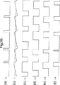
The jitter reduction operation of this circuit will be described with reference to FIGS. 2 (a) to 2 (d). With jitter, one pulse is time t j A train M of five pulses from the input monostable circuit, misplaced by only one, is shown in FIG. The corresponding integrator output N is shown in FIG. 2 (b) together with the comparator output O (FIG. 2 (c)) and the output P from the output monostable circuit 5 (FIG. 2 (d)).
The
[0022]
If the DC component is correctly removed, the operation of the circuit is as follows. As can be seen from FIG. 2A to FIG. 2D, the time for the comparator 4 to switch to the positive slope of the integrator waveform N is the time jitter t of the center pulse of the waveform M. j Is not affected at all. The fact that the pulse positive edge of the waveform O is independent of the time jitter means that the output waveform from the monostable circuit P has no jitter. The circuit actually eliminated the time jitter and phase noise of the input waveform and provided a jitter free waveform with the same average frequency as the input.
[0023]
A phase noise reduction or
[0024]
In this circuit, the
[0025]
This frequency doubler operates if both the “mark” and “space” periods of the input waveform are longer than the timing period of the short pulse monostable circuit.
[0026]
The
[0027]
[0028]
FIG. 4 (a) illustrates an advantageous design of the short pulse monostable circuit used in circuit 33. Referring to this figure, the
[0029]
FIG. 4 (b) illustrates an advantageous design for the two short pulse
[0030]
Depending on the mode of use, adding a load resistor inside and / or between the NAND gates of FIGS. 4 (a) and 4 (b) allows the pulse length to be sufficient for use as a fixed pulse length monostable circuit. Can be made constant.
[0031]
FIG. 5 illustrates a clock recovery circuit having functions common to the
[0032]
This circuit has as its input an electrical signal waveform or pulse train with a pronounced periodicity, but the individual rising and falling edges are not precise time intervals, i.e. affected by phase noise and are individually The wave or pulse or set of waves or pulses may be completely missing.
[0033]
An input pulse train or waveform S ″ with missing pulses and time jitter is first supplied to a short pulse
[0034]
The
[0035]
Accordingly, the
[0036]
In this way, the output pulse train is reconstructed with each reinsertion pulse delayed with respect to the timing of the missing pulse. This circuit can insert a long train of pulses if several input pulses are missing. The waveforms that occur when this occurs are illustrated in FIGS. 6 (a) to 6 (d).
[0037]
Finally, an optional
[0038]
If a long sequence of input pulses is missing, the circuit continues to operate at the original input frequency for a time that does not exceed the time constant of the DC rejection circuit. This time is significantly increased by the optional circuit configuration also shown in FIG.
[0039]
This optional circuit configuration includes a
[0040]
The frequency drift of the inserted pulse is a specific frequency F p There are situations where it is desirable to have an
[0041]
The circuit block indicated by 68 constitutes a missing pulse insertion circuit, which may be used as a subsystem in other circuits.
[0042]
An alternative
[0043]
As can be seen,
[0044]
Further examination shows that the voltage of the
[0045]
In addition, if the voltage at
[0046]
The circuit is precisely phase-locked to a selected multiple of the input frequency and remains phase-locked to this multiple even if the input frequency changes over a substantial range. In this way, the clock recovery circuit operates as a general purpose frequency multiplier. In this case, a second anti-jitter circuit may be used to equalize the pulse interval and eliminate phase timing jumps that occur for pulses reinserted between actual input clock pulses.
[0047]
Finally, in the case of multiple periodicities, the circuit may be arranged to lock on to selected spectral components of the input signal corresponding to a particular periodicity. This is accomplished by preconditioning the circuit with a desired periodic pulse train or by presetting the voltage across the
[0048]
According to another aspect of the present invention, the noise reduction circuit is effective in removing spurious added pulses, ie pulses added to pulses of the nominal input frequency f, from the input pulse train. As before, the noise reduction circuit includes a jitter prevention circuit that may reduce or eliminate time jitter in the pulse train. A noise reduction circuit according to this aspect of the invention will now be described by way of example with respect to FIGS.
[0049]
FIG. 8 illustrates a
[0050]
Input pulse train or waveform S * Is affected by time jitter and includes spurious additional pulses.
[0051]
Input pulse train or waveform S * Is first taken into the AND
[0052]
Pulse train B * The period T in which the AND
[0053]
[0054]
FIG. 9 illustrates an
[0055]
However, in this circuit, the output of the
[0056]
The
[0057]
FIGS. 10 (a) to 10 (d) show waveforms seen at various points in
[0058]
FIG. 11 shows an anti-jitter and spurious
[0059]
FIG. 13 shows a
[0060]
[0061]
In the case of
[0062]
FIG. 15 shows a
[0063]
[0064]
In another embodiment, two pulse deletion circuits of the type described are used. One acts on the input waveform and the other acts on the polarity reversal of the input waveform. The output pulse train from the pulse deletion circuit is supplied to different divide-by-2 circuits, and their outputs are combined by an OR gate to form one common output. Also, the output pulse train from the pulse deletion circuit may be supplied to set and reset the input of the flip-flop circuit, and the output of the flip-flop circuit may form one common output.
[0065]
[0066]
For all circuits described herein, modifications will be apparent to those skilled in the art of electronic circuitry, but this is not a significant change from the present invention. For example, a set of logic gates may be replaced by an alternative set having the same mathematical function (Boolean logic function) as the present invention.
[0067]
[0068]
In applications involving a clock signal, there is a need to provide a single clock signal having an adjustable phase and / or mark-to-space ratio for the input pulse train, even though it has a constant nominal frequency. In another application, it is necessary to provide two or more clock signals having the same nominal frequency but having different phases and / or mark-to-space ratios with respect to each other and / or the input pulse train. Another aspect of the present invention provides a noise reduction circuit for use in applications such as multi-phase, multi-output clock distribution circuits.
[0069]
FIG. 16 illustrates a phase noise reduction circuit that generates a single clock signal. This circuit uses a double comparator set / reset latch output.
[0070]
FIGS. 17 (a) to 17 (e) illustrate voltage waveforms observed at various points in the circuit of FIG.
[0071]
Referring to FIG. 16, the pulse train S 1 Is the input to
[0072]
[0073]
In order to speed up the response of the circuit to changes in input frequency, a speed-up circuit as described with respect to FIGS. 1 and 3 may be used. It comprises two series back-to-back Zener diodes connected from the output of the
[0074]
Input pulse train S 1 And the phase relationship between the output pulse train O and the voltage V applied to the
[0075]
The described circuit arrangement has the advantage that jitter is reduced at both the rising and falling edges. This has the advantage that it can handle input pulse trains over a wider input frequency range without the need for an input frequency doubler and an output divide-by-2 circuit. This has the additional advantage that the interval between the trigger times of the comparators increases as the frequency decreases because the amplitude of the sawtooth waveform output by the
[0076]
FIG. 18 shows an anti-jitter circuit that can generate a multi-phase output, eg, a multi-phase clock signal.
[0077]
Another way to achieve similar length clock pulses in a multi-phase clock generator based on an anti-jitter circuit with a narrow range of input frequencies is shown in FIG.
[0078]
The anti-jitter circuit described in accordance with this aspect of the invention is a T.I. V. Suitable for multi-phase output circuit configuration of the kind described in Rama Murthy's paper "Continuous Phase Shifter for Square Waves", Electronics, mid-April 1979,
[0079]
Another aspect of the present invention relates to a low noise fractional rate multiplier circuit, and more particularly, but not exclusively, to a low noise fractional rate multiplier circuit useful in a fractional N phase locked loop synthesizer.
[0080]
In electronics, it is often necessary to generate a new periodic electrical signal source with a frequency that is a multiple or fraction of a fixed reference periodic signal source. The new signal has jitter. That is, the signal edge changes with respect to the signal edge of an accurate periodic signal having the same frequency. It is an object of this aspect of the invention to reduce this jitter. In the following description, phase noise is referred to as jitter. Since phase noise is proportional to jitter, one reduction is equivalent to the other.
[0081]
In the following examples, the anti-jitter circuit (AJC) used is of the type described in WO 97/30516, such as the circuit described with respect to FIGS. 1 to 3 of the accompanying drawings.
[0082]
Instead of using one AJC, it is alternatively possible to use a series of two or more AJCs interconnected so that the output of one AJC becomes the output of another AJC. The jitter reduction made by the first AJC is increased by the next AJC, and so on. For example, if one AJC has a jitter reduction of 20 dB, ideally a cascade of two such AJC circuits will have a jitter reduction of 40 dB, and ideally a cascade of three AJCs will have a jitter of 60 dB. Has a reduction. In practice, since this process is limited by the noise performance of the AJC component, jitter reduction is significantly reduced for each circuit greater than two. Therefore, there is little value in using more than three AJC circuits in cascade.
[0083]
In relatively simple applications, a fast reference source is used as the source from which the desired low frequency is obtained.
[0084]
The simplest way to use AJC in frequency synthesis is to add 1 to a module-N divider applied to high frequency sources. The module N divider reduces the jitter with respect to the period of the output waveform exactly by the division ratio N (modulus of division N). However, residual jitter can be further reduced by using AJC. If AJC is obtained at a sufficiently high operating frequency, AJC is directly applied to high frequency (HF) standards. Otherwise, AJC is the initial divider stage N i Applied after AJC and further N after AJC o Divided by N, where N i ・ N o = N.
[0085]
AJC circuits have a greater impact than when used directly with certain rate multiplier circuits. The function of the fractional rate multiplier circuit is to output A pulses for every B input pulses when A changes from 1 to 1000, for example, and B is constant at 1000. That is, the input frequency is multiplied by A / B. Several designs of fractional rate multipliers are possible, but they depend on the amount of inherent jitter that the output has.
[0086]
A particularly convenient form of rate multiplier is that of a type (Sequential Addition Rate Multiplier or SARM) that sequentially adds a constant number of phase increments to the accumulator and provides an output each time the accumulator overflows. is there. This has the advantage of operating by skipping pulses in the input pulse train so that the maximum output jitter is less than one full period of the output waveform. Since this type of waveform is correctly de-jittered by AJC, SARM is easily enhanced by the addition of AJC. (Note that a direct digital frequency synthesizer (DDS) with 1-bit output is equivalent to SARM). FIG. 25 shows how one AJC circuit or even better two AJC circuits in series can reduce spurious 500 kHz components in a 10 MHz signal.
[0087]
Simple rate multipliers such as BCD rate multiplier HEF4527 (see "HE4000B Logic Device Family CMOS Handbook", Philips Semiconductor PO Box 218, 5600 MD Eindhoven) have high inherent output jitter with multiplication by 7/10. Have For example, HEF 4527 provides 4 pulses per unit interval, then a gap of missing pulses, then 3 pulses per unit interval, then a gap of double missing pulses, ie maximum output jitter that exceeds an entire output period. . These waveforms (and similar waveforms from cascaded HEF4527 circuits) are too jittery and cannot be successfully defeated by direct AJC. Instead, there must be a divider after the fractional rate multiplier before AJC is applied. For a typical BCD multiplier, the required divider can have any integer division ratio greater than or equal to two. If the divide-by-2 output frequency is unacceptable, the output can be doubled using a range of known multiplier circuits, such as a double harmonic multiplier.
[0088]
In order to efficiently provide a large number of possible divide ratios, more sophisticated methods using dividers and AJC, such as those involving pulse subtraction, are beneficial.
[0089]
Referring to FIG. 21, the
[0090]
22 (a) to 22 (e) show typical waveforms observed at various points in the circuit of FIG. 21 where AJC is used to suppress jitter in the output of the rate multiplier. The box in FIG. 22 indicates that the rate multiplier has an input pulse S. 2 Waveform S with jitter by subtracting 1 for every 5 2 One complete cycle of generating '. The waveform of the integrator inside the
[0091]
One example is considered to illustrate the operation of the circuit. Input pulse train S 2 Has an input frequency of 100 MHz and N a Is set to 100 and A a Is set to 100 and N a 'Is set to 1 (equivalent to omitting the
F o = F i / (N a + A a )
Where F i And F o Are the input and output frequencies, respectively. This gives a divided output frequency of 995.025 kHz for the example cited above.
[0092]
Obviously, in this example, N a And A a With this setting, 10,000 individual frequencies can be selected. These are the possibilities using the circuit according to FIG. 21 with an input frequency of 100 MHz. A a Is variable from 0.01 to 0.01 0.99, N a Is variable from 201 to 1. The selectable frequencies are spread evenly throughout the spectrum and the spacing is a percentage of the output frequency, increasing from 0.005% at 500 kHz output to 1% in the worst case (near 100 MHz).
[0093]
Such a setting is tied to setting the
[0094]
An alternative embodiment of the present invention shown in FIG. 23 uses a
[0095]
If an output frequency is needed, which probably exceeds the available reference frequency, for example, “Radio Receiver” W Gosling (eds.), Peter Peregrinus Ltd, 1996, Chapter 4 “Frequency Synthesizers and Standards” M Underhill, ISBN A phase locked loop (PLL) concept is used as described in -0-86341056. Using this concept, the voltage controlled oscillator that provides the output is phase locked to an exact multiple (possibly a fractional multiple) of the reference frequency. By using the AJC circuit in the PLL circuit, the fractional N synthesis can be performed without deterioration of normal jitter performance.
[0096]
Referring to FIG. 24, a fractional N frequency synthesizer incorporating a low noise
[0097]
The selection of N, N ′ and N ″ is determined as follows.
[0098]
N ″ is ideally 1 (ie, no prescaler), but for very high frequency VCOs, the programmable divider may not be able to operate at the maximum VCO frequency (programmable). Many of the dividers operate more than 3 times slower than a simple prescaler flip-flop circuit. In this case, it is usually sufficient to use a small factor N ″, possibly 2 or 4 or 8. This approach is also used to minimize the overall power consumption of the synthesizer system because of the high power consumption of the high speed logic elements used for the prescaler. N ′ is also ideally 1 (ie, no divider before AJD 435). However,
[0099]
The programmable divider is advantageously of the multiple feedback type exemplified by the Philips HEF4751 and SAA1057 frequency synthesizer integrated circuits.
[0100]
The coefficient A of the fractional rate multiplier is selected to subtract the pulse at a frequency that can be phase synchronized after tuning the VCO to the required output frequency (lowering the comparison frequency applied to the phase comparator).
[0101]
For example, for a 100 kHz reference oscillator and a VCO capable of generating 100 MHz to 1 GHz, the dividers N, N ′ and N ″ need to be set to achieve a division ratio of 1000 to 10,000. N ″ is 1. And N ′ = 10 and N = 500. In this way, the circuit phase comparator transfers the voltage to the VCO, which rises to 500 MHz. Suppose the fractional rate multiplier is set to subtract every 1000th pulse (rate multiplication A of 0.999). In this manner, every 1000 pulses, ie every 10 milliseconds, pulses are removed from the oscillator output. This reduces the frequency of the input to the divider from one pulse every 10 milliseconds, ie from 500.000000 MHz to 499.999900 MHz. This lower frequency input is seen at the phase comparator, from which the increased voltage is transferred to the VCO, where the frequency rises from 500.000000 MHz to 500.000010 MHz after a small system time constant. It is easy to show that by proper selection of N (and N ′, N ″) and A, the VCO can be phase synchronized to any one of 9 million frequencies from 100 MHz to 1 GHz.
[0102]
A fractional N synthesizer with AJC constructed in accordance with this aspect of the invention has shown that improved performance can be achieved. In this example, a Motorola integrated
FIG. 26 shows the jitter suppression effect by AJC of (a) 6.991 kHz and (b) 139.82 Hz components in the output of the fractional N frequency synthesizer according to the present invention. The reference and its harmonic spurious signals are greatly suppressed by the AJC of the divider chain. The reduction of 19 dB in the components at the 6991 kHz interval was unexpectedly large. The 10 dB reduction in components at 139.82 Hz spacing would be improved by the use of a sample / hold or high gain phase comparator rather than the type of pulse width actually utilized in this demonstration (the phase comparator's Performance degradation hides the jitter improvement achieved by AJC).
[0103]
In general, the pulse subtractor and pulse inserter used in the circuits of FIGS. 21, 23 and 24 increase the inherent jitter of the input pulse train. Similarly, the fractional rate multiplier effectively deletes the pulses input thereto, but this also generates jitter. However, the AJC circuits used in these circuits can reduce this additional source of jitter (similar to intrinsic jitter) by 20 dB or more. Jitter is further reduced in this system by a factor of N, ie the ratio of the programmable divider.
[0104]
The described pulse subtractor is replaced by a circuit comprising a variable modulus divider and a counter. As an example, a divider with a nominal divider ratio of 10 can be switched to divide by a factor of 11 for a given set of 110 consecutive input pulses in response to a control signal. That is, 10 pulses are output instead of 11 for 110 pulses. Even a simple circuit can be switched to divide by either 1 or 2. Each time the circuit is commanded to divide by 2, it effectively removes one of the input pulses.
[0105]
Similarly, the described pulse inserter is replaced by a circuit including a variable divider ratio divider and a counter. For example, a divider having a nominal division ratio of 10 can be switched to divide by 9 for a given set of 90 consecutive input pulses. That is, 10 pulses are output instead of 9 for 90 pulses.
[0106]
For all circuits described herein, modifications will be apparent to those skilled in the art of electronic circuitry, but this is not a significant departure from the present invention. For example, a set of logic gates may be replaced by an alternative set having the same mathematical function (Boolean logic function).
[0107]
As already explained, the circuit according to the invention is applied in particular to the restoration of clock signals and other regular pulse trains of communication circuits that are affected by other problems that cause noise, interference, crosstalk or jitter. .
[Brief description of the drawings]
FIG. 1 is a diagram illustrating a known phase noise reduction circuit.
2 (a) to 2 (d) are diagrams showing various waveforms that are useful in understanding the operation of the phase noise reduction circuit of FIG.
FIG. 3 is a diagram showing a phase noise reduction circuit according to the present invention.
4 (a) and 4 (b) are diagrams showing a short pulse monostable circuit used in the phase noise reduction circuit of FIG.
FIG. 5 is a diagram illustrating a clock recovery circuit according to the present invention.
6 (a) to 6 (d) are diagrams showing various waveforms useful in understanding the operation of the clock recovery circuit of FIG.
FIG. 7 is a diagram illustrating another clock recovery circuit according to the present invention.
FIG. 8 is a diagram illustrating a clock recovery circuit according to the present invention.
FIG. 9 is a diagram illustrating an alternative clock recovery circuit according to the present invention.
10 (a) to 10 (d) are diagrams showing voltage waveforms observed at various points in the circuit of FIG.
FIG. 11 is a diagram illustrating a jitter prevention and spurious pulse deletion circuit having a frequency doubled input.
12 (a) to 12 (d) are diagrams showing voltage waveforms observed at various points in the circuit of FIG.
FIG. 13 is a diagram illustrating a latch circuit.
FIG. 14 is a diagram illustrating a clock recovery circuit incorporating the latch circuit of FIG. 13;
FIG. 15 is a diagram illustrating another clock recovery circuit;
FIG. 16 is a diagram showing a phase noise reduction circuit according to the present invention.
17 (a) to 17 (e) are diagrams showing voltage waveforms observed at various points in the circuit of FIG.
FIG. 18 is a diagram illustrating an alternative phase noise reduction circuit.
FIG. 19 is a diagram illustrating an alternative phase noise reduction circuit.
20 (a) to 20 (f) are diagrams showing voltage waveforms observed at various points in the circuit of FIG.
FIG. 21 is a diagram showing a fractional rate multiplier circuit according to the present invention.
22 (a) and 22 (b) are diagrams showing voltage waveforms observed at various points in the circuit of FIG.
FIG. 23 is a diagram illustrating an alternative fractional rate multiplier circuit in accordance with the present invention.
FIG. 24 is a diagram showing a fractional N frequency synthesizer including the fractional rate multiplication circuit of FIG. 21 or FIG.
FIGS. 25 (a), 25 (b), and 25 (c) operate at 10.1 MHz, which occurs in the case of no AJC, one AJC, and two cascaded AJCs, respectively. It is a figure which shows the frequency spectrum of the output of 1 bit DDS.
FIGS. 26 (a) and 26 (b) are diagrams showing the effect of suppression by AJC of the 69991 kHz component and the 139.82 Hz component of the output of the fractional N frequency synthesizer according to the present invention, respectively.
Claims (39)
前記入力パルス列から直流レベルを除去する直流除去手段と、
前記直流除去手段によって直流レベルが除去された後前記入力パルス列を積分する積分手段と、
前記積分手段からの出力を受信し、該出力から前記入力パルス列の欠落パルスを検出する検出手段と、
前記検出手段に応答して、前記検出手段によって検出された前記欠落パルスに関して遅延された付加パルスを前記入力パルス列に挿入するパルス生成手段と、
前記積分手段からの前記出力から出力パルス列を生成する出力手段とを備えるクロック復元回路。A clock recovery circuit for reducing noise in an input pulse train comprising a plurality of pulses having a nominal periodicity , from which one or more pulses are missing ,
A DC removal means for removing a DC level from the entering force pulse train,
An integrating means for integrating the input pulse train after a DC level has been removed by the previous SL DC removal means,
Receives the output from the previous SL integrating means, a detecting means for detecting a missing pulse in the input pulse train from the output,
In response before Symbol detection means, pulse generating means for inserting delayed additional pulse with respect to the missing pulses detected by said detecting means to said input pulse train,
The clock recovery circuit and an output means for generating an output pulse train from the output from the previous SL integrating means.
前記入力パルス列から第1パルス列を得る手段であって、前記第1パルス列が前記入力パルス列を形成するパルスの正方向変換点によってトリガされるパルスからなる手段と、
前記入力パルス列から第2パルス列を得る手段であって、前記第2パルス列が前記入力パルス列を形成するパルスの負方向変換点によってトリガされるパルスからなる手段と、
結合パルス列を形成するために前記第1及び第2パルス列を結合する結合手段と、
前記結合パルス列から直流レベルを除去する直流除去手段と、
積分出力を生成するために前記直流除去手段によって前記直流レベルが除去された後前記結合パルス列を積分する積分手段と、
前記公称周波数fの出力パルス列を前記積分出力から得る処理手段とを備える回路。A phase noise reduction circuit for reducing phase noise of the input pulse train consisting of pulses having a nominal frequency f,
A means for obtaining a first pulse train from the entering force pulse train, and means including a pulse by the first pulse train is triggered by the positive direction conversion point of the pulses forming the input pulse train,
And means for obtaining a second pulse train from the entering force pulse train, and means comprising a pulse the second pulse train is triggered by the negative direction change points of the pulses forming the input pulse train,
And coupling means for coupling said first and second pulse trains to form a binding pulse train,
A DC removal means for removing a DC level from the pre-Symbol coupling pulse train,
An integrating means for integrating the combined pulse train after the DC level has been removed by the DC removal means to produce a product fraction output,
Circuit and a processing means for obtaining an output pulse train of the previous SL nominal frequency f from the integrator output.
前記入力パルス列から直流レベルを除去する直流レベル除去手段と、
前記直流除去手段によって前記入力パルス列から前記直流レベルが除去された後、該入力パルス列を積分する積分手段と、
前記入力パルス列から前記スプリアス付加パルスを削除するパルス削除手段であって、前記積分手段からの出力を受信し且つ該出力に応答してブランキング・パルスを生成するパルス生成手段と、前記1つかそれ以上のスプリアス付加パルスを削除するために前記ブランキング・パルスを前記入力パルス列の前記複数のパルスに結合する手段と、を備えるパルス削除手段と、
前記積分手段の出力から出力パルス列を得る出力手段とを備えるクロック復元回路。A clock recovery circuit for reducing noise in an input pulse train comprising a plurality of pulses having a nominal periodicity in which one or more spurious additional pulses are present ,
A DC level removal means for removing a DC level from the entering force pulse train,
After the DC level from the input pulse train is removed by the pre-Symbol DC removal means, an integrating means for integrating the input pulse train,
A pulse deletion means for deleting the spurious additional pulses from the entering force pulse train, pulse generating means for generating a blanking pulse in response to the received and output the output from said integrating means, said one or Means for coupling the blanking pulse to the plurality of pulses of the input pulse train to remove further spurious additive pulses ; and
The clock recovery circuit and an output means for the output of the previous SL integrating means obtaining an output pulse train.
前記入力パルス列から直流レベルを除去する直流除去手段と、
前記直流除去手段によって前記入力パルス列から直流レベルを除去した後前記入力パルス列を積分する積分手段と、
前記積分手段からの出力及びそれぞれ異なった基準信号に応答して異なった出力パルス列を発生し、それによって前記出力パルス列の各々が対応する前記基準信号に応じて前記入力パルス列の変換点に対するそれぞれの位相関係を有する周期的変換点を含む少なくとも2つの検出手段とを含む回路。A circuit for reducing phase noise of an input pulse train composed of a plurality of pulses having nominal periodicity ,
A DC removal means for removing a DC level from the entering force pulse train,
An integrating means for integrating the input pulse train after removing the DC level from the input pulse train by a pre-Symbol DC removal means,
Generates an output pulse train differently in response to the output and each different reference signals from before Symbol integrating means, whereby each for converting points of the input pulse train in response to the reference signal, each of said output pulse train corresponding A circuit including at least two detection means including a periodic conversion point having a phase relationship.
Applications Claiming Priority (9)
| Application Number | Priority Date | Filing Date | Title |
|---|---|---|---|
| GBGB9714309.3A GB9714309D0 (en) | 1997-07-07 | 1997-07-07 | Noise reduction circuits |
| GB9714309.3 | 1997-07-07 | ||
| GB9716041.0 | 1997-07-30 | ||
| GBGB9716041.0A GB9716041D0 (en) | 1997-07-30 | 1997-07-30 | Jitter reduction and spurious pulse deletion circuit for noise reduction |
| GBGB9719291.8A GB9719291D0 (en) | 1997-09-10 | 1997-09-10 | Jitter reduction circuit with application to multiphase output clock distribut on |
| GB9719291.8 | 1997-09-10 | ||
| GB9805017.2 | 1998-03-11 | ||
| GBGB9805017.2A GB9805017D0 (en) | 1998-03-11 | 1998-03-11 | Fractional-n frequency synthesiser with jitter suppression |
| PCT/GB1998/002001 WO1999003201A2 (en) | 1997-07-07 | 1998-07-06 | Missing pulse detector |
Publications (3)
| Publication Number | Publication Date |
|---|---|
| JP2001510291A JP2001510291A (en) | 2001-07-31 |
| JP2001510291A5 JP2001510291A5 (en) | 2006-01-05 |
| JP4065365B2 true JP4065365B2 (en) | 2008-03-26 |
Family
ID=27451675
Family Applications (1)
| Application Number | Title | Priority Date | Filing Date |
|---|---|---|---|
| JP2000502578A Expired - Fee Related JP4065365B2 (en) | 1997-07-07 | 1998-07-06 | Noise reduction circuit |
Country Status (7)
| Country | Link |
|---|---|
| US (1) | US6417707B1 (en) |
| EP (1) | EP1040577B1 (en) |
| JP (1) | JP4065365B2 (en) |
| KR (1) | KR100514549B1 (en) |
| AU (1) | AU8232898A (en) |
| DE (1) | DE69840525D1 (en) |
| WO (1) | WO1999003201A2 (en) |
Families Citing this family (17)
| Publication number | Priority date | Publication date | Assignee | Title |
|---|---|---|---|---|
| US6434707B1 (en) | 1999-06-07 | 2002-08-13 | Motorola, Inc. | Low phase jitter clock signal generation circuit |
| US6981166B2 (en) * | 2002-01-07 | 2005-12-27 | International Business Machines Corporation | Method, apparatus, and computer program product for pacing clocked operations |
| DE602004025907D1 (en) * | 2004-06-04 | 2010-04-22 | Infineon Technologies Ag | Device for DC compensation in a demodulator |
| GB0416627D0 (en) * | 2004-07-26 | 2004-08-25 | Toric Ltd | Anti-jitter circuits |
| CN101065900A (en) * | 2004-11-26 | 2007-10-31 | 皇家飞利浦电子股份有限公司 | Jitter reduction circuit and frequency synthesizer |
| JP4748356B2 (en) * | 2005-10-13 | 2011-08-17 | サンケン電気株式会社 | Induction heating device |
| US7961086B2 (en) * | 2006-04-17 | 2011-06-14 | James Roy Bradley | System and method for vehicular communications |
| US20080122606A1 (en) * | 2006-04-17 | 2008-05-29 | James Roy Bradley | System and Method for Vehicular Communications |
| DE102007002112B4 (en) * | 2007-01-15 | 2008-12-18 | Infineon Technologies Ag | Apparatus and method for regenerating a clock signal, apparatus and method for converting a clock signal into a mean-free signal |
| US20080253491A1 (en) * | 2007-04-13 | 2008-10-16 | Georgia Tech Research Corporation | Method and Apparatus for Reducing Jitter in Multi-Gigahertz Systems |
| GB0807152D0 (en) * | 2008-04-18 | 2008-05-21 | Toric Ltd | Clock generator circuits |
| US8924765B2 (en) * | 2011-07-03 | 2014-12-30 | Ambiq Micro, Inc. | Method and apparatus for low jitter distributed clock calibration |
| JP5657596B2 (en) * | 2012-03-26 | 2015-01-21 | 株式会社東芝 | Proximity interference removal filter device, wireless communication device, and keyless entry device |
| TWM445301U (en) * | 2012-09-06 | 2013-01-11 | Excelliance Mos Corp | Voltage converting apparatus and sub-harmonic detector thereof |
| CN105242678B (en) * | 2015-09-11 | 2017-10-31 | 湖北三江航天红峰控制有限公司 | A kind of steering gear swaying suppression circuit and steering gear system |
| CN109302177A (en) * | 2018-11-27 | 2019-02-01 | 国网上海市电力公司 | A kind of digital feedback precision square wave phase shifter based on two frequency multiplication two divided-frequencies |
| RU2719556C1 (en) * | 2019-07-30 | 2020-04-21 | федеральное государственное бюджетное образовательное учреждение высшего образования "Белгородский государственный технологический университет им. В.Г. Шухова" | Periodic pulse train shaper |
Family Cites Families (8)
| Publication number | Priority date | Publication date | Assignee | Title |
|---|---|---|---|---|
| GB1462408A (en) | 1974-07-26 | 1977-01-26 | Mullard Ltd | Circuit for comparing two electrical waveforms |
| US4230958A (en) * | 1978-08-09 | 1980-10-28 | Bell Telephone Laboratories, Incorporated | Loss of clock detector circuit |
| GB2064273B (en) | 1979-11-23 | 1983-10-19 | Marconi Co Ltd | Data transmission clock pulse recovery |
| JPH0453366A (en) | 1990-06-21 | 1992-02-20 | Matsushita Electric Ind Co Ltd | Horizontal synchronizing signal separator |
| GB2274032A (en) | 1993-01-05 | 1994-07-06 | Mitel Corp | Clock-sensitive processor reset circuit |
| JPH08163181A (en) * | 1994-11-30 | 1996-06-21 | Sharp Corp | Information reproduction circuit |
| GB2310331B (en) | 1996-02-15 | 2000-06-28 | Surrey University Of | Phase noise reduction circuits |
| US5742200A (en) * | 1996-05-14 | 1998-04-21 | Alliedsignal Inc. | Environmentally rugged optical sensor with improved noise cancellation |
-
1998
- 1998-07-06 DE DE69840525T patent/DE69840525D1/en not_active Expired - Fee Related
- 1998-07-06 JP JP2000502578A patent/JP4065365B2/en not_active Expired - Fee Related
- 1998-07-06 EP EP98932394A patent/EP1040577B1/en not_active Expired - Lifetime
- 1998-07-06 AU AU82328/98A patent/AU8232898A/en not_active Abandoned
- 1998-07-06 US US09/446,648 patent/US6417707B1/en not_active Expired - Fee Related
- 1998-07-06 KR KR10-2000-7000164A patent/KR100514549B1/en not_active IP Right Cessation
- 1998-07-06 WO PCT/GB1998/002001 patent/WO1999003201A2/en active IP Right Grant
Also Published As
| Publication number | Publication date |
|---|---|
| AU8232898A (en) | 1999-02-08 |
| KR20010021606A (en) | 2001-03-15 |
| EP1040577B1 (en) | 2009-01-28 |
| WO1999003201A2 (en) | 1999-01-21 |
| JP2001510291A (en) | 2001-07-31 |
| KR100514549B1 (en) | 2005-09-14 |
| DE69840525D1 (en) | 2009-03-19 |
| US6417707B1 (en) | 2002-07-09 |
| EP1040577A2 (en) | 2000-10-04 |
| WO1999003201A3 (en) | 1999-03-25 |
Similar Documents
| Publication | Publication Date | Title |
|---|---|---|
| JP4065365B2 (en) | Noise reduction circuit | |
| US6714056B2 (en) | Frequency division/multiplication with jitter minimization | |
| EP0526227A2 (en) | Phase-locked loop | |
| EP2434647A2 (en) | Injection-locked oscillator | |
| US6642800B2 (en) | Spurious-free fractional-N frequency synthesizer with multi-phase network circuit | |
| US8269536B2 (en) | Onion waveform generator and spread spectrum clock generator using the same | |
| US10784844B2 (en) | Fractional frequency divider and frequency synthesizer | |
| JP3611589B2 (en) | Fractional N divider | |
| US6538516B2 (en) | System and method for synchronizing multiple phase-lock loops or other synchronizable oscillators without using a master clock signal | |
| US7606343B2 (en) | Phase-locked-loop with reduced clock jitter | |
| US6275101B1 (en) | Phase noise reduction circuits | |
| US7023945B2 (en) | Method and apparatus for jitter reduction in phase locked loops | |
| US11784651B2 (en) | Circuitry and methods for fractional division of high-frequency clock signals | |
| EP2629424A1 (en) | Frequency synthesizer | |
| EP0966103B1 (en) | Frequency synthesiser | |
| KR19980033965A (en) | Clock and Data Recovery Circuit for Optical Communication Receiver | |
| KR100247006B1 (en) | Dpll building zero phase error | |
| RU1774497C (en) | Automatic phase locking unit | |
| JP2019009584A (en) | PLL circuit | |
| JPS5964928A (en) | Oscillating device | |
| JPS6058621B2 (en) | Continuous clock generation method | |
| JPH03250814A (en) | Frequency synthesizer | |
| KR20010038586A (en) | Apparatus for digital timing recovery | |
| JPH11284507A (en) | Semiconductor integrated circuit device | |
| JP2003168974A (en) | Synchronization method and synchronization circuit |
Legal Events
| Date | Code | Title | Description |
|---|---|---|---|
| A521 | Written amendment |
Free format text: JAPANESE INTERMEDIATE CODE: A523 Effective date: 20050706 |
|
| A621 | Written request for application examination |
Free format text: JAPANESE INTERMEDIATE CODE: A621 Effective date: 20050706 |
|
| A711 | Notification of change in applicant |
Free format text: JAPANESE INTERMEDIATE CODE: A711 Effective date: 20060117 |
|
| A521 | Written amendment |
Free format text: JAPANESE INTERMEDIATE CODE: A821 Effective date: 20060117 |
|
| A131 | Notification of reasons for refusal |
Free format text: JAPANESE INTERMEDIATE CODE: A131 Effective date: 20070410 |
|
| A601 | Written request for extension of time |
Free format text: JAPANESE INTERMEDIATE CODE: A601 Effective date: 20070709 |
|
| A602 | Written permission of extension of time |
Free format text: JAPANESE INTERMEDIATE CODE: A602 Effective date: 20070717 |
|
| A521 | Written amendment |
Free format text: JAPANESE INTERMEDIATE CODE: A523 Effective date: 20071010 |
|
| TRDD | Decision of grant or rejection written | ||
| A01 | Written decision to grant a patent or to grant a registration (utility model) |
Free format text: JAPANESE INTERMEDIATE CODE: A01 Effective date: 20071204 |
|
| A61 | First payment of annual fees (during grant procedure) |
Free format text: JAPANESE INTERMEDIATE CODE: A61 Effective date: 20080104 |
|
| R150 | Certificate of patent or registration of utility model |
Free format text: JAPANESE INTERMEDIATE CODE: R150 |
|
| FPAY | Renewal fee payment (event date is renewal date of database) |
Free format text: PAYMENT UNTIL: 20110111 Year of fee payment: 3 |
|
| LAPS | Cancellation because of no payment of annual fees |