JP4060185B2 - Wafer handling system with reduced edge contact, modification method and use thereof - Google Patents
Wafer handling system with reduced edge contact, modification method and use thereof Download PDFInfo
- Publication number
- JP4060185B2 JP4060185B2 JP2002547208A JP2002547208A JP4060185B2 JP 4060185 B2 JP4060185 B2 JP 4060185B2 JP 2002547208 A JP2002547208 A JP 2002547208A JP 2002547208 A JP2002547208 A JP 2002547208A JP 4060185 B2 JP4060185 B2 JP 4060185B2
- Authority
- JP
- Japan
- Prior art keywords
- wafer
- chuck
- support surface
- arm
- transfer
- Prior art date
- Legal status (The legal status is an assumption and is not a legal conclusion. Google has not performed a legal analysis and makes no representation as to the accuracy of the status listed.)
- Expired - Lifetime
Links
Images


Classifications
-
- H—ELECTRICITY
- H01—ELECTRIC ELEMENTS
- H01L—SEMICONDUCTOR DEVICES NOT COVERED BY CLASS H10
- H01L21/00—Processes or apparatus adapted for the manufacture or treatment of semiconductor or solid state devices or of parts thereof
- H01L21/67—Apparatus specially adapted for handling semiconductor or electric solid state devices during manufacture or treatment thereof; Apparatus specially adapted for handling wafers during manufacture or treatment of semiconductor or electric solid state devices or components ; Apparatus not specifically provided for elsewhere
- H01L21/683—Apparatus specially adapted for handling semiconductor or electric solid state devices during manufacture or treatment thereof; Apparatus specially adapted for handling wafers during manufacture or treatment of semiconductor or electric solid state devices or components ; Apparatus not specifically provided for elsewhere for supporting or gripping
- H01L21/687—Apparatus specially adapted for handling semiconductor or electric solid state devices during manufacture or treatment thereof; Apparatus specially adapted for handling wafers during manufacture or treatment of semiconductor or electric solid state devices or components ; Apparatus not specifically provided for elsewhere for supporting or gripping using mechanical means, e.g. chucks, clamps or pinches
- H01L21/68714—Apparatus specially adapted for handling semiconductor or electric solid state devices during manufacture or treatment thereof; Apparatus specially adapted for handling wafers during manufacture or treatment of semiconductor or electric solid state devices or components ; Apparatus not specifically provided for elsewhere for supporting or gripping using mechanical means, e.g. chucks, clamps or pinches the wafers being placed on a susceptor, stage or support
- H01L21/68728—Apparatus specially adapted for handling semiconductor or electric solid state devices during manufacture or treatment thereof; Apparatus specially adapted for handling wafers during manufacture or treatment of semiconductor or electric solid state devices or components ; Apparatus not specifically provided for elsewhere for supporting or gripping using mechanical means, e.g. chucks, clamps or pinches the wafers being placed on a susceptor, stage or support characterised by a plurality of separate clamping members, e.g. clamping fingers
-
- H—ELECTRICITY
- H01—ELECTRIC ELEMENTS
- H01L—SEMICONDUCTOR DEVICES NOT COVERED BY CLASS H10
- H01L21/00—Processes or apparatus adapted for the manufacture or treatment of semiconductor or solid state devices or of parts thereof
- H01L21/67—Apparatus specially adapted for handling semiconductor or electric solid state devices during manufacture or treatment thereof; Apparatus specially adapted for handling wafers during manufacture or treatment of semiconductor or electric solid state devices or components ; Apparatus not specifically provided for elsewhere
- H01L21/683—Apparatus specially adapted for handling semiconductor or electric solid state devices during manufacture or treatment thereof; Apparatus specially adapted for handling wafers during manufacture or treatment of semiconductor or electric solid state devices or components ; Apparatus not specifically provided for elsewhere for supporting or gripping
- H01L21/687—Apparatus specially adapted for handling semiconductor or electric solid state devices during manufacture or treatment thereof; Apparatus specially adapted for handling wafers during manufacture or treatment of semiconductor or electric solid state devices or components ; Apparatus not specifically provided for elsewhere for supporting or gripping using mechanical means, e.g. chucks, clamps or pinches
- H01L21/68707—Apparatus specially adapted for handling semiconductor or electric solid state devices during manufacture or treatment thereof; Apparatus specially adapted for handling wafers during manufacture or treatment of semiconductor or electric solid state devices or components ; Apparatus not specifically provided for elsewhere for supporting or gripping using mechanical means, e.g. chucks, clamps or pinches the wafers being placed on a robot blade, or gripped by a gripper for conveyance
-
- Y—GENERAL TAGGING OF NEW TECHNOLOGICAL DEVELOPMENTS; GENERAL TAGGING OF CROSS-SECTIONAL TECHNOLOGIES SPANNING OVER SEVERAL SECTIONS OF THE IPC; TECHNICAL SUBJECTS COVERED BY FORMER USPC CROSS-REFERENCE ART COLLECTIONS [XRACs] AND DIGESTS
- Y10—TECHNICAL SUBJECTS COVERED BY FORMER USPC
- Y10S—TECHNICAL SUBJECTS COVERED BY FORMER USPC CROSS-REFERENCE ART COLLECTIONS [XRACs] AND DIGESTS
- Y10S414/00—Material or article handling
- Y10S414/135—Associated with semiconductor wafer handling
- Y10S414/139—Associated with semiconductor wafer handling including wafer charging or discharging means for vacuum chamber
-
- Y—GENERAL TAGGING OF NEW TECHNOLOGICAL DEVELOPMENTS; GENERAL TAGGING OF CROSS-SECTIONAL TECHNOLOGIES SPANNING OVER SEVERAL SECTIONS OF THE IPC; TECHNICAL SUBJECTS COVERED BY FORMER USPC CROSS-REFERENCE ART COLLECTIONS [XRACs] AND DIGESTS
- Y10—TECHNICAL SUBJECTS COVERED BY FORMER USPC
- Y10S—TECHNICAL SUBJECTS COVERED BY FORMER USPC CROSS-REFERENCE ART COLLECTIONS [XRACs] AND DIGESTS
- Y10S414/00—Material or article handling
- Y10S414/135—Associated with semiconductor wafer handling
- Y10S414/14—Wafer cassette transporting
Description
【0001】
本発明はウェーハ・ハンドリング、特に半導体の製造時における半導体ウェーハの移送および保持、さらに、200ミリメートル(mm)以上の直径のウェーハに関する。
【0002】
(発明の背景)
半導体産業において、多数の会社がデバイス製造のために半導体ウェーハ、特にシリコン・ウェーハを処理するための設備を製造している。半導体ウェーハ処理設備は、その設備を通してウェーハを移動し、処理の間にウェーハを保持するために自動化されたロボット式のウェーハ・ハンドリング装置を使用している。工業的なウェーハ・ハンドリング装置は真空チャックを典型的に使用しており、真空チャックはウェーハの裏面に接触する真空式スパチュラ(へら)または端部操作具をロボット・アームに備えている。一層多機能なハンドリング装置によれば、ウェーハとの接触は真空チャックによりウェーハの中央の円形面積部分にて行われる。1つのそのようなハンドリング装置は本明細書にその記載内容全体を援用する米国特許第5820329号に記載されている。そのウェーハのハンドリングは、ウェーハ・デバイス面を処理するための多くのウェーハ処理機械において典型とされている。
【0003】
半導体の製造では、ウェーハのデバイス面の処理が完了すると、裏面に金属層がしばしば付与される。幾つかのデバイスでは、この金属層はしばしば金とされる。金による裏面の金属処理およびそのような処理のためのウェーハ・ホルダーは、共通して譲渡された1999年1月8日付け出願の米国特許出願第09/227911号に記載されており、本明細書にその記載内容全体を援用する。裏面の金属処理のために、ウェーハのデバイス面を処理するために使用された設備と同様な処理設備が使用されるが、ウェーハの配向は逆とされる。部分処理されたウェーハの配向の反転は、ウェーハ中央のデバイスをウェーハ移送アームの真空チャックが接触するように露出させることになる。デバイスは通常は、損傷の影響を受けずにそのような接触を行われることはできない。
【0004】
この理由により、ウェーハの周縁の内側の6mm幅のリングに沿ってウェーハをグリップするために真空チャックが開発された。この結果、ウェーハ周縁の6mm幅のリングがデバイス製造に使用できないウェーハの除外領域として取残された。6mm幅の除外リングは、ハンドリング装置で要求される垂直、水平および逆配向にて真空チャックがウェーハを確実に保持できるようにするのに十分な表面積を与えるために必要である。典型的に、直径が200mmのウェーハでは、ウェーハ周縁に沿ってウェーハ・ハンドリング装置の部材が係合するウェーハ上の6mm幅の接触面積部分は、36平方センチメートル、すなわちウェーハの面積の12%を超える面積となる。産業界では、ウェーハとウェーハ・ハンドリング装置との接触面積を減少させる、好ましくは200mmまたは300mm径のウェーハ周縁のまわりに2mmを超えないように減少させることが必要であると言われてきた。2mm幅の除外領域は200mm径のウェーハで12平方センチメートル、300mm径のウェーハで18平方センチメートル程の面積しか含まない。この要求は従来技術で満たされなかった。
【0005】
ウェーハ・ハンドリング装置は、それが一部を構成するか相互に作用する機械の作動および制御に関連して作動し、制御される。ウェーハ・ハンドリング装置の特性および作動における基本的な変化は、それが生じるならば、半導体処理機械の作動および制御と相容れることができず、不利に作用する。ウェーハ・ハンドリング装置の変化が機械の交換または再設計によって行われないならば、作動ソフトウェアおよびシステム作動に影響を与える。
【0006】
これらの接触面積は、デバイス製造に関して制御された面積部分によって境界されたウェーハ部分の使用を典型的に防止し、ウェーハ1枚当たりのデバイス量を制限する。パターンの幾何形状が小さくなり、ウェーハ1枚当たりのデバイス量の増大の要求が大きくなるにつれて、ウェーハの有効面積を増大する必要性が大きくなる。
【0007】
従って、ウェーハとの接触が許される小さな接触面積または除外領域を与えるウェーハ・ハンドリング装置およびウェーハ・ハンドリング技術が要求される。また、そのような改良されたハンドリング装置またはハンドリング技術を使用する機械の作動ソフトウェアおよびシステム作動に影響を与えないそのような改良されたウェーハ・ハンドリングも要求される。
【0008】
(発明の概要)
本発明の第1の目的は、ウェーハのデバイス面との接触を最小限に抑えて裏面処理のための半導体ウェーハとの係合および移送を行うことである。本発明の特定の目的は、ウェーハ周縁に隣接した除外領域、特に2mm幅を超えない除外領域にてウェーハに接触して半導体ウェーハとの係合および移送を行うことである。
【0009】
本発明の他の目的は、異なる寸法のウェーハ、特にさまざまな寸法の中で可能な200mmおよび300mm径のウェーハを保持して移送できるウェーハの保持および移送方法および装置を提供することである。
【0010】
本発明の他の目的は、ウェーハの裏面支持のためにデバイス面接触を小さくした、上述した能力のない従来技術の処理機械と共用でき、それらの処理機械を改造することのできるウェーハ保持および移送システムを提供することである。本発明のさらに特別な目的は、処理機械のハードウェアに対する影響が最小限で、処理機械の作動ソフトウェアにほとんどまたは全く影響を与えることなく、既存の処理機械に対する上述システムの改造を提供することである。
【0011】
本発明の基本によれば、ウェーハ表面の小さな面積部分にて接触してウェーハを保持できると共に、各チャック、ウェーハ・カセットおよび処理機械のウェーハ・ホルダーの間でウェーハを交換することのできるウェーハ移送アーム・チャック、センタリング・ステーション・チャックおよび装填アーム・チャックを有し、また裏面処理時にウェーハのデバイス面におけるウェーハ周縁に隣接した約2mm幅を超えないことが好ましい除外領域のみに接触することのできるウェーハ・ハンドリング・システムが提供される。
【0012】
或る実施例で、移送アームおよび装填アームのウェーハ・チャックはウェーハの直径よりも大きい直径の、斜面のある周縁リング、または周縁リング・セグメントを有する。斜面のある周縁リングは、ウェーハ周縁の狭い幅の除外領域のみがウェーハを支持するチャック上の面と接触されることを保証する。幾つかの応用例では、センタリング・ステーション・チャックもそのような斜面のある周縁リングを備えることができる。
【0013】
或る実施例で、端部操作具は移送アーム上に備えられる。端部操作具は、より高い平坦度を得るためにマルチ・ピース構造とされ、ウェーハの存在を決定するために内部の真空チャンネルを使用し、また例えば200mmおよび300mm径の異なる直径のウェーハを受入れるために調整可能なセラミックス製の張出し部分、すなわちアウトリガーを有する。
【0014】
センタリング・ステーション・チャックはウェーハの平坦さ、ウェーハの結晶軸方向およびウェーハ中心位置を正しくする。チャックはマルチ・ピース構造であることが好ましく、ウェーハの存在を検出するために真空チャンネルを使用し、チャックがウェーハを回転するときにウェーハの平坦な配向を検出するために光学式センサーを使用している。整合ステーション・チャックの表面は、端部操作具のアウトリガーがウェーハを、ホーム位置に対するチャック配向を受入れる窓内に問題無く載置または移動できるようにする空隙溝のような凹部を有する。
【0015】
装填アーム・チャックは幾つかの点で整合ステーション・チャックに似ており、移送アームと相互作用するが、ウェーハの配向を変更するために回転することはない。ウェーハの存在を判定するために真空チャンネルを使用している。装填アームは、除外領域の範囲内でウェーハ周縁をグリップする枢動可能なウェーハ周縁フックまたはグリップ部材を有する。グリップ部材は電気−空気アクチュエータで空気的に作動され、アクチュエータは以前の装填アームの真空チャックのように真空制御装置を作動させる同じ電気制御信号に応答する。装填アーム・チャックのグリップ部材は、装填アームに対するロボット式移送アームの動き、または処理機械のウェーハ・ホルダーに対する装填アームの動きに落として作動される。グリップ部材は枢動するグリップ・フックとされるか、その枢動グリップ・フックの代わりに他の形式のウェーハ保持装置、例えば説明した従来技術の枢動ローラーまたは非接触タブを有するラッチに似た回転式ラッチとされて、装填アーム・チャックに対してウェーハをラッチ固定するためにウェーハ周縁の上に回転することができる。グリップ部材は装填アームがウェーハを垂直に配向して、または下に向けて保持できるようにし、また幾つかの他の異なる配向で保持または移動することができる。
【0016】
本発明の或る実施例では、真空チャックを備えたシステムは機械的ウェーハ係合チャックにより、特に移送アームの端部操作具、ウェーハセンタリングまたは整合ステーションおよびウェーハ装填アームの真空チャックを交換することで改造できる。そのようなシステムでは、移送アームは水平に配置されているウェーハをピックアップして移動するように作動でき、それらのウェーハをウェーハ・カセット、センタリングまたは整合ステーション、および装填アームに向かう方向またはそこから離れる方向へ移送することができる。また、センタリングまたは整合ステーションのチャックは移送アームからウェーハを受取り、ウェーハを配向および整合し、同様に水平配向状態で移送アームの中央の配向位置へウェーハを戻すように作動できる。さらに、装填アーム・チャックは移送アーム・チャックとウェーハ処理機械のウェーハ・ホルダーとの間でウェーハを移動し、または互いにウェーハを交換し、移送アーム上での水平配向状態と処理機械のウェーハ・ホルダーでの垂直配向状態との間でウェーハを再配向するように作動できる。ウェーハは少なくとも部分的に重力によって、移送アームおよび整合ステーションの水平配置されて上に向けられたチャックの上に保持され、また移送アームに向かう方向およびそこから離れる方向のアームの移動時には、水平に配置されて上に向けられた装填アーム・チャックの上に部分的に重力により保持され、他の配向状態で移動されるときは積極的に周縁グリップ・フックによって保持される。
【0017】
本発明の或る実施例では、ウェーハ・ハンドリング・システムの制御装置は真空チャックを備えた従来技術の機械の制御装置と共用でき、従ってこのシステムは実質的なハードウェアの変更なしに、また機械の制御ソフトウェアを改良することなしにその機械を改造することができる。真空チャック制御ラインはチャック上のウェーハの存在を検出するために使用される。グリップ装置を作動させる空気シリンダは電気−空気式ソレノイドによって作動され、このソレノイドは真空チャックを作動するために与えられる電気的なソフトウェアの真空指令信号によって制御される。
【0018】
本発明の実施例は改造キットとして提供することができ、そのキットは既存の処理機械の移送アーム、整合ステーションおよび装填アームの真空チャックと交換するように構成された3つのチャック組立体を含む。
【0019】
本発明の方法および装置は、ウェーハの有効面積を約4%ほど増大させ、またはウェーハ面積の88%から96%に増大させ、ウェーハの除外領域すなわち使用できない面積を3分の2まで減少させ、ウェーハ1つ当たり製造できるデバイス数を平均して同様に増大し、これにより半導体製造工程および機械の生産性を向上させるという利益を与える。
【0020】
本発明の他の目的および利点は以下の詳細な説明からさらに容易に明白となるであろう。
【0021】
(詳細な説明)
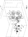
本発明の実施例は、従来技術を表す図1に模式的に示したような半導体ウェーハ・ハンドリングおよび処理装置100である。この装置100は米国特許第4915564号または同第5516732号に図示され説明されている形式の高生産性のカルーセル形式の垂直ウェーハ処理機械10を含み、両特許は本明細書にその記載内容全体を援用される。本発明はまた他の型式のウェーハ処理機械、例えば典型的なクラスター・ツール形式の機械、およびウェーハが全体を通じて水平および上方に向かって配置されて保持される他の機械、ならびにウェーハが他の配向で機械を通して移動または処理される機械にも適用できる。しかしながら、記載された実施例は、特に改造することで本明細書で説明した装置100の形式の機械に特に適している。
【0022】
装置100は二点鎖線で示す框体102を含み、框体は内部にクリーンな雰囲気を収容しており、その中に処理機械10が配置される。框体102は内部に2つのウェーハ・カセット103,104を支持する備えを含んでおり、ウェーハ・カセット103,104は機械10で処理を行うために間隔を隔てて平行な状態で水平に配向されているウェーハ35の垂直スタックを支持するように形成された棚105をそれぞれ含んでいる。ウェーハ・カセット103,104はそれ自体を垂直方向へ移動させる昇降機構106を備えており、棚の各々のウェーハ位置を選択的に移送面へ運び、内部のウェーハ35の取出し、またはカセットの選択した位置への装填ができるようになされている。
【0023】
框体102はまた内部にウェーハ移送機構110を有し、ウェーハ移送機構110はウェーハ移送アーム112を有し、このウェーハ移送アーム112は垂直な枢動軸線115のまわりに回転できると共に、移送面119内を伸長することができる。移送アーム112の自由端には、ウェーハ・カセット103,104に対し、またウェーハ・センタリングまたは整合ステーション118のセンタリング・チャック116および装填アーム60の端部の装填アーム・チャック59に対してウェーハ35のピックアップおよび載置を行うグリップ装置すなわち端部操作具114が備えられている。ウェーハ・カセット103,104、センタリング・チャック116および装填アーム・チャック59は移送アーム112の枢動軸線115のまわりに円形曲線117に沿って位置され、または位置されることができる。装填アーム・チャック59は装填アーム60の長手方向軸線121のまわりに回転して、保持するウェーハ35を、移送アーム112との間のウェーハ移送に必要な水平配向状態と、ウェーハ処理機械10の装填ロック・ステーション14におけるウェーハ・ホルダー30(図2)へ向かう方向および離れる方向のウェーハ移送に必要な垂直配向状態との間で、回転させる。装填アーム60はさらに垂直軸線122のまわりに枢動して、装填ロック・ステーション14におけるウェーハ・ホルダー30へ向かう方向および離れる方向のウェーハ移送を行う。
【0024】
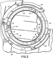
ウェーハ処理機械10は主真空室11を含み、この主真空室11は水平中心軸線19のまわりに等角度に隔てられた複数、例えば5つのステーション14〜18を有する2つのほぼ円形な壁12,13の間に形成されたディスク形の空間とされている。真空室11内には、処理ステーション14〜18の各々と同時に整合するように等間隔に隔てられた5つの円形開口21を有する円形の割出しプレート20が軸線19に回転移動可能に取付けられている。
【0025】
図2に示すように、各開口21内には、割出しプレート20に連結された3つの等角度に隔てられている板ばね28上に弾性的に支持されてシール・リング27が備えられている。各々のシール・リング27内には、3つで1組のセラミックス製の絶縁ピン29上でシール・リング27に対して剛的に支持されてウェーハ・ホルダー30が備えられている。ウェーハ・ホルダー30は、割出しプレート20が5分の1回転、すなわち72゜の角度を割出されたときに各処理ステーション14〜18を通してウェーハ35を運ぶためにそれぞれ備えられている。5つのステーション14〜18のうちの少なくとも1つのステーション、例えばステーション14は装填ロック・ステーションとされ、そのステーションを通してウェーハ35が主真空室11内へ挿入され、また主真空室11から取出される。残りのステーション15〜18は、例えばスパッタ被覆ステーションやエッチング・ステーションのような多数の形式のうちの何れかの処理ステーションとされる。
【0026】
ウェーハ・ホルダー30の各々の主構造は、典型的にはアルミニウムで形成されたリング形の環状本体31である。本体31はクランプ・リング32を有しており、このクランプ・リング32は本体31に対して弾性的に取付けられ、3つで1組の等角度に隔てられた板ばね36によって本体に押圧されている。クランプ・リング32はクランプされるウェーハ35よりも僅かに小さい内径を有する。ウェーハ35は、その周縁の上に位置するクランプ・リング32によって本体31の開口39内に保持される。板ばね36はクランプ・リング32およびウェーハ35を3つで1組のラッチ・クリップ33に押圧するのであり、ラッチ・クリップ33は開口21のまわりに等角度に隔てられた3つのラッチ組立体65のそれぞれの1つである。
【0027】
ラッチ組立体65は多数の形状のうちの何れか1つとされる。図2に示す組立体は、ホルダー本体31のまわりに間隔を隔てて枢動可能に取付けられた、米国特許第5820329号に記載の形式のものである。図2に示すように、ラッチ・クリップ33は一端が枢動軸70の一端に固定され、枢動軸70はホルダー30の本体31を通って延在する軸受(図示せず)内に回転可能に支持される。枢動軸70のクリップ33と反対側の端で、軸は円形ディスク74に剛的に連結されており、円形ディスク74は一対の穴75を有し、円形ディスク74の後方へ向いた面にはフレアーの付いた開口を有する。穴75は軸70の反対両側に同じ距離を隔てられ、装填アーム60のアクチュエータ(図3)のピン62を受入れるようになされて、これによりアクチュエータの回転が円形ディスク74、軸70およびクリップ33を軸70の軸線のまわりに回転させる。軸70の円形ディスク74の回転は90゜の回転移動に制限される。ラッチ組立体65を有するホルダー30の装填では、ウェーハ35はクランプ・リング32に対して押圧されてウェーハ本体31から離すようにそれを移動し、これによりウェーハ33の表面を擦ることなくラッチ・クリップ33はラッチ固定された位置(二点鎖線)とラッチ固定されていない位置(実線)との間で回転できる。
【0028】
代替のラッチ組立体65aが図2Aに示されており、これは本明細書にその記載内容全体を援用される米国特許出願第09/183503号に記載されたものである。ラッチ組立体65aは上述したラッチ組立体65と同様に、ウェーハを保持するクランプ・リング32の開口39のまわりでウェーハ35の周縁をクランプ・リング32に対して押圧する。しかしながら、各ラッチ組立体65aはホルダー本体31に対するよりもクランプ・リング32に対して枢動可能に取付けられる。ラッチ組立体65aはクランプ・リング32に固定されている取付けポスト130に取付けられる。ラッチ組立体65aは、タングステン・カーバイド製ボール軸受(図示せず)を介して取付けポスト130に枢動可能に取付けられている非金属製のラッチ本体131を含み、取付けポスト130を取巻くコイルばね(図示せず)によってクランプ・リング32に押圧される。ラッチ本体131の各々はラッチ組立体65に関連して上述した穴75に似た一対のアクチュエータ・ピン受入れ穴またはスロット175を有し、それらは取付けポスト130から等しく隔てられて移送アームのアクチュエータ機構のアクチュエータ・ピンを受入れるようになされており、以下に説明するようにラッチ組立体65aを作動させる。ラッチ本体131の反対両端には、前部ローラー135および後部ローラー136で構成される一対の非金属製のローラーが回転可能に取付けられている。
【0029】
図3は処理機械10を通り、装填ロック・ステーション14を通る断面図である。
【0030】
装填ロック・ステーション14は移動可能なカップ型の蓋54を含み、この蓋は装填ロック・ステーション14に密閉される装填ロック室55を形成するために、真空室11の前壁12にシール・リング27を押圧するように作動される。扉56は、移送アームまたは装填アーム60の真空チャック59で担持されたウェーハ35へのアクセスを行わせる。
【0031】
半導体デバイスの製造では、装填アーム60はデバイス面を先ず最初にホルダー本体31の開口を通して装填ロック室55内へウェーハ35を移送するように作動し、ウェーハ35の外側リムをクランプ作用するクランプ・リング32の下側に接触させる。デバイス面の処理のために、装填アーム・チャックは円形チャック59aとされ、このチャックはウェーハ35の裏面の中央に係合される。真空チャック59aは装填アーム60の真空ライン69を通して、選択的に作動できる真空源に連結される。
【0032】
ウェーハ上に金のような金属製の連続フィルムを固着させるために裏面の金属処理が実行される場合のように、ウェーハ35の裏面を処理するとき、ウェーハは反転され、チャック59,114,116が装置側からウェーハ35に係合される。チャックとウェーハ上のデバイスとの接触はそれらのデバイスの破損や破壊を防止するために避けねばならないので、ウェーハ35の予定された、すなわち制限された面積部分にデバイスを制限して、ウェーハ表面の除外領域にデバイスが配置されることを避けることが必要である。除外領域は従来よりウェーハ周縁に沿う6mm幅のウェーハの面積部分とされてきた。この除外面積部分では、図3Aに示すように弧状真空チャック59bがウェーハ35の周縁の除外面積部分に対してのみ接触する。チャックのパドルまたはウェーハ係合端部は、ウェーハ周縁に沿う6mm幅のリングの円周の大部分のまわりを延在することが好ましい。
【0033】
ホルダー30に対するウェーハ35の挿入は、ウェーハ35の移動路の外側へラッチ・クリップ33が回転されて行われる。ウェーハ35の後方位置へ、また後方位置からのラッチ・クリップ33の回転は、図3に示されるように、移送アームまたは装填アーム60によって担持されている3つのラッチ・アクチュエータ61で達成される。それぞれのラッチ・アクチュエータ61は空気的に作動される回転式シリンダ63の軸に一対のアクチュエータ・ピン62を含み、ピン62がホルダー30の3つのラッチ組立体65の対応する1つと係合したときに一方向へ90゜回転して、同時に3つのクリップ33をウェーハ35の後方のラッチング位置へ移動させ、また反対方向へ90゜回転してウェーハ35のリムを超えたホルダーの解放位置へクリップ33を移動させる。
【0034】
本発明の基本によれば、装置100のようなウェーハ・ハンドリングおよび処理装置は、図1に関連して説明した装置100のウェーハ移送機構110に類似したウェーハ移送機構210を備えているているが、ウェーハ・ハンドリング・システム200を備えており、図4に一実施例が示されている。システム200は3つのチャックおよび関連するハードウェアを含み、それには移送アーム・チャックまたは上述した移送アーム112のように作動する移送アーム212の端部に配置された端部操作具201が含まれる。システム200はまた、ウェーハ整合ステーション118に上述したセンタリング・チャック116のように作動するセンタリング・チャック216と、上述した装填アーム60のように作動する装填アーム260の端部に一対の装填アーム・チャック259を含む。
【0035】
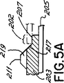
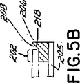
端部操作具201はウェーハ35のデバイス面の周縁の2mm幅の除外領域のみにおいて水平配置されているウェーハ35の下に向いたデバイス面と接触するウェーハ支持面を含む。ウェーハ35は重力の作用で端部操作具201上に係止され、端部操作具201はウェーハ・カセット103,104に向かう方向および離れる方向、整合ステーション118のセンタリング・チャック216に向かう方向および離れる方向、および装填アーム260の装填アーム・チャック259に向かう方向および離れる方向へウェーハ35を移動させるために移動する。図5、図5A〜図5Dは、ねじ204で移送アーム212の端部に固定された移送アーム・プレート203の形態をした本体と、ロッキング・ワッシャ・ナット211で保持されたときに、移送アーム・プレート203の鳩尾形(ダブテール)キー溝(図示せず)に嵌合させてそのプレート203に剛的に取付けられた台形断面の一対のアウトリガー・アーム205とを含む。アウトリガー205は異なる寸法のウェーハを受入れるために、キー溝内で調整できる。アーム205はセラミックス製で、直立した支持先端206を有し、その先端は移送アーム212によって移送されるウェーハ35の除外面積部分202に接触する。プレート203および先端206は除外面積部分202にてウェーハ35を支持するために形成された環状ショルダのセグメント207,208をそれぞれ有する。ショルダ・セグメント207,208に直ぐ隣接して、斜面を有する環状リップの角度間隔を隔てた、すなわち円周方向に隔てられたセグメント217,218がそれぞれ配置され、セグメント217,218は移送アーム212で担持されているウェーハ35の周縁を直接に取囲んでいる。ナット211はセグメント217に対して接線方向に配置され、斜面の付いたリップ伸長部分を形成する円錐ヘッド面219を有して、リップと共にウェーハをショルダ・セグメント207,208へガイドするように作用する。
【0036】
斜面の付いた円周リップのセグメント217,218、およびピン・ヘッド面219は、ウェーハ周縁がリップを超えて係止されず、端部操作具201上の中心の直近にウェーハが支持されるように作用する。斜面の内径は、ウェーハ35の除外領域202の係止される幅が2mmよりも小さいショルダ・セグメント207,208の環状面を取囲む。斜面のこの内径は、標準ウェーハの基準直径、典型的には200mmまたは300mmに、約0.008inすなわち約0.2mmの半径方向の最大公差を加えた寸法に等しく、従って最大ウェーハは斜面の付いた環状リップの内側に係止されることになる。アウトリガー205はワッシャ・ナット211により部分的にプレート202に固定される。ナット211のヘッド219の円錐側面はプレート203の上面よりも上方へセグメント217,218の斜面を伸長して、ウェーハ35がカセット103,104からピックアップされるときに、斜面の付いたリップのセグメント217,218で囲まれる円形面積部分上へウェーハ35をガイドするように助成する。チャックの斜面は、チャックの支持面よりも少なくともウェーハの基準厚さ、好ましくは約1mmほど高く上昇する。斜面の角度は好ましくは約45゜±10゜または±15゜である。斜面はいずれにしても支持面を囲むべきではなく、180゜を超えた範囲にわたる複数点、好ましくは3点以上、好ましくは4点に位置されることができる。ウェーハの取出しおよび交換のために、アウトリガー205はカセット103,104内で重ねられたウェーハ35の間に達するように十分薄くされる。
【0037】
図5に示されるように、アウトリガー205はセンタリング・ステーション118でのセンタリング・チャック216の表面の溝221,222に嵌合する寸法でもある。センタリング・チャック216は低いディスク形の本体216aとセグメントに分けられた直立周縁リング223とを有し、周縁リング223は端部操作具201からウェーハ35を受取るために半円形であり、端部操作具201は、ウェーハ35の平坦部またはノッチ235(図5)をセンタリング・チャック216上の平坦部224と同じ所定の配向になるように移動させるために、ウェーハを上昇および回転させることができる。周縁リング223は移送アーム・チャックの場合と同様に、ウェーハをその除外面積部分内のみでチャックの支持面に接触するようにガイドするために斜面を形成されることができるが、斜面の無い方がセンタリング機構とよりよく共用でき、機能する。図示実施例では、センタリング・ステーションの周縁リング223はウェーハ平面に直角な内面を有する。センタリング・ステーションではセンタリング・チャック216上の光学センサー(図示せず)がウェーハの配向を判定する。
【0038】
同様に図5に示されるように、装填アーム・チャック259の各々は端部操作具201のアウトリガー205を受入れるために溝262,263を有するチャック・プレートまたは本体261を有する。チャック装填アーム・チャック259は図3Aのデバイス面と係合する真空チャック59bに代わる。プレート261はその周縁のまわりにセグメントに分割された直立環状リップ265を有し、その上にウェーハ35の周縁に沿う除外領域が係止される。リップ265は上述した移送アーム・チャックおよびセンタリング・ステーション・チャックの場合と同様に、デバイス面の接触が2mmを超えない幅の除外領域とだけで行われることを保証するために斜面を形成される。
【0039】
図6、図7、図7Aおよび図8に示されるように、リップ265のまわりに間隔を隔てて複数の、例えば2〜4つのグリップ装置またはグリップ・フィンガ270が配置され、各々のグリップ・フィンガは装填アーム・チャック259の本体261に対して軸受で支持されたロッド281に枢動可能に取付けられている。各々のグリップ装置270はウェーハ35の周縁を捕捉するためにノッチ273を有している。各々のグリップ装置270は装填アーム・チャック259に取付けられているアクチュエータ272で制御される作動レバー271を有しており、従来技術のシステムの真空チャック59,59aを作動させるような真空圧制御のためにライン69を通して与えられる真空圧指令に応答して作動するが、それらのチャックは取外されて機械的な装填アーム・チャック259と交換されている。アクチュエータ272は電気的または空気的に制御される空気シリンダ、電気−機械式ソレノイド、または図7および図7Aの解放位置とグリップ位置との間でグリップ装置270を移動させる他のいずれかの装置とされる。さらに、図8に最もよく見られるように、チャック259に適当に装着されたウェーハ35を検出するために、リップ265の一連の穴(図示せず)に連結するために真空ポート295がチャック本体261に備えられる。
【0040】
アクチュエータ272は、装填アーム・チャック259の本体261に固定された本体282と、可動部材283とを有し、グリップ装置270が解放位置となる本体261の近傍の収縮位置(図7)およびグリップ装置270がグリップ位置となる本体261から離れた伸長位置(図7A)の間で可動部材283は本体261に対して直角な方向に往復運動する。アクチュエータ272の可動部材283の端部にアクチュエータ・バー284が固定されており、アクチュエータ・バー284は本体261に平行に延在して可動部材283と共に移動する。各々のグリップ装置270の作動レバー271はフォーク285を有しており、調整可能なセット・スクリュー286が螺合されている。このセット・スクリューは貫通孔287を有し、貫通孔287の中に柔らかなばね288がフック止めされ、このばね288はセット・スクリュー286とアクチュエータ・バー284の遠隔端部との間に緊張状態で連結されている。ばね288は、チャック259のリップ265に対してウェーハ35をクランプするにおいて、グリップ装置270でウェーハ35の裏面に伝えることのできる力の大きさを制限するように機能する。セット・スクリュー286は、この制限が手動調整できるようにするために備えられる。各々の作動レバー271はそこから延在するリンク289も有しており、それらのリンクは互いに遠隔端部において、一方の端部の軸受291上を端部のフォーク290が枢動および滑動するような状態で枢動連結されている。リンク289の端部の相互連結はグリップ装置270の動作を同期させる。
【0041】
グリップ装置270の代わりに、ウェーハを装填アームにラッチ固定するために他の部材を使用できる。例えば、上述で記載し援用した従来技術に関連して説明したようなローラーまたはフィンガを有する回転ラッチが使用できる。これらは空気作動アクチュエータ61または機械的または他の装置で作動できる。
【0042】
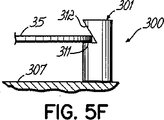
例えば、図5Eは装填アーム・チャック259に対する代替実施例300を示しており、それは1つの固定ピン301および2つのローラー302を含む3つの周縁支持部に対するウェーハ35の支持を使用している。この実施例の装填アーム・チャック300は図5に示した実施例の周縁平坦部235が無く、装填アーム・チャック300mm径のウェーハを支持するために構成された形状で示されている。この代わりに、固定ピン301およびローラー302を省略するために平坦部またはノッチを有するウェーハ35をチャック300上に配置できる。チャック装填アーム・チャック300は装填アーム・チャックまたはセンタリング・ステーション・チャックとして使用できる。チャック300はウェーハ35の周縁上の3以上の点で接触でき、例えばハウジング307を含み、このハウジングに固定ピン301および一対の凹部またはノッチのあるローラー302が取付けられる。ローラー302はウェーハ35の周縁に対してラッチ固定するように、またその周縁から引込められるようにハウジング307に取付けられる。ローラーが引込められた位置にあって固定ピン301に対しているとき、2つのローラー302の間をウェーハ周縁を押し進めることで移送アーム・チャックまたは端部操作具201がウェーハ35をチャック300へ導けるように、チャック300は構成される。ローラー302は固定ピン301からチャック300の中心線303の反対両側に配置されており、ローラーは、少なくとも160゜離されることが好ましいが、180゜未満の離れとされる角度304で隔てられている。160゜未満の角度は、端部操作具201の設計上の理由で受け入れることができない。
【0043】
チャック300が上に向いているとき、例えば図5Fに示されるように2mm幅の除外領域の範囲内でのみウェーハ35と接触してウェーハ35周縁を支持するために、固定ピン301は水平面311を有する。固定ピン301は重なって傾斜したほぼ垂直な面312を有し、この面はウェーハ35の中心へ向かって半径方向内方へ向いている。ローラー302はアクチュエータ61動作に応答してウェーハ35の周縁から離れた引込んだ位置と、図5Eに示されるようにウェーハ35の周縁に対するラッチ固定位置と間を揺動するように、枢動レバー302aに取付けられる。この代わりに、上述で説明した実施例のグリップ・フィンガ270のためのアクチュエータ272の場合のように、真空チャックを制御するために以前使用されていた信号に応答する他のアクチュエータに応答してローラー302が枢動されるようにできる。ローラー302はラッチ固定位置にされたときにウェーハ35の周縁を捕捉するために滑らかな凹面315を有しており、その位置にてウェーハ35は端部操作具201からピックアップされる。ローラー302の凹面315および組合う固定ピン301の傾斜面312および水平面311がチャック300上のウェーハ35を捕捉し、これによりウェーハ35は垂直位置または下方へ向いた配向となるように回転されることができ、またウェーハ・ホルダー30に向かう方向および離れる方向へ移送されることができる。
【0044】
装填アーム・チャックはウェーハ処理機械にウェーハを正しく載置する。このように処理機械の装填ロック室の真空式ウェーハ・ホルダー30内へ位置された後、グリップ装置またはラッチがウェーハを解放すると同時に、ウェーハ・ホルダーがウェーハを把持する。装填ロック室からウェーハを取出すためには、これと逆の手順が使用される。装填アーム・チャックがウェーハ・ホルダーから引出されると、処理機械は次のウェーハ・ホルダーを装填ロック室に割出すことができる。装填アームの2つのチャックにより、装填アームは装填ロック室のウェーハ・ホルダー内にウェーハが存在するかを調べ、存在するならば、そのウェーハを装填アームの空のチャックで取出す。その後、装填アームは180゜回転して新しいウェーハを所定位置に運んで装填ロック室のウェーハ・ホルダー内に装填する。装填ロック室へウェーハを載置したチャックは、その後、装填アームの他方のチャックの処理済みウェーハを端部操作具へ移送するために180゜回転する前に、移送アームの端部操作具から次のウェーハを受取るために使用できる。
【0045】
上述の記載および添付図面は本発明のさまざまな実施例を説明したが、当業者には発明の基本から逸脱することなくさらなる追加および変更が行えることが明白となるであろう。
【図面の簡単な説明】
【図1】 本発明を適用できる従来技術のウェーハ・ハンドリングおよび処理装置を示す斜視図である。
【図1A】 チャック組立体の動作を示す図1の一部分の拡大斜視図である。
【図2】 図1の装置のカルーセル処理機械の従来技術のウェーハ・ホルダーを示す部分的破断図である。
【図2A】 ラッチ固定位置で示される図2のラッチの従来技術の代替実施例を示す詳細図である。
【図3】 従来技術の装置のウェーハ移送アームに関する図1の従来技術の装置のカルーセル処理機械の一部分を通る断面図である。
【図3A】 裏面処理のための従来技術で使用された図3の移送アームの真空チャックの1つの実施例の斜視図である。
【図4】 図1〜図3Aに示した従来技術の装置と共用される本発明の1つの実施例によるウェーハ・ハンドリング・システムの斜視図である。
【図5】 整合ステーションおよび装填アームのウェーハ・チャックと整合された、図4のウェーハ・ハンドリング・システムのウェーハ移送アームの端部操作具の模式的な頂面図である。
【図5A】 図5の線5A−5Aに沿う断面図である。
【図5B】 図5の線5B−5Bに沿う断面図である。
【図5C】 図5の線5C−5Cに沿う断面図である。
【図5D】 図5の線5D−5Dに沿う断面図である。
【図5E】 装填アーム・チャックの他の実施例にウェーハを位置決めするウェーハ移送アームの端部操作具を示す図5に類似の模式的な頂面図である。
【図5F】 図5Eの線5F−5Fに沿う断面図である。
【図5G】 図5Eの線5G−5Gに沿う模式的な断面図である。
【図6】 図5の装填アーム・チャックのグリップ装置の部分的な頂面図である。
【図7】 解放位置での装填アーム・チャックのグリップ装置を示す図6の線7−7に沿う横断面図である。
【図7A】 ウェーハをグリップする装填アーム・チャックのグリップ装置を示す図7に似た断面図である。
【図8】 図7Aの装填アーム・チャックのグリップ装置をさらに詳細に示す拡大した部分的な断面図である。[0001]
The present invention relates to wafer handling, and more particularly to the transfer and holding of semiconductor wafers during semiconductor manufacturing, and further to wafers having a diameter of 200 millimeters (mm) or more.
[0002]
(Background of the Invention)
In the semiconductor industry, many companies manufacture equipment for processing semiconductor wafers, especially silicon wafers, for device manufacturing. Semiconductor wafer processing facilities use automated robotic wafer handling equipment to move wafers through the facility and hold the wafers during processing. Industrial wafer handling equipment typically uses a vacuum chuck, which is equipped with a robotic arm with a vacuum spatula or end-operator that contacts the backside of the wafer. According to a more versatile handling apparatus, contact with the wafer is made in a circular area at the center of the wafer by a vacuum chuck. One such handling device is described in US Pat. No. 5,820,329, the entire contents of which are incorporated herein. The wafer handling is typical in many wafer processing machines for processing wafer device surfaces.
[0003]
In semiconductor manufacturing, when processing of the device side of a wafer is complete, a metal layer is often applied to the back side. In some devices, this metal layer is often gold. Gold backside metal processing and wafer holders for such processing are described in commonly assigned US patent application Ser. No. 09/227911 filed Jan. 8, 1999, which is hereby incorporated herein by reference. The entire description is incorporated in the book. For backside metal processing, processing equipment similar to that used to process the device surface of the wafer is used, but the orientation of the wafer is reversed. Reversing the orientation of the partially processed wafer will expose the device in the center of the wafer so that the vacuum chuck of the wafer transfer arm is in contact. The device usually cannot make such contact without being affected by damage.
[0004]
For this reason, vacuum chucks have been developed to grip the wafer along a 6 mm wide ring inside the periphery of the wafer. As a result, a ring with a width of 6 mm at the periphery of the wafer was left as an excluded area of the wafer that cannot be used for device manufacture. A 6 mm wide exclusion ring is necessary to provide sufficient surface area to ensure that the vacuum chuck can hold the wafer in the vertical, horizontal and reverse orientations required by the handling equipment. Typically, for a 200 mm diameter wafer, the 6 mm wide contact area portion on the wafer that the wafer handling device members engage along the wafer periphery is 36 square centimeters, that is, an area that exceeds 12% of the wafer area. It becomes. It has been said in the industry that it is necessary to reduce the contact area between the wafer and the wafer handling device, preferably no more than 2 mm around the periphery of a wafer having a diameter of 200 mm or 300 mm. The exclusion area of 2 mm width includes an area of about 12 square centimeters for a 200 mm diameter wafer and 18 square centimeters for a 300 mm diameter wafer. This requirement has not been met with the prior art.
[0005]
The wafer handling apparatus operates and is controlled in connection with the operation and control of the machine that it forms part of or interacts with. Fundamental changes in the characteristics and operation of wafer handling equipment, if it occurs, cannot be compatible with the operation and control of semiconductor processing machines and adversely affect them. If changes in wafer handling equipment are not made by machine replacement or redesign, operational software and system operation will be affected.
[0006]
These contact areas typically prevent the use of wafer portions bounded by controlled area portions for device manufacturing and limit the amount of devices per wafer. As the pattern geometry decreases and the demand for increased device volume per wafer increases, the need to increase the effective area of the wafer increases.
[0007]
Accordingly, there is a need for a wafer handling apparatus and wafer handling technology that provides a small contact area or exclusion area that is allowed to contact the wafer. There is also a need for such improved wafer handling that does not affect the operating software and system operation of machines using such improved handling equipment or handling techniques.
[0008]
(Summary of Invention)
A first object of the present invention is to engage and transfer a semiconductor wafer for backside processing while minimizing contact of the wafer with the device surface. A particular object of the present invention is to engage and transfer the semiconductor wafer in contact with the wafer in an exclusion area adjacent to the wafer periphery, particularly in an exclusion area not exceeding 2 mm wide.
[0009]
Another object of the present invention is to provide a method and apparatus for holding and transferring wafers that can hold and transfer different sized wafers, particularly 200 mm and 300 mm diameter wafers that are possible in various dimensions.
[0010]
Another object of the present invention is to hold and transfer wafers that can be shared with, and retrofitted with, the prior art processing machines without the capabilities described above, with reduced device surface contact for wafer backside support. Is to provide a system. A more specific object of the present invention is to provide a modification of the above system to an existing processing machine with minimal impact on the processing machine hardware and little or no impact on the processing machine operating software. is there.
[0011]
In accordance with the basics of the present invention, a wafer transfer that can hold a wafer in contact with a small area of the wafer surface and exchange the wafer between each chuck, wafer cassette and wafer holder of a processing machine. It has an arm chuck, centering station chuck and loading arm chuck, and can contact only the exclusion area, preferably not exceeding about 2 mm width adjacent to the wafer periphery on the device surface of the wafer during backside processing. A wafer handling system is provided.
[0012]
In one embodiment, the transfer arm and load arm wafer chucks have beveled peripheral rings, or peripheral ring segments, having a diameter greater than the diameter of the wafer. The beveled peripheral ring ensures that only a narrow exclusion area at the periphery of the wafer is in contact with the surface on the chuck that supports the wafer. In some applications, the centering station chuck can also include such a beveled peripheral ring.
[0013]
In some embodiments, end controls are provided on the transfer arm. The end manipulator is multi-piece structure to obtain higher flatness, uses internal vacuum channels to determine the presence of the wafer, and accepts different diameter wafers, eg 200 mm and 300 mm diameter For this purpose, it has an adjustable ceramic overhang or outrigger.
[0014]
The centering station chuck corrects the wafer flatness, wafer crystal axis direction and wafer center position. The chuck is preferably a multi-piece structure, using a vacuum channel to detect the presence of the wafer, and using an optical sensor to detect the flat orientation of the wafer as the chuck rotates the wafer. ing. The surface of the alignment station chuck has a recess, such as a gap groove, that allows the outriggers of the end manipulator to place or move the wafer without problems in the window that receives the chuck orientation relative to the home position.
[0015]
The load arm chuck is similar in some respects to the alignment station chuck and interacts with the transfer arm but does not rotate to change the orientation of the wafer. A vacuum channel is used to determine the presence of the wafer. The loading arm has a pivotable wafer periphery hook or grip member that grips the wafer periphery within the exclusion zone. The gripping member is actuated pneumatically with an electro-pneumatic actuator, which responds to the same electrical control signal that activates the vacuum controller, like the vacuum chuck of the previous loading arm. The gripping member of the loading arm chuck is actuated by the movement of the robotic transfer arm relative to the loading arm or the movement of the loading arm relative to the wafer holder of the processing machine. The gripping member may be a pivoting grip hook, or in place of the pivoting grip hook, similar to other types of wafer holding devices, such as latches with the described prior art pivoting rollers or non-contact tabs A rotary latch can be rotated over the wafer periphery to latch the wafer against the loading arm chuck. The gripping member allows the loading arm to hold the wafer vertically or downward and can be held or moved in several other different orientations.
[0016]
In one embodiment of the present invention, a system with a vacuum chuck can replace a vacuum chuck on a mechanical wafer engagement chuck, particularly the transfer arm end manipulator, wafer centering or alignment station, and wafer loading arm. Can be modified. In such a system, the transfer arm is operable to pick up and move horizontally positioned wafers and move them away from or away from the wafer cassette, centering or alignment station, and loading arm. Can be transferred in the direction. The chuck of the centering or alignment station is also operable to receive the wafer from the transfer arm, align and align the wafer, and return the wafer to the central alignment position of the transfer arm in a horizontal alignment state as well. Furthermore, the loading arm chuck moves the wafer between the transfer arm chuck and the wafer holder of the wafer processing machine, or exchanges the wafers with each other, and the horizontal orientation on the transfer arm and the wafer holder of the processing machine. Can be operated to re-orient the wafer between the vertical alignment states at The wafer is held, at least in part, by gravity, on the horizontally oriented and upwardly facing chuck of the transfer arm and alignment station, and horizontally during movement of the arm toward and away from the transfer arm. Partly held by gravity on the loaded arm chuck positioned and up, and positively held by the peripheral grip hook when moved in other orientations.
[0017]
In one embodiment of the present invention, the controller of the wafer handling system can be shared with the controller of a prior art machine with a vacuum chuck, so that the system can be used without substantial hardware changes and The machine can be modified without improving the control software. A vacuum chuck control line is used to detect the presence of a wafer on the chuck. The pneumatic cylinder that operates the gripping device is operated by an electro-pneumatic solenoid that is controlled by an electrical software vacuum command signal provided to operate the vacuum chuck.
[0018]
Embodiments of the present invention can be provided as a retrofit kit, which includes three chuck assemblies configured to replace the existing processing machine transfer arm, alignment station, and loading arm vacuum chuck.
[0019]
The method and apparatus of the present invention increases the effective area of the wafer by about 4%, or from 88% to 96% of the wafer area, reducing the excluded or unusable area of the wafer by two thirds; The average number of devices that can be manufactured per wafer is similarly increased, which provides the benefit of improving semiconductor manufacturing processes and machine productivity.
[0020]
Other objects and advantages of the present invention will become more readily apparent from the following detailed description.
[0021]
(Detailed explanation)
An embodiment of the present invention is a semiconductor wafer handling and
[0022]
The
[0023]
The
[0024]
The
[0025]
As shown in FIG. 2, each opening 21 is provided with a
[0026]
The main structure of each of the
[0027]
The latch assembly 65 is any one of a number of shapes. The assembly shown in FIG. 2 is of the type described in US Pat. No. 5,820,329, which is pivotally mounted about the
[0028]
An
[0029]
FIG. 3 is a cross-sectional view through the processing
[0030]
The
[0031]
In the manufacture of semiconductor devices, the loading arm 60 operates to transfer the
[0032]
When processing the backside of the
[0033]
The insertion of the
[0034]
In accordance with the basics of the present invention, a wafer handling and processing apparatus, such as
[0035]
The
[0036]
The
[0037]
As shown in FIG. 5, the
[0038]
Similarly, as shown in FIG. 5, each of the loading arm chucks 259 has a chuck plate or
[0039]
As shown in FIGS. 6, 7, 7A and 8, a plurality of, for example, two to four gripping devices or
[0040]
The
[0041]
Instead of the
[0042]
For example, FIG. 5E shows an
[0043]
When the
[0044]
The loading arm chuck correctly places the wafer on the wafer processing machine. After being positioned in the
[0045]
While the above description and accompanying drawings illustrate various embodiments of the present invention, it will be apparent to those skilled in the art that further additions and modifications may be made without departing from the basic principles of the invention.
[Brief description of the drawings]
FIG. 1 is a perspective view of a prior art wafer handling and processing apparatus to which the present invention can be applied.
FIG. 1A is an enlarged perspective view of a portion of FIG. 1 illustrating the operation of the chuck assembly.
2 is a partial cutaway view showing a prior art wafer holder of the carousel processing machine of the apparatus of FIG. 1. FIG.
2A is a detailed view of an alternative prior art embodiment of the latch of FIG. 2 shown in the latch lock position. FIG.
FIG. 3 is a cross-sectional view through a portion of the carousel processing machine of the prior art apparatus of FIG. 1 with respect to the wafer transfer arm of the prior art apparatus.
3A is a perspective view of one embodiment of a vacuum chuck of the transfer arm of FIG. 3 used in the prior art for backside processing. FIG.
4 is a perspective view of a wafer handling system according to one embodiment of the present invention shared with the prior art apparatus shown in FIGS. 1-3A. FIG.
5 is a schematic top view of an end manipulator of a wafer transfer arm of the wafer handling system of FIG. 4 aligned with an alignment station and a wafer chuck of a loading arm. FIG.
5A is a cross-sectional view taken along
5B is a cross-sectional view taken along line 5B-5B in FIG.
5C is a cross-sectional view taken along
5D is a cross-sectional view taken along
5E is a schematic top view similar to FIG. 5 showing the wafer transfer arm end manipulator positioning the wafer in another embodiment of the loading arm chuck. FIG.
5F is a cross-sectional view taken along
5G is a schematic cross-sectional view taken along
FIG. 6 is a partial top view of the gripping device of the loading arm chuck of FIG.
7 is a cross-sectional view taken along line 7-7 of FIG. 6 showing the gripping device of the loading arm chuck in the release position.
7A is a cross-sectional view similar to FIG. 7 showing a gripping device for a loading arm chuck for gripping a wafer. FIG.
8 is an enlarged partial cross-sectional view showing the loading arm chuck gripping device of FIG. 7A in more detail. FIG.
Claims (24)
Applications Claiming Priority (2)
| Application Number | Priority Date | Filing Date | Title |
|---|---|---|---|
| US09/725,823 US6692219B2 (en) | 2000-11-29 | 2000-11-29 | Reduced edge contact wafer handling system and method of retrofitting and using same |
| PCT/US2002/001545 WO2002045137A2 (en) | 2000-11-29 | 2001-11-20 | Reduced edge contact wafer handling system and method of retrofitting and using same |
Publications (3)
| Publication Number | Publication Date |
|---|---|
| JP2004515073A JP2004515073A (en) | 2004-05-20 |
| JP2004515073A5 JP2004515073A5 (en) | 2005-05-26 |
| JP4060185B2 true JP4060185B2 (en) | 2008-03-12 |
Family
ID=24916099
Family Applications (1)
| Application Number | Title | Priority Date | Filing Date |
|---|---|---|---|
| JP2002547208A Expired - Lifetime JP4060185B2 (en) | 2000-11-29 | 2001-11-20 | Wafer handling system with reduced edge contact, modification method and use thereof |
Country Status (7)
| Country | Link |
|---|---|
| US (1) | US6692219B2 (en) |
| EP (1) | EP1340246A2 (en) |
| JP (1) | JP4060185B2 (en) |
| CN (1) | CN1481577A (en) |
| AU (1) | AU2002236801A1 (en) |
| TW (1) | TW511136B (en) |
| WO (1) | WO2002045137A2 (en) |
Cited By (1)
| Publication number | Priority date | Publication date | Assignee | Title |
|---|---|---|---|---|
| US11251066B2 (en) | 2018-05-17 | 2022-02-15 | Semes Co., Ltd. | Transfer unit and substrate processing apparatus including the same |
Families Citing this family (52)
| Publication number | Priority date | Publication date | Assignee | Title |
|---|---|---|---|---|
| US6986636B2 (en) * | 2000-06-09 | 2006-01-17 | Brooks Automation, Inc. | Device for positioning disk-shaped objects |
| US6824343B2 (en) * | 2002-02-22 | 2004-11-30 | Applied Materials, Inc. | Substrate support |
| DE10217028C1 (en) * | 2002-04-11 | 2003-11-20 | Nanophotonics Ag | Measuring module for wafer production plants |
| EP1534616A4 (en) * | 2002-06-14 | 2010-04-28 | Fortrend Engineering Corp | Universal reticle transfer system |
| US6769861B2 (en) * | 2002-10-08 | 2004-08-03 | Brooks Automation Inc. | Apparatus for alignment and orientation of a wafer for processing |
| SG115602A1 (en) * | 2003-01-09 | 2005-10-28 | Disco Corp | Conveying device for a plate-like workpiece |
| JP3981885B2 (en) * | 2003-05-20 | 2007-09-26 | 株式会社ダイフク | Transport device |
| US7654596B2 (en) * | 2003-06-27 | 2010-02-02 | Mattson Technology, Inc. | Endeffectors for handling semiconductor wafers |
| TW200532043A (en) * | 2004-02-10 | 2005-10-01 | Ulvac Inc | Thin film forming apparatus |
| US6833717B1 (en) * | 2004-02-12 | 2004-12-21 | Applied Materials, Inc. | Electron beam test system with integrated substrate transfer module |
| US8668422B2 (en) * | 2004-08-17 | 2014-03-11 | Mattson Technology, Inc. | Low cost high throughput processing platform |
| US7798764B2 (en) | 2005-12-22 | 2010-09-21 | Applied Materials, Inc. | Substrate processing sequence in a cartesian robot cluster tool |
| US7651306B2 (en) * | 2004-12-22 | 2010-01-26 | Applied Materials, Inc. | Cartesian robot cluster tool architecture |
| US20060130767A1 (en) * | 2004-12-22 | 2006-06-22 | Applied Materials, Inc. | Purged vacuum chuck with proximity pins |
| US7819079B2 (en) * | 2004-12-22 | 2010-10-26 | Applied Materials, Inc. | Cartesian cluster tool configuration for lithography type processes |
| US20060182535A1 (en) * | 2004-12-22 | 2006-08-17 | Mike Rice | Cartesian robot design |
| US8167522B2 (en) * | 2005-03-30 | 2012-05-01 | Brooks Automation, Inc. | Substrate transport apparatus with active edge gripper |
| US7374391B2 (en) * | 2005-12-22 | 2008-05-20 | Applied Materials, Inc. | Substrate gripper for a substrate handling robot |
| JP4636288B2 (en) * | 2005-05-18 | 2011-02-23 | 株式会社村田製作所 | Positioning stage, bump forming apparatus and bump forming method using the same |
| WO2007008555A2 (en) * | 2005-07-08 | 2007-01-18 | Asyst Technologies, Inc. | Workpiece support structures and apparatus for accessing same |
| KR100631928B1 (en) * | 2005-12-02 | 2006-10-04 | 삼성전자주식회사 | Wafer guide in wafer cleaning apparatus |
| US20070231108A1 (en) * | 2006-04-04 | 2007-10-04 | Applied Materials, Inc. | Method and apparatus for transferring wafers |
| KR100809594B1 (en) * | 2006-09-12 | 2008-03-04 | 세메스 주식회사 | Chucking member and spin head, method for chucking a substrate using the chucking member |
| CN101563769B (en) * | 2006-12-14 | 2012-07-18 | 凯思捷股份有限公司 | Disc holding apparatus and defect/foreign material detecting apparatus |
| US20080166210A1 (en) * | 2007-01-05 | 2008-07-10 | Applied Materials, Inc. | Supinating cartesian robot blade |
| US7694688B2 (en) | 2007-01-05 | 2010-04-13 | Applied Materials, Inc. | Wet clean system design |
| WO2008133149A1 (en) * | 2007-04-23 | 2008-11-06 | Ulvac, Inc. | Supporting member, carrier and supporting method |
| JP5206528B2 (en) * | 2009-03-19 | 2013-06-12 | トヨタ自動車株式会社 | Work conveying device and work conveying method |
| US8698099B2 (en) * | 2009-09-30 | 2014-04-15 | Kyocera Corporation | Attraction member, and attraction device and charged particle beam apparatus using the same |
| US9859141B2 (en) | 2010-04-15 | 2018-01-02 | Suss Microtec Lithography Gmbh | Apparatus and method for aligning and centering wafers |
| US9837295B2 (en) | 2010-04-15 | 2017-12-05 | Suss Microtec Lithography Gmbh | Apparatus and method for semiconductor wafer leveling, force balancing and contact sensing |
| JP5574177B2 (en) * | 2010-09-16 | 2014-08-20 | 株式会社ダイフク | Transport device |
| TWI579939B (en) * | 2011-08-04 | 2017-04-21 | 政美應用股份有限公司 | Device and method for testing and classifying led wafer |
| JP5877016B2 (en) * | 2011-08-26 | 2016-03-02 | 株式会社Screenホールディングス | Substrate reversing apparatus and substrate processing apparatus |
| US8556566B1 (en) * | 2011-09-30 | 2013-10-15 | WD Media, LLC | Disk stacking method and apparatus |
| US9136155B2 (en) * | 2011-11-17 | 2015-09-15 | Lam Research Ag | Method and device for processing wafer shaped articles |
| DE102012100825A1 (en) * | 2011-12-01 | 2013-06-06 | solar-semi GmbH | Apparatus for processing a substrate and method therefor |
| US9431282B2 (en) * | 2011-12-27 | 2016-08-30 | Rudolph Technologies, Inc. | Wafer inversion mechanism |
| US20140064888A1 (en) * | 2012-09-06 | 2014-03-06 | Texas Instruments Incorporated | Appartaus for handling an electronic device and related methodology |
| CN102903661A (en) * | 2012-10-25 | 2013-01-30 | 上海宏力半导体制造有限公司 | Wafer tail end executor |
| JP6186124B2 (en) * | 2012-12-14 | 2017-08-23 | 東京応化工業株式会社 | Transfer arm, transfer device, and transfer method |
| WO2015158390A1 (en) * | 2014-04-17 | 2015-10-22 | Applied Materials, Inc. | Carrier for substrates |
| US9410249B2 (en) * | 2014-05-15 | 2016-08-09 | Infineon Technologies Ag | Wafer releasing |
| US10293365B2 (en) * | 2014-09-18 | 2019-05-21 | Halliburton Energy Services, Inc. | Electrically conductive pattern printer for downhole tools |
| CN105619406B (en) * | 2015-12-31 | 2017-10-17 | 北京七星华创电子股份有限公司 | The calibration method of multifinger mechanical handsheet fork |
| USD803283S1 (en) | 2016-05-16 | 2017-11-21 | Veeco Instruments Inc. | Wafer handling assembly |
| TWI766105B (en) | 2017-09-28 | 2022-06-01 | 美商魯道夫科技股份有限公司 | Wafer-level package assembly handling |
| US11121019B2 (en) * | 2018-06-19 | 2021-09-14 | Kla Corporation | Slotted electrostatic chuck |
| TW202038370A (en) * | 2019-03-13 | 2020-10-16 | 以色列商核心流有限公司 | Circular wafer lateral positioning device |
| CN111392395A (en) * | 2020-03-30 | 2020-07-10 | 武汉华星光电半导体显示技术有限公司 | Feeding device |
| JP7005690B2 (en) * | 2020-06-17 | 2022-02-10 | 株式会社Kokusai Electric | Substrate processing equipment, semiconductor device manufacturing methods, and programs |
| CN112858343B (en) * | 2021-02-02 | 2021-11-16 | 西安中科微星光电科技有限公司 | Multifunctional silicon-based liquid crystal chip online detection system and method |
Family Cites Families (19)
| Publication number | Priority date | Publication date | Assignee | Title |
|---|---|---|---|---|
| US4915564A (en) | 1986-04-04 | 1990-04-10 | Materials Research Corporation | Method and apparatus for handling and processing wafer-like materials |
| US5749469A (en) * | 1992-05-15 | 1998-05-12 | Fluoroware, Inc. | Wafer carrier |
| US5516732A (en) | 1992-12-04 | 1996-05-14 | Sony Corporation | Wafer processing machine vacuum front end method and apparatus |
| JP3143770B2 (en) * | 1994-10-07 | 2001-03-07 | 東京エレクトロン株式会社 | Substrate transfer device |
| US5700046A (en) * | 1995-09-13 | 1997-12-23 | Silicon Valley Group, Inc. | Wafer gripper |
| US5647626A (en) * | 1995-12-04 | 1997-07-15 | Taiwan Semiconductor Manufacturing Company, Ltd. | Wafer pickup system |
| US5746460A (en) * | 1995-12-08 | 1998-05-05 | Applied Materials, Inc. | End effector for semiconductor wafer transfer device and method of moving a wafer with an end effector |
| TW321192U (en) * | 1995-12-23 | 1997-11-21 | Samsung Electronics Co Ltd | A arm of robot for transporting semiconductor wafer |
| US5980194A (en) * | 1996-07-15 | 1999-11-09 | Applied Materials, Inc. | Wafer position error detection and correction system |
| US5820329A (en) | 1997-04-10 | 1998-10-13 | Tokyo Electron Limited | Vacuum processing apparatus with low particle generating wafer clamp |
| JP2001522142A (en) | 1997-11-03 | 2001-11-13 | エーエスエム アメリカ インコーポレイテッド | Improved low mass wafer support system |
| US6116848A (en) * | 1997-11-26 | 2000-09-12 | Brooks Automation, Inc. | Apparatus and method for high-speed transfer and centering of wafer substrates |
| WO1999043021A1 (en) * | 1998-02-18 | 1999-08-26 | Applied Materials, Inc. | End effector for wafer handler in processing system |
| EP1112220A1 (en) | 1998-07-11 | 2001-07-04 | Semitool, Inc. | Robots for microelectronic workpiece handling |
| DE59914581D1 (en) | 1998-09-02 | 2008-01-24 | Tec Sem Ag | DEVICE AND METHOD FOR HANDLING INDIVIDUAL WAFERS |
| US6298280B1 (en) * | 1998-09-28 | 2001-10-02 | Asyst Technologies, Inc. | Method for in-cassette wafer center determination |
| US6143147A (en) | 1998-10-30 | 2000-11-07 | Tokyo Electron Limited | Wafer holding assembly and wafer processing apparatus having said assembly |
| JP2000260859A (en) | 1999-03-09 | 2000-09-22 | Nikon Corp | Substrate housing device |
| US6357996B2 (en) * | 1999-05-14 | 2002-03-19 | Newport Corporation | Edge gripping specimen prealigner |
-
2000
- 2000-11-29 US US09/725,823 patent/US6692219B2/en not_active Expired - Lifetime
-
2001
- 2001-11-16 TW TW090128565A patent/TW511136B/en not_active IP Right Cessation
- 2001-11-20 AU AU2002236801A patent/AU2002236801A1/en not_active Abandoned
- 2001-11-20 JP JP2002547208A patent/JP4060185B2/en not_active Expired - Lifetime
- 2001-11-20 WO PCT/US2002/001545 patent/WO2002045137A2/en not_active Application Discontinuation
- 2001-11-20 EP EP02703165A patent/EP1340246A2/en not_active Withdrawn
- 2001-11-20 CN CNA018199429A patent/CN1481577A/en active Pending
Cited By (1)
| Publication number | Priority date | Publication date | Assignee | Title |
|---|---|---|---|---|
| US11251066B2 (en) | 2018-05-17 | 2022-02-15 | Semes Co., Ltd. | Transfer unit and substrate processing apparatus including the same |
Also Published As
| Publication number | Publication date |
|---|---|
| CN1481577A (en) | 2004-03-10 |
| TW511136B (en) | 2002-11-21 |
| AU2002236801A1 (en) | 2002-06-11 |
| JP2004515073A (en) | 2004-05-20 |
| US6692219B2 (en) | 2004-02-17 |
| WO2002045137A2 (en) | 2002-06-06 |
| US20020064450A1 (en) | 2002-05-30 |
| WO2002045137A3 (en) | 2003-03-20 |
| EP1340246A2 (en) | 2003-09-03 |
Similar Documents
| Publication | Publication Date | Title |
|---|---|---|
| JP4060185B2 (en) | Wafer handling system with reduced edge contact, modification method and use thereof | |
| US6612590B2 (en) | Apparatus and methods for manipulating semiconductor wafers | |
| US6361648B1 (en) | Wafer transfer station for a chemical mechanical polisher | |
| US6174011B1 (en) | Method of and apparatus for handling thin and flat workpieces and the like | |
| US5820329A (en) | Vacuum processing apparatus with low particle generating wafer clamp | |
| KR100281257B1 (en) | Wafer transport module with a rotatable and horizontally extendable wafer holder | |
| US6729462B2 (en) | Edge grip aligner with buffering capabilities | |
| JP2004515073A5 (en) | ||
| US20060157998A1 (en) | Contamination-free edge gripping mechanism and method for loading/unloading and transferring flat objects | |
| JP2010258480A (en) | Aligner apparatus | |
| US20070018469A1 (en) | Contamination-free edge gripping mechanism with withdrawable pads and method for loading/unloading and transferring flat objects | |
| EP1866958B1 (en) | High speed substrate aligner apparatus | |
| JP2002520860A (en) | Wafer carrier and method for handling wafers with minimal contact | |
| JP2022160683A5 (en) | ||
| US6040585A (en) | Method for detecting wafer orientation during transport | |
| US5931627A (en) | Wafer transport apparatus that can transfer multiple wafers in a short period of time | |
| JPH01281744A (en) | Etching device | |
| CN114300397A (en) | Mechanical arm for transmitting wafer and transmission device | |
| GB2146557A (en) | Centering device | |
| JP2002307343A (en) | Method and device for transferring sheet material | |
| TW202306015A (en) | Wafer transfer device, vapor deposition system and use method thereof preventing the upper surface of the undeposited wafer from being polluted by contact | |
| JPS62141731A (en) | Wafer handling apparatus | |
| JPS62141732A (en) | Wafer handling apparatus | |
| KR20000028401A (en) | Wafer loading apparatus of semiconductor manufacturing equipment | |
| JPS62122232A (en) | Mounting device |
Legal Events
| Date | Code | Title | Description |
|---|---|---|---|
| A131 | Notification of reasons for refusal |
Free format text: JAPANESE INTERMEDIATE CODE: A131 Effective date: 20070703 |
|
| A601 | Written request for extension of time |
Free format text: JAPANESE INTERMEDIATE CODE: A601 Effective date: 20071003 |
|
| A602 | Written permission of extension of time |
Free format text: JAPANESE INTERMEDIATE CODE: A602 Effective date: 20071011 |
|
| A521 | Request for written amendment filed |
Free format text: JAPANESE INTERMEDIATE CODE: A523 Effective date: 20071030 |
|
| TRDD | Decision of grant or rejection written | ||
| A01 | Written decision to grant a patent or to grant a registration (utility model) |
Free format text: JAPANESE INTERMEDIATE CODE: A01 Effective date: 20071127 |
|
| A61 | First payment of annual fees (during grant procedure) |
Free format text: JAPANESE INTERMEDIATE CODE: A61 Effective date: 20071219 |
|
| FPAY | Renewal fee payment (event date is renewal date of database) |
Free format text: PAYMENT UNTIL: 20101228 Year of fee payment: 3 |
|
| R150 | Certificate of patent or registration of utility model |
Free format text: JAPANESE INTERMEDIATE CODE: R150 Ref document number: 4060185 Country of ref document: JP Free format text: JAPANESE INTERMEDIATE CODE: R150 |
|
| FPAY | Renewal fee payment (event date is renewal date of database) |
Free format text: PAYMENT UNTIL: 20101228 Year of fee payment: 3 |
|
| FPAY | Renewal fee payment (event date is renewal date of database) |
Free format text: PAYMENT UNTIL: 20131228 Year of fee payment: 6 |
|
| R250 | Receipt of annual fees |
Free format text: JAPANESE INTERMEDIATE CODE: R250 |
|
| R250 | Receipt of annual fees |
Free format text: JAPANESE INTERMEDIATE CODE: R250 |
|
| R250 | Receipt of annual fees |
Free format text: JAPANESE INTERMEDIATE CODE: R250 |
|
| R250 | Receipt of annual fees |
Free format text: JAPANESE INTERMEDIATE CODE: R250 |
|
| R250 | Receipt of annual fees |
Free format text: JAPANESE INTERMEDIATE CODE: R250 |
|
| EXPY | Cancellation because of completion of term |