JP4051568B2 - Component mounting board inspection equipment - Google Patents
Component mounting board inspection equipment Download PDFInfo
- Publication number
- JP4051568B2 JP4051568B2 JP2004032567A JP2004032567A JP4051568B2 JP 4051568 B2 JP4051568 B2 JP 4051568B2 JP 2004032567 A JP2004032567 A JP 2004032567A JP 2004032567 A JP2004032567 A JP 2004032567A JP 4051568 B2 JP4051568 B2 JP 4051568B2
- Authority
- JP
- Japan
- Prior art keywords
- component mounting
- mounting board
- distance
- solder bridge
- electrode pads
- Prior art date
- Legal status (The legal status is an assumption and is not a legal conclusion. Google has not performed a legal analysis and makes no representation as to the accuracy of the status listed.)
- Expired - Fee Related
Links
Images


Classifications
-
- G—PHYSICS
- G06—COMPUTING; CALCULATING OR COUNTING
- G06T—IMAGE DATA PROCESSING OR GENERATION, IN GENERAL
- G06T7/00—Image analysis
- G06T7/0002—Inspection of images, e.g. flaw detection
- G06T7/0004—Industrial image inspection
- G06T7/0006—Industrial image inspection using a design-rule based approach
-
- G—PHYSICS
- G01—MEASURING; TESTING
- G01B—MEASURING LENGTH, THICKNESS OR SIMILAR LINEAR DIMENSIONS; MEASURING ANGLES; MEASURING AREAS; MEASURING IRREGULARITIES OF SURFACES OR CONTOURS
- G01B11/00—Measuring arrangements characterised by the use of optical techniques
- G01B11/14—Measuring arrangements characterised by the use of optical techniques for measuring distance or clearance between spaced objects or spaced apertures
-
- G—PHYSICS
- G01—MEASURING; TESTING
- G01N—INVESTIGATING OR ANALYSING MATERIALS BY DETERMINING THEIR CHEMICAL OR PHYSICAL PROPERTIES
- G01N21/00—Investigating or analysing materials by the use of optical means, i.e. using sub-millimetre waves, infrared, visible or ultraviolet light
- G01N21/84—Systems specially adapted for particular applications
- G01N21/88—Investigating the presence of flaws or contamination
- G01N21/95—Investigating the presence of flaws or contamination characterised by the material or shape of the object to be examined
- G01N21/956—Inspecting patterns on the surface of objects
- G01N21/95684—Patterns showing highly reflecting parts, e.g. metallic elements
-
- G—PHYSICS
- G01—MEASURING; TESTING
- G01N—INVESTIGATING OR ANALYSING MATERIALS BY DETERMINING THEIR CHEMICAL OR PHYSICAL PROPERTIES
- G01N21/00—Investigating or analysing materials by the use of optical means, i.e. using sub-millimetre waves, infrared, visible or ultraviolet light
- G01N21/84—Systems specially adapted for particular applications
- G01N21/88—Investigating the presence of flaws or contamination
- G01N21/95—Investigating the presence of flaws or contamination characterised by the material or shape of the object to be examined
- G01N21/956—Inspecting patterns on the surface of objects
- G01N2021/95638—Inspecting patterns on the surface of objects for PCB's
- G01N2021/95646—Soldering
-
- G—PHYSICS
- G06—COMPUTING; CALCULATING OR COUNTING
- G06T—IMAGE DATA PROCESSING OR GENERATION, IN GENERAL
- G06T2207/00—Indexing scheme for image analysis or image enhancement
- G06T2207/30—Subject of image; Context of image processing
- G06T2207/30108—Industrial image inspection
- G06T2207/30141—Printed circuit board [PCB]
-
- G—PHYSICS
- G06—COMPUTING; CALCULATING OR COUNTING
- G06T—IMAGE DATA PROCESSING OR GENERATION, IN GENERAL
- G06T2207/00—Indexing scheme for image analysis or image enhancement
- G06T2207/30—Subject of image; Context of image processing
- G06T2207/30108—Industrial image inspection
- G06T2207/30152—Solder
-
- H—ELECTRICITY
- H05—ELECTRIC TECHNIQUES NOT OTHERWISE PROVIDED FOR
- H05K—PRINTED CIRCUITS; CASINGS OR CONSTRUCTIONAL DETAILS OF ELECTRIC APPARATUS; MANUFACTURE OF ASSEMBLAGES OF ELECTRICAL COMPONENTS
- H05K1/00—Printed circuits
- H05K1/02—Details
- H05K1/0266—Marks, test patterns or identification means
- H05K1/0269—Marks, test patterns or identification means for visual or optical inspection
-
- H—ELECTRICITY
- H05—ELECTRIC TECHNIQUES NOT OTHERWISE PROVIDED FOR
- H05K—PRINTED CIRCUITS; CASINGS OR CONSTRUCTIONAL DETAILS OF ELECTRIC APPARATUS; MANUFACTURE OF ASSEMBLAGES OF ELECTRICAL COMPONENTS
- H05K3/00—Apparatus or processes for manufacturing printed circuits
- H05K3/30—Assembling printed circuits with electric components, e.g. with resistor
- H05K3/32—Assembling printed circuits with electric components, e.g. with resistor electrically connecting electric components or wires to printed circuits
- H05K3/34—Assembling printed circuits with electric components, e.g. with resistor electrically connecting electric components or wires to printed circuits by soldering
- H05K3/3457—Solder materials or compositions; Methods of application thereof
- H05K3/3485—Applying solder paste, slurry or powder
Description
本発明は、部品実装基板の電極パッド上に印刷されたクリーム半田の良否を検査する、特に隣接する電極パッド間に半田ブリッジが生じているか否かを検査する部品実装基板検査装置に関するものである。 The present invention relates to a component mounting board inspection apparatus that inspects the quality of cream solder printed on electrode pads of a component mounting board, and in particular, checks whether a solder bridge is formed between adjacent electrode pads. .
半導体装置などの部品を多数実装するためのプリント基板などの部品実装基板には、それら部品の電極数に対応した多数の電極パッドと配線回路パターンが形成されており、それら部品を半田付けするために、前記電極パッド上にスクリーン印刷法などによりクリーム半田が印刷されている。このクリーム半田が電極パッド上に良好に印刷されていない場合には部品を良好に半田付けできない。従って、部品実装基板上に部品を半田付けする前に、前記クリーム半田が各電極パッド上に良好に印刷されているか否かを部品実装基板検査装置を用いて検査している。 A component mounting board such as a printed circuit board for mounting a large number of components such as semiconductor devices has a large number of electrode pads and wiring circuit patterns corresponding to the number of electrodes of those components, and soldering these components. Furthermore, cream solder is printed on the electrode pads by a screen printing method or the like. If this cream solder is not printed well on the electrode pads, the parts cannot be soldered well. Therefore, before soldering the component onto the component mounting board, it is inspected by using the component mounting board inspection apparatus whether or not the cream solder is well printed on each electrode pad.
その部品実装基板検査装置の機能ブロック図を図4に示した。図4において、符号100は部品実装基板検査装置を指す。この部品実装基板検査装置100は円環状の照明装置110、CCDカメラのようなカメラ120、画像処理装置130、制御装置140、結果表示装置150などを備えている。
The functional block diagram of the component mounting board inspection apparatus is shown in FIG. In FIG. 4, reference numeral 100 denotes a component mounting board inspection apparatus. The component mounting board inspection apparatus 100 includes an
照明装置110は部品実装基板Bを見やすくする手段であり、カメラ120は照明装置110で照明された部品実装基板Bの外観画像を取り込む手段であり、画像処理装置130は、カメラ120から出力された画像を取り込み、検査アルゴリズムを実行する手段であり、制御装置140は照明装置110の照明の明るさや照明装置110及びカメラ120の駆動を制御する手段であり、結果表示装置150は得られた検査結果を表示する手段である。
The
クリーム半田の印刷の良否の判定手法は、部品実装基板検査装置100に予め設定しているクリーム半田の印刷の情報(クリーム半田の印刷面積、クリーム半田の印刷幅、クリーム半田の印刷の位置)を基に部品実装基板B上のクリーム半田の印刷状態を画像処理装置130を用いて取り込まれた情報と比較処理することでクリーム半田の印刷の良否の判定を行う。
The determination method of the quality of cream solder printing is based on cream solder printing information (cream solder printing area, cream solder printing width, cream solder printing position) preset in the component mounting board inspection apparatus 100. Based on the comparison processing of the printing state of the cream solder on the component mounting board B with the information taken in using the
このようなクリーム半田の検査方法は、被検査物体がクリーム半田ではなく、リフローを行った後の半田であって、その検査ではあるが、特許文献1で公開されている。
Such an inspection method for cream solder is not cream cream solder but solder after reflowing, and this inspection is disclosed in
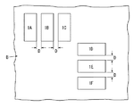
前記部品実装基板Bには各種の半導体装置を始めとして各種の部品を実装できるように各種の電極パッドが形成されている。部品実装基板B上には、図5に一部分を示したように、所定の配列で複数の電極パッド1A、1B、1C・・・が形成されており、それらの電極パッドのパッド間距離は広い所もあれば狭いところもある(パッド間距離の広い電極パッドは図示していない)。図5に示したように、例えば、BGA(Ball Grid Arrayの略)型ICやQFP(Quad Flat Packageの略)型ICを実装する電極パッド1A、1B、1C・・・のパッド間距離Dは極めて狭く、例えば、500μm程度或いはこれ以下と狭い。これらの電極パッド1A、1B、1C・・・上にクリーム半田Sをスクリーン印刷法などで印刷した場合、図6に示したように、電極パッド1Bからはみ出さないようにクリーム半田Sが印刷されることが望ましいが、図7に示したように、或る電極パッド、例えば、電極パッド1A上のクリーム半田Sが右側に隣接する電極パッド1Bに掛かる、いわゆる半田ブリッジSbが発生することがある。無論、このような半田ブリッジSbの発生は好ましくなく、これを確実に検出して、半田ブリッジSbが発生している部品実装基板Bはラインから除去しなければならない。
Various electrode pads are formed on the component mounting board B so that various components including various semiconductor devices can be mounted. As shown in part in FIG. 5, a plurality of
従来、このような半田ブリッジSbを検出するための検査プログラム作成では、オペレータが、半田ブリッジSbが発生しそうなパッド間に、電極パッド1A、1B、1C・・・を見る検査ポイントPaに隣接する電極パッドまで広げた、点線で示したブリッジ検査ポイントPbを手動で設定していた。なお、パッド間距離Dが広い電極パッド間には半田ブリッジ検査ポイントPbを設ける必要はなく、各電極パッド上のクリーム半田Sの状態を見る検査ポイントPaのみでよい。
従って、オペレータが手動設定をしないで検査を行った場合、半田ブリッジによる不良にも係わらず、別の不良としての検出や見逃しが起きていた。 Therefore, when the operator performs an inspection without manual setting, detection as a different defect or an oversight has occurred despite the defect caused by the solder bridge.
また、半田ブリッジ検査対象領域に対しては、前記のように個別に検査ポイントPbを教示しなければならなかったり、検査ポイントPbは部品実装基板B上の同一パターンにのみ展開(コピー)が可能といった制約があった。このため半田ブリッジ検査領域(検査ポイント)Pbを指定したデータの作成に非常に多くの時間を要していた。 Further, as described above, the inspection point Pb must be individually taught for the solder bridge inspection target area, or the inspection point Pb can be developed (copied) only in the same pattern on the component mounting board B. There were restrictions such as. For this reason, it takes a very long time to create data specifying the solder bridge inspection area (inspection point) Pb.
本発明は、これらの課題を解決しようとするものであって、半田ブリッジ検査領域(検査ポイント)を自動で設定でき、最適な検査結果の半田ブリッジを出力することができる実装基板検査装置を得ることを目的とする。 The present invention is intended to solve these problems, and provides a mounting board inspection apparatus capable of automatically setting a solder bridge inspection region (inspection point) and outputting a solder bridge having an optimum inspection result. For the purpose.
本発明の部品実装基板検査装置は、複数の電極パッドが所定の間隔で形成されている部品実装基板を照明する照明手段と、照明された前記部品実装基板を撮影し、画像データを出力するカメラ手段と、前記画像データを2値化する2値化手段と、前記2値化された画像を記憶する2値化画像記憶手段と、前記記憶された2値化画像から前記各電極パッドの位置座標を取得する位置座標取得手段と、前記各電極パッドの位置座標から隣接する電極パッドのパッド間距離を測定する近傍距離測定手段と、前記各パッド間距離を人為的に設定されたしきい値と比較する比較手段と、前記パッド間距離が前記しきい値より狭い場合に半田ブリッジ検査ポイントを設定する半田ブリッジ検査ポイント設定手段とを備えていることを特徴とする。 An apparatus for inspecting a component mounting board according to the present invention includes a lighting unit that illuminates a component mounting board in which a plurality of electrode pads are formed at predetermined intervals, and a camera that photographs the illuminated component mounting board and outputs image data. Means, binarizing means for binarizing the image data, binarized image storage means for storing the binarized image, and the position of each electrode pad from the stored binarized image Position coordinate acquisition means for acquiring coordinates, proximity distance measurement means for measuring a distance between adjacent electrode pads from the position coordinates of each electrode pad, and a threshold value for which the distance between each pad is set artificially And a comparison means for comparing and a solder bridge inspection point setting means for setting a solder bridge inspection point when the distance between the pads is smaller than the threshold value.
従って、本発明の部品実装基板検査装置によれば、半田ブリッジ検査ポイント(領域)を自動で設定することができ、このことにより、オペレータは手動設定する手間と時間を掛けずに最適な検査結果を出力することができる。 Therefore, according to the component mounting board inspection apparatus of the present invention, it is possible to automatically set the solder bridge inspection point (area), which makes it possible for the operator to set the optimum inspection result without taking time and effort for manual setting. Can be output.
また、今後、一層複雑化が予想される様々な部品実装基板においても、しきい値の設定のみで半田ブリッジ検査ポイント(領域)を最適に設定できる。 In addition, in various component mounting boards that are expected to become more complicated in the future, it is possible to optimally set the solder bridge inspection point (area) only by setting the threshold value.
以下、図を用いて、本発明の実施例の部品実装基板検査装置を説明する。 Hereinafter, a component mounting board inspection apparatus according to an embodiment of the present invention will be described with reference to the drawings.
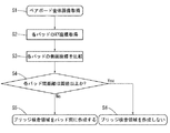
図1は本発明の部品実装基板検査装置の概略的な機能ブロック図、図2は本発明の半田ブリッジ検査ポイントの設定の手順を示すフローチャート、そして図3は半田ブリッジ検査ポイントの設定を説明するためのパッド間距離の狭い一部電極パッド列の平面図である。 FIG. 1 is a schematic functional block diagram of a component mounting board inspection apparatus according to the present invention, FIG. 2 is a flowchart showing a procedure for setting a solder bridge inspection point according to the present invention, and FIG. 3 illustrates setting of a solder bridge inspection point. It is a top view of the partial electrode pad row | line | column for which the distance between pads for this is narrow.
先ず、図1を用いて、本発明の部品実装基板検査装置11の構成を説明する。 First, the structure of the component mounting board inspection apparatus 11 of the present invention will be described with reference to FIG.
図1において、符号1はこの部品実装基板検査装置を指す。この部品実装基板検査装置11は、大きく分けて画像取込手段(A)と画像処理手段(B)とからなる。
In FIG. 1,
検査されるクリーム半田Sが印刷されていない部品実装基板(いわゆるベアボード)Bbは載置手段12に載置されている。 A component mounting board (so-called bare board) Bb on which the cream solder S to be inspected is not printed is placed on the placing means 12.
画像取込手段(A)は、部品実装基板Bbの底面に対する法線に沿って部品実装基板Bbに所定の照射光を照射する第1の照明手段13A、法線とは所定の角度をなす方向に沿って、かつ部品実装基板Bbの周囲から部品実装基板Bbに所定の照射光を照射する第2の照明手段13B、第2の照明手段13Bの法線に対する前記所定の角度より更に大きい角度なす照射光で部品実装基板Bbを照射する第3の照明手段13C、部品実装基板Bbの底面に対する法線方向に配置されており、第1の照明手段13A、第2の照明手段13B、第3の照明手段13C・・・の少なくとも一つの照明手段から出射された照射光による部品実装基板Bbの表面からの反射光を画像として取り込むカメラ15とから構成されている。
The image capturing means (A) is a first illuminating means 13A for irradiating the component mounting board Bb with a predetermined irradiation light along a normal to the bottom surface of the component mounting board Bb, and a direction that forms a predetermined angle with the normal. The second illumination means 13B for irradiating the component mounting board Bb with predetermined irradiation light from the periphery of the component mounting board Bb, and an angle larger than the predetermined angle with respect to the normal line of the second lighting means 13B. The third illuminating means 13C for irradiating the component mounting board Bb with the irradiation light is disposed in the normal direction to the bottom surface of the component mounting board Bb. The first illuminating means 13A, the second illuminating means 13B, the third illuminating means It comprises a
カメラ15から出力されたアナログ信号はデジタル信号に変換するアナログ/デジタル(AD)変換手段16でAD変換され、そのデジタル信号は画像処理手段(B)に入力される。その画像処理手段(B)は、2値化手段17、2値化画像記憶手段18、位置座標取得手段19、近傍距離測定手段20、近傍距離をしきい値と比較する手段21とから構成されている。
The analog signal output from the
部品実装基板Bbの特性値として取り出すものは、部品実装基板Bb上の各電極パッドの面積、位置(x、y座標)である。従って、前記の各特性値を、少なくとも所定のレベル以上の強度を有する反射光の存在する部位が形成する画像上での領域の面積及び位置に対応させて検出する。 What is extracted as the characteristic value of the component mounting board Bb is the area and position (x, y coordinates) of each electrode pad on the component mounting board Bb. Therefore, each of the characteristic values is detected in correspondence with the area and position of the region on the image formed by the portion where the reflected light having the intensity of at least a predetermined level is present.
第1の照明手段13Aは、部品実装基板Bbの法線方向の上方から、部品実装基板Bbのほぼ中央部を中心に部品実装基板Bbに対して均等に照明が照射されるように構成されたものであれば、如何なるものでもよい。 The first illumination means 13A is configured so that illumination is evenly applied to the component mounting board Bb from above the normal direction of the component mounting board Bb, with the central portion of the component mounting board Bb being the center. Any thing can be used.
第2の照明手段13Bは、部品実装基板Bbの斜め上方から光を照射させ、それによる反射光が、カメラ15に入力するように構成されたものであればよい。
The second illuminating means 13 </ b> B only needs to be configured to irradiate light from obliquely above the component mounting board Bb and input reflected light to the
更に、第3の照明手段13Cは、第2の照明手段2Cの部品実装基板Bbの法線方向から前記斜め上方の角度より更に大きい角度を形成する方向から部品実装基板Bbに対して検査光を照射するようにすること望ましく、その角度は特に限定されないが、好ましくはできるだけ部品実装基板Bbに対して水平に近い斜め上方から照射するように構成されるものである。 Further, the third illuminating means 13C emits inspection light to the component mounting board Bb from a direction that forms an angle larger than the obliquely upward angle from the normal direction of the component mounting board Bb of the second illuminating means 2C. It is desirable to irradiate, and the angle is not particularly limited, but it is preferably configured to irradiate the component mounting board Bb as far as possible from an obliquely upward direction.
第1の照明手段13A、第2の照明手段13B、第3の照明手段13Cは、それぞれを独立的に、或いは同時的に駆動させることが可能であり、また、検査すべき部品実装基板Bbの種類によって、その何れかを選択して使用することができる。このような照明手段13A、3B、3Cの駆動を制御するための制御手段14が設けられている。 The first illuminating means 13A, the second illuminating means 13B, and the third illuminating means 13C can be driven independently or simultaneously, and the component mounting board Bb to be inspected can be driven. Either of them can be selected and used depending on the type. Control means 14 is provided for controlling the driving of such illumination means 13A, 3B, 3C.
一方、カメラ15は、部品実装基板Bbのほぼ上方で、部品実装基板Bbのほぼ中央部の法線上にその中心光軸が配置されるように設けられることが望ましい。また、カメラ15は、部品実装基板Bbから反射された反射光を画像情報として取り込むことができるカメラであることが望ましく、例えば、CCDカメラなどが使用できる。
On the other hand, it is desirable that the
次に、部品実装基板検査装置11においては、照明手段とカメラ15とが一体となって制御手段14の下に移動し、例えば、4000ポイントというような検査しなければならない多数のポイントを所定のプログラムに従って順次スキャンし、カメラ15が出力するアナログ情報をデジタル情報に変換するAD変換手段16を介して所定の画像処理を実行する画像処理手段(B)に入力する。画像処理手段(B)は、AD変換手段16から出力されるデジタル信号から、部品実装基板Bbの表面から反射された反射光の内から予め定められた基準値を超える反射光強度を示す反射光を選択、抽出し、予め定められた基準値を超える反射光強度を示す反射光が発生する部品実装基板Bbの部位を示す画像を作成するものである。
Next, in the component mounting board inspection apparatus 11, the illumination unit and the
具体的には、画像処理手段(B)は、入力されたデジタル情報に予め定められたしきい値を適用して2値化する2値化手段17、その2値化手段17により得られた2値化データに基づいた画像を作成し、記憶する画像記憶手段18、その画像記憶手段18に記憶されている2値化画像データから各電極パッドの位置(x、y座標)データを取得する位置座標取得手段19、各電極パッドの位置(x、y座標)データから隣接する電極パッドのパッド間距離(近傍距離)を測定する近傍距離測定手段20、測定された各パッド間距離とオペレータ等により人為的に初期設定しておいたしきい値と比較する手段21とから構成されているものである。
Specifically, the image processing means (B) is obtained by the binarizing means 17 for binarizing the input digital information by applying a predetermined threshold value, and the binarizing means 17 An
初期設定したこのしきい値は、部品実装基板Bbに形成されている各電極パッドのパッド間距離Dの半田ブリッジが生じやすいと判断される距離である。例えば、前記図5に示したBGA型ICやQFP型ICを実装する電極パッド1A、1B、1C・・・のパッド間距離Dが予め極めて狭いことが判っており、そのパッド間距離は前記のように500μm程度と狭いことからその500μmをしきい値として初期設定しておく。
This initially set threshold value is a distance at which it is determined that a solder bridge having an inter-pad distance D between the electrode pads formed on the component mounting board Bb is likely to occur. For example, it is known that the inter-pad distance D of the
次に、図2及び図3をも用いて本発明の部品実装基板検査装置11の動作を説明する。 Next, the operation of the component mounting board inspection apparatus 11 of the present invention will be described with reference to FIGS.
先ず、電極パッドなどにクリーム半田が印刷されていない部品実装基板(ベアボード)Bbを載置手段12に載置、固定し、何れかの照明手段、例えば、第2の照明手段13Bからの照射光を斜め上方から部品実装基板Bbの各電極パッドに順次照射し、それらの画像を2値化手段17で2値化し、それら2値化画像を2値化画像記憶手段18に書き込む(ステップS1)。 First, a component mounting board (bare board) Bb in which cream solder is not printed on an electrode pad or the like is placed and fixed on the placing means 12, and light emitted from any one of the illumination means, for example, the second illumination means 13B. Are sequentially irradiated onto the electrode pads of the component mounting board Bb from above, the images are binarized by the binarizing means 17, and the binarized images are written in the binarized image storage means 18 (step S1). .
次に、位置座標取得手段19で各電極パッドのx軸方向及びy軸方向の座標を取得し(ステップS2)、それら各電極パッドの側面座標、即ち、隣接する電極パッドのパッド間距離を近傍距離測定手段20で測定する。 Next, the position coordinate acquisition means 19 acquires the coordinates in the x-axis direction and the y-axis direction of each electrode pad (step S2), and the side coordinate of each electrode pad, that is, the inter-pad distance between adjacent electrode pads is close. The distance is measured by the distance measuring means 20.
次に、近傍距離をしきい値と比較する手段21において、近傍距離測定手段20で測定したパッド間距離(近傍距離)を予め初期設定したおいたしきい値、例えば、500μmとを比較する(ステップS4)。そして前記パッド間距離がしきい値以下の場合は、半田ブリッジ検査を実行する半田ブリッジ検査ポイントPb(ハッチング部分)を作成し(ステップS5)、前記パッド間距離がしきい値以上の場合は、半田ブリッジ検査を行う半田ブリッジ検査ポイントPbは作成せず、検査ポイントPaのみを作成する(ステップS6)。
Next, the
この半田ブリッジ検査ポイントPbを作成する場合、図3に示したように、各電極パッド1A、1B、1C・・・の右方向と各電極パッド1D、1E、1F・・・の上方向にのみ半田ブリッジ検査ポイントPbを作成する。そして各検査ポイントで「半田ブリッジ不良右側」、「半田ブリッジ不良上側」と発声させ、オペレータに通知するように設定しておく。なお、パッド間距離Dはしきい値未満である。
When creating this solder bridge inspection point Pb, as shown in FIG. 3, only the right direction of each
このように半田ブリッジ検査ポイントを部品実装基板検査装置11に自動で設定することにより、各電極パッド上にクリーム半田Sを印刷した部品実装基板Bを載置台12し、前記のように画像取込手段(A)を順次移動させ、何れかの照明手段で照明しながらカメラ15で画像を取り込み、パッド間距離Dのしきい値より狭い部分を検出すると、半田ブリッジ検査ポイントPbがパッド間に自動的に展開され、図7に示したように、半田ブリッジSbが発生しているか否かを検出することができる。半田ブリッジSbが検出された場合は、そのクリーム半田部分を、例えば、赤色に塗りつぶし、オペレータが画像表示装置上で認識しやすいようにするとよい。
In this way, by automatically setting the solder bridge inspection point in the component mounting board inspection apparatus 11, the component mounting board B having the cream solder S printed on each electrode pad is placed on the mounting table 12, and the image is captured as described above. When the means (A) is sequentially moved and an image is captured by the
従って、本発明の部品実装基板検査装置11によれば、半田ブリッジ検査ポイントを自動で設定することができ、このことにより、オペレータは手動設定する手間と時間を掛けずに最適な検査結果を出力することができる。 Therefore, according to the component mounting board inspection apparatus 11 of the present invention, it is possible to automatically set the solder bridge inspection point, which allows the operator to output an optimal inspection result without taking time and effort for manual setting. can do.
11 本発明の一実施例の部品実装基板検査装置
13A 第1照明手段
13B 第2照明手段
13C 第3照明手段
14 制御手段
15 カメラ
17 2値化手段
18 2値化画像記憶手段
19 位置座標取得手段
20 近傍距離測定手段
21 近傍距離をしきい値と比較する手段
B 部品実装基板
Bb 部品実装基板(ベアボード)
DESCRIPTION OF SYMBOLS 11 Component mounting board inspection apparatus of one Example of this invention 13A 1st illumination means 13B 2nd illumination means 13C 3rd illumination means 14 Control means 15
Claims (1)
照明された前記部品実装基板を撮影し、画像データを出力するカメラ手段と、
前記画像データを2値化する2値化手段と、
前記2値化された画像を記憶する2値化画像記憶手段と、
前記記憶された2値化画像から前記各電極パッドの位置座標を取得する位置座標取得手段と、
前記各電極パッドの位置座標から隣接する電極パッドのパッド間距離を測定する近傍距離測定手段と、
前記各パッド間距離を人為的に設定されたしきい値と比較する比較手段と、
前記パッド間距離が前記しきい値より狭い場合に半田ブリッジ検査ポイントを設定する半田ブリッジ検査ポイント設定手段と
を備えていることを特徴とする部品実装基板検査装置。 Illuminating means for illuminating a component mounting board on which a plurality of electrode pads are formed at predetermined intervals;
Camera means for photographing the illuminated component mounting board and outputting image data;
Binarization means for binarizing the image data;
Binarized image storage means for storing the binarized image;
Position coordinate acquisition means for acquiring position coordinates of each electrode pad from the stored binary image;
Proximity distance measuring means for measuring a distance between adjacent electrode pads from the position coordinates of each of the electrode pads;
A comparing means for comparing the distance between the pads with an artificially set threshold;
A component mounting board inspection apparatus comprising: a solder bridge inspection point setting means for setting a solder bridge inspection point when the distance between the pads is smaller than the threshold value.
Priority Applications (5)
| Application Number | Priority Date | Filing Date | Title |
|---|---|---|---|
| JP2004032567A JP4051568B2 (en) | 2004-02-09 | 2004-02-09 | Component mounting board inspection equipment |
| KR1020050005373A KR101129349B1 (en) | 2004-02-09 | 2005-01-20 | Parts mount board inspection apparatus |
| US11/039,902 US7664311B2 (en) | 2004-02-09 | 2005-01-24 | Component mounting board inspecting apparatus |
| TW094102026A TW200538007A (en) | 2004-02-09 | 2005-01-24 | Inspection device of component mounting substrate |
| CNB2005100052115A CN100510723C (en) | 2004-02-09 | 2005-02-01 | Component mounting board inspecting apparatus |
Applications Claiming Priority (1)
| Application Number | Priority Date | Filing Date | Title |
|---|---|---|---|
| JP2004032567A JP4051568B2 (en) | 2004-02-09 | 2004-02-09 | Component mounting board inspection equipment |
Publications (2)
| Publication Number | Publication Date |
|---|---|
| JP2005223281A JP2005223281A (en) | 2005-08-18 |
| JP4051568B2 true JP4051568B2 (en) | 2008-02-27 |
Family
ID=34908318
Family Applications (1)
| Application Number | Title | Priority Date | Filing Date |
|---|---|---|---|
| JP2004032567A Expired - Fee Related JP4051568B2 (en) | 2004-02-09 | 2004-02-09 | Component mounting board inspection equipment |
Country Status (5)
| Country | Link |
|---|---|
| US (1) | US7664311B2 (en) |
| JP (1) | JP4051568B2 (en) |
| KR (1) | KR101129349B1 (en) |
| CN (1) | CN100510723C (en) |
| TW (1) | TW200538007A (en) |
Families Citing this family (11)
| Publication number | Priority date | Publication date | Assignee | Title |
|---|---|---|---|---|
| JP4471904B2 (en) | 2005-08-01 | 2010-06-02 | 豊田鉄工株式会社 | Bumper beam for automobile |
| JP4103921B2 (en) * | 2006-08-11 | 2008-06-18 | オムロン株式会社 | Method of setting inspection reference data for fillet inspection, and substrate visual inspection apparatus using this method |
| KR101133968B1 (en) * | 2009-07-03 | 2012-04-05 | 주식회사 고영테크놀러지 | Method for detecting a bridge connecting failure |
| JP4969664B2 (en) * | 2010-03-03 | 2012-07-04 | シーケーディ株式会社 | Solder printing inspection apparatus and solder printing system |
| JP5338773B2 (en) * | 2010-08-26 | 2013-11-13 | パナソニック株式会社 | Component mounting apparatus, imaging illumination apparatus, and illumination method |
| JP2013115194A (en) * | 2011-11-28 | 2013-06-10 | Nagoya Electric Works Co Ltd | Solder position analysis device, substrate appearance inspection device, solder position analysis method and solder position analysis program |
| WO2014171890A1 (en) * | 2013-04-15 | 2014-10-23 | Heptagon Micro Optics Pte. Ltd. | Accurate positioning and alignment of a component during processes such as reflow soldering |
| JP5911899B2 (en) * | 2014-02-17 | 2016-04-27 | Ckd株式会社 | Board inspection apparatus and component mounting apparatus |
| JP6267366B2 (en) * | 2014-05-05 | 2018-01-24 | アーコニック インコーポレイテッドArconic Inc. | Welding measuring device and method |
| CN107529280A (en) * | 2017-08-31 | 2017-12-29 | 郑州云海信息技术有限公司 | The method and device that a kind of Foot print are established |
| CN111998815A (en) * | 2020-07-29 | 2020-11-27 | 北京浪潮数据技术有限公司 | Method for detecting PAD (PAD application) space between devices on PCB (printed circuit board) and related device |
Family Cites Families (14)
| Publication number | Priority date | Publication date | Assignee | Title |
|---|---|---|---|---|
| JPS61288106A (en) | 1985-06-17 | 1986-12-18 | Fujitsu Ltd | Inspecting method for pattern cut width |
| US5621811A (en) * | 1987-10-30 | 1997-04-15 | Hewlett-Packard Co. | Learning method and apparatus for detecting and controlling solder defects |
| JP3092809B2 (en) * | 1989-12-21 | 2000-09-25 | 株式会社日立製作所 | Inspection method and inspection apparatus having automatic creation function of inspection program data |
| JP3105353B2 (en) | 1992-06-30 | 2000-10-30 | 松下電器産業株式会社 | Cream solder printing inspection equipment |
| US5991435A (en) * | 1992-06-30 | 1999-11-23 | Matsushita Electric Industrial Co., Ltd. | Inspecting apparatus of mounting state of component or printing state of cream solder in mounting line of electronic component |
| CA2113752C (en) * | 1994-01-19 | 1999-03-02 | Stephen Michael Rooks | Inspection system for cross-sectional imaging |
| JPH10160426A (en) | 1996-12-03 | 1998-06-19 | Nec Corp | Method and equipment for inspecting object to be inspected |
| US6317513B2 (en) * | 1996-12-19 | 2001-11-13 | Cognex Corporation | Method and apparatus for inspecting solder paste using geometric constraints |
| US6118893A (en) * | 1997-07-16 | 2000-09-12 | Cognex Corporation | Analysis of an image of a pattern of discrete objects |
| US6130959A (en) * | 1997-07-16 | 2000-10-10 | Cognex Corporation | Analyzing an image of an arrangement of discrete objects |
| KR100281881B1 (en) * | 1998-07-01 | 2001-02-15 | 윤종용 | cream solder inspection apparatus and the method thereof |
| JP4154771B2 (en) * | 1998-11-10 | 2008-09-24 | ソニー株式会社 | Nonvolatile semiconductor memory device and data writing method thereof |
| DE60312182T2 (en) * | 2002-07-25 | 2007-06-21 | Matsushita Electric Industrial Co., Ltd., Kadoma | DEVICE AND METHOD FOR EXAMINING SUBSTRATE IMPRINTED CREAM LOT |
| US7233871B2 (en) * | 2003-03-10 | 2007-06-19 | Landrex Technologies Co., Ltd. | Inspection window guard banding |
-
2004
- 2004-02-09 JP JP2004032567A patent/JP4051568B2/en not_active Expired - Fee Related
-
2005
- 2005-01-20 KR KR1020050005373A patent/KR101129349B1/en not_active IP Right Cessation
- 2005-01-24 TW TW094102026A patent/TW200538007A/en not_active IP Right Cessation
- 2005-01-24 US US11/039,902 patent/US7664311B2/en not_active Expired - Fee Related
- 2005-02-01 CN CNB2005100052115A patent/CN100510723C/en not_active Expired - Fee Related
Also Published As
| Publication number | Publication date |
|---|---|
| KR20050080442A (en) | 2005-08-12 |
| KR101129349B1 (en) | 2012-03-27 |
| TW200538007A (en) | 2005-11-16 |
| JP2005223281A (en) | 2005-08-18 |
| CN100510723C (en) | 2009-07-08 |
| US7664311B2 (en) | 2010-02-16 |
| US20050196996A1 (en) | 2005-09-08 |
| CN1654947A (en) | 2005-08-17 |
| TWI294759B (en) | 2008-03-11 |
Similar Documents
| Publication | Publication Date | Title |
|---|---|---|
| KR101129349B1 (en) | Parts mount board inspection apparatus | |
| JP5256251B2 (en) | Inspection method of measurement object | |
| JPH0572961B2 (en) | ||
| JP4684033B2 (en) | Board inspection equipment | |
| JP2004226319A (en) | Visual inspection apparatus and image acquisition method | |
| JP5124705B1 (en) | Solder height detection method and solder height detection device | |
| JP2007139676A (en) | Device and method for inspecting substrate | |
| JP4734650B2 (en) | Defect detection method and apparatus for cream solder printing | |
| JP4131804B2 (en) | Mounting component inspection method | |
| JP3597484B2 (en) | Solder printing inspection equipment | |
| KR101056995B1 (en) | 3D shape inspection method | |
| KR101133972B1 (en) | Method of inspecting terminal | |
| JPH05288527A (en) | Appearance inspecting method for mounted board and its device | |
| JP4862149B2 (en) | Inspection method and apparatus for cream solder printing | |
| JPH05280946A (en) | Observing apparatus of board | |
| KR101133641B1 (en) | Method of inspecting three-dimensional shape | |
| JP2005223006A (en) | Inspection method of cream solder print | |
| JPH1090191A (en) | Soldering testing equipment | |
| JP3038107B2 (en) | Soldering inspection method | |
| JP2010091529A (en) | Method and apparatus for inspecting printed circuit board | |
| JP4180127B2 (en) | Cream solder printing inspection apparatus and cream solder printing inspection method | |
| JP2629798B2 (en) | Board inspection equipment | |
| JP2003224354A (en) | Soldering appearance inspection method and apparatus thereof | |
| JP2765338B2 (en) | Chip component mounting inspection equipment | |
| JPH04279808A (en) | Paste solder printing condition inspection device |
Legal Events
| Date | Code | Title | Description |
|---|---|---|---|
| A977 | Report on retrieval |
Free format text: JAPANESE INTERMEDIATE CODE: A971007 Effective date: 20070730 |
|
| A131 | Notification of reasons for refusal |
Free format text: JAPANESE INTERMEDIATE CODE: A131 Effective date: 20070808 |
|
| A521 | Written amendment |
Free format text: JAPANESE INTERMEDIATE CODE: A523 Effective date: 20071009 |
|
| TRDD | Decision of grant or rejection written | ||
| A01 | Written decision to grant a patent or to grant a registration (utility model) |
Free format text: JAPANESE INTERMEDIATE CODE: A01 Effective date: 20071107 |
|
| A61 | First payment of annual fees (during grant procedure) |
Free format text: JAPANESE INTERMEDIATE CODE: A61 Effective date: 20071120 |
|
| FPAY | Renewal fee payment (event date is renewal date of database) |
Free format text: PAYMENT UNTIL: 20101214 Year of fee payment: 3 |
|
| FPAY | Renewal fee payment (event date is renewal date of database) |
Free format text: PAYMENT UNTIL: 20101214 Year of fee payment: 3 |
|
| FPAY | Renewal fee payment (event date is renewal date of database) |
Free format text: PAYMENT UNTIL: 20111214 Year of fee payment: 4 |
|
| FPAY | Renewal fee payment (event date is renewal date of database) |
Free format text: PAYMENT UNTIL: 20121214 Year of fee payment: 5 |
|
| FPAY | Renewal fee payment (event date is renewal date of database) |
Free format text: PAYMENT UNTIL: 20131214 Year of fee payment: 6 |
|
| R250 | Receipt of annual fees |
Free format text: JAPANESE INTERMEDIATE CODE: R250 |
|
| R250 | Receipt of annual fees |
Free format text: JAPANESE INTERMEDIATE CODE: R250 |
|
| LAPS | Cancellation because of no payment of annual fees |