JP4043121B2 - Electronic component mounting apparatus and method - Google Patents
Electronic component mounting apparatus and method Download PDFInfo
- Publication number
- JP4043121B2 JP4043121B2 JP35579198A JP35579198A JP4043121B2 JP 4043121 B2 JP4043121 B2 JP 4043121B2 JP 35579198 A JP35579198 A JP 35579198A JP 35579198 A JP35579198 A JP 35579198A JP 4043121 B2 JP4043121 B2 JP 4043121B2
- Authority
- JP
- Japan
- Prior art keywords
- electronic component
- interference
- electronic components
- electronic
- rotation
- Prior art date
- Legal status (The legal status is an assumption and is not a legal conclusion. Google has not performed a legal analysis and makes no representation as to the accuracy of the status listed.)
- Expired - Fee Related
Links
Images


Description
【0001】
【発明の属する技術分野】
本発明は、例えば電子部品を電子回路基板(以下単に「回路基板」と記す)上に装着するような部品装着ヘッドを備えた電子部品装着装置、及び該電子部品装着装置にて実行される電子部品装着方法に関する。
【0002】
【従来の技術】
近年、電子部品を回路基板上に装着する電子部品実装装置は、上記回路基板に上記電子部品を速く正確に装着し、実装品質を向上させることが要求されている。
以下、図8及び図9を参照して従来の電子部品実装装置及び該電子部品実装装置にて実行される電子部品実装方法について説明する。
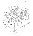
従来の電子部品実装装置1は、大別して、当該実装工程の前工程から回路基板20を搬入し、次工程へ搬出する基板搬送装置12と、複数の部品供給ユニットを有する部品供給装置13と、ヘッド部15と、基板認識カメラ16と、XYロボット17と、部品撮像装置18と、部品廃棄部19とを備える。
上記ヘッド部15は、図9に示すように、吸着動作により電子部品51〜54を保持する複数の吸着ノズルであって実装する電子部品に応じて着脱交換可能な吸着ノズル41〜44を備え、回路基板20へ電子部品51〜54を装着するために上記吸着ノズル41〜44が移動する方向、言い換えるとZ軸方向へ上記吸着ノズル41〜44を移動させる昇降機構45〜48、さらに上記吸着ノズル41〜44をその軸回り方向へ回転させる回転機構を有する。このようなヘッド部15は、上記XYロボット17に取り付けられX、Y軸方向へ移動可能である。
上記基板認識カメラ16は、上記部品供給装置13から上記吸着ノズル41〜44にて保持された電子部品の保持姿勢の良否を判定するために上記電子部品の保持姿勢を撮像する。その結果、保持姿勢が不良と判断されたときには、不良と判断された電子部品を保持している吸着ノズルを上記XYロボット17にて上記部品廃棄部19まで移動させて不良と判断された電子部品を廃棄する。上記部品廃棄部19はベルトコンベヤ機構を備え、上記ヘッド部15にて上記ベルトコンベヤ機構のベルト19a上に載置された上記不良と判断された電子部品を不図示の廃棄箱へ搬送する。
【0003】
このような従来の電子部品実装装置1は、以下のように動作する。回路基板20は、基板搬送装置12により装着位置に搬入される。XYロボット17は、基板認識カメラ16を回路基板上に移動し、実装すべき位置を調べる。次に、XYロボット17によりヘッド部15を部品供給部13に移動させ、それぞれの吸着ノズル41〜44にて電子部品51〜54をそれぞれ保持させる。吸着ノズル41〜44に保持された電子部品51〜54は、部品撮像装置18にて保持姿勢が撮像され、不図示の制御装置にて電子部品の保持姿勢が計測され、該保持姿勢の良否が判定される。
次に電子部品51〜54の保持姿勢計測結果が正常であれば、上記撮像動作にて得られた画像情報をもとに電子部品51〜54のX、Y方向への位置補正を行い装着方向を回路基板20上の実装すべき位置に一致させる。その後、XYロボット17により電子部品51〜54が上記実装すべき位置に対応するようにヘッド部15を移動させ、吸着ノズル41〜44の各々に保持されている電子部品51〜54を装着高さまで下降させ回路基板20上に装着する。
一方、電子部品51〜54の保持姿勢計測結果に異常があれば、設置された部品廃棄部13へXYロボット17によりヘッド部15を移動させ、吸着ノズル41〜44に保持されている電子部品51〜54の内、保持姿勢結果異常の電子部品のみを廃棄する。
【0004】
【発明が解決しようとする課題】
上述のように、電子部品51〜54の装着方向を回路基板20上の実装すべき位置に一致させるため、電子部品51〜54を保持した吸着ノズル41〜44を回転軸の軸回り方向に回転させる。このとき、図9に示すように、互いに隣接している吸着ノズル、例えば吸着ノズル41、42が吸着保持している電子部品51、52について、上記吸着ノズル41、42の回転軸を中心としたそれぞれの電子部品51、52の回転半径r1,r2の合計が吸着ノズル41、42間の配置ピッチp1より大きい場合には、隣接する吸着ノズル41、42が吸着保持している電子部品51、52を同時に回転させたときには、電子部品51、52同士が干渉する可能性がある。
よって上記干渉が生じたときには、吸着保持している電子部品の落下、及び装着精度の劣化を招き、結果として生産効率が低下するという問題点がある。
本発明は、このような問題点を解決するためになされたもので、複数の部品保持部材が隣接して配置されている場合において生産効率の低下を生じない電子部品装着装置、及び電子部品装着方法を提供することを目的とする。
【0005】
【課題を解決するための手段】
本発明の第1態様の電子部品装着装置は、互いに隣接して配置され電子部品を保持する少なくとも2つの保持部材を有し、それぞれの上記電子部品を回路基板へ装着するため上記電子部品を保持したそれぞれの上記保持部材が当該保持部材における回転軸の軸回り方向に回転可能である部品装着ヘッドを備えた電子部品装着装置であって、
上記電子部品を保持した上記保持部材について上記回転を行うとき、一方の保持部材に保持されている電子部品が他方の保持部材に保持されている電子部品に干渉するか否かを判断し、干渉するときには干渉回避動作を行なわせた後、上記部品装着ヘッドに対して上記回転を行わせる制御装置を備え、
上記干渉回避動作は、干渉する電子部品間で該干渉を回避できる最小限の回転角度である干渉回避角度にて上記保持部材の内の一方の保持部材を上記軸回り方向へ回転した後、上記他方の保持部材の回転を開始する動作である、
ことを特徴とする。
【0008】
又、本発明の第2態様の電子部品装着方法は、互いに隣接して配置される少なくとも2つの保持部材に保持されているそれぞれの電子部品を上記保持部材における回転軸の軸回り方向に回転することで上記電子部品と回路基板への装着位置とを一致させて上記電子部品を上記回路基板へ装着する電子部品装着方法であって、
上記電子部品について上記回転を行うとき、隣接する上記電子部品間で干渉が生じるか否かを判断し、干渉するときには、干渉する電子部品間で該干渉を回避できる最小限の回転角度である干渉回避角度にて一方の電子部品を上記軸回り方向へ回転した後、他方の電子部品の回転を開始する干渉回避動作を行なった後、上記回転を行なうことを特徴とする。
【0009】
【発明の実施の形態】
本発明の実施形態である、電子部品装着装置及び該電子部品装着装置にて実行される電子部品部品装着方法について、図を参照しながら以下に説明する。尚、各図において同じ構成部分については同じ符号を付している。
又、上記「課題を解決するための手段」に記載する、「保持部材」の機能を果たす一例として、本実施形態では吸着ノズルを例に採るがこれに限定されるものではなく、例えば機械的に電子部品を保持するような部材であっても良い。
【0010】
図1に示す本実施形態における電子部品装着装置101は、基本的に上述した従来の電子部品実装装置1における構成と同じ構成を有するが、電子部品装着装置101では詳細後述する、隣接する電子部品同士の干渉回避動作を実行させる制御装置180を備えた点が特徴となる。即ち、電子部品装着装置101は、大別して、当該電子部品実装工程の前工程から回路基板20を搬入し、次工程へ搬出する基板搬送装置112と、複数の部品供給ユニットを有する部品供給装置113と、部品装着ヘッド115と、基板認識カメラ116と、XYロボット117と、部品撮像装置118と、部品廃棄部119とを備える。ここで、上記基板搬送装置112は上述した従来の基板搬送装置12に相当し、上記部品供給装置113は上述した従来の部品供給装置13に相当し、上記部品装着ヘッド115は上述した従来のヘッド部15に相当し、上記基板認識カメラ116は上述した従来の基板認識カメラ16に相当し、上記XYロボット117は上述した従来のXYロボット17に相当し、上記部品撮像装置118は上述した従来の部品撮像装置18に相当し、上記部品廃棄部119は上述した従来の部品廃棄部19に相当する。よって、これらの上記基板搬送装置112、上記部品供給装置113、上記部品装着ヘッド115、上記基板認識カメラ116、上記XYロボット117、上記部品撮像装置118、及び上記部品廃棄部119について、以下に示すように補足説明を加えるものを除き、ここでの詳しい説明は省略する。又、これらの構成部分はそれぞれ上記制御装置180に接続され動作制御がなされる。
【0011】
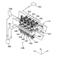
部品装着ヘッドは、X軸方向に沿って列状に互いに隣接して少なくとも2つの吸着ノズルを配列しており、本実施形態における部品装着ヘッド115では図3及び図4に示すように4つの吸着ノズル141〜144を配列している。これらの吸着ノズル141〜144は、上述した従来の吸着ノズル41〜44と同様に、実装する電子部品に応じて部品装着ヘッド115に対して着脱交換可能であり、駆動部145〜148を有する昇降機構にてそれぞれ上記Z軸方向に沿って昇降可能である。これらの駆動部145〜148のそれぞれは、上記制御装置180に接続されており、制御装置180にて昇降動作及び昇降移動量が制御される。又、上記吸着ノズル141〜144は、上記制御装置180にて動作制御される吸引装置151により吸着動作にて電子部品を保持する。尚、電子部品の保持方法は、上記吸引動作に限定されるものではなく、例えば機械的な保持方法等を採用することができる。
上記吸着ノズル141〜144のそれぞれは、モータ等にてなる駆動部152〜155を有する回転機構にて、該吸着ノズル141〜144の回転軸156を中心にその軸回り方向に回転可能である。尚、回転方向及び回転角度は、上記制御装置180による上記駆動部152〜155の動作制御にて制御される。
【0012】
図3にX軸方向に沿って部品装着ヘッド115を移動させるXロボットに示されるように、XYロボット117は、いわゆるボールねじ構造にて構成され、回転シャフト157と、該回転シャフト157をその軸回り方向へ回転させる例えばモータ等の駆動部158とを備え、制御装置180による駆動部158の動作制御にて部品装着ヘッド115のX軸、Y軸方向への移動量が調整される。
【0013】
各電子部品について、制御装置180には、装着順、回路基板20における装着位置等の実装動作に関する情報、及び寸法情報が少なくとも供給され、制御装置180は、上記実装動作に関する情報に基づき電子部品装着装置101における上述の各構成部分の動作制御を行う。制御装置180の制御動作のうち、ここでは本実施形態において特徴的な動作制御である、上記干渉回避動作の制御について説明する。
従来の電子部品実装装置1の場合と同様に、部品装着ヘッド115の吸着ノズル141〜144にて電子部品51〜54がそれぞれ吸着された後、それぞれの電子部品51〜54は部品撮像装置118にて撮像され保持姿勢がチェックされる。そして各電子部品51〜54は、回路基板20の上記装着位置における回路基板20の電極と当該電子部品のリードとが一致するように、吸着ノズル141〜144の回転軸156の軸回り方向へ吸着ノズル141〜144を回転することで回転される。
【0014】
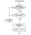
このような電子部品51〜54の回転を行うとき、制御装置180は、図2に示すような動作制御を行う。尚、以下の説明において、隣接する電子部品として電子部品51と電子部品52とを例に採る。
ステップ(図では「S」にて示す)1では、隣接する電子部品51と電子部品52について、それぞれの回転半径寸法の合計値がこれらの電子部品51、52を保持している隣接する吸着ノズル141、142の配置間隔寸法p11を超えるか否かが制御装置180にて判断される。つまり、制御装置180は、供給されている、上記実装動作に関する情報に基づき実装動作を実行しているので、各吸着ノズル141〜144に保持されている電子部品51〜54を認識しており、これら電子部品51〜54の上記寸法情報に基づき上記電子部品51及び電子部品52の回転半径寸法を求める。ここで上記回転半径寸法とは、例えば電子部品51を例に採ると、上記回転軸156を中心として描いた円内に電子部品51のすべてのリードが収まるような円の内、最小の円における半径寸法であり、図4に示す半径r11が相当する。同様に、電子部品52についても上記最小半径寸法の半径r12を求める。そして制御装置180は、上記半径r11と半径12とを加算した値が、吸着ノズル141、142の配置間隔寸法p11を超えるか否かを判断する。
尚、上述の説明では、上記回転軸156と電子部品52の中心とが一致していることを前提にしている。これは本来、吸着ノズル141、142は電子部品52の中心を吸着するように設定されているからである。
【0015】
上記ステップ1にて上記半径r11と半径12とを加算した値が、上記配置間隔寸法p11を超えないときには、電子部品51と電子部品52とは干渉しないので、ステップ3にて、両方の電子部品51、52を同時に回転することができる。もちろん、後述のように時間差を設けて回転動作を行っても良い。
【0016】
一方、上記ステップ1にて上記半径r11と半径12とを加算した値が、上記配置間隔寸法p11を超えるときには、電子部品51と電子部品52とを同時に回転させたときには両者は干渉することになる。そこで、ステップ2では、制御装置180は、隣接する電子部品51、52が吸着ノズル141、142の昇降方向、つまり上記Z軸方向に沿って同一レベルに有るか否かを判断する。即ち、隣接する電子部品51,52は、上記回転動作によって初めて干渉し合うのであり、吸着された時点では干渉していない。よってステップ1において、上記加算値が上記配置間隔寸法p11を超えると判断されたとしても、上記回転により両者が干渉しない程度に上記Z軸方向に沿って異レベルに配置されていれば、両者を同時に回転させることは可能である。そこでステップ2では、回転動作において、隣接する電子部品51,52間で干渉が生じるか否かが判断される。
そして、両者で干渉が生じないときには、ステップ3にて両者を同時に回転させることも可能である。
【0017】
一方、ステップ2においても、隣接する電子部品51,52間で干渉が生じると判断されたときには、つまり電子部品51,52が上記Z軸方向に沿って同一レベルに配置されているときには、制御装置180は、ステップ4にて、電子部品51,52の内のいずれか一方について干渉回避動作を行った後、ステップ5にて電子部品51、52について回転を開始する。
【0018】
上記ステップ4における上記干渉回避動作について図5を参照して詳しく説明する。
上述のようにステップ4に移行したことは、隣接する電子部品51,52が上記Z軸方向に沿って同一レベルに配置されている場合であり、このような状態で電子部品51,52を回転したときに両者の干渉を避けるため、本実施形態では回転動作開始時刻をずらす方法を採っている。尚、説明を簡略化するため、吸着ノズル141〜144に吸着されているすべての電子部品51〜54について、角度θ1から角度θ2まで回転を要するものとし、又、電子部品51〜54は、吸着時点において角度θ1にてそれぞれ吸着ノズル141〜144に吸着されているものとする。又、上述のように制御装置180は各吸着ノズル141〜144に保持されている電子部品51〜54の回転半径を認識していることから、隣接する電子部品間で上記回転を行うときに干渉を回避できる干渉回避角度θ3を予め求めている。
【0019】
このような条件下で、電子部品51,52の内のいずれか一方、例えば電子部品51が電子部品52との干渉を避けるため、電子部品51つまり吸着ノズル141について、角度θ1より回転を開始し一定の回転速度にて回転を行う。そして吸着ノズル141の回転角度が上記干渉回避角度θ3に達した時点で、ステップ5にて、他方の電子部品52を吸着している吸着ノズル142の回転を開始する。尚、このような回転角度の検出は、制御装置180による駆動部152〜155の動作制御にて実行される。
又、残りの電子部品53,54についても同様に動作させる。
このように隣接する電子部品間で回転開始に時間差を設けることで、両者の干渉を避けることができ、よって、実装精度を確保することができ、その結果として生産効率を向上させることができる。
【0020】
上述の説明では、それぞれの吸着ノズル141〜144に吸着されている電子部品51〜54の寸法に基づいた上記回転半径寸法にて干渉の有無を判断しているが、さらに、上記部品撮像装置118にて得られた電子部品51〜54の撮像情報をも加味して上記干渉の有無を判断することもできる。
又、上述の説明では、上記干渉回避角度θ3を超えて電子部品51〜54は回転を要するような場合を例に採ったが、もちろん上記干渉回避角度θ3未満の角度による回転ですむ場合もあり、このような場合には、隣接する電子部品間で干渉は生じないので、両者を同時に回転開始することができる。
【0021】
上記干渉回避動作としては上述の回転動作による回避が最も現実的であるが、その他の方法としては、図6に示すように隣接する電子部品について上記Z軸方向に沿って異レベルに配置するようにしてもよい。即ち、図示するようにリードが電子部品の4辺に配列されているような場合、上記回転により隣接する電子部品において干渉する部分はリードである。よって、隣接する電子部品のリード同士が干渉しないように、隣接する電子部品を上記Z軸方向に沿って異レベルに配置すればよい。
具体的には、リードが4辺に配列されている電子部品の場合、上記Z軸方向に沿って隣接する電子部品の一方を他方に対して異レベルに配置するため、上記一方の電子部品が位置すべき上記Z軸方向の最小限の位置である干渉回避位置は、上記他方の電子部品に対して上記リードの厚み寸法である図7に示す寸法Iを超える位置である。
又、隣接する電子部品において上記回転により干渉する部分が電子部品の本体部分である場合には、上記干渉回避位置は、上記他方の電子部品に対して上記本体の厚み寸法である図7に示す寸法IIを超える位置である。
尚、上記干渉回避位置への電子部品の移動は、制御装置180による駆動部145〜148の動作制御にて実行される。
【0022】
このように隣接する電子部品同士を上記Z軸方向に沿って異レベルに配置した後であれば、隣接する電子部品は同時に上記回転を開始することができる。尚、隣接する電子部品間で、上記回転開始タイミングは同時である必要はなく、少なくとも一方の回転を開始すれば良い。
このように隣接する電子部品同士を上記Z軸方向に沿って異レベルに配置することによっても、上述の回転開始に時間差を設ける場合と同様に、両者の干渉を避けることができ、よって、実装精度を確保することができ、その結果として生産効率を向上させることができる。
【0023】
このように構成される電子部品装着装置101における電子部品装着動作について以下に説明する。
基板搬送装置112により回路基板20が電子部品装着装置101に搬入される。XYロボット117は、基板認識カメラ116を回路基板20上に移動し、電子部品を実装すべき位置の位置データを取った後、部品装着ヘッド115を部品供給部113に移動させ、それぞれの吸着ノズル141〜144にて電子部品51〜54をそれぞれ保持させる。吸着ノズル141〜144に保持された電子部品51〜54は、部品撮像装置118にて保持姿勢が撮像され、制御装置180にて電子部品51〜54の保持姿勢が計測され、保持姿勢の良否が判定される。
【0024】
次に電子部品51〜54の保持姿勢計測結果が正常であれば、上記撮像動作にて得られた画像情報をもとに電子部品51〜54の位置補正がなされた後、電子部品51〜54の装着方向を回路基板20上の実装すべき位置に一致させるように、保持した吸着ノズル141〜144を回転させる。このとき、上述したように、制御装置180は、隣接する電子部品同士での干渉の有無を確認し、干渉が生じるようであれば上記干渉回避動作を実行した後、吸着ノズル141〜144の回転を行う。
上記吸着ノズル141〜144の回転後、XYロボット117により部品装着ヘッド115を上記実装すべき位置に対応するように移動させ、吸着ノズル141〜144の各々に保持されている電子部品51〜54を装着高さまで下降させ回路基板20上に装着する。
【0025】
一方、電子部品51〜54の上記保持姿勢計測結果に異常があれば、部品廃棄部113へXYロボット117により部品装着ヘッド115を移動させ、吸着ノズル141〜144に保持されている電子部品51〜54の内、保持姿勢結果異常の電子部品のみを廃棄する。
【0026】
【発明の効果】
以上詳述したように、本発明の第1態様における電子部品装着装置、及び第2態様の電子部品装着方法によれば、制御装置を備え、電子部品を保持している保持部材について回転軸の軸回り方向へ回転を行うとき、隣接する電子部品同士での干渉の有無を判断し、干渉するときには部品装着ヘッドに対して干渉回避動作を行なわせた後、上記回転を行うようにした。よって、隣接する電子部品間で干渉することがなくなることから、上記干渉による電子部品の落下、及び装着精度の劣化がなくなり、結果として回路基板の生産効率の向上を図ることができる。
【図面の簡単な説明】
【図1】 本発明の実施形態における電子部品装着装置の斜視図である。
【図2】 図1に示す電子部品装着装置における干渉回避動作のフローチャートである。
【図3】 図1に示す電子部品装着装置に備わる部品装着ヘッドの構造を示す斜視図である。
【図4】 図3に示す部品装着ヘッドの吸着ノズルに保持されている電子部品の干渉を説明するための図である。
【図5】 図1に示す電子部品装着装置における干渉回避動作の吸着ノズルの回転のタイミングを示すタイミングチャートである。
【図6】 図1に示す電子部品装着装置の干渉回避動作における吸着ノズルの昇降位置を示す図である。
【図7】 上記吸着ノズルの昇降位置の具体的寸法を説明するための図である。
【図8】 従来の電子部品実装装置を示す斜視図である。
【図9】 図8に示す電子部品実装装置のヘッド部の配置間隔と電子部品の回転半径とを示す図である。
【符号の説明】
101…電子部品装着装置、115…部品装着ヘッド、
141〜144…吸着ノズル、
180…制御装置。[0001]
BACKGROUND OF THE INVENTION
The present invention provides, for example, an electronic component mounting apparatus including a component mounting head for mounting an electronic component on an electronic circuit board (hereinafter simply referred to as “circuit board”), and an electronic device that is executed by the electronic component mounting apparatus. The present invention relates to a component mounting method.
[0002]
[Prior art]
In recent years, an electronic component mounting apparatus for mounting an electronic component on a circuit board is required to mount the electronic component on the circuit board quickly and accurately to improve mounting quality.
Hereinafter, a conventional electronic component mounting apparatus and an electronic component mounting method executed by the electronic component mounting apparatus will be described with reference to FIGS.
The conventional electronic
As shown in FIG. 9, the
The
[0003]
Such a conventional electronic
Next, if the holding posture measurement result of the
On the other hand, if there is an abnormality in the holding posture measurement result of the
[0004]
[Problems to be solved by the invention]
As described above, in order to make the mounting direction of the
Therefore, when the interference occurs, there is a problem that the electronic parts held by suction are dropped and the mounting accuracy is deteriorated, resulting in a decrease in production efficiency.
The present invention has been made to solve such problems, and an electronic component mounting apparatus and an electronic component mounting that do not cause a decrease in production efficiency when a plurality of component holding members are arranged adjacent to each other It aims to provide a method.
[0005]
[Means for Solving the Problems]
An electronic component mounting apparatus according to a first aspect of the present invention includes at least two holding members that are arranged adjacent to each other and hold an electronic component, and hold the electronic component for mounting the electronic component on a circuit board. Each of the holding members is an electronic component mounting apparatus provided with a component mounting head that is rotatable about the axis of rotation of the holding member.
When the holding member holding the electronic component is rotated, it is determined whether the electronic component held by one holding member interferes with the electronic component held by the other holding member. And a control device for causing the component mounting head to perform the rotation after performing an interference avoidance operation .
In the interference avoiding operation, after rotating one holding member of the holding members in the direction around the axis at an interference avoiding angle which is a minimum rotation angle capable of avoiding the interference between the interfering electronic components, The operation of starting the rotation of the other holding member,
It is characterized by that.
[0008]
The electronic component mounting method of the second aspect of the present invention, the rotation of each of the electronic components held by the at least two holding members are arranged adjacent to each other around the axis of the rotary shaft in the holding member An electronic component mounting method for mounting the electronic component on the circuit board by matching the mounting position on the circuit board with the electronic component,
When performing the rotation of the electronic component, it is determined whether interference occurs between the adjacent electronic components. When the interference occurs, the interference is the minimum rotation angle that can avoid the interference between the interfering electronic components. One electronic component is rotated in the direction around the axis at an avoidance angle, and then the rotation is performed after performing an interference avoiding operation for starting rotation of the other electronic component .
[0009]
DETAILED DESCRIPTION OF THE INVENTION
An electronic component mounting apparatus and an electronic component mounting method executed by the electronic component mounting apparatus according to an embodiment of the present invention will be described below with reference to the drawings. In addition, the same code | symbol is attached | subjected about the same component in each figure.
Further, as an example of fulfilling the function of the “holding member” described in “Means for Solving the Problems”, the suction nozzle is taken as an example in the present embodiment, but is not limited thereto. A member that holds an electronic component may be used.
[0010]
The electronic
[0011]
In the component mounting head, at least two suction nozzles are arranged adjacent to each other in a row along the X-axis direction. In the
Each of the
[0012]
As shown in the X robot that moves the
[0013]
For each electronic component, the
As in the case of the conventional electronic
[0014]
When such
In step (indicated by “S” in the figure) 1, the adjacent suction nozzles that hold the
In the above description, it is assumed that the
[0015]
When the value obtained by adding the radius r11 and the
[0016]
On the other hand, when the value obtained by adding the radius r11 and the
And when both do not interfere, it is also possible to rotate both simultaneously in
[0017]
On the other hand, also in
[0018]
The interference avoidance operation in step 4 will be described in detail with reference to FIG.
The transition to Step 4 as described above is a case where the adjacent
[0019]
Under such conditions, one of the
Further, the remaining
By providing a time difference in the start of rotation between adjacent electronic components in this way, it is possible to avoid the interference between the two, and thus it is possible to ensure mounting accuracy and, as a result, improve production efficiency.
[0020]
In the above description, the presence / absence of interference is determined based on the rotation radius dimension based on the dimensions of the
In the above description, the case where the
[0021]
As the interference avoidance operation, avoidance by the above-described rotation operation is the most realistic. However, as another method, as shown in FIG. 6, adjacent electronic components are arranged at different levels along the Z-axis direction. It may be. That is, when the leads are arranged on the four sides of the electronic component as shown in the drawing, the portion that interferes with the adjacent electronic component by the rotation is the lead. Therefore, the adjacent electronic components may be arranged at different levels along the Z-axis direction so that the leads of the adjacent electronic components do not interfere with each other.
Specifically, in the case of an electronic component having leads arranged on four sides, one of the electronic components adjacent along the Z-axis direction is arranged at a different level with respect to the other. The interference avoidance position that is the minimum position in the Z-axis direction to be positioned is a position that exceeds the dimension I shown in FIG. 7 that is the thickness dimension of the lead with respect to the other electronic component.
In addition, when the part that interferes with the rotation in the adjacent electronic component is the main body part of the electronic component, the interference avoidance position is the thickness dimension of the main body with respect to the other electronic component as shown in FIG. It is a position that exceeds dimension II.
Note that the movement of the electronic component to the interference avoidance position is executed by the operation control of the
[0022]
Thus, if it is after arrange | positioning adjacent electronic parts in a different level along the said Z-axis direction, the adjacent electronic parts can start the said rotation simultaneously. Note that the rotation start timing does not need to be the same between adjacent electronic components, and at least one rotation may be started.
By arranging the adjacent electronic components at different levels along the Z-axis direction as described above, it is possible to avoid interference between the two as in the case of providing a time difference at the start of rotation described above. Accuracy can be ensured, and as a result, production efficiency can be improved.
[0023]
The electronic component mounting operation in the electronic
The
[0024]
Next, if the holding posture measurement results of the
After the
[0025]
On the other hand, if there is an abnormality in the holding posture measurement results of the
[0026]
【The invention's effect】
As described above in detail, according to the electronic component mounting apparatus in the first aspect of the present invention and the electronic component mounting method in the second aspect, the control device is provided, and the holding member holding the electronic component has a rotating shaft. When rotating in the direction around the axis, the presence or absence of interference between adjacent electronic components is determined. When the interference occurs, the component mounting head is caused to perform an interference avoiding operation, and then the rotation is performed. Accordingly, since there is no interference between adjacent electronic components, the electronic components are not dropped due to the interference and the mounting accuracy is not deteriorated, and as a result, the production efficiency of the circuit board can be improved.
[Brief description of the drawings]
FIG. 1 is a perspective view of an electronic component mounting apparatus according to an embodiment of the present invention.
FIG. 2 is a flowchart of an interference avoidance operation in the electronic component mounting apparatus shown in FIG.
3 is a perspective view showing a structure of a component mounting head provided in the electronic component mounting apparatus shown in FIG. 1. FIG.
4 is a diagram for explaining interference of electronic components held by a suction nozzle of the component mounting head shown in FIG. 3;
FIG. 5 is a timing chart showing the timing of rotation of the suction nozzle in the interference avoiding operation in the electronic component mounting apparatus shown in FIG. 1;
FIG. 6 is a diagram illustrating a raising / lowering position of the suction nozzle in the interference avoiding operation of the electronic component mounting apparatus shown in FIG. 1;
FIG. 7 is a diagram for explaining specific dimensions of the raising / lowering position of the suction nozzle.
FIG. 8 is a perspective view showing a conventional electronic component mounting apparatus.
9 is a diagram showing an arrangement interval of head portions and a radius of rotation of an electronic component of the electronic component mounting apparatus shown in FIG.
[Explanation of symbols]
101: Electronic component mounting device, 115: Component mounting head,
141-144 ... suction nozzle,
180 ... Control device.
Claims (2)
上記電子部品を保持した上記保持部材について上記回転を行うとき、一方の保持部材に保持されている電子部品が他方の保持部材に保持されている電子部品に干渉するか否かを判断し、干渉するときには干渉回避動作を行なわせた後、上記部品装着ヘッドに対して上記回転を行わせる制御装置を備え、
上記干渉回避動作は、干渉する電子部品間で該干渉を回避できる最小限の回転角度である干渉回避角度にて上記保持部材の内の一方の保持部材を上記軸回り方向へ回転した後、上記他方の保持部材の回転を開始する動作である、
ことを特徴とする電子部品装着装置。Has at least two holding member for holding the electronic components are arranged adjacent to each other, each of the electronic parts respectively of the holding member which holds the electronic component for mounting to the circuit board is rotated in the holding member an electronic component mounting apparatus equipped with around the axis of the shaft is rotatable component mounting heads,
When the holding member holding the electronic component is rotated, it is determined whether the electronic component held by one holding member interferes with the electronic component held by the other holding member. after performing the interference avoidance operation when, with the control equipment to perform the rotation relative to the component mounting head,
In the interference avoiding operation, after rotating one holding member of the holding members in the direction around the axis at an interference avoiding angle which is a minimum rotation angle capable of avoiding the interference between the interfering electronic components, The operation of starting the rotation of the other holding member,
An electronic component mounting apparatus characterized by that.
上記電子部品について上記回転を行うとき、隣接する上記電子部品間で干渉が生じるか否かを判断し、干渉するときには、干渉する電子部品間で該干渉を回避できる最小限の回転角度である干渉回避角度にて一方の電子部品を上記軸回り方向へ回転した後、他方の電子部品の回転を開始する干渉回避動作を行なった後、上記回転を行なうことを特徴とする電子部品装着方法。And mounting position to the electronic component and the circuit board each electronic component held by the at least two holding member are placed adjacent to each other by rotating around the axis of the rotary shaft in the holding member Is an electronic component mounting method for mounting the electronic component on the circuit board in a matching manner,
When performing the rotation of the electronic component, it is determined whether interference occurs between the adjacent electronic components. When the interference occurs, the interference is the minimum rotation angle that can avoid the interference between the interfering electronic components. An electronic component mounting method comprising: rotating one electronic component around the axis at an avoidance angle , performing an interference avoiding operation for starting rotation of the other electronic component, and then performing the rotation.
Priority Applications (1)
| Application Number | Priority Date | Filing Date | Title |
|---|---|---|---|
| JP35579198A JP4043121B2 (en) | 1998-12-15 | 1998-12-15 | Electronic component mounting apparatus and method |
Applications Claiming Priority (1)
| Application Number | Priority Date | Filing Date | Title |
|---|---|---|---|
| JP35579198A JP4043121B2 (en) | 1998-12-15 | 1998-12-15 | Electronic component mounting apparatus and method |
Publications (3)
| Publication Number | Publication Date |
|---|---|
| JP2000183597A JP2000183597A (en) | 2000-06-30 |
| JP2000183597A5 JP2000183597A5 (en) | 2005-11-10 |
| JP4043121B2 true JP4043121B2 (en) | 2008-02-06 |
Family
ID=18445772
Family Applications (1)
| Application Number | Title | Priority Date | Filing Date |
|---|---|---|---|
| JP35579198A Expired - Fee Related JP4043121B2 (en) | 1998-12-15 | 1998-12-15 | Electronic component mounting apparatus and method |
Country Status (1)
| Country | Link |
|---|---|
| JP (1) | JP4043121B2 (en) |
Families Citing this family (10)
| Publication number | Priority date | Publication date | Assignee | Title |
|---|---|---|---|---|
| JP4409136B2 (en) * | 2001-12-18 | 2010-02-03 | パナソニック株式会社 | Electronic component mounting apparatus and electronic component mounting method |
| JP4755046B2 (en) * | 2006-08-07 | 2011-08-24 | パナソニック株式会社 | Component mounting method |
| JP4817446B2 (en) * | 2006-09-14 | 2011-11-16 | 富士機械製造株式会社 | Adsorption component interference determination method and adsorption component interference determination apparatus for electronic component mounting machine |
| JP5062149B2 (en) * | 2008-11-27 | 2012-10-31 | パナソニック株式会社 | Data creation method, component mounting method, data creation device, and component mounter |
| JP5384122B2 (en) * | 2009-01-15 | 2014-01-08 | パナソニック株式会社 | Data creation method, component mounting method, data creation device, and component mounter |
| JP6154130B2 (en) * | 2012-12-25 | 2017-06-28 | Juki株式会社 | Electronic component mounting apparatus and electronic component mounting method |
| ES2675202T3 (en) * | 2013-07-09 | 2018-07-09 | Fuji Machine Mfg. Co., Ltd. | Method for assigning electronic components and electronic component assembly system |
| WO2016135871A1 (en) * | 2015-02-24 | 2016-09-01 | 富士機械製造株式会社 | Component mounting machine and component mounting method |
| EP3726949B1 (en) * | 2017-12-13 | 2023-04-05 | Fuji Corporation | Mounting device, information processing device, mounting method, and information processing method |
| WO2019193724A1 (en) * | 2018-04-05 | 2019-10-10 | 株式会社Fuji | Information processing device and information processing method |
-
1998
- 1998-12-15 JP JP35579198A patent/JP4043121B2/en not_active Expired - Fee Related
Also Published As
| Publication number | Publication date |
|---|---|
| JP2000183597A (en) | 2000-06-30 |
Similar Documents
| Publication | Publication Date | Title |
|---|---|---|
| JP4145489B2 (en) | Component mounting method and component mounting apparatus | |
| JP3313224B2 (en) | Electronic component mounting equipment | |
| JP3222334B2 (en) | Method and apparatus for adjusting height of recognition nozzle in surface mounter | |
| US20020069525A1 (en) | Apparatus and method for mounting components on substrate | |
| JP4043121B2 (en) | Electronic component mounting apparatus and method | |
| JPH08213800A (en) | Parts condition detecting apparatus of mounting machine | |
| JP3554615B2 (en) | Electronic component mounting device | |
| JP5017863B2 (en) | Electronic component mounting apparatus and mounting method | |
| WO2018011907A1 (en) | Component mounter | |
| JP4050396B2 (en) | Electronic component mounting apparatus and mounting head mounting method for electronic component mounting apparatus | |
| JP4909255B2 (en) | Head movement position correction method and component in component mounting apparatus | |
| WO2019229884A1 (en) | Component mounting system | |
| JP4715009B2 (en) | How to recognize workpiece reference marks | |
| JP2872092B2 (en) | Component mounting method and device | |
| JPH1093298A (en) | Electronic component mounting machine and electronic component mounting method | |
| JP3499316B2 (en) | Calibration data detection method for mounting machine and mounting machine | |
| JP4386391B2 (en) | Surface mount machine | |
| JP4039913B2 (en) | Component mounting order setting method and component mounting order setting device | |
| JP4220288B2 (en) | Electronic component mounting method and electronic component mounting apparatus | |
| JPH09326591A (en) | Electronic part mounting device and method | |
| JP4765199B2 (en) | Component mounting equipment | |
| JP4119691B2 (en) | Die pickup device | |
| JP4143788B2 (en) | Ball mounting apparatus and mounting method | |
| JP4598513B2 (en) | Electronic component mounting device | |
| JP3929583B2 (en) | Component mounting method and apparatus |
Legal Events
| Date | Code | Title | Description |
|---|---|---|---|
| A521 | Written amendment |
Free format text: JAPANESE INTERMEDIATE CODE: A523 Effective date: 20050921 |
|
| A621 | Written request for application examination |
Free format text: JAPANESE INTERMEDIATE CODE: A621 Effective date: 20050921 |
|
| A977 | Report on retrieval |
Free format text: JAPANESE INTERMEDIATE CODE: A971007 Effective date: 20070719 |
|
| A131 | Notification of reasons for refusal |
Free format text: JAPANESE INTERMEDIATE CODE: A131 Effective date: 20070724 |
|
| A521 | Written amendment |
Free format text: JAPANESE INTERMEDIATE CODE: A523 Effective date: 20070920 |
|
| TRDD | Decision of grant or rejection written | ||
| A01 | Written decision to grant a patent or to grant a registration (utility model) |
Free format text: JAPANESE INTERMEDIATE CODE: A01 Effective date: 20071016 |
|
| A61 | First payment of annual fees (during grant procedure) |
Free format text: JAPANESE INTERMEDIATE CODE: A61 Effective date: 20071113 |
|
| R150 | Certificate of patent or registration of utility model |
Free format text: JAPANESE INTERMEDIATE CODE: R150 |
|
| FPAY | Renewal fee payment (event date is renewal date of database) |
Free format text: PAYMENT UNTIL: 20101122 Year of fee payment: 3 |
|
| FPAY | Renewal fee payment (event date is renewal date of database) |
Free format text: PAYMENT UNTIL: 20111122 Year of fee payment: 4 |
|
| FPAY | Renewal fee payment (event date is renewal date of database) |
Free format text: PAYMENT UNTIL: 20121122 Year of fee payment: 5 |
|
| FPAY | Renewal fee payment (event date is renewal date of database) |
Free format text: PAYMENT UNTIL: 20121122 Year of fee payment: 5 |
|
| FPAY | Renewal fee payment (event date is renewal date of database) |
Free format text: PAYMENT UNTIL: 20131122 Year of fee payment: 6 |
|
| LAPS | Cancellation because of no payment of annual fees |