JP4034886B2 - Semiconductor device - Google Patents
Semiconductor device Download PDFInfo
- Publication number
- JP4034886B2 JP4034886B2 JP29081198A JP29081198A JP4034886B2 JP 4034886 B2 JP4034886 B2 JP 4034886B2 JP 29081198 A JP29081198 A JP 29081198A JP 29081198 A JP29081198 A JP 29081198A JP 4034886 B2 JP4034886 B2 JP 4034886B2
- Authority
- JP
- Japan
- Prior art keywords
- signal
- clock
- clock signal
- input
- selection
- Prior art date
- Legal status (The legal status is an assumption and is not a legal conclusion. Google has not performed a legal analysis and makes no representation as to the accuracy of the status listed.)
- Expired - Fee Related
Links
Images


Classifications
-
- G—PHYSICS
- G11—INFORMATION STORAGE
- G11C—STATIC STORES
- G11C11/00—Digital stores characterised by the use of particular electric or magnetic storage elements; Storage elements therefor
- G11C11/21—Digital stores characterised by the use of particular electric or magnetic storage elements; Storage elements therefor using electric elements
- G11C11/34—Digital stores characterised by the use of particular electric or magnetic storage elements; Storage elements therefor using electric elements using semiconductor devices
- G11C11/40—Digital stores characterised by the use of particular electric or magnetic storage elements; Storage elements therefor using electric elements using semiconductor devices using transistors
- G11C11/401—Digital stores characterised by the use of particular electric or magnetic storage elements; Storage elements therefor using electric elements using semiconductor devices using transistors forming cells needing refreshing or charge regeneration, i.e. dynamic cells
- G11C11/4063—Auxiliary circuits, e.g. for addressing, decoding, driving, writing, sensing or timing
- G11C11/407—Auxiliary circuits, e.g. for addressing, decoding, driving, writing, sensing or timing for memory cells of the field-effect type
- G11C11/4076—Timing circuits
-
- G—PHYSICS
- G11—INFORMATION STORAGE
- G11C—STATIC STORES
- G11C7/00—Arrangements for writing information into, or reading information out from, a digital store
- G11C7/10—Input/output [I/O] data interface arrangements, e.g. I/O data control circuits, I/O data buffers
- G11C7/1078—Data input circuits, e.g. write amplifiers, data input buffers, data input registers, data input level conversion circuits
- G11C7/1084—Data input buffers, e.g. comprising level conversion circuits, circuits for adapting load
-
- G—PHYSICS
- G11—INFORMATION STORAGE
- G11C—STATIC STORES
- G11C7/00—Arrangements for writing information into, or reading information out from, a digital store
- G11C7/10—Input/output [I/O] data interface arrangements, e.g. I/O data control circuits, I/O data buffers
- G11C7/1072—Input/output [I/O] data interface arrangements, e.g. I/O data control circuits, I/O data buffers for memories with random access ports synchronised on clock signal pulse trains, e.g. synchronous memories, self timed memories
-
- G—PHYSICS
- G11—INFORMATION STORAGE
- G11C—STATIC STORES
- G11C7/00—Arrangements for writing information into, or reading information out from, a digital store
- G11C7/10—Input/output [I/O] data interface arrangements, e.g. I/O data control circuits, I/O data buffers
- G11C7/1078—Data input circuits, e.g. write amplifiers, data input buffers, data input registers, data input level conversion circuits
- G11C7/1093—Input synchronization
-
- G—PHYSICS
- G11—INFORMATION STORAGE
- G11C—STATIC STORES
- G11C7/00—Arrangements for writing information into, or reading information out from, a digital store
- G11C7/22—Read-write [R-W] timing or clocking circuits; Read-write [R-W] control signal generators or management
-
- G—PHYSICS
- G11—INFORMATION STORAGE
- G11C—STATIC STORES
- G11C7/00—Arrangements for writing information into, or reading information out from, a digital store
- G11C7/22—Read-write [R-W] timing or clocking circuits; Read-write [R-W] control signal generators or management
- G11C7/222—Clock generating, synchronizing or distributing circuits within memory device
Description
【0001】
【発明の属する技術分野】
本発明は、外部から入力される入力信号をクロック信号に同期して取り込むクロック同期型の半導体装置に関する。
【0002】
【従来の技術】
一般に、集積回路等の半導体装置は、マイクロコンピュータ等のロジックLSIと、DRAM(ダイナミックランダムアクセスメモリ)等のメモリLSIとに大別されている。マイクロコンピュータは、クロック同期型の半導体装置として幅広く知られている。一方、近時、メモリLSIにおいても、シンクロナスDRAM等のクロック同期型のものが開発されている。
【0003】
シンクロナスDRAMは、外部から入力される外部クロック信号に同期してインタフェース回路を高速に動作させることにより、データの書き込み・読み出しを高速に行うことを可能にしており、最高動作周波数が100MHz以上のものが開発されている。
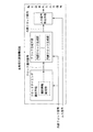
図16は、この種の半導体装置における入力インタフェース部の構成例を示している。図において、入力インタフェース部1は、複数の入力信号取込回路3を有している。
【0004】
各入力信号取込回路3には、それぞれ外部クロック信号CLKおよび入力信号Din(a)(またはDin(b))が入力されている。入力信号取込回路3からは、内部回路5に向けて、内部信号Doutz(a)・Doutx(a)(またはDoutz(b)・Doutx(b))が出力されている。なお、内部信号Doutzは、入力信号Dinと同相の信号であり、内部信号Doutxは入力信号Dinと逆相の信号である。
【0005】
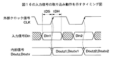
上述した入力信号取込回路3は、入力された入力信号Dinを、外部クロック信号CLKに同期して取り込み、内部信号Doutz、Doutxとして内部回路5に出力する。
図17は、図16に示した入力インタフェース部1における入力信号Dinの取り込みタイミングの一例を示している。この例では、入力信号Dinの入力期間は、外部クロック信号CLKの立ち上がりに対するセットアップ時間tDSおよびホールド時間tDHで規定されている。
【0006】
ここで、セットアップ時間tDSは、外部クロック信号CLKの立ち上がり以前に入力信号Dinの確定が必要な最小時間の規定であり、ホールド時間tDHは、外部クロック信号CLKの立ち上がり以後に入力信号Dinの保持が必要な最小時間の規定である。
そして、上記タイミング規定に従い入力信号Dinを入力することにより、入力信号Dinは、クロック信号CLKの立ち上がりで取り込まれ、内部信号Doutz、Doutxが生成される。
【0007】
ここで、セットアップ時間tDSおよびホールド時間tDHは、半導体製造工程で発生する半導体装置間での特性のばらつき、および、半導体装置を動作させる際の温度・電源電圧を考慮し、最悪の条件下でも確実に入力信号Dinを取り込むことができるように決められている。
【0008】
【発明が解決しようとする課題】
ところで、この種の半導体装置をシステム装置に搭載するユーザは、上述したように、半導体装置に入力する入力信号Dinをセットアップ時間tDSより前に確定させ、かつ、ホールド時間tDH以上保持するように、システム装置側のタイミング設計を行う必要がある。
【0009】
このため、システム装置上には、各入力信号Dinを作成するために、セットアップ時間tDSを満足させる回路と、ホールド時間tDHを満足させる回路とがそれぞれ必要になり、システム装置の回路規模が増大かつ複雑化していた。
さらに、動作周波数が100MHzを超えるような半導体装置の場合には、一般に、外部クロック信号CLKの周期は10ns以下になる。この結果、システム装置側のタイミング設計の余裕度は小さくなり、上述したタイミング規定に従って、入力信号Dinを作成することが難しかった。
【0010】
特に、入力信号Dinのセットアップ時間tDS側を確保するためには、1クロックサイクル手前の外部クロック信号CLKの立ち上がりまたは立ち下がりを使用しなくてはならず、外部クロック信号CLKの周期が短い場合には、このようなタイミング設計を行うことは、非常に難しかった。
【0011】
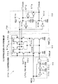
そこで、本発明者は、システム装置からは外部クロック信号の切替と同時に入力信号Dinを出力し、上記入力インタフェース部1において、外部クロック信号CLKに対して所定時間遅れたクロック信号を作成し、このクロック信号に同期して入力信号Dinを取り込むことを考察した。
図18は、本発明者により考察された入力インタフェース部1の構成を示している。図において、入力インタフェース部1は、上述した入力信号取込回路3およびインバータ7を有している。
【0012】
インバータ7は、外部クロック信号CLKを入力し、この外部クロック信号CLKの反転クロック信号/CLKを出力している。各入力信号取込回路3は、反転クロック信号/CLKを入力している。その他の構成は、図16に示したものと同一である。
図19は、図18に示した入力インタフェース部1における入力信号Dinの取り込みタイミングを示している。
【0013】
入力信号Dinは、反転クロック信号/CLKの立ち上がり(=外部クロック信号CLKの立ち下がり)で取り込まれる。この場合、入力信号Dinの入力期間は、反転クロック信号/CLKの立ち上がりに対するセットアップ時間tDS1およびホールド時間tDH1で規定される。
このため、外部クロック信号CLKの立ち上がりからデータが確定するまでの時間tDSを、外部クロック信号CLKの1/2周期より小さくできるときには、入力信号Dinの入力期間は、外部クロック信号CLKの立ち上がりに対するホールド時間tDHのみを満足すれば良いことになる。
【0014】
この結果、ユーザは、システム装置上で、入力信号Dinを外部クロック信号CLKの立ち上がりと同時に、もしくは、立ち上がりより後に発生させ、かつ、ホールド時間tDHだけ保持するようにタイミング設計を行えば良い。すなわち、タイミング設計を容易に行うことができる。
【0015】
図20は、本発明者が考察した別の入力インタフェース部1の構成を示している。図において、入力インタフェース部1は、上述した入力信号取込回路3および遅延回路9を有している。
遅延回路9は、外部クロック信号CLKを入力し、外部クロック信号CLKに対して所定時間遅延した遅延クロック信号DCLKを出力している。各入力信号取込回路3は遅延クロック信号DCLKを入力している。その他の構成は、図16に示したものと同一である。
【0016】
ここで、遅延回路9は、例えば、容量と抵抗とにより構成され、所定の時定数を有している。
図21は、図20に示した入力インタフェース部1における入力信号Dinの取り込みタイミングを示している。
入力信号Dinは、外部クロック信号CLKの立ち上がりから遅延時間Delayだけ遅れた遅延クロック信号DCLKの立ち上がりで取り込まれる。この場合、入力信号Dinの入力期間は、遅延クロック信号DCLKの立ち上がりに対するセットアップ時間tDS2およびホールド時間tDH2で規定される。
【0017】
このため、外部クロック信号CLKの立ち上がりからデータが確定するまでの時間tDSを、遅延時間Delayより小さくできるときには、入力信号Dinの入力期間は、外部クロック信号CLKの立ち上がりに対するホールド時間tDHのみを満足すれば良いことになる。
この結果、図18に示した入力インタフェース部1と同様に、ユーザは、システム装置上で、入力信号Dinを外部クロック信号CLKの立ち上がりと同時に、もしくは、立ち上がりより後に発生させ、かつ、ホールド時間tDHだけ保持するようにタイミング設計を行えば良い。すなわち、タイミング設計を容易に行うことができる。
【0018】
なお、上述した発明者による考察事項は、未だ公知にはなされていない。
しかしながら、図18に示したインバータ7を有する入力インタフェース部1では、外部クロック信号CLKを反転した反転クロック信号/CLKを使用して、入力信号Dinを取り込んでいるため、内部信号Doutz、Doutxを内部回路5に出力するタイミングが、外部クロック信号CLKの立ち上がりタイミングよりほぼ半クロック分遅くなる。
【0019】
このため、例えば、シンクロナスDRAM等のクロック同期型のメモリLSIにおけるアドレス信号・データ信号の取込部に本入力インタフェース部1を適用した場合には、読み出し時間、書き込み時間等のアクセス時間が、半クロック分遅くなる。
この遅れは、外部クロック信号CLKの周波数が高いときには、アクセス時間に与える影響は小さいが、外部クロック信号CLKの周波数が低くなるほど、アクセス時間に与える影響が大きくなるという問題があった。
【0020】
すなわち、このインタフェース部1を適用したメモリLSIのアクセス時間は、指定されたアドレスのメモリセルを選択し、選択されたメモリセルを外部に出力するまでに必要な時間と、外部クロック信号CLKの半クロック分の時間との和とほぼ等しくなる。前者の時間は、外部クロック信号CLKの周波数によらずほぼ一定であるが、後者の時間は、外部クロック信号CLKの周波数が低くなるにつれて長くなるため、外部クロック信号CLKの周期が長いときほど(=周波数が低いときほど)、アクセス時間に占める外部クロック信号CLKの半クロック分の時間の比率が大きくなり、アクセス時間に与える影響は大きくなる。
【0021】
一方、図20に示した遅延回路9を有する入力インタフェース部1では、外部クロック信号CLKを遅延した遅延クロック信号DCLKを使用して、入力信号Dinを取り込んでいる。
遅延回路9の遅延時間Delayは、半導体製造工程で生じる半導体装置間での特性のばらつき、および、半導体装置を動作させる際の温度・電源電圧等で変化し、この変化は外部クロック信号CLKの周波数には依存しない。
【0022】
このため、外部クロック信号CLKの周波数が高いほど、遅延時間Delayのばらつきの影響が大きく現れる。具体的には、例えば、遅延回路9の遅延時間Delayが2〜7nsにばらつく際に、外部クロック信号CLKの周波数が125MHz(クロック周期8ns)である場合には、遅延時間Delayの最大値とクロック周期との余裕は1nsしかなく、半導体装置内部のタイミング設計をおこなうことが困難になる。
【0023】
さらに、上述した不具合は、半導体装置を製造する際にも発生する。
すなわち、半導体装置の製造工程では、複数の半導体装置が形成されるウエハを1枚ずつ処理する枚葉処理工程と、複数のウエハを同時に処理するバッチ処理工程とがある。枚葉処理工程は、例えばホトリソグラフィ工程であり、バッチ処理工程は、例えば熱処理工程である。
【0024】
一般に、枚葉処理工程では、ウエハ上の半導体装置間の特性にばらつきが生じ易く、バッチ処理工程では、異なるウエハの半導体装置間の特性にばらつきが生じ易い。
複数の製造工程を経て、このようなばらつきが重ね合わせられる結果、製造された半導体装置の最高動作周波数のばらつきは、図22に示すように、中央にピークを有する山なりの分布を示す。
【0025】
そして、半導体装置は、ウエハ状態でのプローブ試験、組立後の選別試験により、例えば、最高動作周波数別に最速品・高速品・標準品の3種類に分けられれる。
この際、図18に示したインバータ7を有する入力インタフェース部1を半導体装置に適用した場合には、標準品において、アクセス時間に与える影響が大きくなり、アクセス時間が所定の時間を超える場合には、不良品になる。
【0026】
また、図20に示した遅延回路9を有する入力インタフェース部1を半導体装置に適用した場合には、最速品において、遅延時間Delayのばらつきの影響が大きくなり、内部回路5で内部信号Doutz、Doutxを取り込めない場合には、不良品になる。
【0027】
この結果、期待する歩留を得ることができず、半導体装置の製造コストが大幅に上昇する。
本発明は、かかる従来の問題点を解決するためになされたもので、外部クロック信号の周波数に拘わりなく、入力信号を確実に取り込むことができる半導体装置を提供することを目的とする。
【0028】
【課題を解決するための手段】
図1は、本発明の原理構成図である。
請求項1の半導体装置は、外部から入力される入力信号をクロック信号に同期して取り込む入力信号取込手段と、クロック選択信号を出力するクロックタイミング選択手段と、前記クロック選択信号および外部クロック信号を受けて、該クロック選択信号の信号値に応じた所定のタイミングの前記クロック信号を生成し、該クロック信号を前記入力信号取込手段に出力するクロック生成手段とを備え、前記クロック生成手段は、前記外部クロック信号とは位相が反転した内部クロック信号および前記外部クロック信号から所定時間遅れた内部クロック信号をそれぞれ生成する複数の内部クロック生成部を備え、前記クロック選択信号により選択された内部クロック信号を、前記クロック信号として前記入力信号取込手段に出力するように構成し、前記所定時間を、前記外部クロック信号のエッジから前記入力信号が示すデータが確定するまでの時間より大きくしたことを特徴とする。
【0030】
請求項2の半導体装置は、請求項1記載の半導体装置において、前記クロック生成手段は、前記外部クロック信号に対して位相が反転している反転内部クロック信号を生成する第1の内部クロック生成部と、遅延回路により遅延内部クロック信号を生成する第2の内部クロック生成部とを備え、前記クロック生成手段は、前記クロック選択信号が、一方の信号値であるときに前記クロック信号として前記反転内部クロック信号を出力し、他方の信号値であるときに前記クロック信号として前記遅延内部クロック信号を出力することを特徴とする。
【0031】
請求項3の半導体装置は、請求項1または請求項2記載の半導体装置において、前記クロックタイミング選択手段は、クロック選択情報を設定する選択情報設定部を備え、前記クロック選択信号は、前記選択情報設定部に設定された前記クロック選択情報に基づいて出力されることを特徴とする。
請求項4の半導体装置は、請求項3記載の半導体装置において、前記選択情報設定部は、外部から設定可能なレジスタにより構成され、前記クロックタイミング選択手段は、前記レジスタの記憶値に応じた信号値の前記クロック選択信号を出力することを特徴とする。
【0032】
請求項5の半導体装置は、請求項3記載の半導体装置において、前記選択情報設定部は、ヒューズにより構成され、前記クロックタイミング選択手段は、ヒューズの溶断の有無に応じた信号値の前記クロック選択信号を出力することを特徴とする。
請求項6の半導体装置は、請求項3記載の半導体装置において、前記選択情報設定部は、ボンディングパッドおよびボンディングワイヤにより構成され、前記クロックタイミング選択手段は、前記ボンディングパッドに接続される前記ボンディングワイヤに与えられた電圧値に応じた信号値の前記クロック選択信号を出力することを特徴とする。
【0033】
請求項7の半導体装置は、請求項3記載の半導体装置において、前記選択情報設定部は、半導体製造工程で使用するホトマスクのパターン形状に対応して半導体基板上の所定の位置に形成された導電膜により構成され、前記クロックタイミング選択手段は、前記導電膜の接続先の電圧値に応じた信号値の前記クロック選択信号を出力することを特徴とする。
【0034】
請求項8の半導体装置は、請求項1または請求項2記載の半導体装置において、前記クロックタイミング選択手段は、前記外部クロック信号の周波数を検出する周波数検出回路を備え、前記周波数検出回路は、検出した前記外部クロック信号の周波数に応じた前記クロック選択信号を出力することを特徴とする。
【0035】
請求項1の半導体装置では、クロックタイミング選択手段は、所定のクロック選択信号を出力する。
クロック生成手段は、クロック選択信号を受けて、このクロック選択信号の信号値に応じた所定のタイミングのクロック信号を生成する。
入力信号取込手段は、クロック生成手段から出力されたクロック信号に同期して、入力信号を取り込む。
【0036】
このため、入力信号取込手段は、使用する外部クロック信号の周波数等に応じて、最適なタイミングのクロック信号で入力信号(アドレス信号、データ信号等)を取り込むことができる。すなわち、外部クロック信号の周波数に拘わりなく、入力信号を確実に取り込むことができる。
また、クロック生成手段は、複数の内部クロック生成部を備え、各内部クロック生成部は、外部クロック信号とは位相が反転した、あるいは、外部クロック信号から所定時間遅れた内部クロック信号を生成する。
【0037】
入力信号取込手段は、選択された内部クロック信号を用いて入力信号を取り込む。
このため、入力取込手段は、外部クロック信号のエッジタイミングと同時に入力信号が入力された場合にも、入力信号を取り込むことが可能になる。
この結果、入力信号の入力タイミングの規定を緩和することが可能になり、本半導体装置を搭載するシステム装置のタイミング設計が容易になる。
【0038】
請求項2の半導体装置では、クロック生成手段は、クロック選択信号が一方の信号値であるときに、第1のクロック生成部を用いて、外部クロック信号に対して位相の反転した反転内部クロック信号を出力する。
また、クロック生成手段は、クロック選択信号が他方の信号値であるときに、第2のクロック生成部の遅延回路により、遅延内部クロック信号を生成し、出力する。
【0039】
このため、例えば、クロックタイミング選択手段により、外部クロック信号の周波数の高い・低いに応じて、クロック選択信号の信号値を一方・他方の値にすることで、入力信号取込手段は、外部クロック信号の周波数が高いときには、外部クロック信号の周期に依存する反転内部クロック信号で入力信号を取り込み、外部クロック信号の周波数が低いときには、外部クロック信号の周期に依存しない遅延内部クロック信号で入力信号を取り込むことができる。
【0040】
すなわち、入力信号取込手段は、外部クロック信号の周波数に応じて、最適かつ最速のタイミングで、入力信号を取り込むことができる。
請求項3の半導体装置では、選択情報設定部にクロック選択情報が設定され、クロックタイミング選択手段は、このクロック選択情報に基づいてクロック選択信号を出力する。
【0041】
このため、半導体装置を動作時に、予め、クロック選択情報を設定することができる。
請求項4の半導体装置では、選択情報設定部が、レジスタにより構成され、クロック選択情報の設定は、例えば、半導体装置を搭載するシステム装置上で、このレジスタをアクセスすることで行われる。
【0042】
この結果、半導体装置の動作時に、使用する外部クロック信号の周波数に応じて、選択情報を設定することができ、広範囲の動作周波数を有する半導体装置をユーザに提供することができる。
請求項5の半導体装置では、選択情報設定部が、ヒューズにより構成され、クロック選択情報の設定は、試験工程において、ヒューズを溶断・未溶断することで行われる。
【0043】
このため、例えば、プローブ試験で評価した最高動作周波数に応じてヒューズを溶断・未溶断することで、製造された半導体装置に最適なクロック選択情報が設定される。
請求項6の半導体装置では、選択情報設定部が、ボンディングパッドおよびボンディングワイヤにより構成され、クロック選択情報の設定は、組立行程において、ボンディングパッドに接続されるボンディングワイヤの接続先を変えることで行われる。
【0044】
請求項7の半導体装置では、選択情報設定部が、ホトマスクのパターン形状に対応して半導体基板上の所定の位置に形成された導電膜により構成され、クロック選択情報の設定は、半導体製造工程で使用するホトマスクの切り換えにより行われる。
クロック選択情報は、通常の半導体製造工程であるホトリソグラフィ工程およびエッチング工程中に設定されるため、特別な工程を設けることなく、クロック選択情報が設定される。
【0045】
請求項8の半導体装置では、クロックタイミング選択手段は、外部クロック信号の周波数を検出する周波数検出回路を備え、検出した周波数に応じたクロック選択信号を出力する。
このため、外部クロック信号の周波数に応じて、自動的に内部クロック信号が選択される。
【0046】
この結果、半導体製造工程では、クロック選択情報を設定することが不要になり、あるいは、半導体装置を搭載するシステム装置上では、クロック選択情報を設定することが不要になる。
【0047】
【発明の実施の形態】
以下、本発明をクロック同期型のメモリLSIに適用した例について、図面を用いて詳細に説明する。
【0048】
図2は、本発明の半導体装置の第1の実施形態(請求項1ないし請求項4に対応する)を示している。
図において、この実施形態の半導体装置100は、入出力インタフェース部200、メモリ制御インタフェース部300、およびメモリセルアレイ400により構成されている。
【0049】
入出力インタフェース部200には、外部クロック信号CLK、チップセレクト信号/CS、ライトイネーブル信号/WE等の制御信号、および、アドレス信号AD、データ信号DQが供給されている。なお、データ信号DQは入出力信号であり、データ信号DQ以外の信号は入力信号である。また、図において太い矢印で示したアドレス信号ADおよびデータ信号DQは複数本からなるバス信号である。
【0050】
これらの信号は、図示しないリードフレーム、ボンディングワイヤおよびボンディングパッドを介して、半導体装置100の外部から入出力インタフェース部200の各回路に接続されている。
入出力インターフェース200は、クロック制御部21、複数の入力バッファ23および出力バッファ25により構成されている。
【0051】
クロック制御部21は、外部クロック信号CLKを外部から入力し、図中破線で示した内部クロック信号INCLKを各入力バッファ23、出力バッファ25およびメモリ制御インタフェース部300に向けて出力している。
各入力バッファ23は、それぞれチップセレクト信号/CS、ライトイネーブル信号/WE、アドレス信号ADおよびデータ信号DQを外部から入力し、各信号に対応する内部信号Doutz、Doutxをメモリ制御インタフェース部300に向けて出力している。なお、内部信号Doutzは入力した信号と同相の信号であり、内部信号Doutxは入力した信号と逆相の信号である。
【0052】
出力バッファ25は、データ信号DQoutをメモリ制御インタフェース部300から入力し、データ信号DQを外部に向けて出力している。
メモリ制御インタフェース部300は、半導体装置100の動作モードを設定するモードレジスタ27(クロックタイミング選択手段、レジスタに対応する)および半導体装置100全体のタイミング制御等を行う複数の制御回路29により構成されている。
【0053】
モードレジスタ27は、クロック選択信号CLKSELを入出力インタフェース部200のクロック制御部21に向けて出力している。
また、メモリ制御インタフェース部300とメモリセルアレイ400との間には、制御信号31、行アドレス信号33、列アドレス信号35、I/O信号37が接続されている。
【0054】
メモリセルアレイ400には、図示しない複数のメモリセルが縦横に配列されている。この実施形態では、これ等メモリセルは、DRAMのメモリセルと同一ものが使用されており、一つのメモリセルは、一つのトランジスタと一つの容量とで構成されている。
なお、この実施形態の半導体装置100は、CMOS(Complementary MOS)プロセス技術を用いて製造されている。
【0055】
図3は、メモリ制御インタフェース部300のモードレジスタ27の回路構成を示している。
図において、モードレジスタ27は、制御回路39および複数のフリップフロップ回路41(0)〜41(n)(選択情報設定部に対応する)により構成されている。
制御回路39は、インバータ39aおよび2入力のNANDゲート39bにより構成されている。
【0056】
インバータ39aの入力には、ライトイネーブル信号/WEaが接続されており、インバータ39aの出力は、NANDゲート39bの一方の入力に接続されている。
NANDゲート39bの他方の入力には、チップセレクト信号/CSaが接続されており、NANDゲート39bの出力は、各フリップフロップ回路41(0)〜41(n)の入力に接続されている。
【0057】
チップセレクト信号/CSa、ライトイネーブル信号/WEaは、チップセレクト信号/CS、ライトイネーブル信号/WEから作成されたこれ等の信号と逆論理の信号である。
フロップ回路41(0)〜41(n)は、それぞれ1ビットの設定情報BIT0〜BITnを保持することができる。この実施形態では、モードレジスタ27の最下位ビットである設定情報BIT0は、クロック選択情報を保持するために使用されている。
【0058】
各フリップフロップ回路41(0)〜41(n)は、制御回路39の出力信号およびアドレス信号ADa0〜ADanを入力しており、設定情報BIT0〜BITnに対応した情報信号INF0〜INFnを出力している。なお、情報信号INF0は、クロック選択信号CLKSELとして使用されている。
このクロック選択信号CLKSELは、上述したように、入出力インタフェース部200のクロック制御部21に接続されている。
【0059】
また、アドレス信号ADa0〜ADanは、アドレス信号AD0〜ADnから作成されたこれ等の信号と同一論理の信号である。
フリップフロップ回路41(0)〜41(n)への情報の設定は、制御回路39の出力が低レベルのとき、すなわち、チップセレクト信号/CSaを高レベルにし、かつ、ライトイネーブル信号/WEaを低レベルにしたときに可能になる。
【0060】
そして、このときのアドレス信号ADa0〜ADanのレベルが、そのまま設定情報BIT0〜BITnとして設定され、設定した設定情報BIT0〜BITnが、情報信号INF0〜INFnとして出力される。
【0061】
この実施形態では、クロック選択信号CLKSELの出力値の設定は、半導体装置100を搭載するシステム装置側により行われる。一般には、システム装置のイニシャライズプログラムでこの設定が行われる。
モードレジスタ27の設定情報BIT0に設定する値は、外部クロック信号CLKの周波数が所定の値より高いときに「0」にされ、外部クロック信号CLKの周波数が所定の値より低いときに「1」にされる。
【0062】
そして、設定情報BIT0に「0」が設定された場合には、クロック選択信号CLKSELは低レベルになり、設定情報BIT0に「1」が設定された場合には、クロック選択信号CLKSELは高レベルになる。
図4は、クロック制御部21内に構成される内部クロック信号INCLKを生成するためのクロック生成回路21a(クロック生成手段に対応する)を示している。
【0063】
図において、クロック生成回路21aは、並列接続された第1の内部クロック生成部43と、第2の内部クロック生成部45とを備えている。
第1の内部クロック生成部43は、2入力のNORゲート43aの出力にインバータ43bを接続して構成されている。
第2の内部クロック生成部45は、2入力のNANDゲート45aの出力に、インバータ45b、遅延回路45c、インバータ45dを直列に接続して構成されている。
【0064】
遅延回路45cは、インバータ45bの出力に直列に接続される抵抗45e、および、この抵抗45eの出力端と接地VSSとの間を接続する容量45fにより構成されている。
ここで、例えば、抵抗45eは、n形拡散層を使用して形成され、容量45fは、NMOSトランジスタ(以下、NMOSと称する)を使用して形成されている。NMOSは、ゲート電極(以下、ゲートと称する)を抵抗45eの出力端に接続し、ソース電極(以下、ソースと称する)およびドレイン電極(以下、ドレインと称する)を接地VSSに接続して容量45fを構成している。
【0065】
また、第1の内部クロック生成部43のNORゲート43aおよび第2の内部クロック生成部45のNANDゲート45aの各入力には、それぞれ、外部クロック信号CLKおよびクロック選択信号CLKSELが接続されている。
第1の内部クロック生成部43のインバータ43bおよび第2の内部クロック生成部45のインバータ45dの出力は、2入力のNANDゲート47の入力に接続されている。そして、このNANDゲート47の出力は、内部クロック信号INCLKとして各回路に出力されている。
【0066】
図5は、入出力インタフェース部200の各入力バッファ23内に構成される入力信号取込回路23a(入力信号取込手段に対応する)の回路構成を示している。
図において、入力信号取込回路23aは、制御クロック作成部49、入力信号取込部51および内部信号出力部53により構成されている。
【0067】
制御クロック作成部49は、インバータとMOS容量とからなる二組の遅延回路55a、55bおよび2入力のNANDゲート57により構成されている。
遅延回路55a、55bは直列に接続され、遅延回路55bの出力はNANDゲート57の一方の入力に接続されている。NANDゲート57の他方の入力および遅延回路55aの入力には、内部クロック信号INCLKが接続されている。
【0068】
そして、NANDゲート57の出力は、反転信号/INCLKとなっている。また、入力信号取込部51は、複数のPMOSトランジスタ(以下、PMOSと称する)とNMOSとにより構成されており、内部クロック信号INCLK、反転信号/INCLK、入力信号Dinおよび参照信号Vrefを入力し、取込信号DO、/DOを出力している。取込信号DOは、入力信号Dinと同相の信号であり、取込信号/DOは、入力信号Dinと逆相の信号である。
【0069】
入力信号取込部51には、一つのPMOSと三つのNMOSとを直列に接続した比較回路59a、59bが対称に配置されている。これ等比較回路59a、59bは、入力信号Dinと参照信号Vrefとの電圧値の大小を比較し、入力信号Dinに対応する取込信号DO、/DOを発生する回路である。
また、取込信号DO、/DOには、入力と出力とを相互に接続した二つのCMOSインバータ61a、61bが接続されている。これ等CMOSインバータ61a、61bは、取込信号DO、/DOの電圧値を電源VCCまたは接地VSSまで増幅する回路である。
【0070】
さらに、入力信号取込部51は、比較回路59a、59bのノード59c、ノード59dをイコライズするNMOS59eを有している。
一方、内部信号出力部53は、PMOSおよびNMOSからなる二つの出力回路63a、63bと、各出力回路63a、63bのNMOSのゲートに接続され取込信号DO、/DOを入力するインバータ65a、65bと、出力回路から出力される内部信号Doutz、Doutxをラッチするために入力と出力とが相互に接続された二つのインバータ67a、67aとにより構成されている。
【0071】
上述した半導体装置では、モードレジスタ27の最下位ビットである設定情報BIT0に書き込まれたクロック選択情報により、以下示すように、クロック信号回路21aが動作し、入力信号取込回路23aにより入力信号Dinが取り込まれる。
なお、前述したように、クロック選択信号CLKSELの出力値の設定は、半導体装置100を搭載するシステム装置側により行われる。
【0072】
すなわち、先ず、モードレジスタ27の設定情報BIT0にクロック選択情報「0」を書き込んだ場合には、クロック選択信号CLKSELは低レベルになる。
この結果、図4に示したように、第1の内部クロック生成部43のNORゲート43aの出力には、外部クロック信号CLKと逆論理の信号が出力される。また、第2の内部クロック生成部45のNANDゲート45aの出力には、外部クロック信号CLKの論理値によらず高レベルが出力される。
【0073】
そして、NORゲート43aに出力された外部クロックCLKと逆論理の信号が、インバータ43bおよびNANDゲート47を通り、内部クロック信号INCLK(反転内部クロック信号に対応する)として出力される。
すなわち、クロック選択信号CLKSELを低レベルにすることで、第1の内部クロック生成部43が活性化され、外部クロック信号CLKに対して位相が反転した反転内部クロック信号が内部クロック信号INCLKとして出力される。このとき、第2の内部クロック生成部45は非活性状態にされている。
【0074】
この後、内部クロック信号INCLKは、図5に示したように、入力信号取込回路23aに入力される。
次に、モードレジスタ27の設定情報BIT0にクロック選択情報「1」を書き込んだ場合には、クロック選択信号CLKSELは高レベルになる。
この結果、第1の内部クロック生成部43のNORゲート43aの出力には、外部クロック信号CLKの論理値によらず低レベルが出力される。第2の内部クロック生成部45のNANDゲート45aの出力には、外部クロック信号CLKと逆論理の信号が出力される。
【0075】
そして、NANDゲート45aに出力された外部クロック信号CLKと逆論理の信号が、インバータ45b、遅延回路45c、インバータ45d、NANDゲート47を通り、外部クロック信号CLKに対して所定時間遅延した内部クロック信号INCLK(遅延内部クロック信号に対応する)として出力される。
すなわち、クロック選択信号CLKSELを高レベルにすることで、第2の内部クロック生成部45が活性化され、外部クロック信号CLKに対してほぼ遅延回路45cの遅延時間だけ遅れたタイミングの遅延内部クロック信号が内部クロック信号INCLKとして出力される。このとき、第1の内部クロック生成部43は非活性状態にされている。
【0076】
この後、内部クロック信号INCLKは、図5に示したように、入力信号取込回路23aに入力される。
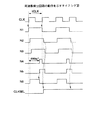
入力信号取込回路23aの制御クロック作成部49では、図6に示すように、内部クロック信号INCLKの立ち上がりタイミングを所定の時間だけ遅延させた反転信号/INCLKが作成される。
【0077】
また、入力信号取込部51は、内部クロック信号INCLK、反転信号/INCLKの状態により、次のように動作する。
先ず、内部クロック信号INCLKが低レベル、反転信号/INCLKが高レベルのときは、回路全体は非活性状態になり、取込信号DO、/DOは共に高レベルになる。
次に、内部クロック信号INCLK、反転信号/INCLKがともに高レベルになったときには、比較回路59a、59bは活性状態になる。比較回路59a、59bには、それぞれ入力信号Dinおよび参照信号Vrefの電圧に応じた電流が流れ、取込信号/DO、DOの電圧値が変化する。
【0078】
すなわち、内部クロック信号INCLKが高レベルになったときに、入力信号Dinの取り込みが開始される。
次に、内部クロック信号INCLKが高レベル、反転信号/INCLKが低レベルになったときには、CMOSインバータ61a、61bが活性化され、取込信号DO、/DOの電圧が増幅される。
【0079】
内部信号出力部53では、取込信号DO、/DOの電圧値に応じて、出力回路63a、63bが駆動される。そして、入力信号Dinに応じた内部信号Doutz、Doutxが出力される。
図7は、クロック選択信号CLKSELが低レベルである場合(外部クロック信号CLKの周波数が高い場合)の入力信号Dinの取込タイミングを示している。図において、内部クロック信号INCLKは、外部クロック信号CLKを反転した反転内部クロック信号である。
【0080】
入力信号Dinは、内部クロック信号INCLKの立ち上がり(=外部クロック信号CLKの立ち下がり)で取り込まれ、入力信号Dinに対応する内部信号Doutz、Doutxが出力される。
【0081】
入力信号Dinの入力期間は、前述した図19と同様に、内部クロック信号INCLKの立ち上がりに対するセットアップ時間tDS1およびホールド時間tDH1で規定される。
図8は、クロック選択信号CLKSELが高レベルである場合(外部クロック信号CLKの周波数が低い場合)の入力信号Dinの取込タイミングを示している。図において、内部クロック信号INCLKは、外部クロック信号CLKを遅延時間Delayだけ遅らせた遅延内部クロック信号である。
【0082】
入力信号Dinは、内部クロック信号INCLKの立ち上がりで取り込まれ、入力信号Dinに対応する内部信号Doutz、Doutxが出力される。
入力信号Dinの入力期間は、前述した図21と同様に、内部クロック信号INCLKの立ち上がりに対するセットアップ時間tDS2およびホールド時間tDH2で規定される。
【0083】
この実施形態では、図7および図8に示すように、セットアップ時間tDS1、tDS2の開始時間を、外部クロック信号CLKの立ち上がりより遅く設定している。この結果、入力信号Dinの入力期間は、外部クロック信号CLKの立ち上がりに対するホールド時間tDHのみで規定されている。
以上のように構成された半導体装置では、クロック生成回路21aにより、外部クロック信号CLKが所定の周波数より高いときに、外部クロック信号CLKの反転信号である内部クロック信号INCLK(反転内部クロック信号)を出力し、外部クロック信号CLKが所定の周波数より低いときに、外部クロック信号CLKから遅延時間Delayだけ遅らせた内部クロック信号INCLK(遅延内部クロック信号)を出力した。このため、入力信号取込回路23aは、外部クロック信号CLKの周波数が高いときには、外部クロック信号CLKの周期に依存する反転内部クロック信号で入力信号Dinを取り込み、外部クロック信号CLKの周波数が低いときには、外部クロック信号CLKの周期に依存しない遅延内部クロック信号で入力信号Dinを取り込むことができ、外部クロック信号CLKの周波数に応じて、最適かつ最速のタイミングで、入力信号Dinを取り込むことができる。
【0084】
この結果、外部クロック信号CLKの周波数が低い場合にも、アクセス時間に必要以上の遅れが発生することがなく、外部クロック信号CLKの周波数が高い場合にも、確実に入力信号Dinを取り込むことができる。
また、内部クロック信号INCLKの立ち上がりに対する入力信号Dinのセットアップ時間tDS1、tDS2の開始時間を、外部クロック信号CLKの立ち上がりより遅く設定した。
【0085】
このため、外部クロック信号CLKの立ち上がりと同時に入力信号Dinが入力された場合にも、入力信号Dinを確実に取り込むことができる。
そして、入力信号Dinの保持時間であるホールド時間tDHを考えるだけで良いため、入力タイミングの規定を、従来に比べ緩和することができる。
さらに、本半導体装置を搭載するシステム装置のタイミング設計が容易になり、システム装置の入力信号を出力するための回路が簡易化することが可能になる。
【0086】
すなわち、ユーザが使い易い半導体装置を構成することができる。
また、外部から書き込み可能なレジスタ27により、所定のレベルのクロック選択信号CLKSELを発生させたので、半導体装置の動作時に、クロック選択情報を設定することができる。
この結果、ユーザがシステム装置側からレジスタ27にデータを書き込むことで、クロック選択情報の設定を行うことができる。
【0087】
また、半導体装置側で、予めクロック選択信号CLKSELを設定する必要がないので、広範囲の周波数で動作可能な半導体装置をユーザに提供することができる。
図9は、本発明の半導体装置の第2の実施形態(請求項5に対応する)における選択情報設定部の一形態を示している。選択情報設定部以外の構成は、上述した第1の実施形態と同一である。
【0088】
図において、クロック選択信号CLKSELを出力とするインバータ71の入力には、ポリシリコン等からなるヒューズ73の一端およびn形拡散層等を使用して形成した抵抗75の一端が接続されている。ヒューズ73の他端および抵抗75の他端は、それぞれ電源VCCおよび接地VSSに接続されている。
抵抗75は、ヒューズ73が溶断されていないときの電源電流を極力小さくするために、高い抵抗値を有している。
【0089】
この実施形態の半導体装置では、半導体製造工程のプローブ試験において、半導体装置の最高動作周波数を評価し、ヒューズ73を溶断するか未溶断にするかが決められる。
すなわち、最高動作周波数が所定値以上である場合には、ヒューズ73を未溶断にする。このとき、インバータ71の入力には高レベルが入力され、クロック選択信号CLKSELは低レベルにされる。したがって、内部クロック信号INCLKは、外部クロック信号CLKの反転信号になる。
【0090】
一方、最高動作周波数が所定値未満である場合には、ヒューズ73を溶断する。このとき、インバータ71の入力には低レベルが入力され、クロック選択信号CLKSELは高レベルにされる。したがって、内部クロック信号INCLKは、外部クロック信号CLKに対して所定時間遅延した信号になる。
このため、半導体装置の動作周波数に応じた最適なタイミングの内部クロック信号INCLKが設定可能になる。
【0091】
この実施形態の半導体装置においても、上述した第1の実施形態と同様の効果を得ることができるが、この実施形態では、ヒューズ73の溶断・未溶断により、内部クロック信号INCLKのタイミングを変更する仕様としたので、プローブ試験等で評価した半導体装置の最高動作周波数に応じて、内部クロック信号INCLKのタイミングを設定することができる。
【0092】
また、製造工程の途中で、動作周波数に応じた最適なタイミングの内部クロック信号INCLKを選択することができるので、内部クロック信号INCLKが起因となる不良の発生率を低減することができ、歩留を向上することができる。この結果、製造コストを低減することができる。
図10は、本発明の半導体装置の第3の実施形態(請求項6に対応する)における選択情報設定部の一形態を示している。選択情報設定部以外の構成は、上述した第1の実施形態と同一である。
【0093】
図において、クロック選択信号CLKSELを出力とするインバータ77の入力には、ボンディングパッド79が接続されている。ボンディングパッド79に近接する位置には、電源VCCに接続されたボンディングパッド81と、接地VSSに接続されたボンディングパッド83とが配置されている。
この実施形態の半導体装置では、半導体製造工程のプローブ試験において、半導体装置の最高動作周波数を評価し、組立工程において、ボンディングパッド79をボンディングパッド81またはボンディングパッド83に接続する。
【0094】
すなわち、最高動作周波数が所定値以上である場合には、ボンディングワイヤ85により、ボンディングパッド79とボンディングパッド81とが接続される。このとき、クロック選択信号CLKSELは低レベルにされる。
一方、最高動作周波数が所定値未満である場合には、ボンディングワイヤ85により、ボンディングパッド79とボンディングパッド83とが接続される。このとき、クロック選択信号CLKSELは高レベルにされる。
【0095】
この実施形態の半導体装置においても、上述した第2の実施形態と同様の効果を得ることができる。
図11は、本発明の半導体装置の第4の実施形態(請求項7に対応する)における選択情報設定部の一形態を示している。選択情報設定部以外の構成は、上述した第1の実施形態と同一である。
【0096】
図において、クロック選択信号CLKSELを出力とするインバータ87の入力には、配線パターン89a、89b(導電膜に対応する)を介して、電源VCCまたは接地VSSが接続されている。
インバータ87の入力は、配線工程に使用するホトマスクのパターン形状により、電源VCCまたは接地VSSに接続される。
【0097】
すなわち、本実施形態では、配線工程において、パターン形状の異なる2枚のホトマスクが用意されている。そして、これ等ホトマスクのどちらか一方を使用して配線工程を行うことにより、配線パターン89aまたは配線パターン89bを介して、インバータ87の入力が電源VCCまたは接地VSSに接続される。
より具体的には、ホトリソグラフィ工程において、ホトマスクのパターン形状に対応するホトレジストパターンが半導体装置上に形成され、エッチング工程において、予め、スパッタリング等で形成された導電膜が、ホトレジストパターンにより選択的にエッチングされ、配線パターン89aまたは配線パターン89bが形成される。
【0098】
インバータ87の入力が電源VCCに接続された場合には、クロック選択信号CLKSELは低レベルになる。インバータ87の入力が接地VSSに接続された場合には、クロック選択信号CLKSELは高レベルになる。
なお、配線パターン89a、89bは、通常、インバータ87の入力から電源VCCまたは接地VSSまでの数十μm程度の配線で構成できるため、配線パターン89a、89bにより、半導体装置のチップ面積が増大することはない。
【0099】
この実施形態の半導体装置においても、上述した第2の実施形態と同様の効果を得ることができるが、この実施形態では、配線工程で使用するホトマスクを使用して、インバータ87の入力を電源VCCまたは接地VSSに接続したので、予め半導体装置の動作周波数毎の生産指示数量が分かっている際には、その生産指示数量に応じて、配線工程のホトマスクを切り換えることができる。
【0100】
また、ホトマスクにより配線パターン89を変更するだけで、クロック選択信号CLKSELのレベルを変えることができるので、半導体装置のチップ面積を増大することなく選択情報設定部を形成することができる。
そして、ホトマスクを変更する以外は、通常の半導体製造工程であるホトリソグラフィ工程およびエッチング工程を行うだけで、クロック選択信号CLKSELのレベルを変えることができ、特別な工程を設けることなく、クロック選択信号CLKSELの選択を行うことができる。
【0101】
図12は、本発明の半導体装置の第5の実施形態(請求項8に対応する)における周波数検出回路の一形態を示している。周波数検出回路(クロックタイミング選択手段)以外の構成は、上述した第1の実施形態と同一である。
図において、周波数検出回路90は、外部クロック信号CLKの周波数を半分にする1/2分周器91、入力した信号の立ち下がり側に正のパルス信号を発生させる遅延回路d1、所定の時定数を有する遅延回路d2、d3、RSフリップフロップ回路からなるラッチ部93、クロック選択信号CLKSELを出力するデータ転送部95により構成されている。
【0102】
1/2分周器91入力及び出力は、それぞれ、外部クロック信号CLKおよびノードN1に接続されている。
遅延回路d1は、2入力のNANDとインバータを直列に接続した複数の遅延段により構成されている。先頭の遅延段におけるNAND入力の一方には電源VCCが接続されている。各遅延段の出力は、接続先の遅延段のNAND入力の一方に接続されている。
【0103】
また、各遅延段のNAND入力の他方には、ノードN1が接続されている。遅延回路d1の出力は、ノードN4に接続されている。
遅延回路d2の入力および出力は、それぞれノードN1およびノードN2に接続されている。遅延回路d3の入力および出力は、それぞれノードN2およびノードN3に接続されている。
【0104】
ラッチ部93は、二つの2入力のNANDにより構成されている。ラッチ部93のリセット端子/Rには、ノードN3が接続され、セット端子/Sには、ノードN4の反転信号が接続されている。ラッチ93の出力Qは、ノードN5に接続されている。
データ転送部95は、PMOSとNMOSとのソース・ドレインを相互に接続したMOSスイッチ95a、95b、入力と出力とを相互に接続した二つのインバータ列95c、95d、MOSスイッチ95a、95bを制御するインバータ95eにより構成されている。
【0105】
そして、MOSスイッチ95a、インバータ列95c、MOSスイッチ95b、インバータ列95dが直列に接続されている。ここで、ノードN6は、インバータ列95cとMOSスイッチ95bとを接続しているノードである。
MOSスイッチ95aの入力側は、ノードN5に接続され、インバータ列95dの出力は、クロック選択信号CLKSELに接続されている。
【0106】
また、MOSスイッチ95aのNMOSのゲートおよびMOSスイッチ95bのPMOSのゲートは、ノードN2に接続されている。MOSスイッチ95aのPMOSのゲートおよびMOSスイッチ95bのNMOSのゲートは、ノードN2の反転信号に接続されている。
遅延回路d1は、ラッチ部93のセットタイミングを調整する回路である。遅延回路d2は、データ転送部95の転送データの取り込みタイミングを調整する回路である。
【0107】
図13および図14は、上述した周波数検出回路90の動作タイミングを示している。
ここで、外部クロック信号CLKの周期tCLKが、遅延回路d1の遅延時間delay1より長いとき、すなわち、外部クロック信号CLKの周波数が所定の値より低いときには、周波数検出回路は、図13に示すように動作する。
【0108】
先ず、1/2分周器91により、外部クロック信号CLKの周波数の半分の周波数の信号がノードN1に出力される。次に、遅延回路d2、d3により、ノードN1の信号から所定時間遅れた遅延信号がノードN2、N3に伝達される。
また、外部クロック信号CLKの周期tCLKは、遅延回路d1の遅延時間delay1より長いため、ノードN4には、ノードN1の立ち上がりから遅延時間delay1だけ遅れて正のパルスが発生する。
【0109】
ラッチ部93は、ノードN4のパルスを受けてノードN5を高レベルにする。ノードN5の高レベル状態は、ノードN3が低レベルになりラッチ部93がリセットされるまで維持される。
また、ノードN6は、ノードN5の高レベルを受けて低レベルになる。そして、ノードN2の立ち下がりエッジで、ノードN6の低レベル状態がラッチされる。
【0110】
同時に、インバータ列95dからノードN6の反転信号が出力され、クロック選択信号CLKSELが低レベルから高レベルに変化する。
この後、ノードN2の立ち下がりエッジ毎に、ノードN6の低レベル状態がラッチされ、クロック選択信号CLKSELは、常に高レベルを維持する。
この結果、外部クロック信号CLKの周期tCLKが遅延回路d1の遅延時間より長いときは、クロック選択信号CLKSELが高レベルになる。
【0111】
一方、外部クロック信号CLKの周期tCLKが、遅延回路d1の遅延時間delay1より短いとき、すなわち、外部クロック信号CLKの周波数が所定の値より高いときには、周波数検出回路は、図14に示すように動作する。
外部クロック信号CLKの周期tCLKが遅延回路d1の遅延時間より短いときには、ノードN4には正のパルスが発生しない。このため、ラッチ部93は、リセットされた状態を維持する。
【0112】
この結果、ノードN5は低レベルを維持し、クロック選択信号CLKSELは低レベルを維持する。
したがって、本実施形態では、外部クロック信号CLKの周波数に応じて、自動的にクロック選択信号CLKSELのレベルが変化する。そして、クロック選択信号CLKSELにより、最適なタイミングの内部クロックINCLKが選択される。
【0113】
この実施形態の半導体装置においても、上述した第1の実施形態と同様の効果を得ることができるが、この実施形態では、クロックタイミング選択手段に外部クロック信号CLKの周波数を検出する周波数検出回路90を備え、検出した周波数に応じたクロック選択信号CLKSELを出力したので、外部クロック信号CLKの周波数に応じて、自動的に最適な内部クロック信号INCLKを選択することができる。
【0114】
この結果、半導体製造工程において、クロック選択情報を設定することが不要になり、あるいは、半導体装置を搭載するシステム装置上で、クロック選択情報を設定することが不要になる。
また、半導体装置の動作時に、動作周波数に応じて自動的に内部クロック信号INCLKを選択できるので、予め、半導体製造工程において動作周波数を限定する必要がなくなり、動作周波数が広範囲にわたる半導体装置をユーザに提供することが可能になる。
【0115】
なお、上述した第1ないし第5の実施形態では、本発明をクロック同期型のメモリLSIに適用した例について述べたが、本発明はかかる実施形態に限定されるものではなく、例えば、マイクロコンピュータあるいはシステムLSI等に適用しても良い。特に、本発明は、外部クロック信号CLKに同期しない内部回路を有する半導体装置に適用する場合に効果を有する。
【0116】
また、上述した第1ないし第5の実施形態では、入力信号Dinの取り込みタイミングを、外部クロック信号CLKの立ち上がりに対するホールド時間tDHのみで規定した例について述べたが、本発明はかかる実施形態に限定されるものではなく、例えば、図15に示すように、さらに外部クロック信号CLKの立ち上がりに対するセットアップ時間tDSを規定しても良い。この場合には、半導体装置を搭載するシステム装置は、外部クロック信号CLKの立ち上がりに対して、ほぼ同時に入力信号Dinを発生させれば良いため、システム装置のタイミング設計が、さらに容易になる。
【0117】
そして、上述した第1ないし第5の実施形態では、クロック生成回路21aに、第1の内部クロック生成部43および第2の内部クロック生成部45を備えた例について述べたが、本発明はかかる実施形態に限定されるものではなく、例えば、三つ以上の内部クロック生成部を備え、複数のクロック選択情報と複数本のクロック選択信号とにより、内部クロック信号INCLKを生成しても良い。この場合には、より詳細なタイミングで、入力信号Dinを取り込むことができる。
【0118】
さらに、上述した第1ないし第5の実施形態では、抵抗45eをn形拡散層を使用して形成した例について述べたが、本発明はかかる実施形態に限定されるものではなく、例えば、p形拡散層を使用しても良く、ポリシリコン等の配線を使用しても良い。
また、上述した第3の実施形態では、ボンディングパッド79とボンディングパッド81またはボンディングパッド83とを接続した例について述べたが、本発明はかかる実施形態に限定されるものではなく、例えば、ボンディングパッド79を、ボンディングワイヤでリードフレームに直接接続しても良い。
【0119】
【発明の効果】
請求項1の半導体装置では、クロックタイミング選択手段が出力する所定のクロック選択信号に応じて、クロック生成手段は、所定のタイミングのクロック信号を生成し、入力信号取込手段は、このクロック信号に同期して入力信号を取り込んだので、使用する外部クロック信号の周波数等に応じて、最適なタイミングのクロック信号で、入力信号を取り込むことができる。すなわち、外部クロック信号の周波数に拘わりなく、入力信号を確実に取り込むことができる。
【0120】
また、外部クロック信号とは位相が反転した内部クロック信号あるいは外部クロックから所定時間遅れた内部クロック信号を用いて入力信号を取り込んだので、外部クロック信号のエッジタイミングと同時に入力信号が入力された場合にも、確実に入力信号を取り込むことができる。
【0121】
また、クロック生成手段は、クロック選択信号の信号値に基づいて、所定の内部クロック生成部を選択あるいは活性化するだけで、容易に、所定のタイミングの内部クロック信号を生成することができる。
請求項2の半導体装置では、クロック生成手段は、クロック選択信号の信号値に応じて、外部クロック信号に対して位相の反転した反転内部クロック信号または遅延内部クロック信号を生成し、出力したので、例えば、外部クロック信号の周波数が高いときには、外部クロック信号の周期に依存する反転内部クロック信号で入力信号を取り込み、外部クロック信号の周波数が低いときには、外部クロック信号の周期に依存しない遅延内部クロック信号で入力信号を取り込むことで、外部クロック信号の周波数に応じて、最適かつ最速のタイミングで、入力信号を取り込むことができる。
【0122】
請求項3の半導体装置では、クロック選択情報を設定する選択情報設定部を備えたので、半導体装置を動作させる以前に、予め、クロック選択情報を設定することができる。
請求項4の半導体装置では、選択情報設定部をレジスタにより構成したので、半導体装置の動作時に、使用する外部クロック信号の周波数に応じて、選択情報を設定することができる。
【0123】
請求項5の半導体装置では、選択情報設定部をヒューズにより構成したので、クロック選択情報の設定を、ヒューズを溶断・未溶断することで行うことができる。
このため、例えば、プローブ試験で評価した最高動作周波数に応じて、最適なクロック選択情報を設定することができる。
【0124】
請求項6の半導体装置では、選択情報設定部をボンディングパッドおよびボンディングワイヤにより構成したので、クロック選択情報の設定をボンディングパッドに接続されるボンディングワイヤの接続先を変えることで行うことができる。
このため、例えば、プローブ試験で評価した最高動作周波数に応じて、最適なクロック選択情報を設定することができる。
【0125】
請求項7の半導体装置では、選択情報設定部をホトマスクのパターン形状に対応して半導体基板上の所定の位置に形成される導電膜により構成したので、クロック選択情報の設定を、半導体製造工程で使用するホトマスクの切り換えにより行うことができる。
このため、クロック選択情報を、通常の半導体製造工程であるホトリソグラフィ工程およびエッチング工程中に設定することができ、特別な工程を設けることなく、クロック選択情報が設定することができる。
【0126】
請求項8の半導体装置では、クロックタイミング選択手段に、外部クロック信号の周波数を検出する周波数検出回路を備えたので、外部クロック信号の周波数に応じて、自動的に内部クロック信号を選択することができる。
この結果、半導体製造工程では、クロック選択情報を設定することが不要になり、あるいは、半導体装置を搭載するシステム装置上では、クロック選択情報を設定することが不要になる。
【0127】
したがって、外部クロック信号の周波数に拘わりなく、入力信号を確実に取り込むことができる。
【図面の簡単な説明】
【図1】 本発明の原理構成図である。
【図2】本発明の半導体装置の第1の実施形態を示す全体構成図である。
【図3】モードレジスタを示す回路構成図である。
【図4】クロック制御部におけるクロック生成回路を示す回路構成図である。
【図5】入力バッファにおける入力信号取込回路を示す回路構成図である。
【図6】内部クロック信号と内部クロック反転信号とを示すタイミング図である。
【図7】クロック選択信号の低レベル時における入力信号の取り込み動作を示すタイミング図である。
【図8】クロック選択信号の高レベル時における入力信号の取り込み動作を示すタイミング図である。
【図9】本発明の半導体装置の第2の実施形態における選択情報設定部の一形態を示す回路構成図である。
【図10】本発明の半導体装置の第3の実施形態における選択情報設定部の一形態を示す構成図である。
【図11】本発明の半導体装置の第4の実施形態における選択情報設定部の一形態を示す回路構成図である。
【図12】本発明の半導体装置の第5の実施形態における周波数検出回路の一形態を示す回路構成図である。
【図13】図12の周波数検出回路の動作を示すタイミング図である。
【図14】図12の周波数検出回路の別の動作を示すタイミング図である。
【図15】外部クロック信号CLKの立ち上がりに対するセットアップ時間tDSを規定した例を示すタイミング図である。
【図16】従来の半導体装置における入力インタフェース部を示す構成図である。
【図17】図16の入力インタフェース部における入力信号の取り込み動作を示すタイミング図である。
【図18】本発明者により考察された入力インタフェース部を示す構成図である。
【図19】図18の入力インタフェース部における入力信号の取り込み動作を示すタイミング図である。
【図20】本発明者により考察された別の入力インタフェース部を示す構成図である。
【図21】図20の入力インタフェース部における入力信号の取り込み動作を示すタイミング図である。
【図22】製造された複数の半導体装置の最高動作周波数のばらつきの例を示す説明図である。
【符号の説明】
21 クロック制御部
21a クロック生成回路(クロック生成手段)
23 入力バッファ
23a 入力信号取込回路(入力信号取込手段)
25 出力バッファ
27 モードレジスタ
29a、29b、29c 制御回路
31 制御信号
33 行アドレス信号
35 列アドレス信号
37 I/O信号
39 制御回路
39a インバータ
39b NANDゲート
41(0)〜41(n) フリップフロップ回路(選択情報設定部、記憶回路部)
43 第1の内部クロック生成部
43a NORゲート
43b インバータ
45 第2の内部クロック生成部
45a NANDゲート
45b、45d インバータ
45c 遅延回路
45e 抵抗
45f 容量
47 NANDゲート
49 制御クロック作成部
51 入力信号取込部
53 内部信号出力部
55a、55b 遅延回路
57 NANDゲート
59a、59b 比較回路
59c、59d ノード
59e NMOS
61a、61b CMOSインバータ
63a、63b 出力回路
65a、65b インバータ
67a、67b インバータ
71 インバータ
73 ヒューズ
75 抵抗
77 インバータ
79 ボンディングパッド
81、83 ボンディングパッド
85 ボンディングワイヤ
87 インバータ
89a、89b 配線パターン(導電膜)
91 1/2分周器
93 ラッチ部
95 データ転送部
95a、95b MOSスイッチ
95c、95d インバータ列
95e インバータ
100 半導体装置
200 入出力インタフェース部
300 メモリ制御インタフェース部
400 メモリセルアレイ
BIT0 設定情報(クロック選択情報)
CLK 外部クロック信号
CLKSEL クロック選択信号
Din 入力信号
INCLK 内部クロック信号[0001]
BACKGROUND OF THE INVENTION
The present invention relates to a clock synchronous semiconductor device that takes in an input signal input from the outside in synchronization with a clock signal.
[0002]
[Prior art]
In general, a semiconductor device such as an integrated circuit is roughly classified into a logic LSI such as a microcomputer and a memory LSI such as a DRAM (dynamic random access memory). Microcomputers are widely known as clock synchronous semiconductor devices. On the other hand, recently, a memory synchronous type such as a synchronous DRAM has been developed as a memory LSI.
[0003]
Synchronous DRAM enables data to be written and read at high speed by operating the interface circuit at high speed in synchronization with an external clock signal input from the outside. The maximum operating frequency is 100 MHz or higher. Things are being developed.
FIG. 16 shows a configuration example of an input interface unit in this type of semiconductor device. In the figure, the
[0004]
An external clock signal CLK and an input signal Din (a) (or Din (b)) are input to each input
[0005]
The input
FIG. 17 shows an example of the input signal Din capture timing in the
[0006]
Here, the setup time tDS is the minimum time required to determine the input signal Din before the rising edge of the external clock signal CLK, and the hold time tDH is the holding time of the input signal Din after the rising edge of the external clock signal CLK. This is the minimum time requirement.
Then, by inputting the input signal Din according to the timing specification, the input signal Din is captured at the rising edge of the clock signal CLK, and the internal signals Doutz and Doutx are generated.
[0007]
Here, the setup time tDS and hold time tDH are reliable even under worst-case conditions, taking into account variations in characteristics between semiconductor devices that occur in the semiconductor manufacturing process, and the temperature and power supply voltage when operating the semiconductor devices. It is determined so that the input signal Din can be taken in.
[0008]
[Problems to be solved by the invention]
By the way, as described above, the user who mounts this type of semiconductor device in the system device determines the input signal Din input to the semiconductor device before the set-up time tDS, and holds the hold time tDH or more. It is necessary to design the timing on the system unit side.
[0009]
For this reason, in order to create each input signal Din on the system device, a circuit that satisfies the setup time tDS and a circuit that satisfies the hold time tDH are required, which increases the circuit scale of the system device and It was complicated.
Furthermore, in the case of a semiconductor device whose operating frequency exceeds 100 MHz, the period of the external clock signal CLK is generally 10 ns or less. As a result, the timing design margin on the system device side is small, and it is difficult to create the input signal Din in accordance with the timing rules described above.
[0010]
In particular, in order to secure the setup time tDS side of the input signal Din, the rising or falling edge of the external clock signal CLK one clock cycle before must be used, and when the cycle of the external clock signal CLK is short It was very difficult to do such a timing design.
[0011]
Therefore, the present inventor outputs an input signal Din simultaneously with the switching of the external clock signal from the system device, and creates a clock signal delayed by a predetermined time with respect to the external clock signal CLK in the
FIG. 18 shows the configuration of the
[0012]
The
FIG. 19 shows the input signal Din capture timing in the
[0013]
The input signal Din is captured at the rising edge of the inverted clock signal / CLK (= the falling edge of the external clock signal CLK). In this case, the input period of the input signal Din is defined by the setup time tDS1 and hold time tDH1 with respect to the rising edge of the inverted clock signal / CLK.
For this reason, when the time tDS from the rising edge of the external clock signal CLK until the data is determined can be made smaller than a half cycle of the external clock signal CLK, the input period of the input signal Din is held for the rising edge of the external clock signal CLK. Only time tDH needs to be satisfied.
[0014]
As a result, the user may design the timing on the system device so that the input signal Din is generated simultaneously with or after the rising of the external clock signal CLK and is held for the hold time tDH. That is, the timing design can be easily performed.
[0015]
FIG. 20 shows a configuration of another
The
[0016]
Here, the
FIG. 21 shows the input signal Din capture timing in the
The input signal Din is captured at the rising edge of the delayed clock signal DCLK delayed by the delay time Delay from the rising edge of the external clock signal CLK. In this case, the input period of the input signal Din is defined by the setup time tDS2 and the hold time tDH2 with respect to the rising edge of the delayed clock signal DCLK.
[0017]
Therefore, when the time tDS from the rising edge of the external clock signal CLK until the data is determined can be made smaller than the delay time Delay, the input period of the input signal Din satisfies only the hold time tDH with respect to the rising edge of the external clock signal CLK. It will be good.
As a result, similar to the
[0018]
Note that the above-mentioned considerations by the inventors have not been made public.
However, since the
[0019]
For this reason, for example, when the
This delay has a small effect on the access time when the frequency of the external clock signal CLK is high, but has a problem that the effect on the access time increases as the frequency of the external clock signal CLK decreases.
[0020]
That is, the access time of the memory LSI to which the
[0021]
On the other hand, in the
The delay time Delay of the
[0022]
For this reason, the higher the frequency of the external clock signal CLK, the greater the influence of variations in the delay time Delay. Specifically, for example, when the delay time Delay of the
[0023]
Furthermore, the above-described problems also occur when manufacturing a semiconductor device.
That is, in the semiconductor device manufacturing process, there are a single wafer processing process in which wafers on which a plurality of semiconductor devices are formed one by one and a batch processing process in which a plurality of wafers are processed simultaneously. The single wafer processing process is, for example, a photolithography process, and the batch processing process is, for example, a heat treatment process.
[0024]
Generally, in the single wafer processing process, the characteristics between the semiconductor devices on the wafer are likely to vary. In the batch processing process, the characteristics between the semiconductor devices on different wafers are likely to vary.
As a result of such a variation being superimposed through a plurality of manufacturing steps, the variation in the maximum operating frequency of the manufactured semiconductor device shows a mountain-shaped distribution having a peak at the center as shown in FIG.
[0025]
The semiconductor devices are classified into, for example, the fastest product, the high-speed product, and the standard product according to the highest operating frequency by the probe test in the wafer state and the sorting test after assembly.
At this time, when the
[0026]
In addition, when the
[0027]
As a result, the expected yield cannot be obtained, and the manufacturing cost of the semiconductor device increases significantly.
The present invention has been made to solve such a conventional problem, and an object of the present invention is to provide a semiconductor device that can reliably take in an input signal regardless of the frequency of an external clock signal.
[0028]
[Means for Solving the Problems]
FIG. 1 is a principle configuration diagram of the present invention.
3. The semiconductor device according to
[0030]
[0031]
[0032]
[0033]
[0034]
[0035]
According to another aspect of the semiconductor device of the present invention, the clock timing selection means outputs a predetermined clock selection signal.
The clock generation means receives the clock selection signal and generates a clock signal at a predetermined timing according to the signal value of the clock selection signal.
The input signal capture means captures the input signal in synchronization with the clock signal output from the clock generation means.
[0036]
For this reason, the input signal capturing means can capture the input signal (address signal, data signal, etc.) with the clock signal at the optimum timing according to the frequency of the external clock signal to be used. That is, the input signal can be reliably captured regardless of the frequency of the external clock signal.
Also, The clock generation means includes a plurality of internal clock generation units, and each internal clock generation unit generates an internal clock signal whose phase is inverted from that of the external clock signal or delayed by a predetermined time from the external clock signal.
[0037]
The input signal capturing means captures an input signal using the selected internal clock signal.
For this reason, the input capturing means can capture the input signal even when the input signal is input simultaneously with the edge timing of the external clock signal.
As a result, it becomes possible to relax the input timing definition of the input signal, and the timing design of the system device mounting the semiconductor device is facilitated.
[0038]
The clock generation means generates and outputs a delayed internal clock signal by the delay circuit of the second clock generation unit when the clock selection signal has the other signal value.
[0039]
For this reason, for example, the clock signal selection means changes the signal value of the clock selection signal to one or the other value according to the high or low frequency of the external clock signal, so that the input signal capturing means When the frequency of the signal is high, the input signal is captured with an inverted internal clock signal that depends on the period of the external clock signal. When the frequency of the external clock signal is low, the input signal is input with a delayed internal clock signal that does not depend on the period of the external clock signal. Can be captured.
[0040]
In other words, the input signal capturing means can capture the input signal at the optimum and fastest timing according to the frequency of the external clock signal.
[0041]
Therefore, clock selection information can be set in advance when operating the semiconductor device.
[0042]
As a result, selection information can be set according to the frequency of the external clock signal to be used during operation of the semiconductor device, and a semiconductor device having a wide range of operating frequencies can be provided to the user.
[0043]
For this reason, for example, the optimal clock selection information for the manufactured semiconductor device is set by blowing or not blowing the fuse according to the maximum operating frequency evaluated in the probe test.
[0044]
Since the clock selection information is set during a photolithography process and an etching process, which are normal semiconductor manufacturing processes, the clock selection information is set without providing a special process.
[0045]
Therefore, the internal clock signal is automatically selected according to the frequency of the external clock signal.
[0046]
As a result, it is not necessary to set clock selection information in the semiconductor manufacturing process, or it is not necessary to set clock selection information on a system device on which the semiconductor device is mounted.
[0047]
DETAILED DESCRIPTION OF THE INVENTION
Hereinafter, an example in which the present invention is applied to a clock synchronous memory LSI will be described in detail with reference to the drawings.
[0048]
FIG. 2 shows a first embodiment of a semiconductor device according to the present invention.
In the figure, a
[0049]
The input /
[0050]
These signals are connected to each circuit of the input /
The input /
[0051]
The clock control unit 21 receives an external clock signal CLK from the outside, and outputs an internal clock signal INCLK indicated by a broken line in the drawing to each
Each
[0052]
The
The memory
[0053]
The
A control signal 31, a
[0054]
In the
The
[0055]
FIG. 3 shows a circuit configuration of the
In the figure, the
The
[0056]
A write enable signal / WEa is connected to the input of the inverter 39a, and the output of the inverter 39a is connected to one input of the NAND gate 39b.
The other input of the NAND gate 39b is connected to the chip select signal / CSa, and the output of the NAND gate 39b is connected to the inputs of the flip-flop circuits 41 (0) to 41 (n).
[0057]
The chip select signal / CSa and the write enable signal / WEa are signals having a logic opposite to those generated from the chip select signal / CS and the write enable signal / WE.
The flop circuits 41 (0) to 41 (n) can hold 1-bit setting information BIT0 to BITn, respectively. In this embodiment, the setting information BIT0 that is the least significant bit of the
[0058]
Each flip-flop circuit 41 (0) to 41 (n) receives the output signal of the
The clock selection signal CLKSEL is connected to the clock control unit 21 of the input /
[0059]
The address signals ADa0 to ADan are signals having the same logic as these signals generated from the address signals AD0 to ADn.
Information is set in the flip-flop circuits 41 (0) to 41 (n) when the output of the
[0060]
The levels of the address signals ADa0 to ADan at this time are set as setting information BIT0 to BITn as they are, and the set setting information BIT0 to BITn are output as information signals INF0 to INFn.
[0061]
In this embodiment, the output value of the clock selection signal CLKSEL is set by the system device on which the
The value set in the setting information BIT0 of the
[0062]
When the setting information BIT0 is set to “0”, the clock selection signal CLKSEL is at a low level. When the setting information BIT0 is set to “1”, the clock selection signal CLKSEL is at a high level. Become.
FIG. 4 shows a clock generation circuit 21a (corresponding to clock generation means) for generating an internal clock signal INCLK configured in the clock control unit 21.
[0063]
In the figure, the clock generation circuit 21 a includes a first internal clock generation unit 43 and a second internal
The first internal clock generator 43 is configured by connecting an
The second internal
[0064]
The delay circuit 45c includes a resistor 45e connected in series to the output of the inverter 45b, and a
Here, for example, the resistor 45e is formed using an n-type diffusion layer, and the
[0065]
The external clock signal CLK and the clock selection signal CLKSEL are connected to the inputs of the NOR gate 43a of the first internal clock generation unit 43 and the NAND gate 45a of the second internal
The outputs of the
[0066]
FIG. 5 shows a circuit configuration of an input signal capturing circuit 23a (corresponding to input signal capturing means) configured in each
In the figure, the input signal capturing circuit 23 a includes a control
[0067]
The control
The delay circuits 55 a and 55 b are connected in series, and the output of the delay circuit 55 b is connected to one input of the
[0068]
The output of the
[0069]
In the input signal capturing unit 51, comparison circuits 59a and 59b in which one PMOS and three NMOSs are connected in series are arranged symmetrically. These comparison circuits 59a and 59b are circuits that compare the magnitudes of the voltage values of the input signal Din and the reference signal Vref and generate the capture signals DO and / DO corresponding to the input signal Din.
In addition, two CMOS inverters 61a and 61b in which inputs and outputs are connected to each other are connected to the capture signals DO and / DO. These CMOS inverters 61a and 61b are circuits that amplify the voltage values of the capture signals DO and / DO up to the power supply VCC or the ground VSS.
[0070]
Further, the input signal capturing unit 51 includes an NMOS 59e that equalizes the nodes 59c and 59d of the comparison circuits 59a and 59b.
On the other hand, the internal
[0071]
In the semiconductor device described above, the clock signal circuit 21a operates as shown below by the clock selection information written in the setting information BIT0 which is the least significant bit of the
As described above, the setting of the output value of the clock selection signal CLKSEL is performed by the system device on which the
[0072]
That is, first, when the clock selection information “0” is written in the setting information BIT0 of the
As a result, as shown in FIG. 4, a signal having a logic opposite to that of the external clock signal CLK is output to the output of the NOR gate 43a of the first internal clock generator 43. Further, a high level is output to the output of the NAND gate 45a of the second internal
[0073]
Then, a signal having a logic opposite to that of the external clock CLK output to the NOR gate 43a is output as an internal clock signal INCLK (corresponding to an inverted internal clock signal) through the
That is, by setting the clock selection signal CLKSEL to a low level, the first internal clock generation unit 43 is activated, and an inverted internal clock signal whose phase is inverted with respect to the external clock signal CLK is output as the internal clock signal INCLK. The At this time, the second
[0074]
Thereafter, the internal clock signal INCLK is input to the input signal capturing circuit 23a as shown in FIG.
Next, when the clock selection information “1” is written in the setting information BIT0 of the
As a result, a low level is output to the output of the NOR gate 43a of the first internal clock generation unit 43 regardless of the logical value of the external clock signal CLK. A signal having a logic opposite to that of the external clock signal CLK is output to the output of the NAND gate 45 a of the second internal
[0075]
Then, an internal clock signal obtained by delaying the external clock signal CLK output to the NAND gate 45a by a predetermined time with respect to the external clock signal CLK through the inverter 45b, the delay circuit 45c, the
That is, by setting the clock selection signal CLKSEL to a high level, the second internal
[0076]
Thereafter, the internal clock signal INCLK is input to the input signal capturing circuit 23a as shown in FIG.
As shown in FIG. 6, the
[0077]
Further, the input signal capturing unit 51 operates as follows according to the states of the internal clock signal INCLK and the inverted signal / INCLK.
First, when the internal clock signal INCLK is at a low level and the inverted signal / INCLK is at a high level, the entire circuit is inactivated, and both the capture signals DO and / DO are at a high level.
Next, when both the internal clock signal INCLK and the inverted signal / INCLK become high level, the comparison circuits 59a and 59b are activated. Currents corresponding to the voltages of the input signal Din and the reference signal Vref flow through the comparison circuits 59a and 59b, respectively, and the voltage values of the acquisition signals / DO and DO change.
[0078]
That is, when the internal clock signal INCLK becomes high level, the input signal Din is started to be captured.
Next, when the internal clock signal INCLK is at a high level and the inverted signal / INCLK is at a low level, the CMOS inverters 61a and 61b are activated, and the voltages of the capture signals DO and / DO are amplified.
[0079]
In the internal
FIG. 7 shows the capture timing of the input signal Din when the clock selection signal CLKSEL is at a low level (when the frequency of the external clock signal CLK is high). In the figure, the internal clock signal INCLK is an inverted internal clock signal obtained by inverting the external clock signal CLK.
[0080]
The input signal Din is captured at the rising edge of the internal clock signal INCLK (= the falling edge of the external clock signal CLK), and the internal signals Doutz and Doutx corresponding to the input signal Din are output.
[0081]
The input period of the input signal Din is defined by the setup time tDS1 and hold time tDH1 with respect to the rising edge of the internal clock signal INCLK, as in FIG.
FIG. 8 shows the input timing of the input signal Din when the clock selection signal CLKSEL is at a high level (when the frequency of the external clock signal CLK is low). In the figure, an internal clock signal INCLK is a delayed internal clock signal obtained by delaying the external clock signal CLK by a delay time Delay.
[0082]
The input signal Din is captured at the rising edge of the internal clock signal INCLK, and the internal signals Doutz and Doutx corresponding to the input signal Din are output.
The input period of the input signal Din is defined by the setup time tDS2 and hold time tDH2 with respect to the rising edge of the internal clock signal INCLK, as in FIG.
[0083]
In this embodiment, as shown in FIGS. 7 and 8, the start times of the setup times tDS1 and tDS2 are set later than the rising edge of the external clock signal CLK. As a result, the input period of the input signal Din is defined only by the hold time tDH with respect to the rising edge of the external clock signal CLK.
In the semiconductor device configured as described above, when the external clock signal CLK is higher than a predetermined frequency, the clock generation circuit 21a generates an internal clock signal INCLK (inverted internal clock signal) that is an inverted signal of the external clock signal CLK. When the external clock signal CLK is lower than a predetermined frequency, the internal clock signal INCLK (delayed internal clock signal) delayed from the external clock signal CLK by the delay time Delay is output. Therefore, when the frequency of the external clock signal CLK is high, the input signal capturing circuit 23a takes in the input signal Din with an inverted internal clock signal that depends on the period of the external clock signal CLK, and when the frequency of the external clock signal CLK is low The input signal Din can be captured by a delayed internal clock signal that does not depend on the cycle of the external clock signal CLK, and the input signal Din can be captured at the optimum and fastest timing according to the frequency of the external clock signal CLK.
[0084]
As a result, even when the frequency of the external clock signal CLK is low, the access time is not delayed more than necessary, and the input signal Din can be reliably captured even when the frequency of the external clock signal CLK is high. it can.
In addition, the setup time tDS1 and tDS2 of the input signal Din relative to the rising edge of the internal clock signal INCLK is set later than the rising edge of the external clock signal CLK.
[0085]
Therefore, even when the input signal Din is input simultaneously with the rising edge of the external clock signal CLK, the input signal Din can be reliably captured.
Since only the hold time tDH, which is the hold time of the input signal Din, needs to be considered, the input timing can be relaxed compared to the conventional case.
Furthermore, the timing design of the system device on which the semiconductor device is mounted is facilitated, and the circuit for outputting the input signal of the system device can be simplified.
[0086]
That is, it is possible to configure a semiconductor device that is easy for the user to use.
Further, since the clock selection signal CLKSEL of a predetermined level is generated by the
As a result, the user can set the clock selection information by writing data to the
[0087]
Further, since it is not necessary to set the clock selection signal CLKSEL in advance on the semiconductor device side, a semiconductor device that can operate over a wide range of frequencies can be provided to the user.
FIG. 9 shows a second embodiment of a semiconductor device of the present invention (
[0088]
In the figure, an input of an inverter 71 that outputs a clock selection signal CLKSEL is connected to one end of a fuse 73 made of polysilicon or the like and one end of a
The
[0089]
In the semiconductor device of this embodiment, in the probe test of the semiconductor manufacturing process, the maximum operating frequency of the semiconductor device is evaluated, and it is determined whether the fuse 73 is blown or not blown.
That is, when the maximum operating frequency is equal to or higher than the predetermined value, the fuse 73 is not blown. At this time, a high level is input to the input of the inverter 71, and the clock selection signal CLKSEL is set to a low level. Therefore, the internal clock signal INCLK becomes an inverted signal of the external clock signal CLK.
[0090]
On the other hand, if the maximum operating frequency is less than the predetermined value, the fuse 73 is blown. At this time, a low level is input to the input of the inverter 71, and the clock selection signal CLKSEL is set to a high level. Therefore, the internal clock signal INCLK is a signal delayed by a predetermined time with respect to the external clock signal CLK.
Therefore, it is possible to set the internal clock signal INCLK at an optimal timing according to the operating frequency of the semiconductor device.
[0091]
Even in the semiconductor device of this embodiment, the same effect as that of the first embodiment described above can be obtained, but in this embodiment, the timing of the internal clock signal INCLK is changed depending on whether the fuse 73 is blown or not blown. Since the specification is adopted, the timing of the internal clock signal INCLK can be set according to the maximum operating frequency of the semiconductor device evaluated by a probe test or the like.
[0092]
In addition, since the internal clock signal INCLK having the optimal timing according to the operating frequency can be selected during the manufacturing process, the occurrence rate of defects caused by the internal clock signal INCLK can be reduced, and the yield can be reduced. Can be improved. As a result, the manufacturing cost can be reduced.
FIG. 10 shows a third embodiment of a semiconductor device of the present invention (
[0093]
In the figure, a bonding pad 79 is connected to an input of an
In the semiconductor device of this embodiment, the maximum operating frequency of the semiconductor device is evaluated in the probe test of the semiconductor manufacturing process, and the bonding pad 79 is connected to the bonding pad 81 or the bonding pad 83 in the assembly process.
[0094]
That is, when the maximum operating frequency is a predetermined value or more, the bonding pad 79 and the bonding pad 81 are connected by the bonding wire 85. At this time, the clock selection signal CLKSEL is set to a low level.
On the other hand, when the maximum operating frequency is less than the predetermined value, the bonding pad 79 and the bonding pad 83 are connected by the bonding wire 85. At this time, the clock selection signal CLKSEL is set to a high level.
[0095]
Also in the semiconductor device of this embodiment, the same effect as that of the second embodiment described above can be obtained.
FIG. 11 shows a semiconductor device according to a fourth embodiment (
[0096]
In the figure, an input of an
The input of the
[0097]
That is, in this embodiment, two photomasks having different pattern shapes are prepared in the wiring process. Then, by performing a wiring process using one of these photomasks, the input of the
More specifically, in the photolithography process, a photoresist pattern corresponding to the pattern shape of the photomask is formed on the semiconductor device, and in the etching process, the conductive film previously formed by sputtering or the like is selectively formed by the photoresist pattern. The wiring pattern 89a or the wiring pattern 89b is formed by etching.
[0098]
When the input of the
Note that the wiring patterns 89a and 89b can usually be configured with wiring of about several tens of μm from the input of the
[0099]
In the semiconductor device of this embodiment, the same effect as that of the second embodiment described above can be obtained. In this embodiment, the input of the
[0100]
Further, since the level of the clock selection signal CLKSEL can be changed simply by changing the wiring pattern 89 using a photomask, the selection information setting unit can be formed without increasing the chip area of the semiconductor device.
The level of the clock selection signal CLKSEL can be changed by performing only the photolithography process and the etching process, which are normal semiconductor manufacturing processes, except for changing the photomask, and without providing a special process. CLKSEL can be selected.
[0101]
FIG. 12 shows a semiconductor device according to a fifth embodiment (
In the figure, a frequency detection circuit 90 includes a 1/2
[0102]
The 1/2
The delay circuit d1 includes a plurality of delay stages in which a two-input NAND and an inverter are connected in series. A power supply VCC is connected to one of the NAND inputs in the first delay stage. The output of each delay stage is connected to one of the NAND inputs of the connected delay stages.
[0103]
A node N1 is connected to the other NAND input of each delay stage. The output of the delay circuit d1 is connected to the node N4.
The input and output of the delay circuit d2 are connected to the node N1 and the node N2, respectively. The input and output of the delay circuit d3 are connected to the node N2 and the node N3, respectively.
[0104]
The
The
[0105]
A MOS switch 95a, an inverter array 95c, a MOS switch 95b, and an inverter array 95d are connected in series. Here, the node N6 is a node connecting the inverter train 95c and the MOS switch 95b.
The input side of the MOS switch 95a is connected to the node N5, and the output of the inverter train 95d is connected to the clock selection signal CLKSEL.
[0106]
The NMOS gate of the MOS switch 95a and the PMOS gate of the MOS switch 95b are connected to the node N2. The PMOS gate of the MOS switch 95a and the NMOS gate of the MOS switch 95b are connected to the inverted signal of the node N2.
The delay circuit d <b> 1 is a circuit that adjusts the set timing of the
[0107]
13 and 14 show the operation timing of the frequency detection circuit 90 described above.
Here, when the cycle tCLK of the external clock signal CLK is longer than the delay time delay1 of the delay circuit d1, that is, when the frequency of the external clock signal CLK is lower than a predetermined value, the frequency detection circuit is as shown in FIG. Operate.
[0108]
First, the ½
Further, since the cycle tCLK of the external clock signal CLK is longer than the delay time delay1 of the delay circuit d1, a positive pulse is generated at the node N4 with a delay time delay1 from the rise of the node N1.
[0109]
The
Further, the node N6 becomes low level in response to the high level of the node N5. Then, the low level state of the node N6 is latched at the falling edge of the node N2.
[0110]
At the same time, an inverted signal of the node N6 is output from the inverter train 95d, and the clock selection signal CLKSEL changes from the low level to the high level.
Thereafter, at every falling edge of the node N2, the low level state of the node N6 is latched, and the clock selection signal CLKSEL always maintains the high level.
As a result, when the cycle tCLK of the external clock signal CLK is longer than the delay time of the delay circuit d1, the clock selection signal CLKSEL becomes high level.
[0111]
On the other hand, when the cycle tCLK of the external clock signal CLK is shorter than the delay time delay1 of the delay circuit d1, that is, when the frequency of the external clock signal CLK is higher than a predetermined value, the frequency detection circuit operates as shown in FIG. To do.
When the period tCLK of the external clock signal CLK is shorter than the delay time of the delay circuit d1, no positive pulse is generated at the node N4. For this reason, the
[0112]
As a result, the node N5 maintains a low level, and the clock selection signal CLKSEL maintains a low level.
Therefore, in the present embodiment, the level of the clock selection signal CLKSEL automatically changes according to the frequency of the external clock signal CLK. Then, the internal clock INCLK having the optimum timing is selected by the clock selection signal CLKSEL.
[0113]
In the semiconductor device of this embodiment, the same effect as that of the first embodiment described above can be obtained, but in this embodiment, the frequency detection circuit 90 detects the frequency of the external clock signal CLK in the clock timing selection means. Since the clock selection signal CLKSEL corresponding to the detected frequency is output, the optimum internal clock signal INCLK can be automatically selected according to the frequency of the external clock signal CLK.
[0114]
As a result, it is not necessary to set clock selection information in the semiconductor manufacturing process, or it is not necessary to set clock selection information on the system device on which the semiconductor device is mounted.
In addition, since the internal clock signal INCLK can be automatically selected according to the operating frequency during the operation of the semiconductor device, there is no need to limit the operating frequency in the semiconductor manufacturing process in advance, and a semiconductor device with a wide operating frequency can be used by the user. It becomes possible to provide.
[0115]
In the first to fifth embodiments described above, examples in which the present invention is applied to a clock synchronous memory LSI have been described. However, the present invention is not limited to such embodiments, and for example, a microcomputer. Alternatively, it may be applied to a system LSI or the like. In particular, the present invention is effective when applied to a semiconductor device having an internal circuit that is not synchronized with the external clock signal CLK.
[0116]
In the first to fifth embodiments described above, the example in which the input signal Din capturing timing is defined only by the hold time tDH with respect to the rising edge of the external clock signal CLK has been described. However, the present invention is limited to such an embodiment. For example, as shown in FIG. 15, a setup time tDS for the rising edge of the external clock signal CLK may be further defined. In this case, since the system device on which the semiconductor device is mounted has only to generate the input signal Din almost simultaneously with the rising edge of the external clock signal CLK, the timing design of the system device is further facilitated.
[0117]
In the first to fifth embodiments described above, the example in which the clock generation circuit 21a includes the first internal clock generation unit 43 and the second internal
[0118]
Furthermore, in the first to fifth embodiments described above, the example in which the resistor 45e is formed using the n-type diffusion layer has been described. However, the present invention is not limited to such an embodiment. A shaped diffusion layer may be used, and wiring such as polysilicon may be used.
In the third embodiment described above, an example in which the bonding pad 79 and the bonding pad 81 or the bonding pad 83 are connected has been described. However, the present invention is not limited to such an embodiment. 79 may be directly connected to the lead frame with a bonding wire.
[0119]
【The invention's effect】
According to another aspect of the semiconductor device of the present invention, the clock generation unit generates a clock signal having a predetermined timing in response to the predetermined clock selection signal output from the clock timing selection unit, and the input signal fetching unit Since the input signal is captured in synchronism, the input signal can be captured with a clock signal having an optimal timing in accordance with the frequency of the external clock signal used. That is, the input signal can be reliably captured regardless of the frequency of the external clock signal.
[0120]
Also, The external clock signal is input using the internal clock signal whose phase is inverted or the internal clock signal delayed by a predetermined time from the external clock, so even when the input signal is input simultaneously with the edge timing of the external clock signal The input signal can be surely captured.
[0121]
In addition, the clock generation means can easily generate an internal clock signal at a predetermined timing simply by selecting or activating a predetermined internal clock generation unit based on the signal value of the clock selection signal.
[0122]
[0123]
Therefore, for example, optimal clock selection information can be set according to the maximum operating frequency evaluated in the probe test.
[0124]
Therefore, for example, optimal clock selection information can be set according to the maximum operating frequency evaluated in the probe test.
[0125]
Therefore, the clock selection information can be set during a photolithography process and an etching process, which are normal semiconductor manufacturing processes, and the clock selection information can be set without providing a special process.
[0126]
As a result, it is not necessary to set clock selection information in the semiconductor manufacturing process, or it is not necessary to set clock selection information on a system device on which the semiconductor device is mounted.
[0127]
Therefore, the input signal can be reliably captured regardless of the frequency of the external clock signal.
[Brief description of the drawings]
[Figure 1] The present invention FIG.
FIG. 2 is an overall configuration diagram showing a first embodiment of a semiconductor device of the present invention.
FIG. 3 is a circuit configuration diagram showing a mode register.
FIG. 4 is a circuit configuration diagram showing a clock generation circuit in a clock control unit.
FIG. 5 is a circuit configuration diagram showing an input signal capturing circuit in an input buffer.
FIG. 6 is a timing diagram showing an internal clock signal and an internal clock inversion signal.
FIG. 7 is a timing chart showing an input signal capturing operation when the clock selection signal is at a low level.
FIG. 8 is a timing chart showing an input signal capturing operation when a clock selection signal is at a high level;
FIG. 9 is a circuit configuration diagram showing one form of a selection information setting unit in a second embodiment of the semiconductor device of the present invention.
FIG. 10 is a configuration diagram showing one form of a selection information setting unit in a third embodiment of the semiconductor device of the present invention.
FIG. 11 is a circuit configuration diagram showing one form of a selection information setting unit in a fourth embodiment of the semiconductor device of the present invention.
FIG. 12 is a circuit configuration diagram showing one form of a frequency detection circuit in a fifth embodiment of a semiconductor device of the present invention.
13 is a timing chart showing the operation of the frequency detection circuit of FIG.
14 is a timing chart showing another operation of the frequency detection circuit of FIG. 12. FIG.
FIG. 15 is a timing chart showing an example in which a setup time tDS for the rising edge of the external clock signal CLK is defined.
FIG. 16 is a configuration diagram showing an input interface unit in a conventional semiconductor device.
FIG. 17 is a timing chart showing an input signal capturing operation in the input interface unit of FIG. 16;
FIG. 18 is a configuration diagram showing an input interface unit considered by the inventor.
FIG. 19 is a timing chart showing an input signal capturing operation in the input interface unit of FIG. 18;
FIG. 20 is a block diagram showing another input interface unit considered by the present inventors.
FIG. 21 is a timing chart showing an input signal capturing operation in the input interface unit of FIG. 20;
FIG. 22 is an explanatory diagram showing an example of variations in the maximum operating frequency of a plurality of manufactured semiconductor devices.
[Explanation of symbols]
21 Clock controller
21a Clock generation circuit (clock generation means)
23 Input buffer
23a Input signal capturing circuit (input signal capturing means)
25 Output buffer
27 Mode register
29a, 29b, 29c control circuit
31 Control signal
33 Row address signal
35 column address signal
37 I / O signal
39 Control circuit
39a inverter
39b NAND gate
41 (0) to 41 (n) flip-flop circuit (selection information setting unit, storage circuit unit)
43 First internal clock generator
43a NOR gate
43b inverter
45 Second internal clock generator
45a NAND gate
45b, 45d inverter
45c delay circuit
45e resistance
45f capacity
47 NAND gate
49 Control clock generator
51 Input signal capture section
53 Internal signal output section
55a, 55b delay circuit
57 NAND gate
59a, 59b comparison circuit
59c, 59d nodes
59e NMOS
61a, 61b CMOS inverter
63a, 63b output circuit
65a, 65b inverter
67a, 67b inverter
71 inverter
73 fuse
75 resistance
77 inverter
79 Bonding Pad
81, 83 Bonding pads
85 Bonding wire
87 Inverter
89a, 89b Wiring pattern (conductive film)
91 1/2 divider
93 Latch part
95 Data transfer section
95a, 95b MOS switch
95c, 95d inverter train
95e inverter
100 Semiconductor device
200 I / O interface section
300 Memory control interface
400 memory cell array
BIT0 setting information (clock selection information)
CLK External clock signal
CLKSEL Clock selection signal
Din input signal
INCLK Internal clock signal
Claims (9)
クロック選択信号を出力するクロックタイミング選択手段と、
前記クロック選択信号および外部クロック信号を受けて、該クロック選択信号の信号値に応じた所定のタイミングの前記クロック信号を生成し、該クロック信号を前記入力信号取込手段に出力するクロック生成手段とを備え、
前記クロック生成手段は、前記外部クロック信号とは位相が反転した内部クロック信号および前記外部クロック信号から所定時間遅れた内部クロック信号をそれぞれ生成する複数の内部クロック生成部を備え、前記クロック選択信号により選択された内部クロック信号を、前記クロック信号として前記入力信号取込手段に出力するように構成し、
前記所定時間を、前記外部クロック信号のエッジから前記入力信号が示すデータが確定するまでの時間より大きくしたことを特徴とする半導体装置。An input signal capturing means for capturing an input signal input from the outside in synchronization with the clock signal;
Clock timing selection means for outputting a clock selection signal;
Clock generation means for receiving the clock selection signal and the external clock signal, generating the clock signal at a predetermined timing according to the signal value of the clock selection signal, and outputting the clock signal to the input signal capturing means; With
The clock generation means includes a plurality of internal clock generation units for generating an internal clock signal whose phase is inverted from that of the external clock signal and an internal clock signal delayed by a predetermined time from the external clock signal. The selected internal clock signal is configured to be output as the clock signal to the input signal capturing means ,
The semiconductor device according to claim 1, wherein the predetermined time is longer than a time from the edge of the external clock signal until data indicated by the input signal is determined .
前記クロック生成手段は、前記外部クロック信号に対して位相が反転している反転内部クロック信号を生成する第1の内部クロック生成部と、遅延回路により前記外部クロック信号から前記所定時間遅れた遅延内部クロック信号を生成する第2の内部クロック生成部とを備え、
前記クロック生成手段は、前記クロック選択信号が、一方の信号値であるときに前記クロック信号として前記反転内部クロック信号を出力し、他方の信号値であるときに前記クロック信号として前記遅延内部クロック信号を出力することを特徴とする半導体装置。The semiconductor device according to claim 1,
The clock generation means includes a first internal clock generation unit that generates an inverted internal clock signal whose phase is inverted with respect to the external clock signal, and a delay internal that is delayed from the external clock signal by the predetermined time by a delay circuit. A second internal clock generator for generating a clock signal,
The clock generation means outputs the inverted internal clock signal as the clock signal when the clock selection signal has one signal value, and the delayed internal clock signal as the clock signal when the clock signal has the other signal value. Output.
前記クロックタイミング選択手段は、クロック選択情報を設定する選択情報設定部を備え、
前記クロック選択信号は、前記選択情報設定部に設定された前記クロック選択情報に基づいて出力されることを特徴とする半導体装置。The semiconductor device according to claim 1 or 2,
The clock timing selection means includes a selection information setting unit for setting clock selection information,
The semiconductor device, wherein the clock selection signal is output based on the clock selection information set in the selection information setting unit.
前記選択情報設定部は、外部から設定可能なレジスタにより構成され、前記クロックタイミング選択手段は、前記レジスタの記憶値に応じた信号値の前記クロック選択信号を出力することを特徴とする半導体装置。The semiconductor device according to claim 3.
The semiconductor device characterized in that the selection information setting unit is configured by a register which can be set from the outside, and the clock timing selection means outputs the clock selection signal having a signal value corresponding to a stored value of the register.
前記選択情報設定部は、ヒューズにより構成され、前記クロックタイミング選択手段は、ヒューズの溶断の有無に応じた信号値の前記クロック選択信号を出力することを特徴とする半導体装置。The semiconductor device according to claim 3.
The selection information setting unit is constituted by a fuse, and the clock timing selection means outputs the clock selection signal having a signal value corresponding to whether or not the fuse is blown.
前記選択情報設定部は、ボンディングパッドおよびボンディングワイヤにより構成され、前記クロックタイミング選択手段は、前記ボンディングパッドに接続される前記ボンディングワイヤに与えられた電圧値に応じた信号値の前記クロック選択信号を出力することを特徴とする半導体装置。The semiconductor device according to claim 3.
The selection information setting unit is composed of a bonding pad and a bonding wire, and the clock timing selection means outputs the clock selection signal having a signal value corresponding to a voltage value applied to the bonding wire connected to the bonding pad. A semiconductor device characterized by outputting.
前記選択情報設定部は、半導体製造工程で使用するホトマスクのパターン形状に対応して半導体基板上の所定の位置に形成された導電膜により構成され、前記クロックタイミング選択手段は、前記導電膜の接続先の電圧値に応じた信号値の前記クロック選択信号を出力することを特徴とする半導体装置。The semiconductor device according to claim 3.
The selection information setting unit includes a conductive film formed at a predetermined position on a semiconductor substrate corresponding to a pattern shape of a photomask used in a semiconductor manufacturing process, and the clock timing selection unit is configured to connect the conductive film. A semiconductor device that outputs the clock selection signal having a signal value corresponding to the previous voltage value.
前記クロックタイミング選択手段は、前記外部クロック信号の周波数を検出する周波数検出回路を備え、
前記周波数検出回路は、検出した前記外部クロック信号の周波数に応じた前記クロック選択信号を出力することを特徴とする半導体装置。The semiconductor device according to claim 1 or 2,
The clock timing selection means includes a frequency detection circuit for detecting the frequency of the external clock signal,
The frequency detection circuit outputs the clock selection signal in accordance with the detected frequency of the external clock signal.
クロック選択信号を出力するクロックタイミング選択手段と、
前記クロック選択信号および外部クロック信号を受けて、該クロック選択信号の信号値に応じた所定のタイミングの前記クロック信号を生成し、該クロック信号を前記入力信号取込手段に出力するクロック生成手段とを備え、
前記クロック生成手段は、前記外部クロック信号とは位相が反転した第1内部クロック信号、または、前記外部クロック信号から所定時間遅れた前記外部クロック信号とは位相が同相の第2内部クロック信号を選択的に生成する複数の内部クロック生成部を備え、前記クロック選択信号により選択された第1内部クロック信号または第2内部クロック信号を、前記クロック信号として前記入力信号取込手段に出力するように構成し、
前記所定時間を、前記外部クロック信号のエッジから前記入力信号が示すデータが確定するまでの時間より大きくしたことを特徴とする半導体装置。An input signal capturing means for capturing an input signal input from the outside in synchronization with the clock signal;
Clock timing selection means for outputting a clock selection signal;
Clock generation means for receiving the clock selection signal and the external clock signal, generating the clock signal at a predetermined timing according to the signal value of the clock selection signal, and outputting the clock signal to the input signal capturing means; With
The clock generation means selects a first internal clock signal whose phase is inverted with respect to the external clock signal, or a second internal clock signal whose phase is in phase with the external clock signal delayed by a predetermined time from the external clock signal. A plurality of internal clock generators for generating the first internal clock signal or the second internal clock signal selected by the clock selection signal as the clock signal to the input signal capturing means. and,
The semiconductor device according to claim 1, wherein the predetermined time is longer than a time from the edge of the external clock signal until data indicated by the input signal is determined .
Priority Applications (4)
| Application Number | Priority Date | Filing Date | Title |
|---|---|---|---|
| JP29081198A JP4034886B2 (en) | 1998-10-13 | 1998-10-13 | Semiconductor device |
| KR1020017004519A KR100571330B1 (en) | 1998-10-13 | 1999-09-20 | Semiconductor devices |
| PCT/JP1999/005114 WO2000022626A1 (en) | 1998-10-13 | 1999-09-20 | Semiconductor device |
| US09/833,045 US6498522B2 (en) | 1998-10-13 | 2001-04-12 | Semiconductor device |
Applications Claiming Priority (1)
| Application Number | Priority Date | Filing Date | Title |
|---|---|---|---|
| JP29081198A JP4034886B2 (en) | 1998-10-13 | 1998-10-13 | Semiconductor device |
Publications (3)
| Publication Number | Publication Date |
|---|---|
| JP2000123570A JP2000123570A (en) | 2000-04-28 |
| JP2000123570A5 JP2000123570A5 (en) | 2004-12-02 |
| JP4034886B2 true JP4034886B2 (en) | 2008-01-16 |
Family
ID=17760799
Family Applications (1)
| Application Number | Title | Priority Date | Filing Date |
|---|---|---|---|
| JP29081198A Expired - Fee Related JP4034886B2 (en) | 1998-10-13 | 1998-10-13 | Semiconductor device |
Country Status (4)
| Country | Link |
|---|---|
| US (1) | US6498522B2 (en) |
| JP (1) | JP4034886B2 (en) |
| KR (1) | KR100571330B1 (en) |
| WO (1) | WO2000022626A1 (en) |
Families Citing this family (10)
| Publication number | Priority date | Publication date | Assignee | Title |
|---|---|---|---|---|
| KR100424118B1 (en) * | 2001-05-03 | 2004-03-24 | 주식회사 하이닉스반도체 | Synchronous semiconductor memory device for controlling cell operation using frequency informations of clock signal |
| US6920540B2 (en) | 2001-10-22 | 2005-07-19 | Rambus Inc. | Timing calibration apparatus and method for a memory device signaling system |
| JP2005049970A (en) * | 2003-07-30 | 2005-02-24 | Renesas Technology Corp | Semiconductor integrated circuit |
| KR20050032365A (en) | 2003-10-01 | 2005-04-07 | 삼성전자주식회사 | Flash memory card |
| JP2006053981A (en) * | 2004-08-11 | 2006-02-23 | Fujitsu Ltd | Storage device, and storage device leading method |
| DE102006012654B4 (en) * | 2006-03-20 | 2008-02-07 | Infineon Technologies Ag | Clock frequency variation of a clocked power consumer |
| JP2008048214A (en) * | 2006-08-17 | 2008-02-28 | Toshiba Corp | Semiconductor device |
| JP5563183B2 (en) * | 2007-02-15 | 2014-07-30 | ピーエスフォー ルクスコ エスエイアールエル | Semiconductor memory integrated circuit |
| JP2009016017A (en) * | 2007-07-09 | 2009-01-22 | Samsung Electronics Co Ltd | Semiconductor integrated circuit |
| US8817072B2 (en) | 2010-03-12 | 2014-08-26 | Sony Corporation | Disparity data transport and signaling |
Family Cites Families (14)
| Publication number | Priority date | Publication date | Assignee | Title |
|---|---|---|---|---|
| JPH0737389A (en) * | 1993-07-20 | 1995-02-07 | Mitsubishi Electric Corp | Semiconductor device |
| KR0158762B1 (en) * | 1994-02-17 | 1998-12-01 | 세키자와 다다시 | Semiconductor device |
| JP2616567B2 (en) * | 1994-09-28 | 1997-06-04 | 日本電気株式会社 | Semiconductor storage device |
| JP3778993B2 (en) * | 1995-05-16 | 2006-05-24 | ヒューレット・パッカード・カンパニー | Minimal logic multiplexer system |
| JP2907081B2 (en) * | 1995-09-26 | 1999-06-21 | 日本電気株式会社 | Semiconductor storage device |
| JP2874619B2 (en) * | 1995-11-29 | 1999-03-24 | 日本電気株式会社 | Semiconductor storage device |
| JP3986578B2 (en) * | 1996-01-17 | 2007-10-03 | 三菱電機株式会社 | Synchronous semiconductor memory device |
| JP2924797B2 (en) * | 1996-06-14 | 1999-07-26 | 日本電気株式会社 | Semiconductor device |
| JP3612634B2 (en) * | 1996-07-09 | 2005-01-19 | 富士通株式会社 | Input buffer circuit, integrated circuit device, semiconductor memory device, and integrated circuit system corresponding to high-speed clock signal |
| JP4090088B2 (en) | 1996-09-17 | 2008-05-28 | 富士通株式会社 | Semiconductor device system and semiconductor device |
| US6002282A (en) * | 1996-12-16 | 1999-12-14 | Xilinx, Inc. | Feedback apparatus for adjusting clock delay |
| JPH10228772A (en) * | 1997-02-18 | 1998-08-25 | Mitsubishi Electric Corp | Synchronous semiconductor memory |
| JPH11120768A (en) * | 1997-10-09 | 1999-04-30 | Toshiba Corp | Semiconductor integrated circuit |
| US5970020A (en) * | 1998-09-16 | 1999-10-19 | G-Link Technology | Controlling the set up of a memory address |
-
1998
- 1998-10-13 JP JP29081198A patent/JP4034886B2/en not_active Expired - Fee Related
-
1999
- 1999-09-20 WO PCT/JP1999/005114 patent/WO2000022626A1/en active IP Right Grant
- 1999-09-20 KR KR1020017004519A patent/KR100571330B1/en not_active IP Right Cessation
-
2001
- 2001-04-12 US US09/833,045 patent/US6498522B2/en not_active Expired - Lifetime
Also Published As
| Publication number | Publication date |
|---|---|
| JP2000123570A (en) | 2000-04-28 |
| US20010021141A1 (en) | 2001-09-13 |
| KR100571330B1 (en) | 2006-04-17 |
| WO2000022626A1 (en) | 2000-04-20 |
| KR20010080083A (en) | 2001-08-22 |
| US6498522B2 (en) | 2002-12-24 |
Similar Documents
| Publication | Publication Date | Title |
|---|---|---|
| US6269051B1 (en) | Semiconductor device and timing control circuit | |
| US6111796A (en) | Programmable delay control for sense amplifiers in a memory | |
| US6717877B2 (en) | Semiconductor integration circuit device | |
| US6333893B1 (en) | Method and apparatus for crossing clock domain boundaries | |
| US7903492B2 (en) | Semiconductor device | |
| JP4370507B2 (en) | Semiconductor integrated circuit device | |
| JP2010519672A (en) | Memory having dummy bit lines for timing control | |
| JP4159657B2 (en) | Synchronous semiconductor memory device | |
| JP4034886B2 (en) | Semiconductor device | |
| US6192004B1 (en) | Semiconductor integrated circuit | |
| JP2022536209A (en) | Memory device latch circuit | |
| US9183949B2 (en) | Semiconductor device | |
| JP3778398B2 (en) | Internal voltage control circuit of semiconductor memory device | |
| US20060215467A1 (en) | Method of increasing data setup and hold margin in case of non-symmetrical PVT | |
| US5978286A (en) | Timing control of amplifiers in a memory | |
| JP2005222574A (en) | Semiconductor memory device | |
| US7064571B2 (en) | Multiple-select multiplexer circuit, semiconductor memory device including a multiplexer circuit and method of testing the semiconductor memory device | |
| US6944090B2 (en) | Method and circuit for precise timing of signals in an embedded DRAM array | |
| JP2004152348A (en) | Signal generation circuit | |
| JP2003168300A (en) | Semiconductor device | |
| US7042797B2 (en) | X-address extractor and method for extracting X-address in memory device | |
| JPH11224499A (en) | Semiconductor device, its manufacturing method, and address detecting circuit | |
| Mohammad et al. | Adaptive SRAM memory for low power and high yield | |
| JP2003115189A (en) | Semiconductor device | |
| JP2004158166A (en) | Integrated circuit device, method for supplying data, and method for writing data in memory array |
Legal Events
| Date | Code | Title | Description |
|---|---|---|---|
| A521 | Written amendment |
Free format text: JAPANESE INTERMEDIATE CODE: A523 Effective date: 20031216 |
|
| A621 | Written request for application examination |
Free format text: JAPANESE INTERMEDIATE CODE: A621 Effective date: 20031216 |
|
| A131 | Notification of reasons for refusal |
Free format text: JAPANESE INTERMEDIATE CODE: A131 Effective date: 20060905 |
|
| A521 | Written amendment |
Free format text: JAPANESE INTERMEDIATE CODE: A523 Effective date: 20061101 |
|
| A131 | Notification of reasons for refusal |
Free format text: JAPANESE INTERMEDIATE CODE: A131 Effective date: 20070821 |
|
| A521 | Written amendment |
Free format text: JAPANESE INTERMEDIATE CODE: A523 Effective date: 20070921 |
|
| TRDD | Decision of grant or rejection written | ||
| A01 | Written decision to grant a patent or to grant a registration (utility model) |
Free format text: JAPANESE INTERMEDIATE CODE: A01 Effective date: 20071023 |
|
| A61 | First payment of annual fees (during grant procedure) |
Free format text: JAPANESE INTERMEDIATE CODE: A61 Effective date: 20071026 |
|
| FPAY | Renewal fee payment (event date is renewal date of database) |
Free format text: PAYMENT UNTIL: 20101102 Year of fee payment: 3 |
|
| R150 | Certificate of patent or registration of utility model |
Free format text: JAPANESE INTERMEDIATE CODE: R150 |
|
| S111 | Request for change of ownership or part of ownership |
Free format text: JAPANESE INTERMEDIATE CODE: R313111 |
|
| FPAY | Renewal fee payment (event date is renewal date of database) |
Free format text: PAYMENT UNTIL: 20101102 Year of fee payment: 3 |
|
| R350 | Written notification of registration of transfer |
Free format text: JAPANESE INTERMEDIATE CODE: R350 |
|
| FPAY | Renewal fee payment (event date is renewal date of database) |
Free format text: PAYMENT UNTIL: 20101102 Year of fee payment: 3 |
|
| FPAY | Renewal fee payment (event date is renewal date of database) |
Free format text: PAYMENT UNTIL: 20111102 Year of fee payment: 4 |
|
| FPAY | Renewal fee payment (event date is renewal date of database) |
Free format text: PAYMENT UNTIL: 20111102 Year of fee payment: 4 |
|
| S531 | Written request for registration of change of domicile |
Free format text: JAPANESE INTERMEDIATE CODE: R313531 |
|
| S533 | Written request for registration of change of name |
Free format text: JAPANESE INTERMEDIATE CODE: R313533 |
|
| FPAY | Renewal fee payment (event date is renewal date of database) |
Free format text: PAYMENT UNTIL: 20111102 Year of fee payment: 4 |
|
| R350 | Written notification of registration of transfer |
Free format text: JAPANESE INTERMEDIATE CODE: R350 |
|
| FPAY | Renewal fee payment (event date is renewal date of database) |
Free format text: PAYMENT UNTIL: 20111102 Year of fee payment: 4 |
|
| FPAY | Renewal fee payment (event date is renewal date of database) |
Free format text: PAYMENT UNTIL: 20121102 Year of fee payment: 5 |
|
| FPAY | Renewal fee payment (event date is renewal date of database) |
Free format text: PAYMENT UNTIL: 20121102 Year of fee payment: 5 |
|
| FPAY | Renewal fee payment (event date is renewal date of database) |
Free format text: PAYMENT UNTIL: 20131102 Year of fee payment: 6 |
|
| S111 | Request for change of ownership or part of ownership |
Free format text: JAPANESE INTERMEDIATE CODE: R313111 |
|
| R350 | Written notification of registration of transfer |
Free format text: JAPANESE INTERMEDIATE CODE: R350 |
|
| LAPS | Cancellation because of no payment of annual fees |