JP4023953B2 - Nonvolatile semiconductor memory device - Google Patents
Nonvolatile semiconductor memory device Download PDFInfo
- Publication number
- JP4023953B2 JP4023953B2 JP17602799A JP17602799A JP4023953B2 JP 4023953 B2 JP4023953 B2 JP 4023953B2 JP 17602799 A JP17602799 A JP 17602799A JP 17602799 A JP17602799 A JP 17602799A JP 4023953 B2 JP4023953 B2 JP 4023953B2
- Authority
- JP
- Japan
- Prior art keywords
- data
- read
- circuit
- level
- determination
- Prior art date
- Legal status (The legal status is an assumption and is not a legal conclusion. Google has not performed a legal analysis and makes no representation as to the accuracy of the status listed.)
- Expired - Fee Related
Links
Images


Classifications
-
- G—PHYSICS
- G11—INFORMATION STORAGE
- G11C—STATIC STORES
- G11C11/00—Digital stores characterised by the use of particular electric or magnetic storage elements; Storage elements therefor
- G11C11/56—Digital stores characterised by the use of particular electric or magnetic storage elements; Storage elements therefor using storage elements with more than two stable states represented by steps, e.g. of voltage, current, phase, frequency
- G11C11/5621—Digital stores characterised by the use of particular electric or magnetic storage elements; Storage elements therefor using storage elements with more than two stable states represented by steps, e.g. of voltage, current, phase, frequency using charge storage in a floating gate
- G11C11/5628—Programming or writing circuits; Data input circuits
-
- G—PHYSICS
- G11—INFORMATION STORAGE
- G11C—STATIC STORES
- G11C11/00—Digital stores characterised by the use of particular electric or magnetic storage elements; Storage elements therefor
- G11C11/56—Digital stores characterised by the use of particular electric or magnetic storage elements; Storage elements therefor using storage elements with more than two stable states represented by steps, e.g. of voltage, current, phase, frequency
- G11C11/5621—Digital stores characterised by the use of particular electric or magnetic storage elements; Storage elements therefor using storage elements with more than two stable states represented by steps, e.g. of voltage, current, phase, frequency using charge storage in a floating gate
- G11C11/5642—Sensing or reading circuits; Data output circuits
Landscapes
- Engineering & Computer Science (AREA)
- Computer Hardware Design (AREA)
- Read Only Memory (AREA)
Description
【0001】
【発明の属する技術分野】
本発明は、不揮発性半導体記憶装置、特に1つのメモリセルに4値以上の情報(2ビット分以上の情報)を記憶可能な不揮発性半導体記憶装置の構成に関する。より特定的には、たとえば、フラッシュメモリなどの電気的書換可能な不揮発性半導体記憶装置の構成に関する。
【0002】
【従来の技術】
フラッシュメモリ等の不揮発性半導体記憶装置の記憶容量の増大に対応するために、1つのメモリセルにおいて、2値のデータを超える多値のデータを記憶可能な構成が開発されている。
【0003】
図118は従来のAND型フラッシュメモリ8000の全体的な構成を示す概略ブロック図である。
【0004】
メモリセルアレイ100は、フローティングゲートとコントロールゲートを備えた多数のメモリセルを有する。図118においては、メモリセルアレイ100は、2つのメモリセルブロック100Rと100Lとに分割されている。
【0005】
メモリセルのコントロールゲートはワード線WLに、メモリセルのドレインはビット線BLに、メモリセルのソースは図示しないソース線SCLに接続される。
【0006】
ワード線WLおよびビット線BLは代表的に、それぞれ1本ずつ示されている。ロウデコーダ110は、外部から与えられるアドレス信号に基づいてワード線を選択的に駆動する。ビット線BLの一端側には、センスラッチ回路120が設けられる。またビット線BLはカラムデコーダ130から出力される選択信号に基づいて選択され、選択されたビット線との間で読出データ、書込みデータの授受が行なわれる。
【0007】
図118において、図示しないが、センスラッチ回路120は、カラムデコーダ130からの選択信号に基づいて、ビット線を選択するためのカラムスイッチ回路を含んでいる。
【0008】
カラムデコーダ130およびロウデコーダ110には、アドレスバッファ140からアドレス信号が供給される。
【0009】
チップコントロール部200は、図示しないアクセス制御信号やクロック信号を外部から受け、これに従ってメモリセルの書込制御や読出制御のために、フラッシュメモリの内部回路を全体的に制御する。消去、書込、読出などの動作モードに応じて、ワード線の電位を駆動するワードドライバ(図示せず)等の動作電圧の切換は、チップコントロール部200が電源発生部150を制御することにより行なわれる。
【0010】
データラッチ回路DL−LおよびDL−Rは、データの書込み、読出動作において授受されるデータを一時保持するデータバッファである。
【0011】
フラッシュメモリの動作モードは、特に制限されないが、外部からチップコントロール部200に供給されるアクセス制御信号、またはデータバスなどを介して供給されるコマンドデータによって指示され、データの書換(消去および書込)やデータの読出モードを有する。
【0012】
図118に示される従来のAND型4値フラッシュメモリにおいては、1つのメモリセルの情報記憶状態は、消去状態、第1の書込状態、第2の書込状態、第3の書込状態の中から選ばれた1つの状態とされている。全部で4通りの情報記憶状態は、2ビットのデータによって決定される状態に対応する。すなわち、2ビットのデータを1つのメモリセルで記憶することが可能である。
【0013】
そのために、フラッシュメモリ8000は、書込動作時にワード線に印加する書込ベリファイ電圧を相互に異なる3種類設定し、これらを順次切換えて、3回に分けて書込動作を行なう。
【0014】
これら各書込動作において、チップコントロール部200は、書込を行なうメモリセルに接続されたセンスラッチSL(センスラッチ回路120に含まれるセンスラッチSL)に保持される2値(1ビット)の書込データ“0”または“1”(“L”または“H”)の書込み動作を、全上記3回に分けた書込動作の各書込動作ごとに、対応する書込ベリファイ電圧を設定して制御する。このような構成により、後に詳しく説明するように、1つのメモリセルに4値(2ビット)の情報を書込むことが可能となる。
【0015】
また、フラッシュメモリ8000は、読出動作時にワード線の印加するワード線選択レベルとして電圧を3種類設定し、3回の読出動作でメモリセルから読出される2値(1ビット)のデータをセンスラッチ回路120を介して取込み、3回の読出動作終了後に、チップコントロール部200は、4値(2ビット)の情報に変換する。
【0016】
以下、書込動作および読出動作について概要を述べる。
書込動作においては、書込まれるべき2値(1ビット)のデータ列はデータ入出力端子群10から、アドレス信号はアドレス信号入力端子12からそれぞれアドレスバッファ/データ入出力バッファ140に取り込まれる。
【0017】
チップコントロール回路200は、書込む2値(1ビット)へのデータ列を、上位ビットのデータ列と下位ビットのデータ列(あるいは、奇数ビットのデータ列と、偶数ビットのデータ列)に分離して、メモリセルアレイ100中の非選択のメモリセルに接続されるデータラッチDL−LおよびDL−R(以下非選択選択ラッチと呼ぶ)に信号線20を通してそれぞれ転送し、一時的にラッチさせる。
【0018】
そして、チップコントロール部200は、「書込1(第1の書込状態を得るための書込動作)」、「書込2(第2の書込状態を得るための書込動作)」、「書込3(第3の書込状態を得るための書込動作)」の各動作ごとに、データラッチDL−LおよびDL−Rが保持しているデータを信号線20を通して取込み、それを、「書込1」、「書込2」、「書込3」に応じて、選択されたメモリセルに書込む4値(2ビット)のデータに対応した2値(1ビット)のデータ“0”または“1”に変換する。さらに、チップコントロール部200は、変換したデータを信号線18を通して、選択されたメモリセルに接続されたセンスラッチ回路120中のセンスラッチSLに転送し、この選択されたセンスラッチSLにラッチされた2値データに従って、上記「書込1」、「書込2」、「書込3」の各書込動作が行なわれる。
【0019】
このようにして、上位ビット列、下位ビット列に分けられた2値のデータを、データラッチDL−LおよびDL−Rに一時的に保持させて、ベリファイ電圧の異なる3回の書込動作「書込1」〜「書込3」)ごとに、チップコントロール部200が2値(1ビット)への書込データを構成し、ベリファイ電圧がそれぞれ異なる書込動作を行なうことによって、1つのメモリセルに4値(2ビット)の情報を書込むことができる。
【0020】
読出動作では、異なる3種類の電圧が順番に、選択された同一のワード線WLに印加され、各3回の読出動作によって、メモリセルアレイ100中のメモリセルから選択センスラッチに読出される2値(1ビット)の情報“0”または“1”は、それぞれデータラッチDL−LおよびDL−Rに転送されて、一時的に保持される。3回の読出動作によって読出され、データラッチDL−LおよびDL−Rに保持されたデータ列と選択センスラッチにラッチされたデータ列とにおける3種類の2値(1ビット)のデータ“0”または“1”は、信号線18および20を通してチップコントロール回路200に転送される。
【0021】
チップコントロール回路200は、そのようにして転送されたデータに基づいて、4値(2ビット)のデータの上位ビット、下位ビットを合成する。チップコントロール回路200は、合成された上位ビットおよび下位ビットをデータ入出力バッファ140を経由して、データ入出力端子群10から出力させる。
【0022】
以下、上に述べた書込動作、読出動作について、さらに詳細を説明する。
[従来の4値データの書込動作]
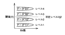
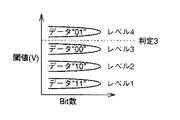
図119は、従来の2値AND型フラッシュメモリの書込みデータと、メモリセルトランジスタのしきい値との関係を示す図である。書込み動作および読出動作においては、判定レベルVj01を基準として、データの書込みおよび読出が行なわれる。
【0023】
図120は、従来の4値AND型フラッシュメモリ8000の書込みデータと、メモリセルトランジスタのしきい値との関係を示す図である。書込み動作および読出動作においては、3つの判定レベルVj1,Vj2,Vj3を基準として、データの書込みおよび読出が行なわれる。
【0024】
上述のとおり、従来の4値AND型フラッシュメモリ8000は、図119のように、2値AND型フラッシュメモリでは書込後のメモリセルトランジスタのしきい値(Vth)を“0”と“1”の2種に分割していたのに対し、図120に示すように書込み後のしきい値を4種に分割するものである。
【0025】
したがって、各々のレベルを判定するのに、3種類の判定値Vj1、Vj2、Vj3を必要とする。
【0026】
図121〜図126は、書込み動作の第1〜第3の処理ステップにおいて、データラッチDL−LおよびDL−RならびにセンスラッチSLに保持されるデータおよび書込み後のメモリセルのしきい値を示す概念図である。
【0027】
図121は、書込み動作の第1の処理ステップにおける各ラッチに保持されるデータを示し、図122は、書込み動作の第1の処理ステップにおけるメモリセルのしきい値を示す。
【0028】
図123は、書込み動作の第2の処理ステップにおける各ラッチに保持されるデータを示し、図124は、書込み動作の第2の処理ステップにおけるメモリセルのしきい値を示す。
【0029】
図125は、書込み動作の第3の処理ステップにおける各ラッチに保持されるデータを示し、図126は、書込み動作の第3の処理ステップにおけるメモリセルのしきい値を示す。
【0030】
まず、書込み動作の開始前に、メモリセルのしきい値を判定レベルVj1以下とする処理が行なわれる。
【0031】
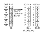
次に、図121および122を参照して、書込動作の第1ステップでは、データ入出力端子群10うちの端子I/O0〜7から入力された1バイト分のデータDQ0〜7のうち、データDQ0〜3をデータラッチDL−Rに、データDQ4〜7をデータラッチDL−Lに格納する。図121の例では、入力された1バイトのデータは、16進数表示でC9hであるものとする。
【0032】
データは、1セクタ(1ワード線に対応するデータ)すべてについて、端子I/O0〜3からの入力データDQ0〜3はデータラッチDL−Rに、端子I/O4〜7からの入力データDQ4〜7はデータラッチDL−Lにそれぞれラッチされる。
【0033】
以下では、データラッチDL−Lに保持されるデータDQ4〜7のうちの1つを上位ビットとし、データラッチDL−Rに保持されるデータDQ0〜3の1つを下位ビットとする2ビットのデータ、(DQ4、DQ0)、(DQ5、DQ1)(DQ6、DQ2)(DQ7、DQ3)をそれぞれ1組のデータとして考えることにする。
【0034】
チップコントロール部200は、まずデータラッチDL−R、DL−Lに含まれる上記のようなデータの組を演算することで、データラッチDL−Lに保持される上位ビットが“0”であって、データラッチDL−Rに保持される下位ビットが“1”となっているデータに対応するセンスラッチSLのビットデータのみを“0”レベルとする。
【0035】
図121に示すとおり、このような演算を行なった後には、センスラッチSLには、上位から“0111”というデータが保持されている。このようにしてセンスラチSLに保持されたデータに基づいて、センスラッチSLの各ビットにそれぞれ対応するメモリセルMC1〜MC4にデータの書込が行なわれる。ここで、メモリセルMC1〜MC4は、同一のワード線WLに接続している。さらに、ベリファイ動作の判定値としては第3番目の判定値Vj3を用いる。
【0036】
このとき、センスラッチ中のデータ“0”に対応するメモリセルに対してデータの書込みが行なわれる。したがって、センスラッチの最上位ビットに対応するメモリセルMC4に対してレベル4のデータ(データ“01”に対応する)の書込が行なわれる。
【0037】
実際のデータの書込は、ワード線WLに高電圧を印加することで、FN(ファウラー・ノルドハイム)トンネル電流を利用して書込まれる。
【0038】
センスラッチSLのビットデータが“1”のビットに対応するビット線BLにはワード線WLから印加される電圧を緩和するために、ワード線電圧以下の電圧が印加される。結果的に、センスラッチに保持されるビットデータが“0”に対応するビット線BLに接続するメモリセルにだけデータの書込が行なわれる。
【0039】
次に、図123および124を参照して、書込動作の第2ステップでは、データラッチDL−R、DL−Lに保持されたデータの演算を行ない、データラッチDL−Lに保持された上位ビットが“0”であり、データラッチDL−Rに保持された下位ビットが“0”であるデータの組に対応するセンスラッチSLのビットには“0”が書込まれる。ベリファイ動作における判定値をVj2に変えたうえで、データ書込においては、データDQ5およびDQ1に対応するビット線に接続するメモリセルにのみデータの書込が行なわれる。
【0040】
次に、図125および126を参照して、書込動作の第3ステップでは、データラッチDL−R、DL−Lに保持されたデータの演算を行ない、データラッチDL−Lに保持された上位ビットが“1”であり、データラッチDL−Rに保持された下位ビットが“0”であるデータの組に対応するセンスラッチSLのビットには“0”が書込まれる。ベリファイ動作における判定値をVj1に変えたうえで、データ書込においては、データDQ6およびDQ2に対応するビット線に接続するメモリセルにのみデータの書込が行なわれる。
【0041】
以上のようにして、書込むデータをすべて入力後、3回の演算と書込処理を経て書込動作が終了する。
【0042】
[従来の4値データの読出動作]
次に、読出動作について説明する。
【0043】
図127〜図132は、読出動作の第1〜第3の処理ステップにおいて、データラッチDL−LおよびDL−RならびにセンスラッチSLに保持されるデータおよび読出時のメモリセルのしきい値と判定レベルを示す概念図である。
【0044】
図127は、読出動作の第1の処理ステップにおける各ラッチに保持されるデータを示し、図128は、読出動作の第1の処理ステップにおけるメモリセルのしきい値と判定レベルを示す。
【0045】
図129は、読出動作の第2の処理ステップにおける各ラッチに保持されるデータを示し、図130は、読出動作の第2の処理ステップにおけるメモリセルのしきい値と判定レベルを示す。
【0046】
図131は、読出動作の第3の処理ステップにおける各ラッチに保持されるデータを示し、図132は、読出動作の第3の処理ステップにおけるメモリセルのしきい値と判定レベルを示す。
【0047】
まず、図127および128を参照して、読出動作の第1の処理ステップにおいては、第1の判定レベルVj1で読出を行ない、結果をセンスラッチSLに格納する。そのデータをデータラッチDL−Rに転送し、センスラッチSLをクリアする。
【0048】
次に、図129および130を参照して、読出動作の第2の処理ステップにおいては、第2の判定レベルVj2で読出を行ない、結果をセンスラッチSLに格納する。そのデータをデータラッチDL−Lに転送し、再びセンスラッチSLをクリアする。
【0049】
最後に、図131および132を参照して、読出動作の第3の処理ステップにおいては、第3の判定レベルVj3でデータの読出を行ない、読出結果をセンスラチSLに格納する。チップコントロール回路200は、そのセンスラチSLに格納されたデータとデータラッチDL−Rのデータがともに“0”であるビット位置においてのみ、データラッチDL−Rのデータを“1”にする。
【0050】
データラッチDL−LからDQ4〜7、データラッチDL−RからDQ0〜3が順次出力される。
【0051】
このように読出動作においても、3回の読出動作のすべてが確定してからデータ出力が行なわれている。
【0052】
多値メモリのより詳しい構成については、たとえば、特開平9−297996号公報等にもその一例が開示されている。ただし、読出および書込み動作において、複数回の処理ステップの動作を行なうことが必要となる点は、以上説明した多値メモリの構成と同様である。
【0053】
【発明が解決しようとする課題】
以上説明したとおり、従来のAND型4値フラッシュメモリ8000では、書込、読出とも通常の2値フラッシュメモリに比べて、複数回の処理ステップの動作を行なうことによる遅延が、チップの読出および書込動作の速度を劣化させている。また、さらに多値化が進むほど、この速度の劣化は深刻になる。
【0054】
この発明は、上記のような問題点を解決するためになされたもので、その目的は、1メモリセルに多値データを保持させる場合でも、速度の劣化を抑えることが可能な不揮発性半導体記憶装置を提供することである。
【0055】
【課題を解決するための手段】
この発明に係る不揮発性半導体記憶装置は、複数のメモリセルが配置されたメモリセルアレイを備える。各メモリセルは、しきい電圧が第1〜第4のしきい値レベルのうちのいずれかのしきい値レベルに選択的に設定されて、互いに異なる4つのデータコードのうちのいずれかのデータコードを記憶し、各データコードは第1および第2のデータを含む。第1のしきい値レベルは第1の判定レベルよりも低く、第2のしきい値レベルは第1の判定レベルよりも高く第2の判定レベルよりも低く、第3のしきい値レベルは第2の判定レベルよりも高く第3の判定レベルよりも低く、第4のしきい値レベルは第3の判定レベルよりも高い。第1〜第4のしきい値レベルは、4つのデータコードを、i)第1のステップでは、各データコードの第1のデータが第1および第2の論理のうちのいずれの論理であるかに応じて2つのグループに分けて並べ替え、ii)第2のステップでは、各グループの2つのデータコードを、さらに、各データコードの第2のデータが第1および第2の論理のうちのいずれの論理であるかに応じて並べ替える、という手順に相当する手続きで並べ替えたものとそれぞれ対応する。第1および第2のしきい値レベルに対応する各データコードの第1のデータは第1の論理であり、第3および第4のしきい値レベルに対応する各データコードの第1のデータは第2の論理である。データコードの第1のデータが第1の論理であるグループにおいては、第2のデータが第1の論理であるデータコードの方が第2のデータが第2の論理であるデータコードよりも低いしきい値レベルに対応する。データコードの第1のデータが第2の論理であるグループにおいては、第2のデータが第1の論理であるデータコードの方が第2のデータが第2の論理であるデータコードよりも高いしきい値レベルに対応する。この不揮発性半導体記憶装置は、アドレス信号に応じて、メモリセルアレイの複数のメモリセルのうちのいずれかm個(ただし、mは2以上の整数である)のメモリセルを一括して選択するセル選択回路と、第1〜第3の判定レベルに基づいて、セル選択回路によって選択されたm個のメモリセルに対してm個のデータコードの読出/書込動作を行なうデータ読出/書込回路と、不揮発性半導体装置の外部とデータ読出/書込回路との間で、m個のデータコードの第1および第2のデータをkビット(ただし、kは自然数である)ごとにk個の入出力ノードを介して授受するデータ入出力回路とをさらに備える。各データコードの第1および第2のデータは、それぞれ異なるタイミングで同一の入出力ノードを介して授受される。また、データ読出/書込回路は、m個のメモリセルのしきい値電圧と第2の判定レベルとを比較する第1の読出ステップと、m個のメモリセルのしきい値電圧と第1の判定レベルとを比較する第2の読出ステップと、m個のメモリセルのしきい値電圧と第3の判定レベルとを比較する第3の読出ステップとを実行し、第1の読出ステップの比較結果であるm個のデータコードの第1のデータを保持する第1の読出データ保持回路と、第2の読出ステップの比較結果であるmビットの第1の判定データを保持する第2の読出データ保持回路と、第3の読出ステップの比較結果であるmビットの第2の判定データを保持する第3の読出データ保持回路と、第2の読出データ保持回路に保持されたmビットの第1の判定データと第3の読出データ保持回路に保持されたmビットの第2の判定データとに基づいてm個のデータコードの第2のデータを生成する読出データ変換回路とを含む。また、データ読出/書込回路は、第1の読出ステップの後に第2および第3の読出ステップを実行し、第1の読出データ保持回路に保持されたmビットの第1のデータがデータ入出力回路によって外部に出力されている期間中に、第2または第3の読出ステップを実行する。
また、この発明に係る他の不揮発性半導体記憶装置では、データ読出/書込回路は、第2および第3の読出ステップの後に第1の読出ステップを実行し、読出データ変換回路によって生成されたmビットの第2のデータがデータ入出力回路によって外部に出力されている期間中に、第1の読出ステップを実行する。
【0056】
また、この発明に係るさらに他の不揮発性半導体記憶装置は、複数のメモリセルが配置されたメモリセルアレイを備える。各メモリセルは、しきい電圧が第1〜第4のしきい値レベルのうちのいずれかのしきい値レベルに選択的に設定されて、互いに異なる4つのデータコードのうちのいずれかのデータコードを記憶し、各データコードは第1および第2のデータを含む。第1のしきい値レベルは第1の判定レベルよりも低く、第2のしきい値レベルは第1の判定レベルよりも高く第2の判定レベルよりも低く、第3のしきい値レベルは第2の判定レベルよりも高く第3の判定レベルよりも低く、第4のしきい値レベルは第3の判定レベルよりも高い。第1〜第4のしきい値レベルは、4つのデータコードを、i)第1のステップでは、各データコードの第1のデータが第1および第2の論理のうちのいずれの論理であるかに応じて2つのグループに分けて並べ替え、ii)第2のステップでは、各グループの2つのデータコードを、さらに、各データコードの第2のデータが第1および第2の論理のうちのいずれの論理であるかに応じて並べ替える、という手順に相当する手続きで並べ替えたものとそれぞれ対応する。第1および第2のしきい値レベルに対応する各データコードの第1のデータは第1の論理であり、第3および第4のしきい値レベルに対応する各データコードの第1のデータは第2の論理である。データコードの第1のデータが第1の論理であるグループにおいては、第2のデータが第1の論理であるデータコードの方が第2のデータが第2の論理であるデータコードよりも低いしきい値レベルに対応する。データコードの第1のデータが第2の論理であるグループにおいては、第2のデータが第1の論理であるデータコードの方が第2のデータが第2の論理であるデータコードよりも高いしきい値レベルに対応する。不揮発性半導体記憶装置はさらに、アドレス信号に応じて、メモリセルアレイの複数のメモリセルのうちのいずれかm個(ただし、mは2以上の整数である)のメモリセルを一括して選択するセル選択回路と、第1〜第3の判定レベルに基づいて、セル選択回路によって選択されたm個のメモリセルからm個のデータコードを読み出すデータ読出回路と、データ読出回路によって読み出されたm個のデータコードの第1および第2のデータを、kビット(ただし、kは自然数である)ごとにk個の出力ノードを介して不揮発性半導体記憶装置の外部に出力するデータ出力回路とを備える。各データコードの第1および第2のデータは、それぞれ異なるタイミングで同一の出力ノードを介して出力される。また、データ読出回路は、m個のメモリセルのしきい値電圧と第2の判定レベルとを比較する第1の読出ステップと、m個のメモリセルのしきい値電圧と第1の判定レベルとを比較する第2の読出ステップと、m個のメモリセルのしきい値電圧と第3の判定レベルとを比較する第3の読出ステップとを実行し、第1の読出ステップの比較結果であるm個のデータコードの第1のデータを保持する第1の読出データ保持回路と、第2の読出ステップの比較結果であるmビットの第1の判定データを保持する第2の読出データ保持回路と、第3の読出ステップの比較結果であるmビットの第2の判定データを保持する第3の読出データ保持回路と、第2の読出データ保持回路に保持されたmビットの第1の判定データと第3の読出データ保持回路に保持されたmビットの第2の判定データとに基づいてm個のデータコードの第2のデータを生成する読出データ変換回路とを含む。また、データ読出回路は、第1の読出ステップの後に第2および第3の読出ステップを実行し、第1の読出データ保持回路に保持されたmビットの第1のデータがデータ出力回路によって外部に出力されている期間中に、第2または第3の読出ステップを実行する。
また、この発明に係るさらに他の不揮発性半導体記憶装置では、データ読出回路は、第2および第3の読出ステップの後に第1の読出ステップを実行し、読出データ変換回路によって生成されたmビットの第2のデータがデータ出力回路によって外部に出力されている期間中に、第1の読出ステップを実行する。
【0067】
【発明の実施の形態】
[実施の形態1]
図1は、本発明の実施の形態1の不揮発性半導体記憶装置であるフラッシュメモリ1000の構成を示す概略ブロック図である。
【0068】
メモリセルアレイ100は、フローティングゲートとコントロールゲートを備えた多数のメモリセルを有する。図1においても、メモリセルアレイ100は、2つのメモリセルブロック100Rと100Lとに分割されている。
【0069】
メモリセルのコントロールゲートはワード線WLに、メモリセルのドレインはビット線BLに、メモリセルのソースは図示しないソース線SCLに接続される。
【0070】
ワード線WLおよびビット線BLは代表的に、それぞれ2本ずつ示されている。
【0071】
ロウデコーダ110は、外部からアドレス信号入力端子群12およびアドレスバッファ146を介して与えられるアドレス信号A0−Akに基づいてワード線を選択的に駆動する。ビット線BLの一端側には、センスラッチ回路120が設けられる。また、ビット線BLはカラムデコーダ130からアドレス信号A0−Akに応じて出力される選択信号に基づいて選択され、選択されたビット線との間で読出データ、書込みデータの授受が行なわれる。
【0072】
図1において、図示しないが、センスラッチ回路120は、カラムデコーダ130からの選択信号に基づいて、ビット線を選択するためのカラムスイッチ回路を含んでいる。
【0073】
チップコントロール部200は、制御信号入力端子群14からコマンドバッファ回路144を介して与えられるアクセス制御信号やクロック信号を外部から受け、これに従ってメモリセルの書込制御や読出制御のために、フラッシュメモリの内部回路を全体的に制御する制御回路210を含む。消去、書込、読出などの動作モードに応じて、ワード線の電位を駆動するワードドライバ(図示せず)等の動作電圧の切換は、制御回路210が電源発生部150を制御することにより行なわれる。
【0074】
データラッチ回路DL−LおよびDL−Rは、データの書込み、読出動作において授受されるデータを一時保持するデータバッファである。
【0075】
チップコントロール部200は、さらに、後に説明するように、制御回路210に制御されて、読出し動作においてデータラッチ回路DL−LおよびDL−Rならびにセンスラッチ回路120に保持されたデータを演算して、読出しデータを生成する読出しデータ変換回路220と、制御回路210に制御されて、書込み動作においてデータラッチ回路DL−LおよびDL−Rならびにセンスラッチ回路120に保持されたデータを演算して、書込みデータを生成する書込みデータ変換回路230とを含む。
【0076】
フラッシュメモリ1000の動作モードは、特に制限されないが、外部からチップコントロール部200に供給されるアクセス制御信号、またはデータバスなどを介して供給されるコマンドデータによって指示され、データの書換(消去および書込)やデータの読出モードを有する。
【0077】
図1に示されるAND型4値フラッシュメモリ1000においても、1つのメモリセルの情報記憶状態は、消去状態、第1の書込状態、第2の書込状態、第3の書込状態の中から選ばれた1つの状態とされている。
【0078】
そのために、フラッシュメモリ1000も、書込動作時にワード線に印加する書込ベリファイ電圧を相互に異なる3種類設定し、これらを順次切換えて、3回に分けて書込処理を行なう。ただし、後に説明するように、上記4つの情報記憶状態に対応する2ビットデータの配列と、これら3回の書込処理の順序とを工夫することにより、書込み時間および読出し時間の短縮を可能とする。
【0079】
これら各書込動作において、制御回路210は、書込みデータ変換回路230を制御して、データラッチDL−LおよびDL−Rに保持された書込みデータに基づいて、各書込み動作において、センスラッチSL(センスラッチ回路120に含まれるセンスラッチSL)に保持させるべき2値(1ビット)のラッチデータ“0”または“1”(“L”または“H”)の演算を行わせる。制御回路210は、上記3回に分けた書込動作の各書込動作ごとに、対応する書込ベリファイ電圧を設定して書込み動作を制御する。
【0080】
ここで、従来のフラッシュメモリ8000の構成では、データラッチ回路DL−LおよびDL−Rにそれぞれ保持されるのは、同一のタイミングでデータ入出力端子群10に与えられたデータ列を分割した2つのデータ列であった。
【0081】
これに対して、本願のフラッシュメモリ1000では、従来のフラッシュメモリ8000の構成と異なり、データラッチ回路DL−LおよびDL−Rにそれぞれ保持されるのは、後に説明するように、異なったタイミングでデータ入出力端子群10に与えられ、同一のワード線に結合する同一のメモリセル群に与えられる2組のデータ列、または同一のワード線に結合するが異なったビット線と結合するメモリセル群に与えられる2組のデータ列である。このような構成により、1つのメモリセルに4値(2ビット)の情報を書込むことが可能となる。
【0082】
また、フラッシュメモリ1000も、読出動作時にワード線の印加するワード線選択レベルとして電圧を3種類設定し、3回の読出動作でメモリセルから読出される2値(1ビット)のデータをセンスラッチ回路120を介してデータラッチ回路DL−LおよびDL−Rに取り込む。3回の読出動作中に順次、読出しデータ変換回路220は、これらラッチ回路に保持されたデータを4値(2ビット)の情報に変換し、制御回路210はデータ入出力端子群10から出力させる。
【0083】
以下、上に述べた書込動作、読出動作について、さらに詳細を説明する。
[4値データの読出動作]
実施の形態1におけるフラッシュメモリ1000では、上述のとおり、入出力データのデータラッチDL―LおよびDL−Rの格納方法が従来のフラッシュメモリ8000とは異なる。
【0084】
1つのメモリセルに格納されるデータは、従来の多値フラッシュメモリ8000では、同じタイミングでデータ入出力端子群10から入力された1バイトのデータのうち、データDQ0とDQ4、データDQ1とDQ5のように、同一バイト内のデータで構成されている。本発明の4値フラッシュメモリ1000では、1つのメモリセルに格納されるデータは、従来の2値フラッシュメモリと異なり、異なるワード線の同じYアドレスであって、かつ同じI/Oのビットに対応していたデータか、あるいは同一セクタ(同一ワード線)のYアドレスがどこか異なっていた同一I/Oのデータ(同一セクタの異なるYアドレスの同一I/Oに対応するデータ)に相当するデータである。
【0085】
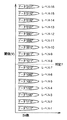
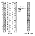
図2〜7は、本発明の実施の形態1の動作説明図であり、読出動作の第1〜第3の処理ステップにおいて、データラッチDL−LおよびDL−RならびにセンスラッチSLに保持されるデータおよび読出時のメモリセルのしきい値と判定レベルを示す概念図である。
【0086】
図2は、読出動作の第1の処理ステップにおける各ラッチに保持されるデータを示し、図3は、読出動作の第1の処理ステップにおけるメモリセルのしきい値と判定レベルを示す。
【0087】
図4は、読出動作の第2の処理ステップにおける各ラッチに保持されるデータを示し、図5は、読出動作の第2の処理ステップにおけるメモリセルのしきい値と判定レベルを示す。
【0088】
図6は、読出動作の第3の処理ステップにおける各ラッチに保持されるデータを示し、図7は、読出動作の第3の処理ステップにおけるメモリセルのしきい値と判定レベルを示す。
【0089】
まず、図2および図3を参照して、読出動作の第1の処理ステップにおいては、同一のワード線に接続された複数メモリセル、たとえば、1kByte分のメモリセルから、第2の判定レベルVj2で一括して読出を行ない、その結果をセンスラッチ回路120に格納する。
【0090】
図2では、センスラッチ回路120中において、1セクタ分の読出動作で、最初にデータ入出力端子群10から出力される1バイト分のデータを保持するセンスラッチSLと、これに対応するデータラッチDL−LおよびDL−Rを抜き出して示す。1セクタ分の読出動作で、この1バイト分のデータに続いてデータ入出力端子群10から読み出されるデータについても、以下に説明するのと同様の処理が並行して行なわれている。
【0091】
このデータ入出力端子群10から最初に出力される1バイト分のデータを含むデータ列を保持するメモリセル列MC0〜MC7には、それぞれデータ“11”,“01”,“00”,“10”,“01”,“00”,“10”,“11”が保持されているものとする。したがって、図2において、センスラッチ回路120の1バイト分の領域に保持されるデータは、16進数表示で、C9hである。
【0092】
第2の判定レベルVj2で一括して読出されたデータは、センスラッチSLからデータラッチDL−Lに格納される。この時点で、制御回路210の制御により、データラッチDL−Lに格納されたデータが、順次1バイトずつデータ入出力端子群10から出力される。この時点でデータラッチ回路DL−Lに格納されているデータは、従来の2値フラッシュメモリの読出動作における1セクタ分のデータの半分に相当する。
【0093】
このように、読出動作の第1の処理ステップにおいて、第2の判定レベルVj2で読出動作をまず行なうのは、図3に示すとおり、このレベルで読出すことにより、メモリセル内の4種のデータが、“0”または“1”のうちのいずれであるかが確定するからである。すなわち、メモリセルMC0〜MC7に格納されるデータの上位のビットの0または1が確定することになる。
【0094】
次に、図4および図5を参照して、読出動作の第2の処理ステップにおいては、第1の処理ステップでセンスラッチSLからデータラッチDL−Lにデータを格納し、センスラッチSLがクリアされた時点で、第1の判定レベルVj1で読出動作を行ない、読み出されたデータをセンスラッチ回路120に格納する。つまり、データラッチ回路DL−Lからはデータ出力を行なっている途中で、センスラッチSLからデータラッチDL−Rにデータ転送を行なう。データラッチDL−Rへのデータ転送後、センスラッチ回路120はクリアされる。
【0095】
次に、図6および図7を参照して、読出動作の第3の処理ステップにおいては、第3の判定レベルVj3で読出動作を行ない、センスラッチ回路120にデータを格納する。読出データ変換回路220は、センスラッチSLに保持されるデータとデータラッチDL−Rに保持されるデータとの間で演算を行ない、ともに“0”のビットデータのところだけ、データラッチDL−Rのビットデータを“1”に変更する。
【0096】
データラッチDL−Lのデータ出力が終了した後、制御回路210は、データラッチDL−Rからデータ入出力端子群10へデータ出力を開始する。
【0097】
従来の4値フラッシュメモリ8000では、セクタサイズは、たとえば、2KByteであって、1Byte当り50nsで出力動作を行なっている。したがって、セクタの半分である1KByteを出力するのに50μsだけの時間が必要となっている。
【0098】
また、従来の4値フラッシュメモリ8000でも、つまり3回読出動作を行なった後にはじめてデータ出力を開始する場合でも、出力直前までの時間(ファーストアクセス時間と呼ぶ)は50μsで完了するため、本願発明の4値フラッシュメモリ1000において、1/2セクタ分のデータを出力している間に、上記第1の判定レベルから第3の判定レベルまでのアクセス動作を完了させることは可能である。
【0099】
したがって、4値フラッシュメモリ1000では、読出コマンドの入力後、データが出力されるようになるまでには、第2の判定レベルVj2の判定結果が出るまでの時間だけ経過すればよい。これは、2値の読出時間と同等であるため、メモリセルに記憶されるデータが4値化されたことによる速度の劣化が生じないことを意味する。
【0100】
もしも、出力速度が非常に速く(またはファーストアクセス時間が非常に長く)データラッチDL−Rのデータが確定する前に、データラッチDL−Lの出力が終了する場合には、データラッチDL−LとデータラッチDL−Rからのデータ出力の間に待ち時間が生じることになる。しかしながら、この場合でも、データ値DL−Lの出力時間分だけ従来のデータ読出動作よりも読出速度が改善されることになる。
【0101】
ただし、通常は、このような待ち時間が生じないようにセクタサイズを調整する。つまり、読出時間(ファーストアクセス時間)でセクタサイズ(1ワード線に接続されるメモリセルから出力されるデータ量)を決めればよいことになる。
【0102】
このような条件を満たすためには、セクタサイズは以下の式を満足する必要がある。
{セクタサイズ(Byte)×(1Byte当りの出力時間)×1/2}≧{1回の読出時間×2} …(1)
図8は、実施の形態1のフラッシュメモリ1000の読出動作を説明するためのタイミングチャートである。
【0103】
図8を参照して、時刻t1において、まず、第2の判定レベルVj2での読出動作が行なわれ、センスラッチ回路120に格納される。
【0104】
続いて、時刻t2において、センスラッチ回路120に保持されたデータは、データラッチDL−Lに転送され、センスラッチ回路120はクリアされる。
【0105】
時刻t3において、第1の判定レベルVj1に基づく読出動作が開始される。
一方、時刻t4において、制御回路210の制御により、データラッチDL−Lに保持されている1/2セクタ分のデータの出力が開始される。
【0106】
時刻t5において、第1の判定レベルVj1に基づいて読み出され、センスラッチ回路120に保持されているデータが、データラッチDL−Rに格納される。一方、センスラッチ回路120は、クリアされる。
【0107】
時刻t6において、第3の判定レベルVj3に基づく読出動作が開始され、センスラッチ回路120に読出データが格納される。
【0108】
第3の判定レベルVj3に基づく読出動作の完了後、時刻t7において、制御回路210により制御されて、読出データ変換回路220は、センスラッチ回路120に保持されたデータと、データラッチ回路DL−Rに保持されたデータとの間で演算を行ない、ともに“0”のビットデータのところだけ、データラッチDL−Rに保持されるビットデータを“1”に変更する。
【0109】
時刻t9において、データラッチ回路DL−Rに保持されている残り1/2セクタ分のデータの出力が開始される。時刻t10において、1セクタ分のデータ出力が完了する。
【0110】
以上説明したとおり、時刻t1において読み出されたデータ列の出力が行なわれている期間中に、このデータ列に続いて出力されるべきデータ列の読出動作が完了しているために、4値メモリセルからの読出データを出力する際の遅延時間を削減することが可能である。
【0111】
[実施の形態1の変形例1]
実施の形態1では、図2および3で示される処理を行なった後、データラッチDL−Lに保持されたデータを出力中に、図4および5で示される処理と、図6および7で示される処理を行なう構成であった。しかしながら、本願発明は、必ずしも、このような処理の順番に制限されるわけではなく、たとえば、図4および5で示される処理と、図6および7で示される処理を行なった後に、言いかえると、第1の判定レベルVj1で読出を行ない、読出結果をデータラッチDL−Rに格納し、続いて、第3の判定レベルVj3で読出を行ない、センスラッチSLに格納されたデータと、データラッチDL−Rに格納されたデータとの間で演算を行なった後にデータラッチDL−Rからのデータ出力を行なっている間に、図2および3で示される処理を行なう構成としてもよい。この場合、データラッチDL−Rからのデータ出力が終了後に、第2の判定レベルで読み出され、データデータラッチDL−Lに格納されているデータの出力が開始されることになる。
【0112】
実施の形態1に比べて、読出動作時間の短縮効果は小さいものの、従来の4値フラッシュメモリ8000よりも、短い時間でデータ読出を行なうことが可能である。
【0113】
もちろん、上記のように第1〜第3の読出処理を連続して行なう必要も必ずしもなく、メモリセルMC0〜MC7に保持されているデータを、上位ビット、または下位ビットの1ビットずつ読み出す構成とすることも可能である。
【0114】
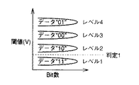
[実施の形態1の変形例2]
上述のとおり、実施の形態1では、読出動作の第1の処理ステップにおいては、第2の判定レベルVj2で読出動作をまず行なうことにより、メモリセル内の4種のデータが、“0”または“1”のうちのいずれであるかが確定するように、書込みレベルと書込みデータを対応付けていた。
【0115】
図9〜図12は、逆に、このように1回の読出処理では、上位ビットおよび下位ビットのいずれも確定できないような書込みレベルと書込みデータを対応付けの例をそれぞれ示す。また、これら、図9〜図12のそれぞれの場合において、“0”と“1”とを置換したデータの配列としたときも、1回の読出処理では、上位ビットおよび下位ビットのいずれも確定できない。
【0116】
これに対して、実施の形態1の変形例2の読出動作では、実施の形態1と同様に読出時間の削減が可能な書込みデータと書込みレベルの別の対応関係の例を与える。
【0117】
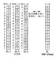
図13は、実施の形態1の変形例2の読出動作の第2の処理ステップにおける各ラッチに保持されるデータを示し、図14は、実施の形態1の変形例2の読出動作の第2の処理ステップにおけるメモリセルのしきい値と判定レベルを示す。
【0118】
つまり、図14に示すように、図3に示したデータ配置において、データ“00”とデータ“01”とを入れ換えたデータ配置においても、実施の形態1と同様の処理で、読出時間を短縮することが可能である。
【0119】
この場合、まず、読出動作の第1の処理ステップにおいては、同一のワード線に接続された複数メモリセルから、第2の判定レベルVj2で一括して読出を行ない、その結果をセンスラッチ回路120に格納する。
【0120】
このデータ入出力端子群10から最初に出力される1バイト分のデータを含むデータ列を保持するメモリセル列MC0〜MC7には、それぞれデータ“11”,“00”,“01”,“10”,“00”,“01”,“10”,“11”が保持されているものとする。したがって、データラッチ回路DL−Lの1バイト分の領域に保持されるデータは、16進数表示で、C9hである。
【0121】
第2の判定レベルVj2で一括して読出されたデータは、センスラッチSLからデータラッチDL−LおよびDL−Rの双方に格納される。この時点で、制御回路210の制御により、データラッチDL−Lに格納されたデータが、順次1バイトずつデータ入出力端子群10から出力される。この時点でデータラッチ回路DL−LおよびDL−Rに格納されているデータは、従来の2値フラッシュメモリの読出動作における1セクタ分のデータの半分に相当する。
【0122】
このように、実施の形態1の変形例2の読出動作の第1の処理ステップにおいても、第2の判定レベルVj2で読出動作をまず行なうことにより、メモリセル内の4種のデータの上位ビットが、“0”または“1”のうちのいずれであるかが確定する。
【0123】
次に、図13および図14を参照して、読出動作の第2の処理ステップにおいては、第1の処理ステップでセンスラッチSLからデータラッチDL−LおよびDL−Rにデータを格納し、センスラッチSLがクリアされた時点で、第1の判定レベルVj1で読出動作を行ない、読み出されたデータをセンスラッチ回路120に格納する。データラッチDL−Lからのデータ出力が行なわれている間に、読出データ変換回路220は、センスラッチSLに保持されるデータとデータラッチDL−Rに保持されるデータとの間で演算を行ない、センスラッチSLのビットデータが“0”であり、かつ、データラッチDL−Rの対応するビットデータが“1”となっている場合は、データラッチDL−Rの上記対応するビットデータを“0”とし、それ以外の場合は、データラッチDL−Rのビットデータを“1”に変更する。データラッチDL−Rのデータ変更後、センスラッチ回路120はクリアされる。
【0124】
次に、読出動作の第3の処理ステップにおいては、第3の判定レベルVj3で読出動作を行ない、センスラッチ回路120にデータを格納する。読出データ変換回路220は、センスラッチSLに保持されるデータとデータラッチDL−Rに保持されるデータとの間で演算を行ない、ともに“0”のビットデータのところだけ、データラッチDL−Rのビットデータを“1”に変更する。
【0125】
データラッチDL−Lのデータ出力が終了した後、制御回路210は、データラッチDL−Rからデータ入出力端子群10へデータ出力を開始する。
【0126】
図15は、実施の形態1の変形例2のフラッシュメモリの読出動作を説明するためのタイミングチャートである。
【0127】
図15を参照して、時刻t1において、まず、第2の判定レベルVj2での読出動作が行なわれ、センスラッチ回路120に格納される。
【0128】
続いて、時刻t2において、センスラッチ回路120に保持されたデータは、データラッチDL−LおよびDL−Rに転送され、センスラッチ回路120はクリアされる。
【0129】
時刻t3において、第1の判定レベルVj1に基づく読出動作が開始される。一方、時刻t4において、制御回路210の制御により、データラッチDL−Lに保持されている1/2セクタ分のデータの出力が開始される。
【0130】
時刻t5において、読出データ変換回路220は、センスラッチSLに保持されるデータとデータラッチDL−Rに保持されるデータとの間で演算を開始し、時刻t6から、センスラッチSLのビットデータが“0”であり、かつ、データラッチDL−Rの対応するビットデータが“1”となっている場合は、データラッチDL−Rの上記対応するビットデータを“0”とし、それ以外の場合は、データラッチDL−Rのビットデータを“1”に変更する。
【0131】
時刻t7において、センスラッチ回路120は、クリアされる。
時刻t8において、第3の判定レベルVj3に基づく読出動作が開始され、センスラッチ回路120に読出データが格納される。
【0132】
第3の判定レベルVj3に基づく読出動作の完了後、時刻t9において、制御回路210により制御されて、読出データ変換回路220は、センスラッチ回路120に保持されたデータと、データラッチ回路DL−Rに保持されたデータとの間で演算を開始し、時刻t10から、ともに“0”のビットデータのところだけ、データラッチDL−Rに保持されるビットデータを“1”に変更する。
【0133】
時刻t11において、データラッチ回路DL−Rに保持されている残り1/2セクタ分のデータの出力が開始される。
【0134】
時刻t12において、1セクタ分のデータ出力が完了する。
以上の読出動作によっても、実施の形態1の読出動作と同様の効果が奏される。
【0135】
[実施の形態2]
図16は、実施の形態2のフラッシュメモリのセンスラッチ回路120とビット線との接続の切り換え方式の概念を示す図であり、図16(a)は、センスラッチ回路120中において1ビットのデータに対応するセンスラッチSLに対して、ビット線BL1が接続されている場合を示し、図16(b)は、上記センスラッチSLに対して、ビット線BL2が接続されている場合を示す。
【0136】
実施の形態2のフラッシュメモリの構成は、図16に示す構成と制御回路210の制御動作以外は、基本的に実施の形態1のフラッシュメモリ1000の構成と同様である。
【0137】
図16に示すような構成とすることで、1つのワード線WLが選択されている状態で、ビット線からのセンスラッチ回路120へのデータの取りこみが、隣接するメモリセル列について分割して行なわれる場合、各メモリセル列からのデータの読出ごとに、第1〜第3の処理ステップを分割して並行に処理することが可能となり、以下に説明するように、さらに高速化を図ることが可能となる。
【0138】
図17は、図16において示した概念を具体的に実現するための回路構成を示す図である。図17では、センスラッチ回路120中の各ビットデータに対応するセンスラッチのうち2つに関する構成を代表として抜き出して示す。
【0139】
図17を参照して、たとえば、1つのワード線WLnに接続するゲートを有するメモリセルトランジスタMC1nm、MC2nm、MC1nm+1、MC2nm+1のドレインは、それぞれサブビット線SBL1m、SBL2m、SBL1m+1、SBL2m+1に接続されている。メモリセルトランジスタは、コントロールゲートとフローティングゲートを有する、いわゆるフローティングゲートトランジスタである。
【0140】
サブビット線SBL1m、SBL2mは、それぞれ、トランジスタTr1m,Tr2mを介してメインビット線MBLmに接続している。トランジスタTr1mのゲートは信号BSS1により制御され、トランジスタTr2mのゲートは信号BSS2により制御される。
【0141】
サブビット線SBL1m+1、SBL2m+1は、それぞれ、トランジスタTr1m+1,Tr2m+1を介してメインビット線MBLm+1に接続している。トランジスタTr1m+1のゲートは信号BSS1により制御され、トランジスタTr2m+1のゲートは信号BSS2により制御される。
【0142】
メインビット線MBLmは、ゲート電位が信号STGにより制御されるゲートトランジスタTGmを介して、センスラッチ回路120中の1ビットデータに対応するラッチ回路SLmと接続する。メインビット線MBLm+1は、ゲート電位が信号STGにより制御されるゲートトランジスタTGm+1を介して、センスラッチ回路120中の他の1ビットデータに対応するラッチ回路SLm+1と接続する。
【0143】
なお、1つのメインビット線に接続されるサブビット線の本数は、図17のように2本に限定されるわけではなく、さらに多くてもよい。
【0144】
図18〜29は、本発明の実施の形態2の動作説明図であり、読出動作の第1〜第6の処理ステップにおいて、データラッチDL−LおよびDL−RならびにセンスラッチSLに保持されるデータおよび読出時のメモリセルのしきい値と判定レベルを示す概念図である。
【0145】
図18は、読出動作の第1の処理ステップにおける各ラッチに保持されるデータを示し、図19は、読出動作の第1の処理ステップにおけるメモリセルのしきい値と判定レベルを示す。
【0146】
図20は、読出動作の第2の処理ステップにおける各ラッチに保持されるデータを示し、図21は、読出動作の第2の処理ステップにおけるメモリセルのしきい値と判定レベルを示す。
【0147】
図22は、読出動作の第3の処理ステップにおける各ラッチに保持されるデータを示し、図23は、読出動作の第3の処理ステップにおけるメモリセルのしきい値と判定レベルを示す。
【0148】
図24は、読出動作の第4の処理ステップにおける各ラッチに保持されるデータを示し、図25は、読出動作の第4の処理ステップにおけるメモリセルのしきい値と判定レベルを示す。
【0149】
図26は、読出動作の第5の処理ステップにおける各ラッチに保持されるデータを示し、図27は、読出動作の第5の処理ステップにおけるメモリセルのしきい値と判定レベルを示す。
【0150】
図28は、読出動作の第6の処理ステップにおける各ラッチに保持されるデータを示し、図29は、読出動作の第6の処理ステップにおけるメモリセルのしきい値と判定レベルを示す。
【0151】
まず、図18および図19を参照して、読出動作の第1の処理ステップにおいては、同一のワード線に接続された複数メモリセル、たとえば、1kByte分のメモリセルから、第2の判定レベルVj2で一括して読出を行ない、その結果をセンスラッチ回路120に格納する。
【0152】
図18では、センスラッチ回路120中において、1セクタ分の読出動作で、最初にデータ入出力端子群10から出力される1バイト分のデータを保持するセンスラッチSLと、これに対応するデータラッチDL−LおよびDL−Rを抜き出して示す。1セクタ分の読出動作で、この1バイト分のデータに続いてデータ入出力端子群10から読み出されるデータについても、以下に説明するのと同様の処理が並行して行なわれている。
【0153】
図17のサブビット線のうち信号BSS1により選択されるサブビット線SBL1m、SBL1m+1等に接続し、かつ、データ入出力端子群10から最初に出力される1バイト分のデータを含むデータ列を保持するメモリセル列MC1n0〜MC1n7には、それぞれデータ“11”,“01”,“00”,“10”,“01”,“00”,“10”,“11”が保持されているものとする。したがって、図18において、センスラッチ回路120の1バイト分の領域に保持されるデータは、16進数表示で、C9hである。
【0154】
第2の判定レベルVj2で一括して読出されたデータは、センスラッチSLからデータラッチDL−Lに格納される。この時点で、制御回路210の制御により、データラッチDL−Lに格納されたデータが、順次1バイトずつデータ入出力端子群10から出力される。この時点でデータラッチ回路DL−Lに格納されているデータは、従来の2値フラッシュメモリの読出動作における1セクタ分のデータの1/4に相当する。
【0155】
このように、読出動作の第1の処理ステップにおいて、第2の判定レベルVj2で読出動作をまず行なうのも、図19に示すとおり、このレベルで読出すことにより、メモリセル内の4種のデータが、“0”または“1”のうちのいずれであるかが確定するからである。すなわち、メモリセルMC1n0〜MC1n7に格納されるデータの上位のビットの0または1が確定することになる。
【0156】
次に、図20および図21を参照して、読出動作の第2の処理ステップにおいては、第1の処理ステップでセンスラッチSLからデータラッチDL−Lにデータを格納し、センスラッチSLがクリアされた時点で、第2の判定レベルVj2で、図17のサブビット線のうち信号BSS2により選択されるサブビット線SBL2m、SBL2m+1等に接続するメモリセル列MC2n0〜MC2n7から読出動作を行ない、読み出されたデータをセンスラッチ回路120に格納する。
【0157】
メモリセル列MC2n0〜MC2n7にも、それぞれデータ“11”,“01”,“00”,“10”,“01”,“00”,“10”,“11”が保持されているものとする。したがって、図20において、センスラッチ回路120の1バイト分の領域に保持されるデータも、16進数表示で、C9hである。
【0158】
つまり、データラッチ回路DL−Lからはデータ出力を行なっている途中で、センスラッチSLからデータラッチDL−Rにデータ転送を行なう。データラッチDL−Lからのデータ出力に引き続いて、データラッチDL−Rからのデータ出力を行う。
【0159】
同一のワード線に接続し、メモリセル列MC2n0〜MC2n7以外のメモリセルであって、図17のサブビット線のうち信号BSS2により選択されるサブビット線に接続するメモリセルについても、同様の処理が並行して行なわれている。
【0160】
次に、図22および図23を参照して、読出動作の第3の処理ステップにおいては、第2の処理ステップでセンスラッチSLからデータラッチDL−Lにデータを格納し、センスラッチSLがクリアされた時点で、第1の判定レベルVj1で読出動作を行ない、読み出されたデータをセンスラッチ回路120に格納する。
【0161】
つづいて、データラッチ回路DL−Rからはデータ出力を行なっている途中で、センスラッチSLからデータラッチDL−Lにデータ転送を行なう。データラッチDL−Lへのデータ転送後、センスラッチ回路120はクリアされる。
【0162】
次に、図24および図25を参照して、読出動作の第4の処理ステップにおいては、第3の判定レベルVj3で、メモリセルMC1n0〜MC1n7から読出動作を行ない、センスラッチ回路120にデータを格納する。
【0163】
読出データ変換回路220は、センスラッチSLに保持されるデータとデータラッチDL−Lに保持されるデータとの間で演算を行ない、ともに“0”のビットデータのところだけ、データラッチDL−Lのビットデータを“1”に変更する。このとき、データラッチDL−Rからはデータ出力中である。
【0164】
データラッチDL−Rからのデータ出力が終了した後、制御回路210は、データラッチDL−Lからデータ入出力端子群10へデータ出力を開始する。
【0165】
次に、図26および図27を参照して、読出動作の第5の処理ステップにおいては、第4の処理ステップでセンスラッチSLからデータラッチDL−Lにデータを格納し、センスラッチSLがクリアされた時点で、第1の判定レベルVj1で、メモリセルMC2n0〜MC2n7から読出動作を行ない、読み出されたデータをセンスラッチ回路120に格納する。
【0166】
つづいて、データラッチ回路DL−Lからはデータ出力を行なっている途中で、センスラッチSLからデータラッチDL−Rにデータ転送を行なう。データラッチDL−Rへのデータ転送後、センスラッチ回路120はクリアされる。
【0167】
次に、図28および図29を参照して、読出動作の第6の処理ステップにおいては、第3の判定レベルVj3で、メモリセルMC2n0〜MC2n7から読出動作を行ない、センスラッチ回路120にデータを格納する。
【0168】
読出データ変換回路220は、センスラッチSLに保持されるデータとデータラッチDL−Rに保持されるデータとの間で演算を行ない、ともに“0”のビットデータのところだけ、データラッチDL−Rのビットデータを“1”に変更する。このとき、データラッチDL−Lからはデータ出力中である。
【0169】
データラッチDL−Lからのデータ出力が終了した後、制御回路210は、データラッチDL−Rからデータ入出力端子群10へデータ出力を開始する。
【0170】
したがって、実施の形態2の4値フラッシュメモリ1000では、読出コマンドの入力後、データが出力されるようになるまでには、1/4セクタ分のデータに対して第2の判定レベルVj2の判定結果が出るまでの時間だけ経過すればよい。したがって、実施の形態1の場合よりもさらに読出し時間を削減することが可能である。
【0171】
図30は、実施の形態2のフラッシュメモリの読出動作を説明するためのタイミングチャートである。
【0172】
図30を参照して、時刻t1において、まず、第2の判定レベルVj2でメモリセルMC1n0〜MC1n7等からの読出動作が行なわれ、センスラッチ回路120に格納される。
【0173】
続いて、時刻t2において、センスラッチ回路120に保持されたデータは、データラッチDL−Lに転送され、センスラッチ回路120はクリアされる。
【0174】
時刻t3において、第2の判定レベルVj2でメモリセルMC2n0〜MC2n7等からの読出動作が開始され、センスラッチ回路120に読出しデータが格納される。
【0175】
続いて、時刻t4において、データラッチDL−Lからのデータ出力が開始される。
【0176】
時刻t5において、メモリセルMC2n0〜MC2n7等からの第2の判定レベルVj2での読出しデータが、データラッチDL−Rに格納される。
【0177】
時刻t6において、第1の判定レベルVj1に基づいて、メモリセルMC1n0〜MC1n7等から読出動作が開始される。一方、時刻t7において、制御回路210の制御により、データラッチDL−Rに保持されている1/4セクタ分のメモリセルMC2n0〜MC2n7等からの読出データの出力が開始される。
【0178】
時刻t8において、第1の判定レベルVj1に基づいて読み出され、センスラッチ回路120に保持されているデータが、データラッチDL−Lに格納される。一方、センスラッチ回路120は、クリアされる。
【0179】
時刻t9において、第3の判定レベルVj3に基づいて、メモリセルMC1n0〜MC1n7等から読出動作が開始され、センスラッチ回路120に読出データが格納される。
【0180】
メモリセルMC1n0〜MC1n7等からの第3の判定レベルVj3に基づく読出データに基づいて、時刻t10において、制御回路210により制御されて、読出データ変換回路220は、センスラッチ回路120に保持されたデータと、データラッチ回路DL−Lに保持されたデータとの間で演算を行ない、ともに“0”のビットデータのところだけ、データラッチDL−Lに保持されるビットデータを“1”に変更する。
【0181】
一方、時刻t11において、第1の判定レベルVj1に基づいて、メモリセルMC2n0〜MC2n7等から読出動作が開始される。一方、時刻t12において、制御回路210の制御により、データラッチDL−Lに保持されている1/4セクタ分のメモリセルMC1n0〜MC1n7等からの読出データの出力が開始される。
【0182】
時刻t13において、第1の判定レベルVj1に基づいて読み出され、センスラッチ回路120に保持されているデータが、データラッチDL−Rに格納される。一方、センスラッチ回路120は、クリアされる。
【0183】
時刻t14において、第3の判定レベルVj3に基づいて、メモリセルMC2n0〜MC2n7等から読出動作が開始され、センスラッチ回路120に読出データが格納される。
【0184】
メモリセルMC2n0〜MC2n7等からの第3の判定レベルVj3に基づく読出データに基づいて、時刻t15において、制御回路210により制御されて、読出データ変換回路220は、センスラッチ回路120に保持されたデータと、データラッチ回路DL−Rに保持されたデータとの間で演算を行ない、ともに“0”のビットデータのところだけ、データラッチDL−Rに保持されるビットデータを“1”に変更する。
【0185】
時刻t16において、データラッチ回路DL−Rに保持されている1/4セクタ分のデータの出力が開始される。時刻t17において、1セクタ分のデータ出力が完了する。
【0186】
以上説明したとおり、時刻t1およびt3において読み出されたデータ列の出力が行なわれている期間中に、このデータ列に続いて出力されるべきデータ列の読出動作が完了しているために、4値メモリセルからの読出データを出力する際の遅延時間を削減することが可能である。
【0187】
[実施の形態3]
つぎに、実施の形態1のフラッシュメモリ1000の構成におけるデータの書込み動作の1例を実施の形態3として説明する。
【0188】
図31〜36は、本発明の実施の形態3の動作説明図であり、書込動作の第1〜第3の処理ステップにおいて、データラッチDL−LおよびDL−RならびにセンスラッチSLに保持されるデータおよび書込時のメモリセルのしきい値と判定レベルを示す概念図である。
【0189】
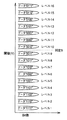
図31は、書込動作の第1の処理ステップにおける各ラッチに保持されるデータを示し、図32は、書込動作の第1の処理ステップにおけるメモリセルのしきい値と判定レベルを示す。
【0190】
図33は、書込動作の第2の処理ステップにおける各ラッチに保持されるデータを示し、図34は、書込動作の第2の処理ステップにおけるメモリセルのしきい値と判定レベルを示す。
【0191】
図35は、書込動作の第3の処理ステップにおける各ラッチに保持されるデータを示し、図36は、書込動作の第3の処理ステップにおけるメモリセルのしきい値と判定レベルを示す。
【0192】
まず、書込動作が行われるメモリセルブロックについては、全てのメモリセルについてデータ“11”に対応するしきい値とされる。
【0193】
次に、図31および図32を参照して、書込動作の第1の処理ステップにおいては、入力されたデータ(1/2セクタ分:16進表現でC9h)をデータラッチDL−Lに格納し、センスラッチSLに転送する。第2の判定レベルVj2に基づいて、レベル3に相当するしきい値までの書込みを行う。この第2の判定レベルVj2での書込み動作中に、残りの1/2セクタ分のデータ(16進表現で93h)がデータラッチDL−Rに格納される。
【0194】
次に、図33および図34を参照して、書込動作の第2の処理ステップにおいては、書込データ変換回路230は、データラッチDL−R、DL−Lに含まれるデータについて、対応するビットデータの組について演算することで、データラッチDL−Lに保持されるビットが“0”であって、データラッチDL−Rに保持されるビットが“1”となっているデータに対応するセンスラッチSLのビットデータのみを“0”レベルとする。
【0195】
図33に示すとおり、このような演算を行なった後には、センスラッチSLには、“10110111”というデータが保持されている。このようにしてセンスラチSLに保持されたデータに基づいて、センスラッチSLの各ビットにそれぞれ対応するメモリセルMC0〜MC7にデータの書込が行なわれる。ここで、メモリセルMC0〜MC7は、同一のワード線WLに接続している。さらに、ベリファイ動作の判定値としては第3番目の判定値Vj3を用いる。
【0196】
このとき、センスラッチ中のデータ“0”に対応するメモリセルに対してデータの書込みが行なわれる。したがって、センスラッチの第1ビットと第4ビットに対応するメモリセルMC1およびMC4に対してレベル4のデータ(データ“01”に対応する)の書込が行なわれる。
【0197】
データの書込は、ワード線WLに高電圧を印加することで、FN(ファウラー・ノルドハイム)トンネル電流を利用して書込まれる。
【0198】
センスラッチSLのビットデータが“1”のビットに対応するビット線BLにはワード線WLから印加される電圧を緩和するために、ワード線電圧以下の電圧が印加される。結果的に、センスラッチに保持されるビットデータが“0”に対応するビット線BLに接続するメモリセルにだけデータの書込が行なわれる。
【0199】
次に、図35および36を参照して、書込動作の第3ステップでは、書込みデータ変換回路230は、データラッチDL−R、DL−Lに保持されたデータの演算を行ない、データラッチDL−Lに保持されたビットデータが“1”であり、データラッチDL−Rに保持されたビットデータが“0”であるデータの組に対応するセンスラッチSLのビットには“0”が書込まれる。ベリファイ動作における判定値を第1の判定レベルVj1に変えたうえで、メモリセルMC3およびMC6にのみデータの書込が行なわれる。
【0200】
以上の説明から明らかなように、図31および図32の書込みでは、本来レベル4としてデータが書込まれるべきメモリセルに対しても、一旦、レベル3としてデータの書込みが行われている。図33および図34で、レベル4としての書き込みが行われるメモリセルは、すべて図31および図32において、レベル3として書込みが行われたメモリセルに含まれる。
【0201】
同様に、図35および図36において、レベル2としての書き込みが行われるメモリセルも、その直前まで、レベル1のしきい値を有していたメモリセルの中に含まれている。
【0202】
つまり、図31および図32の書込みを行う時点で、レベル4および3の書込みが行われるメモリセルと、メモリ2および1の書込みが行われるメモリセルとが分離されていることになる。
【0203】
したがって、実施の形態3の4値フラッシュメモリでは、書込みコマンドの入力後、データラッチDL−Rへの1/2セクタ分のデータの入力時間中にすでに書込み動作が開始されているため、書込み時間を短縮することが可能である。
【0204】
特に、以下の式(2)の条件を満たす場合は、短縮の効果が大きい。
{セクタサイズ(Byte)×(1Byte当りの入力時間)×1/2}≧{レベル3の書込み時間} …(2)
図37は、実施の形態3のフラッシュメモリ1000の書込動作を説明するためのタイミングチャートである。
【0205】
図37を参照して、時刻t1において、まず、1/2セクタ分のデータ(上位ビットのデータ)の入力が開始され、時刻t2からデータラッチDL−Lへの格納が始まる。
【0206】
時刻t3において、前半の1/2セクタ分のデータの入力が終了すると、データラッチDL−Lに格納されているデータは、センスラッチSLに転送される。
【0207】
一方、時刻t3において、1/2セクタ分のデータ(下位ビットのデータ)の入力が開始され、時刻t4からデータラッチDL−Rへの格納が始まる。
【0208】
時刻t5において、センスラッチSLに格納されたデータに基づいて、第2の判定レベルVj2に応じて、書込み動作が行なわれる。
【0209】
時刻t6において、第2の判定レベルでの書き込み動作が終了すると、センスラッチSLはクリアされる。
【0210】
時刻t7において、書込みデータ変換回路230は、データラッチDL−R、DL−Lに含まれるデータについて、対応するビットデータの組について演算を開始し、時刻t8から、データラッチDL−Lに保持されるビットが“0”であって、データラッチDL−Rに保持されるビットが“1”となっているデータに対応するセンスラッチSLのビットデータのみを“0”レベルとしていく。
【0211】
時刻t9において、センスラッチSLに格納されたデータに基づいて、第3の判定レベルVj3に応じて、書込み動作が行なわれる。
【0212】
時刻t10において、第3の判定レベルでの書き込み動作が終了すると、センスラッチSLはクリアされる。
【0213】
時刻t11において、書込みデータ変換回路230は、データラッチDL−R、DL−Lに保持されたデータの演算を開始し、時刻t12から、データラッチDL−Lに保持されたビットデータが“1”であり、データラッチDL−Rに保持されたビットデータが“0”であるデータの組に対応するセンスラッチSLのビットに“0”を書込んでいく。
【0214】
時刻t13において、センスラッチSLに格納されたデータに基づいて、第1の判定レベルVj1に応じて、書込み動作が行なわれる。
【0215】
以上説明したとおり、時刻t1において入力されたデータ列の書込みが行なわれている期間中に、このデータ列に続いて書込まれるべきデータ列の格納動作が完了しているために、4値メモリセルへデータを書込む際の遅延時間を削減することが可能である。
【0216】
[実施の形態3の変形例]
実施の形態3の書込み動作では、書込み時間の短縮を可能とした。一方で、書込み動作時に使用されるデータラッチの個数を削減することも可能である。
【0217】
図38および39は、本発明の実施の形態3変形例の動作説明図であり、書込動作の第2の処理ステップにおいて、データラッチDL−LおよびDL−RならびにセンスラッチSLに保持されるデータおよび読出時のメモリセルのしきい値と判定レベルを示す概念図である。
【0218】
図38は、書込動作の第2の処理ステップにおける各ラッチに保持されるデータを示し、図39は、書込動作の第2の処理ステップにおける読出し動作のメモリセルのしきい値と判定レベルを示す。
【0219】
まず、図31および図32と同様に、書込み動作の第1の処理ステップで、メモリセルにデータを書込む。
【0220】
つづいて、書込み動作の第2の処理ステップで、残りの1/2セクタ分のデータを再び、データラッチDL−Lに取り込む。一方、第2の判定レベルVj2で第1の処理ステップでメモリセルに書込んだデータを読出し、センスラッチSLに格納する。書込みデータ変換回路230は、データラッチDL−Lに保持されたデータとセンスラッチSLに保持されたデータとの間で、図33および図34におけるのと同様の演算を行い、センスラッチSLの内容を書き換える。このセンスラッチSLのデータに基づいて、第3の判定レベルVj3に応じた書込み動作を実行する。
【0221】
つづいて、同様に、再び、第2の判定レベルVj2でメモリセルに書込んだデータを読出し、センスラッチSLに格納する。書込みデータ変換回路230は、データラッチDL−Lに保持されたデータとセンスラッチSLに保持されたデータとの間で、図35および図36におけるのと同様の演算を行い、センスラッチSLの内容を書き換える。このセンスラッチSLのデータに基づいて、第1の判定レベルVj1に応じた書込み動作を実行する。
【0222】
以上のような動作により、データ書込みに必要となるデータラッチの個数を削減することが可能となる。
【0223】
[実施の形態4]
実施の形態4の書込み動作では、実施の形態3の書込み動作に要する時間をさらに削減するために、実施の形態3において、図33および図34で説明した判定値レベルVj3での書込みと、図35および図36で説明した判定値レベルVj1での書込みとを同時に行うことが可能な書込み処理を提供する。
【0224】
実施の形態3の書込み処理では、判定値レベルVj3でのしきい値レベル4への書込み、判定値レベルVj2でのしきい値レベル3への書込み、判定値レベルVj1でのしきい値レベル2への書込み処理においては、表1に示すように、データの書込みを行わないメモリセルのドレインには、書込み阻止電圧を印加している。
【0225】
【表1】

図40および41は、本発明の実施の形態4の動作説明図であり、書込動作の第2の処理ステップにおいて、データラッチDL−LおよびDL−RならびにセンスラッチSLに保持されるデータおよび書込時のメモリセルのしきい値と判定レベルを示す概念図である。
【0227】
図40は、書込動作の第2の処理ステップにおける各ラッチに保持されるデータを示し、図41は、書込動作の第2の処理ステップにおける書込み動作のメモリセルのしきい値と判定レベルを示す。
【0228】
まず、図31および図32と同様に、書込み動作の第1の処理ステップで、メモリセルに第2の判定レベルVj2に基づいてデータを書込む。
【0229】
つづいて、書込み動作の第2の処理ステップで、残りの1/2セクタ分のデータを、データラッチDL−Rに取り込む。書込データ変換回路230は、データラッチDL−R、DL−Lに含まれるデータについて、対応するビットデータの組について演算することで、データラッチDL−Lに保持されるビットデータと、データラッチDL−Rに保持されるビットデータとが異なっている場合にのみ、対応するセンスラッチSLのビットデータを“0”レベルとする。これは、データラッチDL−RとDL−Lに保持される各ビットデータの排他的論理和演算結果の反転処理を行うことに相当する。
【0230】
このようにして書換えられたセンスラッチSLの値に基づいて、以下の表2の条件を満たすように、メモリセルにデータを書込む。すなわち、データの書込みを行うメモリセルに対しては、書込むデータが“01”であるか、“10”であるかに応じて、表2のとおりにドレイン電圧を変化させる。
【0231】
【表2】
表2においては、電圧V1<電圧V2<電圧V3の関係が成り立つ。メモリセルトランジスタのしきい値電圧の設定値異なる場合は、電圧V1、V2、V3はこの関係を維持しつつ、電圧V2、V3の値を変化させればよい。
【0233】
以上のような動作により、データ書込みに必要となる時間を一層削減することが可能となる。
【0234】
[実施の形態5]
以上の説明では、1つのメモリセルに保持されるデータが、2ビット、つまり、4値の場合において、データの読出、書込みの動作について説明した。
【0235】
より一般的に、n≧m+1、m≧0、n,mは自然数とするとき、1つのメモリセルに保持されるデータが2n値の場合は、書込みデータと書込みデータに対応するメモリセルトランジスタのしきい値のレベルとの対応づけに一定の関係をおくとき、各メモリセルに保持されるnビットデータのうち、第2n-1の判定レベルでの読出で、nビットのうちの1ビット(たとえば、最上位の1ビット)が確定するようにできる。
【0236】
さらに、第2n-2の判定レベルと第(2n-1+2n-2)の判定レベルの2つでの読出処理により、nビットのうちのさらに1ビットが確定するようにできる。
【0237】
さらに、第Σ(2n-1-m+Y)の判定レベル(Σは、YについてY=0からY=mまでの和:m≧0、n≧m+1)等の2m個の判定レベルでの読出処理により、nビットのうちのさらに1ビットが確定するようにできる。
【0238】
最終的に、第1の判定レベル、第3の判定レベル、第5の判定レベル、…、第2n-1の判定レベルでの読出処理により、nビットのうちのさらに1ビットが確定するようにできる。
【0239】
図42は、3ビット、すなわち、8値のデータを1つのメモリセルに書込む場合に、上述の要領で読出が可能なときの書込みデータと書込みデータに対応するメモリセルトランジスタのしきい値のレベルとの対応づけを示す図である。
【0240】
第4の判定レベルでの読出で最上位ビットが確定し、第2および第6の判定レベルでの読出で中位ビットが確定し、第1、3、5、7の判定レベルでの読出で最下位ビットが確定する。
【0241】
これに対して、図43は、3ビット、すなわち、8値のデータを1つのメモリセルに書込む場合に、上述の要領で読出ができないときの書込みデータと書込みデータに対応するメモリセルトランジスタのしきい値のレベルとの対応づけを示す図である。
【0242】
第4の判定レベルでの読出で最上位ビットが確定するものの、第2および第6の判定レベルでの読出では中位ビットは確定しない。
【0243】
[16値データの読出動作]
以下では、16(=2n:n=4)値の場合を例にとって、読出動作を説明する。以下に説明するとおり、データラッチ回路が、回路DL−LとDL−Rの2系統から、回路DL−1〜4の4系統となり、制御回路210の動作が異なる以外は、本実施の形態のフラッシュメモリの構成は、実施の形態1のフラッシュメモリ1000の構成と同様である。
【0244】
図44〜81は、本発明の実施の形態5の動作説明図であり、読出動作の第1〜第19の処理ステップにおいて、データラッチDL−1〜DL−4ならびにセンスラッチSLに保持されるデータおよび読出時のメモリセルのしきい値と判定レベルを示す概念図である。
【0245】
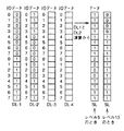
図44は、読出動作の第1の処理ステップにおける各ラッチに保持されるデータを示し、図45は、読出動作の第1の処理ステップにおけるメモリセルのしきい値と判定レベルを示す。
【0246】
まず、図44および図45を参照して、読出動作の第1の処理ステップにおいては、同一のワード線に接続された複数メモリセル、たとえば、1kByte分のメモリセルから、第8(=2n-1:n=4)の判定レベルVj8で一括して読出を行ない、その結果をセンスラッチ回路120に格納する。
【0247】
図44では、センスラッチ回路120中において、1セクタ分の読出動作で、最初にデータ入出力端子群10から出力される2バイト分のデータを保持するセンスラッチSLと、これに対応するデータラッチDL−1〜DL−4を抜き出して示す。1セクタ分の読出動作で、この2バイト分のデータに続いてデータ入出力端子群10から読み出されるデータについても、以下に説明するのと同様の処理が並行して行なわれている。
【0248】
このデータ入出力端子群10から最初に出力される1バイト分のデータを含むデータ列を保持するメモリセル列MC0〜MC15には、それぞれデータ“0111”,“0110”,“0100”,“0101”,“0001”,“0000”,“0010”,“0011”,“1011”,“1010”,“1000”,“1001”,“1101”,“1100”,“1110”,“1111”が保持されているものとする。
【0249】
図45に示すように、メモリセルのしきい値の高い側のレベル16から低い側のレベル1までのレベルにそれぞれ対応する書込みデータは、“0111”,“0110”,“0100”,“0101”,“0001”,“0000”,“0010”,“0011”,“1011”,“1010”,“1000”,“1001”,“1101”,“1100”,“1110”,“1111”であるものとする。
【0250】
したがって、図44において、センスラッチ回路120の2バイト分の領域に保持されるデータは、16進数表示で、00hとFFhである。
【0251】
第8の判定レベルVj8で一括して読出されたデータは、センスラッチSLからデータラッチDL−1に格納される。この時点で、制御回路210の制御により、データラッチDL−1に格納されたデータが、順次1バイトずつ(または2バイトずつ)データ入出力端子群10から出力される。
【0252】
このように、読出動作の第1の処理ステップにおいて、第8の判定レベルVj2で読出動作をまず行なうのは、図45に示すとおり、このレベルで読出すことにより、メモリセル内の16種のデータが、“0”または“1”のうちのいずれであるかが確定するからである。すなわち、メモリセルMC0〜MC15に格納されるデータの最上位のビットの0または1が確定することになる。
【0253】
図46は、読出動作の第2の処理ステップにおける各ラッチに保持されるデータを示し、図47は、読出動作の第2の処理ステップにおけるメモリセルのしきい値と判定レベルを示す。
【0254】
次に、図46および図47を参照して、読出動作の第2の処理ステップにおいては、第1の処理ステップでセンスラッチSLからデータラッチDL−1にデータを格納し、センスラッチSLがクリアされた時点で、第4(=2n-2:n=4)の判定レベルVj4で読出動作を行ない、読み出されたデータをセンスラッチ回路120に格納する。つまり、データラッチ回路DL−1からはデータ出力を行なっている途中で、センスラッチSLからデータラッチDL−2にデータ転送を行なう。データラッチDL−2へのデータ転送後、センスラッチ回路120はクリアされる。
【0255】
図48は、読出動作の第3の処理ステップにおける各ラッチに保持されるデータを示し、図49は、読出動作の第3の処理ステップにおけるメモリセルのしきい値と判定レベルを示す。
【0256】
次に、図48および図49を参照して、読出動作の第3の処理ステップにおいては、第12(=2n-1+2n-2:n=4)の判定レベルVj12で読出動作を行ない、センスラッチ回路120にデータを格納する。読出データ変換回路220は、センスラッチSLに保持されるデータの反転データとデータラッチDL−2に保持されるデータとの間でNOR演算を行なった結果にしたがって、データラッチDL2内のデータビットを変更する。
【0257】
図50は、読出動作の第4の処理ステップにおける各ラッチに保持されるデータを示し、図51は、読出動作の第4の処理ステップにおけるメモリセルのしきい値と判定レベルを示す。
【0258】
次に、図50および図51を参照して、読出動作の第4の処理ステップにおいては、第3の処理ステップでセンスラッチSLからデータラッチDL−1にデータを格納し、センスラッチSLがクリアされた時点で、第2(=2n-3:n=4)の判定レベルVj2で読出動作を行ない、読み出されたデータをセンスラッチ回路120に格納する。データラッチ回路DL−1からはデータ出力を行ない、その出力後にはデータラッチ回路DL−2からデータ出力を行なっている間に、センスラッチSLからデータラッチDL−3にデータ転送を行なう。データラッチDL−3へのデータ転送後、センスラッチ回路120はクリアされる。
【0259】
図52は、読出動作の第5の処理ステップにおける各ラッチに保持されるデータを示し、図53は、読出動作の第5の処理ステップにおけるメモリセルのしきい値と判定レベルを示す。
【0260】
次に、図52および図53を参照して、読出動作の第5の処理ステップにおいては、第6(=2n-2+2n-3:n=4)の判定レベルVj6で読出動作を行ない、センスラッチ回路120にデータを格納する。読出データ変換回路220は、センスラッチSLに保持されるデータの反転データとデータラッチDL−3に保持されるデータとの間でNOR演算を行なった結果にしたがって、データラッチDL3内のデータビットを変更する。
【0261】
図54は、読出動作の第6の処理ステップにおける各ラッチに保持されるデータを示し、図55は、読出動作の第6の処理ステップにおけるメモリセルのしきい値と判定レベルを示す。
【0262】
次に、図54および図55を参照して、読出動作の第6の処理ステップにおいては、第5の処理ステップでセンスラッチSLからデータラッチDL−3にデータを格納し、センスラッチSLがクリアされた時点で、第10(=2n-1+2n-3:n=4)の判定レベルVj10で読出動作を行ない、読み出されたデータをセンスラッチ回路120に格納する。データラッチ回路DL−1からはデータ出力を行ない、その出力後にはデータラッチ回路DL−2からデータ出力を行なっている間に、センスラッチSLからデータラッチDL−4にデータ転送を行なう。データラッチDL−4へのデータ転送後、センスラッチ回路120はクリアされる。
【0263】
図56は、読出動作の第7の処理ステップにおける各ラッチに保持されるデータを示し、図57は、読出動作の第7の処理ステップにおけるメモリセルのしきい値と判定レベルを示す。
【0264】
次に、図56および図57を参照して、読出動作の第7の処理ステップにおいては、第14(=2n-1+2n-2+2n-3:n=4)の判定レベルVj14で読出動作を行ない、センスラッチ回路120にデータを格納する。読出データ変換回路220は、センスラッチSLに保持されるデータの反転データとデータラッチDL−4に保持されるデータとの間でNOR演算を行なった結果にしたがって、データラッチDL4内のデータビットを変更する。
【0265】
図58は、読出動作の第8の処理ステップにおける各ラッチに保持されるデータを示し、図59は、読出動作の第8の処理ステップにおけるメモリセルのしきい値と判定レベルを示す。
【0266】
次に、図58と図59を参照して、読出データ変換回路220は、データラッチDL−3とDL−4に保持されたビットデータ間でOR演算を行ない、結果をデータラッチ回路DL−3に格納する。
【0267】
図60は、読出動作の第9の処理ステップにおける各ラッチに保持されるデータを示し、図61は、読出動作の第9の処理ステップにおけるメモリセルのしきい値と判定レベルを示す。
【0268】
次に、図60と図61を参照して、データラッチDL−2からのデータ出力中において、第1(=2n-4:n=4)の判定レベルVj1で読出動作を行ない、センスラッチ回路120にデータを格納する。センスラッチSL中のデータをデータラッチDL−4に転送する。なお、読出データ変換回路220は、データラッチDL−2からのデータ出力が終了後、データラッチDL−3に保持されるデータの反転データをデータ入出力端子に出力する。
【0269】
図62は、読出動作の第10の処理ステップにおける各ラッチに保持されるデータを示し、図63は、読出動作の第10の処理ステップにおけるメモリセルのしきい値と判定レベルを示す。
【0270】
次に、図62および図63を参照して、読出動作の第10の処理ステップにおいては、第3(=2n-3+2n-4:n=4)の判定レベルVj3で読出動作を行ない、センスラッチ回路120にデータを格納する。読出データ変換回路220は、センスラッチSLに保持されるデータの反転データとデータラッチDL−4に保持されるデータとの間でNOR演算を行なった結果にしたがって、データラッチDL4内のデータビットを変更する。
【0271】
図64は、読出動作の第11の処理ステップにおける各ラッチに保持されるデータを示し、図65は、読出動作の第11の処理ステップにおけるメモリセルのしきい値と判定レベルを示す。
【0272】
次に、図64と図65を参照して、データラッチDL−2からのデータ出力中において、第5(=2n-2+2n-4:n=4)の判定レベルVj5で読出動作を行ない、センスラッチ回路120にデータを格納する。センスラッチSL中のデータをデータラッチDL−1に転送する。
【0273】
図66は、読出動作の第12の処理ステップにおける各ラッチに保持されるデータを示し、図67は、読出動作の第12の処理ステップにおけるメモリセルのしきい値と判定レベルを示す。
【0274】
次に、図66および図67を参照して、読出動作の第12の処理ステップにおいては、第7(=2n-2+2n-3+2n-4:n=4)の判定レベルVj7で読出動作を行ない、センスラッチ回路120にデータを格納する。読出データ変換回路220は、センスラッチSLに保持されるデータの反転データとデータラッチDL−1に保持されるデータとの間でNOR演算を行なった結果にしたがって、データラッチDL1内のデータビットを変更する。
【0275】
図68は、読出動作の第13の処理ステップにおける各ラッチに保持されるデータを示し、図69は、読出動作の第13の処理ステップにおけるメモリセルのしきい値と判定レベルを示す。
【0276】
次に、図68と図69を参照して、読出データ変換回路220は、データラッチDL−1とDL−4に保持されたビットデータ間でOR演算を行ない、結果をデータラッチ回路DL−4に格納する。
【0277】
図70は、読出動作の第14の処理ステップにおける各ラッチに保持されるデータを示し、図71は、読出動作の第14の処理ステップにおけるメモリセルのしきい値と判定レベルを示す。
【0278】
次に、図70と図71を参照して、データラッチDL−2またはDL3からのデータ出力中において、第9(=2n-1+2n-4:n=4)の判定レベルVj9で読出動作を行ない、センスラッチ回路120にデータを格納する。センスラッチSL中のデータはデータラッチDL−1に転送される。
【0279】
図72は、読出動作の第15の処理ステップにおける各ラッチに保持されるデータを示し、図73は、読出動作の第15の処理ステップにおけるメモリセルのしきい値と判定レベルを示す。
【0280】
次に、図72および図73を参照して、読出動作の第15の処理ステップにおいては、第11(=2n-1+2n-3+2n-4:n=4)の判定レベルVj11で読出動作を行ない、センスラッチ回路120にデータを格納する。読出データ変換回路220は、センスラッチSLに保持されるデータの反転データとデータラッチDL−1に保持されるデータとの間でNOR演算を行なった結果にしたがって、データラッチDL1内のデータビットを変更する。
【0281】
図74は、読出動作の第16の処理ステップにおける各ラッチに保持されるデータを示し、図75は、読出動作の第16の処理ステップにおけるメモリセルのしきい値と判定レベルを示す。
【0282】
次に、図74と図75を参照して、読出データ変換回路220は、データラッチDL−1とDL−4に保持されたビットデータ間でOR演算を行ない、結果をデータラッチ回路DL−4に格納する。
【0283】
図76は、読出動作の第17の処理ステップにおける各ラッチに保持されるデータを示し、図77は、読出動作の第17の処理ステップにおけるメモリセルのしきい値と判定レベルを示す。
【0284】
次に、図76と図77を参照して、データラッチDL−2またはDL3からのデータ出力中において、第13(=2n-1+2n-2+2n-4:n=4)の判定レベルVj13で読出動作を行ない、センスラッチ回路120にデータを格納する。センスラッチSL中のデータはデータラッチDL−1に転送される。
【0285】
図78は、読出動作の第18の処理ステップにおける各ラッチに保持されるデータを示し、図79は、読出動作の第18の処理ステップにおけるメモリセルのしきい値と判定レベルを示す。
【0286】
次に、図78および図79を参照して、読出動作の第18の処理ステップにおいては、第15(=2n-1+2n-2+2n-3+2n-4:n=4)の判定レベルVj15で読出動作を行ない、センスラッチ回路120にデータを格納する。読出データ変換回路220は、センスラッチSLに保持されるデータの反転データとデータラッチDL−1に保持されるデータとの間でNOR演算を行なった結果にしたがって、データラッチDL1内のデータビットを変更する。
【0287】
図80は、読出動作の第19の処理ステップにおける各ラッチに保持されるデータを示し、図81は、読出動作の第19の処理ステップにおけるメモリセルのしきい値と判定レベルを示す。
【0288】
次に、図80と図81を参照して、読出データ変換回路220は、データラッチDL−1とDL−4に保持されたビットデータ間でOR演算を行ない、結果をデータラッチ回路DL−4に格納する。
【0289】
データラッチDL−3のデータ出力が終了した後、制御回路210は、データラッチDL−4に保持されるデータの反転データをデータ入出力端子群10へ出力を開始する。
【0290】
以上のような動作により、16値のデータを保持できるメモリセルからのデータ読出時間を短縮することが可能である。
【0291】
なお、以上の説明では、判定レベルの低い方から2つずつ組にして、各組の上位の判定レベル値を反転し、2つの判定結果をNOR処理し、最後に各組の結果をOR処理している。この発明は、このような構成に限られるわけではなく、たとえば、判定レベルの高い方から2つずつ組にしても良い。
【0292】
[16値データの書込み動作]
つぎに、データの書込み動作について説明する。
【0293】
図82〜87は、書込動作の第1〜第7の処理ステップにおいて、データラッチDL−1〜DL−4ならびにセンスラッチSLに保持されるデータおよび書込時のメモリセルのしきい値と判定レベルを示す概念図である。
【0294】
図82は、書込動作の第1の処理ステップにおける各ラッチに保持されるデータを示し、図83は、書込動作の第1の処理ステップにおけるメモリセルのしきい値と判定レベルを示す。
【0295】
図84は、書込動作の第2および3の処理ステップにおける各ラッチに保持されるデータを示し、図85は、書込動作の第2および3の処理ステップにおけるメモリセルのしきい値と判定レベルを示す。
【0296】
図86は、書込動作の第4〜7の処理ステップにおける各ラッチに保持されるデータを示し、図87は、書込動作の第4〜7の処理ステップにおけるメモリセルのしきい値と判定レベルを示す。
【0297】
まず、書込動作が行われるメモリセルブロックについては、全てのメモリセルについてデータ“1111”に対応するしきい値とされる。
【0298】
次に、図82および図83を参照して、書込動作の第1の処理ステップにおいては、入力されたデータ(16進表現で00hとFFh)をデータラッチDL−1に格納し、センスラッチSLに転送する。第8の判定レベルVj8に基づいて、レベル9に相当するしきい値までの書込みを行う。この第8の判定レベルVj8での書込み動作中に、残りのデータのうち2バイト分のデータがさらにデータラッチDL−2に格納される。
【0299】
次に、図84および図85を参照して、書込動作の第2の処理ステップにおいては、書込データ変換回路230は、データラッチDL−1、DL−2に含まれるデータについて、対応するビットデータの組について演算することで、データラッチDL−1に保持されるビットが“1”であって、データラッチDL−2に保持されるビットが“0”となっているデータに対応するセンスラッチSLのビットデータのみを“0”レベルとする。
【0300】
このようにしてセンスラチSLに保持されたデータに基づいて、センスラッチSLの各ビットにそれぞれ対応するメモリセルMC0〜MC15にデータの書込が行なわれる。ここで、メモリセルMC0〜MC15は、同一のワード線WLに接続している。さらに、ベリファイ動作の判定値としては第4番目の判定値Vj4を用い、しきい値レベルのレベル5まで書込みを行なう。
【0301】
このとき、センスラッチ中のデータ“0”に対応するメモリセルに対してデータの書込みが行なわれる。
【0302】
データの書込は、ワード線WLに高電圧を印加することで、FN(ファウラー・ノルドハイム)トンネル電流を利用して書込まれる。
【0303】
センスラッチSLのビットデータが“1”のビットに対応するビット線BLにはワード線WLから印加される電圧を緩和するために、ワード線電圧以下の電圧が印加される。結果的に、センスラッチに保持されるビットデータが“0”に対応するビット線BLに接続するメモリセルにだけデータの書込が行なわれる。
【0304】
さらに、図84および図85を参照して、書込動作の第3の処理ステップにおいては、書込データ変換回路230は、データラッチDL−1、DL−2に含まれるデータについて、対応するビットデータの組について演算することで、データラッチDL−1に保持されるビットが“0”であって、データラッチDL−2に保持されるビットが“1”となっているデータに対応するセンスラッチSLのビットデータのみを“0”レベルとする。
【0305】
このようにしてセンスラチSLに保持されたデータに基づいて、センスラッチSLの各ビットにそれぞれ対応するメモリセルMC0〜MC15にデータの書込が行なわれる。ここで、ベリファイ動作の判定値としては第12番目の判定値Vj12を用い、しきい値レベルのレベル13まで書込みが行なわれる。
【0306】
この第12の判定レベルVj12での書込み動作中に、残りの1/4セクタ分のデータがデータラッチDL−3に格納される。
【0307】
次に、図86および図87を参照して、書込動作の第4の処理ステップにおいては、書込データ変換回路230は、データラッチDL−1、DL−2、DL−3に含まれるデータについて、対応するビットデータの組について演算することで、データラッチDL−1に保持されるビットが“1”、データラッチDL−2に保持されるビットが“1”であって、データラッチDL−3に保持されるビットが“0”となっているデータに対応するセンスラッチSLのビットデータのみを“0”レベルとする。
【0308】
このようにしてセンスラチSLに保持されたデータに基づいて、センスラッチSLの各ビットにそれぞれ対応するメモリセルMC0〜MC15にデータの書込が行なわれる。ここで、ベリファイ動作の判定値としては第2番目の判定値Vj2を用い、しきい値レベルのレベル3にまで書込みが行なわれる。
【0309】
さらに、図86および図87を参照して、書込動作の第5の処理ステップにおいては、書込データ変換回路230は、データラッチDL−1、DL−2およびDL−3に含まれるデータについて、対応するビットデータの組について演算することで、データラッチDL−1に保持されるビットが“1”、データラッチDL−2に保持されるビットが“0”、であって、データラッチDL−3に保持されるビットが“1”となっているデータに対応するセンスラッチSLのビットデータのみを“0”レベルとする。
【0310】
このようにしてセンスラチSLに保持されたデータに基づいて、センスラッチSLの各ビットにそれぞれ対応するメモリセルMC0〜MC15にデータの書込が行なわれる。ここで、ベリファイ動作の判定値としては第6番目の判定値Vj6を用い、しきい値レベルのレベル7まで書込みが行なわれる。
【0311】
以下同様にして、書込動作の第6の処理ステップにおいては、データラッチDL−1、DL−2、DL−3に保持されるデータのビットデータの組が、(0,0,0)に相当するセンスラッチのビットデータが“0”とされる。その上で、ベリファイ動作の判定値としては第10番目の判定値Vj10を用い、しきい値レベルのレベル11まで書込みが行なわれる。
【0312】
書込動作の第7の処理ステップにおいては、データラッチDL−1、DL−2、DL−3に保持されるデータのビットデータの組が、(0,1,1)に相当するセンスラッチのビットデータが“0”とされる。その上で、ベリファイ動作の判定値としては第14番目の判定値Vj14を用い、しきい値レベルのレベル15まで書込みが行なわれる。このレベル15までの書込み動作期間中に、データラッチ回路DL−4に、さらに残りの2バイトのデータが格納される。
【0313】
さらに、図示しないが、書込動作の第8〜15の処理ステップにおいては、それぞれ、データラッチDL−1、DL−2、DL−3、DL−4に保持されるデータのビットデータの組が、(1,1,1,0)、(1,1,0,1)、(1,0,0,0)、(1,0,1,1)、(0,0,1,0)、(0,0,0,1)、(0,1,0,0)、(0,1,1,1)に相当するセンスラッチのビットデータが“0”とされる。その上で、ベリファイ動作の判定値としては第1,3,5,7,9,11,13,15番目の判定値を用い、それぞれのステップに対応するしきい値レベルまで書込みが行なわれる。
【0314】
以上説明した通り、実施の形態5の16値フラッシュメモリでは、書込みコマンドの入力後、複数のデータラッチ回路のうちの少なくとも1つへのデータの入力時間中にすでに書込み動作が開始されているため、書込み時間を短縮することが可能である。
【0315】
[実施の形態6]
以上の説明では、データラッチ回路を4つとしたが、データラッチ回路の個数としては、データ出力用に1つ、データをNOR演算するために1つ、各ビット間でのOR演算を行なうための1つの計3つあれば、十分である。
【0316】
以下では、16値のメモリセルへのデータの書き込みにあたり、3個のデータラッチ回路DL−1〜DL−3でデータ書込みを行なう場合の処理の流れを説明する。
【0317】
図88〜117は、書込動作の第1〜第15の処理ステップにおいて、データラッチDL−1〜DL−3ならびにセンスラッチSLに保持されるデータおよび書込時のメモリセルのしきい値と判定レベルを示す概念図である。
【0318】
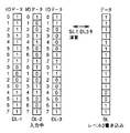
図88は、書込動作の第1の処理ステップにおける各ラッチに保持されるデータを示し、図89は、書込動作の第1の処理ステップにおけるメモリセルのしきい値と判定レベルを示す。
【0319】
まず、書込動作が行われるメモリセルブロックについては、全てのメモリセルについてデータ“1111”に対応するしきい値とされる。
【0320】
次に、図88および図89を参照して、書込動作の第1の処理ステップにおいては、入力されたデータ(16進表現で00hとFFh)をデータラッチDL−1に格納し、センスラッチSLに転送する。第8の判定レベルVj8に基づいて、レベル9に相当するしきい値までの書込みを行う。この後、データラッチDL−1はクリアされる。この第8の判定レベルVj8での書込み動作中に、残りのデータのうち2バイト分のデータがさらにデータラッチDL−2に格納される。
【0321】
ここで、再び、第8の判定レベルVj8で読出を行ない、読出データをセンスラッチSLに格納する。
【0322】
図90は、書込動作の第2の処理ステップにおける各ラッチに保持されるデータを示し、図91は、書込動作の第2の処理ステップにおけるメモリセルのしきい値と判定レベルを示す。
【0323】
次に、図90および図91を参照して、書込動作の第2の処理ステップにおいては、書込データ変換回路230は、センスラッチSLとデータラッチDL−2に含まれるデータについて、対応するビットデータの組について演算することで、センスラッチSLに保持されるビットが“1”であって、データラッチDL−2に保持されるビットが“0”となっているデータに対応するセンスラッチSLのビットデータのみを“0”レベルとする。
【0324】
このようにしてセンスラチSLに保持されたデータに基づいて、センスラッチSLの各ビットにそれぞれ対応するメモリセルMC0〜MC15にデータの書込が行なわれる。ここで、ベリファイ動作の判定値としては第4番目の判定値Vj4を用い、しきい値レベルのレベル1からレベル5まで書込みを行なう。
【0325】
さらに、図90および図91を参照して、書込動作の第2の処理ステップにおいても、第8の判定レベルVj8で読出を行ない、読出データをセンスラッチSLに格納する。書込データ変換回路230は、センスラッチ回路SL、DL−2に含まれるデータについて、対応するビットデータの組について演算することで、センスラッチSLに保持されるビットが“0”であって、データラッチDL−2に保持されるビットが“1”となっているデータに対応するセンスラッチSLのビットデータのみを“0”レベルとする。
【0326】
このようにしてセンスラッチSLに保持されたデータに基づいて、センスラッチSLの各ビットにそれぞれ対応するメモリセルMC0〜MC15に、第12の判定レベルVj12に応じてしきい値レベルのレベル9からレベル13まで書込みが行なわれる。
【0327】
一方、レベル13までのデータの書込みが行なわれている期間中に、データラッチDL−3に残りの2バイトのデータがさらに格納される。
【0328】
なお、上記書込動作の第2の処理ステップまでの動作では、判定レベルVj8での読出動作をその都度行なう代わりに、データラッチDL−1をクリアせずにデータを保持し、読出動作でセンスラッチSLに保持されるデータの代わりに、データラッチDL−1中のデータを用いても良い。ただし、以上の説明では、以下の手続きとの整合をとるために、判定レベルVj8での読出動作を行なうこととしている。
【0329】
図92は、書込動作の第3の処理ステップにおける各ラッチに保持されるデータを示し、図93は、書込動作の第3の処理ステップにおけるメモリセルのしきい値と判定レベルを示す。
【0330】
図92および図93を参照して、書込動作の第3の処理ステップにおいては、まず、第8の判定レベルVj8でデータの読出が行なわれ、読み出されたデータがセンスラッチSLに格納される。制御回路210は、センスラッチSLの反転データをデータラッチDL−1に転送する。
【0331】
図94は、書込動作の第4の処理ステップにおける各ラッチに保持されるデータを示し、図95は、書込動作の第4の処理ステップにおけるメモリセルのしきい値と判定レベルを示す。
【0332】
書込動作の第4の処理ステップにおいては、まず、第4の判定レベルVj4でデータの読出が行なわれ、読み出されたデータがセンスラッチSLに格納される。
【0333】
書込みデータ変換回路230は、センスラッチSLとデータラッチDL−1に含まれるデータについて、対応するビットデータの組についてOR演算した結果をデータラッチDL1に格納する。
【0334】
図96は、書込動作の第5の処理ステップにおける各ラッチに保持されるデータを示し、図97は、書込動作の第5の処理ステップにおけるメモリセルのしきい値と判定レベルを示す。
【0335】
書込みデータ変換回路230は、データラッチDL―3とセンスラッチSLとに含まれるデータについて、対応するビットデータの組について演算し、データラッチDL−3に保持されるビットが“1”であって、センスラッチSLに保持されるビットが“1”となっているデータに対応するセンスラッチSLのビットデータのみを“0”レベルとする。
【0336】
このようにしてセンスラチSLに保持されたデータに基づいて、判定レベルVj2をベリファイ電圧として、センスラッチSLの各ビットにそれぞれ対応するメモリセルMC0〜MC15に、しきい値レベルのレベル1からレベル3へデータの書込が行なわれる。
【0337】
この第2の判定レベルVj2での書込み動作中に、残りの2バイトのデータがデータラッチDL−2に格納される。
【0338】
図98は、書込動作の第6の処理ステップにおける各ラッチに保持されるデータを示し、図99は、書込動作の第6の処理ステップにおけるメモリセルのしきい値と判定レベルを示す。
【0339】
書込みデータ変換回路230は、データラッチDL―1とデータラッチDL−3とに含まれるデータについて、対応するビットデータの組について演算し、データラッチDL−1に保持されるビットが“0”であって、データラッチDL−3に保持されるビットが“1”となっているデータに対応するセンスラッチSLのビットデータのみを“0”レベルとする。
【0340】
このようにしてセンスラチSLに保持されたデータに基づいて、判定レベルVj6をベリファイ電圧として、センスラッチSLの各ビットにそれぞれ対応するメモリセルMC0〜MC15に、しきい値レベルのレベル5からレベル7へデータの書込が行なわれる。
【0341】
図100は、書込動作の第7の処理ステップにおける各ラッチに保持されるデータを示し、図101は、書込動作の第7の処理ステップにおけるメモリセルのしきい値と判定レベルを示す。
【0342】
書込み動作の第7の処理ステップでは、第8の判定レベルVj8でデータを読出し、センスラッチSLに格納後、制御回路210は、センスラッチSLからデータラッチDL−1にデータを転送する。
【0343】
図102は、書込動作の第8の処理ステップにおける各ラッチに保持されるデータを示し、図103は、書込動作の第8の処理ステップにおけるメモリセルのしきい値と判定レベルを示す。
【0344】
書込み動作の第8の処理ステップでは、第12の判定レベルVj12でデータを読出し、センスラッチSLに格納する。
【0345】
書込みデータ変換回路230は、センスラッチSLに保持されるデータの反転データとデータラッチDL−1とに含まれるデータについて、対応するビットデータの組についてOR演算し、演算結果をデータラッチDL−1に格納する。
【0346】
図104は、書込動作の第9の処理ステップにおける各ラッチに保持されるデータを示し、図105は、書込動作の第9の処理ステップにおけるメモリセルのしきい値と判定レベルを示す。
【0347】
書込みデータ変換回路230は、データラッチDL―1とデータラッチDL−3とに含まれるデータについて、対応するビットデータの組について演算し、データラッチDL−1に保持されるビットが“0”であって、データラッチDL−3に保持されるビットが“0”となっているデータに対応するセンスラッチSLのビットデータのみを“0”レベルとする。
【0348】
このようにしてセンスラチSLに保持されたデータに基づいて、判定レベルVj10をベリファイ電圧として、センスラッチSLの各ビットにそれぞれ対応するメモリセルMC0〜MC15に、しきい値レベルのレベル9からレベル11のデータの書込が行なわれる。
【0349】
図106は、書込動作の第10の処理ステップにおける各ラッチに保持されるデータを示し、図107は、書込動作の第10の処理ステップにおけるメモリセルのしきい値と判定レベルを示す。
【0350】
書込み動作の第10の処理ステップでは、第12の判定レベルVj12でデータが読出され、センスラッチSLに格納される。
【0351】
書込みデータ変換回路230は、センスラッチSLとデータラッチDL−3とに含まれるデータについて、対応するビットデータの組について演算し、センスラッチに保持されるビットが“0”であって、データラッチDL−3に保持されるビットが“1”となっているデータに対応するセンスラッチSLのビットデータのみを“0”レベルとする。
【0352】
図108は、書込動作の第11の処理ステップにおける各ラッチに保持されるデータを示し、図109は、書込動作の第11の処理ステップにおけるメモリセルのしきい値と判定レベルを示す。
【0353】
書込動作の第11の処理ステップにおいて、センスラチSLに保持されたデータに基づいて、判定レベルVj14をベリファイ電圧として、センスラッチSLの各ビットにそれぞれ対応するメモリセルMC0〜MC15に、しきい値レベルのレベル13からレベル15のデータの書込が行なわれる。
【0354】
図110は、書込動作の第12の処理ステップにおける各ラッチに保持されるデータを示し、図111は、書込動作の第12の処理ステップにおけるメモリセルのしきい値と判定レベルを示す。
【0355】
書込み動作の第12の処理ステップでは、第2の判定レベルVj2でデータが読出され、センスラッチSLに格納される。制御回路210は、センスラッチSLのデータをデータラッチDL1へ転送する。
【0356】
書込みデータ変換回路230は、センスラッチSLとデータラッチDL−2とに含まれるデータについて、対応するビットデータの組について演算し、センスラッチに保持されるビットが“1”であって、データラッチDL−2に保持されるビットが“0”となっているデータに対応するセンスラッチSLのビットデータのみを“0”レベルとする。
【0357】
図112は、書込動作の第13の処理ステップにおける各ラッチに保持されるデータを示し、図113は、書込動作の第13の処理ステップにおけるメモリセルのしきい値と判定レベルを示す。
【0358】
書込動作の第13の処理ステップにおいて、センスラチSLに保持されたデータに基づいて、判定レベルVj1をベリファイ電圧として、センスラッチSLの各ビットにそれぞれ対応するメモリセルMC0〜MC15に、しきい値レベルのレベル1からレベル2へのデータの書込が行なわれる。
【0359】
図114は、書込動作の第14の処理ステップにおける各ラッチに保持されるデータを示し、図115は、書込動作の第14の処理ステップにおけるメモリセルのしきい値と判定レベルを示す。
【0360】
書込み動作の第14の処理ステップでは、第4の判定レベルVj4でデータが読出され、センスラッチSLに格納される。
【0361】
書込みデータ変換回路230は、センスラッチSLに保持されるデータの反転データとデータラッチDL−1とに含まれるデータについて、対応するビットデータの組についてOR演算し、演算結果をデータラッチDL−1に格納する。
【0362】
図116は、書込動作の第15の処理ステップにおける各ラッチに保持されるデータを示し、図117は、書込動作の第15の処理ステップにおけるメモリセルのしきい値と判定レベルを示す。
【0363】
書込みデータ変換回路230は、データラッチDL1ととデータラッチDL−2とに含まれるデータについて、対応するビットデータの組について演算し、データラッチDL−1に保持されるビットが“0”であって、データラッチDL−2に保持されるビットが“1”となっているデータに対応するセンスラッチSLのビットデータのみを“0”レベルとする。
【0364】
このようにしてセンスラチSLに保持されたデータに基づいて、判定レベルVj3をベリファイ電圧として、センスラッチSLの各ビットにそれぞれ対応するメモリセルMC0〜MC15に、しきい値レベルのレベル3からレベル4へのデータの書込が行なわれる。
【0365】
以下同様にして、レベル6、8、10、12、14、16への書込みを行なう。
【0366】
すなわち、2値に識別できる判定レベルでの書込みを行ない、以下、各処理レベルにおいて、4値、8値、…、2n値に識別できるレベルでの書込みを行なう。各処理レベルでは、先に書込みを行なった判定レベル(たとえば、4値の処理レベルから8値の処理レベルになった場合には、4値を判別できる3つの判定レベル)のうちから2つずつ(上下端では1つ)を選んで読出を行ない、その処理レベルで書込みを行なうべきビットデータを確定し、書込みを行なう。
【0367】
以上説明した通り、実施の形態6の16値フラッシュメモリでは、データラッチ回路の個数を削減して、16値のデータを保持するメモリセルからのデータ書込みを行なう事が可能である。
【0368】
以上の説明では、判定レベルの低い方からデータの書込みを行なうこととしているが、逆に、判定レベルの高い方からデータの書込みを行なうこととしてもよい。
【0369】
なお、実施の形態4の4値メモリセルへの書込みと同様に、しきい値レベルのレベル5とレベル13までの書込み、レベル3とレベル11までの書込み、レベル7とレベル15までの書込み、レベル2とレベル10までの書込み、レベル4とレベル12までの書込み、レベル6とレベル14までの書込み、レベル8とレベル16までの書込みを、それぞれ同時に行なうことも可能である。これらの組合せでは、どれもしきい値電圧の上げ幅も、各々の組のレベル差(しきい値電圧差)も等しいため、同様のドレイン電圧の組を用いることが可能である。
【0370】
以上の説明では、16値のデータを格納するメモリセルを例として示したが、より一般に、2n値のデータを格納するメモリセルにも本発明を適用することが可能である。
【0371】
今回開示された実施の形態はすべての点で例示であって制限的なものではないと考えられるべきである。本発明の範囲は上記した説明ではなくて特許請求の範囲によって示され、特許請求の範囲と均等の意味および範囲内でのすべての変更が含まれることが意図される。
【0372】
【発明の効果】
以上のように、この発明によれば、1つのメモリセルに格納される多値データが、異なるタイミングで授受されるデータから生成されるので、読出動作では、各ビットデータの確定するごとにデータ出力を行なうことが可能で、データ出力時間を短縮できる。
【0373】
また、1つのメモリセルに格納される多値データが、異なるタイミングで授受されるデータから生成されるので、書込み動作では、各ビットデータの確定するごとにデータ書込みを行なうことが可能で、データ入力時間を短縮できる。
【図面の簡単な説明】
【図1】 本発明の実施の形態1の不揮発性半導体記憶装置であるフラッシュメモリ1000の構成を示す概略ブロック図である。
【図2】 読出動作の第1の処理ステップにおける各ラッチに保持されるデータを示ず図である。
【図3】 読出動作の第1の処理ステップにおけるメモリセルのしきい値と判定レベルを示す図である。
【図4】 読出動作の第2の処理ステップにおける各ラッチに保持されるデータを示す図である。
【図5】 読出動作の第2の処理ステップにおけるメモリセルのしきい値と判定レベルを示す図である。
【図6】 読出動作の第3の処理ステップにおける各ラッチに保持されるデータを示す図である。
【図7】 読出動作の第3の処理ステップにおけるメモリセルのしきい値と判定レベルを示す図である。
【図8】 実施の形態1のフラッシュメモリ1000の読出動作を説明するためのタイミングチャートである。
【図9】 1回の読出処理で、上位および下位ビットのいずれも確定できないような書込みレベルと書込みデータの対応付けの第1の例を示す図である。
【図10】 1回の読出処理で、上位および下位ビットのいずれも確定できないような書込みレベルと書込みデータの対応付けの第2の例を示す図である。
【図11】 1回の読出処理で、上位および下位ビットのいずれも確定できないような書込みレベルと書込みデータの対応付けの第3の例を示す図である。
【図12】 1回の読出処理で、上位および下位ビットのいずれも確定できないような書込みレベルと書込みデータの対応付けの第4の例を示す図である。
【図13】 実施の形態1の変形例2の読出動作の第2の処理ステップにおける各ラッチに保持されるデータを示す図である。
【図14】 実施の形態1の変形例2の読出動作の第2の処理ステップにおけるメモリセルのしきい値と判定レベルを示す図である。
【図15】 実施の形態1の変形例2のフラッシュメモリの読出動作を説明するためのタイミングチャートである。
【図16】 センスラッチ回路120とビット線との接続の切り換え方式の概念を示す図である。
【図17】 図16において示した概念を具体的に実現するための回路構成を示す図である。
【図18】 読出動作の第1の処理ステップにおける各ラッチに保持されるデータを示す図である。
【図19】 読出動作の第1の処理ステップにおけるメモリセルのしきい値と判定レベルを示す図である。
【図20】 読出動作の第2の処理ステップにおける各ラッチに保持されるデータを示す図である。
【図21】 読出動作の第2の処理ステップにおけるメモリセルのしきい値と判定レベルを示す図である。
【図22】 読出動作の第3の処理ステップにおける各ラッチに保持されるデータを示す図である。
【図23】 読出動作の第3の処理ステップにおけるメモリセルのしきい値と判定レベルを示す図である。
【図24】 読出動作の第4の処理ステップにおける各ラッチに保持されるデータを示す図である。
【図25】 読出動作の第4の処理ステップにおけるメモリセルのしきい値と判定レベルを示す図である。
【図26】 読出動作の第5の処理ステップにおける各ラッチに保持されるデータを示す図である。
【図27】 読出動作の第5の処理ステップにおけるメモリセルのしきい値と判定レベルを示す図である。
【図28】 読出動作の第6の処理ステップにおける各ラッチに保持されるデータを示す図である。
【図29】 読出動作の第6の処理ステップにおけるメモリセルのしきい値と判定レベルを示す図である
【図30】 実施の形態2のフラッシュメモリの読出動作を説明するためのタイミングチャートである。
【図31】 書込動作の第1の処理ステップにおける各ラッチに保持されるデータを示す図である。
【図32】 書込動作の第1の処理ステップにおけるメモリセルのしきい値と判定レベルを示す図である。
【図33】 書込動作の第2の処理ステップにおける各ラッチに保持されるデータを示す図である。
【図34】 書込動作の第2の処理ステップにおけるメモリセルのしきい値と判定レベルを示す図である。
【図35】 書込動作の第3の処理ステップにおける各ラッチに保持されるデータを示す図である。
【図36】 書込動作の第3の処理ステップにおけるメモリセルのしきい値と判定レベルを示す図である。
【図37】 実施の形態3のフラッシュメモリ1000の書込動作を説明するためのタイミングチャートである。
【図38】 書込動作の第2の処理ステップにおける各ラッチに保持されるデータを示す図である。
【図39】 書込動作の第2の処理ステップにおける読出し動作のメモリセルのしきい値と判定レベルを示す図である。
【図40】 書込動作の第2の処理ステップにおける各ラッチに保持されるデータを示す図である。
【図41】 書込動作の第2の処理ステップにおける書込み動作のメモリセルのしきい値と判定レベルを示す図である。
【図42】 実施の形態1の手順で書込み可能な書込みデータとメモリセルトランジスタのしきい値のレベルとの対応づけを示す図である。
【図43】 実施の形態1の手順で書込みできない書込みデータとメモリセルトランジスタのしきい値のレベルとの対応づけを示す図である。
【図44】 実施の形態5の読出動作の第1の処理ステップにおける各ラッチに保持されるデータを示す図である。
【図45】 実施の形態5の読出動作の第1の処理ステップにおけるメモリセルのしきい値と判定レベルを示す図である。
【図46】 実施の形態5の読出動作の第2の処理ステップにおける各ラッチに保持されるデータを示す図である。
【図47】 実施の形態5の読出動作の第2の処理ステップにおけるメモリセルのしきい値と判定レベルを示す図である。
【図48】 実施の形態5の読出動作の第3の処理ステップにおける各ラッチに保持されるデータを示す図である。
【図49】 実施の形態5の読出動作の第3の処理ステップにおけるメモリセルのしきい値と判定レベルを示す図である。
【図50】 実施の形態5の読出動作の第4の処理ステップにおける各ラッチに保持されるデータを示す図である。
【図51】 実施の形態5の読出動作の第4の処理ステップにおけるメモリセルのしきい値と判定レベルを示す図である。
【図52】 実施の形態5の読出動作の第5の処理ステップにおける各ラッチに保持されるデータを示す図である。
【図53】 実施の形態5の読出動作の第5の処理ステップにおけるメモリセルのしきい値と判定レベルを示す図である。
【図54】 実施の形態5の読出動作の第6の処理ステップにおける各ラッチに保持されるデータを示す図である。
【図55】 実施の形態5の読出動作の第6の処理ステップにおけるメモリセルのしきい値と判定レベルを示す図である。
【図56】 実施の形態5の読出動作の第7の処理ステップにおける各ラッチに保持されるデータを示す図である。
【図57】 実施の形態5の読出動作の第7の処理ステップにおけるメモリセルのしきい値と判定レベルを示す図である。
【図58】 実施の形態5の読出動作の第8の処理ステップにおける各ラッチに保持されるデータを示す図である。
【図59】 実施の形態5の読出動作の第8の処理ステップにおけるメモリセルのしきい値と判定レベルを示す図である。
【図60】 実施の形態5の読出動作の第9の処理ステップにおける各ラッチに保持されるデータを示す図である。
【図61】 実施の形態5の読出動作の第9の処理ステップにおけるメモリセルのしきい値と判定レベルを示す図である。
【図62】 実施の形態5の読出動作の第10の処理ステップにおける各ラッチに保持されるデータを示す図である。
【図63】 実施の形態5の読出動作の第10の処理ステップにおけるメモリセルのしきい値と判定レベルを示す図である。
【図64】 実施の形態5の読出動作の第11の処理ステップにおける各ラッチに保持されるデータを示す図である。
【図65】 実施の形態5の読出動作の第11の処理ステップにおけるメモリセルのしきい値と判定レベルを示す図である。
【図66】 実施の形態5の読出動作の第12の処理ステップにおける各ラッチに保持されるデータを示す図である。
【図67】 実施の形態5の読出動作の第12の処理ステップにおけるメモリセルのしきい値と判定レベルを示す図である。
【図68】 実施の形態5の読出動作の第13の処理ステップにおける各ラッチに保持されるデータを示す図である。
【図69】 実施の形態5の読出動作の第13の処理ステップにおけるメモリセルのしきい値と判定レベルを示す図である。
【図70】 実施の形態5の読出動作の第14の処理ステップにおける各ラッチに保持されるデータを示す図である。
【図71】 実施の形態5の読出動作の第14の処理ステップにおけるメモリセルのしきい値と判定レベルを示す図である。
【図72】 実施の形態5の読出動作の第15の処理ステップにおける各ラッチに保持されるデータを示す図である。
【図73】 実施の形態5の読出動作の第15の処理ステップにおけるメモリセルのしきい値と判定レベルを示す図である。
【図74】 実施の形態5の読出動作の第16の処理ステップにおける各ラッチに保持されるデータを示す図である。
【図75】 実施の形態5の読出動作の第16の処理ステップにおけるメモリセルのしきい値と判定レベルを示す図である。
【図76】 実施の形態5の読出動作の第17の処理ステップにおける各ラッチに保持されるデータを示す図である。
【図77】 実施の形態5の読出動作の第17の処理ステップにおけるメモリセルのしきい値と判定レベルを示す図である。
【図78】 実施の形態5の読出動作の第18の処理ステップにおける各ラッチに保持されるデータを示す図である。
【図79】 実施の形態5の読出動作の第18の処理ステップにおけるメモリセルのしきい値と判定レベルを示す図である。
【図80】 実施の形態5の読出動作の第19の処理ステップにおける各ラッチに保持されるデータを示す図である。
【図81】 実施の形態5の読出動作の第19の処理ステップにおけるメモリセルのしきい値と判定レベルを示す図である。
【図82】 実施の形態5の書込動作の第1の処理ステップにおける各ラッチに保持されるデータを示す図である。
【図83】 実施の形態5の書込動作の第1の処理ステップにおけるメモリセルのしきい値と判定レベルを示す図である。
【図84】 実施の形態5の書込動作の第2および3の処理ステップにおける各ラッチに保持されるデータを示す図である。
【図85】 実施の形態5の書込動作の第2および3の処理ステップにおけるメモリセルのしきい値と判定レベルを示す図である。
【図86】 実施の形態5の書込動作の第4〜7の処理ステップにおける各ラッチに保持されるデータを示ず図である。
【図87】 実施の形態5の書込動作の第4〜7の処理ステップにおけるメモリセルのしきい値と判定レベルを示す図である。
【図88】 実施の形態6の書込動作の第1の処理ステップにおける各ラッチに保持されるデータを示す図である。
【図89】 実施の形態6の書込動作の第1の処理ステップにおけるメモリセルのしきい値と判定レベルを示す図である。
【図90】 実施の形態6の書込動作の第2の処理ステップにおける各ラッチに保持されるデータを示す図である。
【図91】 実施の形態6の書込動作の第2の処理ステップにおけるメモリセルのしきい値と判定レベルを示す図である。
【図92】 実施の形態6の書込動作の第3の処理ステップにおける各ラッチに保持されるデータを示す図である。
【図93】 実施の形態6の書込動作の第3の処理ステップにおけるメモリセルのしきい値と判定レベルを示す図である。
【図94】 実施の形態6の書込動作の第4の処理ステップにおける各ラッチに保持されるデータを示す図である。
【図95】 実施の形態6の書込動作の第4の処理ステップにおけるメモリセルのしきい値と判定レベルを示す図である。
【図96】 実施の形態6の書込動作の第5の処理ステップにおける各ラッチに保持されるデータを示す図である。
【図97】 実施の形態6の書込動作の第5の処理ステップにおけるメモリセルのしきい値と判定レベルを示す図である。
【図98】 実施の形態6の書込動作の第6の処理ステップにおける各ラッチに保持されるデータを示す図である。
【図99】 実施の形態6の書込動作の第6の処理ステップにおけるメモリセルのしきい値と判定レベルを示す図である。
【図100】 実施の形態6の書込動作の第7の処理ステップにおける各ラッチに保持されるデータを示す図である。
【図101】 実施の形態6の書込動作の第7の処理ステップにおけるメモリセルのしきい値と判定レベルを示す図である。
【図102】 実施の形態6の書込動作の第8の処理ステップにおける各ラッチに保持されるデータを示す図である。
【図103】 実施の形態6の書込動作の第8の処理ステップにおけるメモリセルのしきい値と判定レベルを示す図である。
【図104】 実施の形態6の書込動作の第9の処理ステップにおける各ラッチに保持されるデータを示す図である。
【図105】 実施の形態6の書込動作の第9の処理ステップにおけるメモリセルのしきい値と判定レベルを示す図である。
【図106】 実施の形態6の書込動作の第10の処理ステップにおける各ラッチに保持されるデータを示す図である。
【図107】 実施の形態6の書込動作の第10の処理ステップにおけるメモリセルのしきい値と判定レベルを示す図である。
【図108】 実施の形態6の書込動作の第11の処理ステップにおける各ラッチに保持されるデータを示す図である。
【図109】 実施の形態6の書込動作の第11の処理ステップにおけるメモリセルのしきい値と判定レベルを示す図である。
【図110】 実施の形態6の書込動作の第12の処理ステップにおける各ラッチに保持されるデータを示す図である。
【図111】 実施の形態6の書込動作の第12の処理ステップにおけるメモリセルのしきい値と判定レベルを示す図である。
【図112】 実施の形態6の書込動作の第13の処理ステップにおける各ラッチに保持されるデータを示す図である。
【図113】 実施の形態6の書込動作の第13の処理ステップにおけるメモリセルのしきい値と判定レベルを示す図である。
【図114】 実施の形態6の書込動作の第14の処理ステップにおける各ラッチに保持されるデータを示す図である。
【図115】 実施の形態6の書込動作の第14の処理ステップにおけるメモリセルのしきい値と判定レベルを示す図である。
【図116】 実施の形態6の書込動作の第15の処理ステップにおける各ラッチに保持されるデータを示す図である。
【図117】 実施の形態6の書込動作の第15の処理ステップにおけるメモリセルのしきい値と判定レベルを示す図である。
【図118】 従来のAND型フラッシュメモリ8000の全体的な構成を示す概略ブロック図である。
【図119】 従来の2値AND型フラッシュメモリの書込みデータと、メモリセルトランジスタのしきい値との関係を示す図である。
【図120】 従来の4値AND型フラッシュメモリ8000の書込みデータと、メモリセルトランジスタのしきい値との関係を示す図である。
【図121】 従来の書込み動作の第1の処理ステップにおける各ラッチに保持されるデータを示す図である。
【図122】 従来の書込み動作の第1の処理ステップにおけるメモリセルのしきい値を示す図である。
【図123】 従来の書込み動作の第2の処理ステップにおける各ラッチに保持されるデータを示す図である。
【図124】 従来の書込み動作の第2の処理ステップにおけるメモリセルのしきい値を示す図である。
【図125】 従来の書込み動作の第3の処理ステップにおける各ラッチに保持されるデータを示す図である。
【図126】 従来の書込み動作の第3の処理ステップにおけるメモリセルのしきい値を示す図である。
【図127】 従来の読出動作の第1の処理ステップにおける各ラッチに保持されるデータを示す図である。
【図128】 従来の読出動作の第1の処理ステップにおけるメモリセルのしきい値と判定レベルを示す図である。
【図129】 従来の読出動作の第2の処理ステップにおける各ラッチに保持されるデータを示す図である。
【図130】 従来の読出動作の第2の処理ステップにおけるメモリセルのしきい値と判定レベルを示す図である。
【図131】 従来の読出動作の第3の処理ステップにおける各ラッチに保持されるデータを示す図である。
【図132】 従来の読出動作の第3の処理ステップにおけるメモリセルのしきい値と判定レベルを示す図である。
【符号の説明】
10 データ入出力端子、12 アドレス信号入力端子、 14 コマンド信号入力端子、 18、20 信号線、100 メモリセルアレイ、110 ロウデコーダ、120 センスラッチ回路、130 コラムデコーダ、142 データ入出力バッファ、144 コマンド信号入力バッファ、146 アドレス信号入力バッファ、150 電源発生部、200 チップコントロール回路、210制御回路、220 読出データ変換回路、230 書込みデータ変換回路、1000 不揮発性半導体記憶回路。[0001]
BACKGROUND OF THE INVENTION
The present invention relates to a nonvolatile semiconductor memory device, and more particularly to a configuration of a nonvolatile semiconductor memory device capable of storing information of four values or more (information of two bits or more) in one memory cell. More specifically, for example, the present invention relates to a configuration of an electrically rewritable nonvolatile semiconductor memory device such as a flash memory.
[0002]
[Prior art]
In order to cope with an increase in the storage capacity of a nonvolatile semiconductor memory device such as a flash memory, a configuration capable of storing multilevel data exceeding binary data in one memory cell has been developed.
[0003]
FIG. 118 is a schematic block diagram showing an overall configuration of a conventional AND
[0004]
The
[0005]
The control gate of the memory cell is connected to the word line WL, the drain of the memory cell is connected to the bit line BL, and the source of the memory cell is connected to a source line SCL (not shown).
[0006]
Typically, one word line WL and one bit line BL are shown. The
[0007]
In FIG. 118, although not shown, the
[0008]
An address signal is supplied from the
[0009]
The
[0010]
Data latch circuits DL-L and DL-R are data buffers that temporarily hold data exchanged in data write and read operations.
[0011]
The operation mode of the flash memory is not particularly limited, but is instructed by an access control signal supplied to the
[0012]
In the conventional AND type quaternary flash memory shown in FIG. 118, the information storage state of one memory cell is an erase state, a first write state, a second write state, or a third write state. One state selected from the inside. The four information storage states in total correspond to states determined by 2-bit data. That is, 2-bit data can be stored in one memory cell.
[0013]
Therefore,
[0014]
In each of these write operations, the
[0015]
[0016]
The outline of the write operation and the read operation will be described below.
In the write operation, a binary (1 bit) data string to be written is fetched from the data input /
[0017]
The
[0018]
Then, the
[0019]
In this way, the binary data divided into the upper bit string and the lower bit string is temporarily held in the data latches DL-L and DL-R, and the three write operations “write” having different verify voltages are performed. 1 "to" write 3 "), the
[0020]
In the read operation, three different voltages are sequentially applied to the same selected word line WL, and binary values read from the memory cells in the
[0021]
The
[0022]
Hereinafter, the write operation and the read operation described above will be described in more detail.
[Conventional four-value data writing operation]
FIG. 119 is a diagram showing the relationship between the write data of the conventional binary AND type flash memory and the threshold value of the memory cell transistor. In the write operation and the read operation, data is written and read with reference to determination level Vj01.
[0023]
FIG. 120 is a diagram showing the relationship between the write data of the conventional quaternary AND
[0024]
As described above, in the conventional 4-level AND
[0025]
Therefore, three types of determination values Vj1, Vj2, and Vj3 are required to determine each level.
[0026]
121 to 126 show data latched in data latches DL-L and DL-R and sense latch SL in the first to third processing steps of the write operation and the threshold value of the memory cell after the write. It is a conceptual diagram.
[0027]
121 shows data held in the respective latches in the first processing step of the write operation, and FIG. 122 shows memory cell threshold values in the first processing step of the write operation.
[0028]
123 shows data held in the respective latches in the second processing step of the write operation, and FIG. 124 shows threshold values of the memory cells in the second processing step of the write operation.
[0029]
125 shows data held in the respective latches in the third processing step of the write operation, and FIG. 126 shows threshold values of the memory cells in the third processing step of the write operation.
[0030]
First, before the start of the write operation, processing for setting the threshold value of the memory cell to the determination level Vj1 or less is performed.
[0031]
Referring to FIGS. 121 and 122, in the first step of the write operation, out of 1-byte data DQ0-7 input from terminals I / O0-7 of data input /
[0032]
For all the sectors (data corresponding to one word line), the input data DQ0-3 from the terminals I / O0-3 are input to the data latch DL-R, and the input data DQ4-from the terminals I / O4-7 are input. 7 are respectively latched in the data latches DL-L.
[0033]
Hereinafter, one of the data DQ4 to 7 held in the data latch DL-L is an upper bit, and one of the data DQ0 to 3 held in the data latch DL-R is a lower bit. Data, (DQ4, DQ0), (DQ5, DQ1) (DQ6, DQ2) (DQ7, DQ3) are considered as a set of data.
[0034]
First, the
[0035]
As shown in FIG. 121, after such calculation, the sense latch SL holds data “0111” from the top. Based on the data held in the sense latch SL in this way, data is written into the memory cells MC1 to MC4 corresponding to the respective bits of the sense latch SL. Here, the memory cells MC1 to MC4 are connected to the same word line WL. Further, the third determination value Vj3 is used as the determination value for the verify operation.
[0036]
At this time, data is written to the memory cell corresponding to data “0” in the sense latch. Therefore,
[0037]
The actual data writing is performed by applying a high voltage to the word line WL and utilizing an FN (Fowler-Nordheim) tunnel current.
[0038]
A voltage equal to or lower than the word line voltage is applied to the bit line BL corresponding to the bit whose bit data of the sense latch SL is “1” in order to relax the voltage applied from the word line WL. As a result, data is written only to the memory cells connected to the bit line BL corresponding to the bit data held in the sense latch of “0”.
[0039]
Next, referring to FIGS. 123 and 124, in the second step of the write operation, the data held in the data latches DL-R and DL-L is calculated, and the higher order held in the data latch DL-L. “0” is written in the bit of the sense latch SL corresponding to the data set in which the bit is “0” and the lower bit held in the data latch DL-R is “0”. In the data write after changing the determination value in the verify operation to Vj2, data is written only to the memory cells connected to the bit lines corresponding to the data DQ5 and DQ1.
[0040]
Next, referring to FIGS. 125 and 126, in the third step of the write operation, the data held in data latches DL-R and DL-L is operated, and the higher order held in data latch DL-L. “0” is written in the bit of the sense latch SL corresponding to the data set in which the bit is “1” and the lower bit held in the data latch DL-R is “0”. In the data write after changing the determination value in the verify operation to Vj1, data is written only to the memory cells connected to the bit lines corresponding to the data DQ6 and DQ2.
[0041]
As described above, after all the data to be written is input, the writing operation is completed through three operations and the writing process.
[0042]
[Conventional four-value data read operation]
Next, the reading operation will be described.
[0043]
127 to 132 show the data latches DL-L and DL-R and the data held in the sense latch SL and the threshold value of the memory cell at the time of reading in the first to third processing steps of the reading operation. It is a conceptual diagram which shows a level.
[0044]
127 shows data held in the respective latches in the first processing step of the read operation, and FIG. 128 shows threshold values and determination levels of the memory cells in the first processing step of the read operation.
[0045]
FIG. 129 shows data held in the respective latches in the second processing step of the read operation, and FIG. 130 shows threshold values and determination levels of the memory cells in the second processing step of the read operation.
[0046]
131 shows data held in the respective latches in the third processing step of the read operation, and FIG. 132 shows thresholds and determination levels of the memory cells in the third processing step of the read operation.
[0047]
First, referring to FIGS. 127 and 128, in the first processing step of the reading operation, reading is performed at first determination level Vj1, and the result is stored in sense latch SL. The data is transferred to the data latch DL-R, and the sense latch SL is cleared.
[0048]
Next, referring to FIGS. 129 and 130, in the second processing step of the reading operation, reading is performed at second determination level Vj2, and the result is stored in sense latch SL. The data is transferred to the data latch DL-L, and the sense latch SL is cleared again.
[0049]
Finally, referring to FIGS. 131 and 132, in the third processing step of the read operation, data is read at third determination level Vj3, and the read result is stored in sense latch SL. The
[0050]
The data latches DL-L to DQ4 to 7 and the data latches DL-R to DQ0 to 3 are sequentially output.
[0051]
As described above, also in the read operation, data output is performed after all of the three read operations are confirmed.
[0052]
An example of a more detailed configuration of the multilevel memory is disclosed in, for example, Japanese Patent Laid-Open No. 9-297996. However, in the read and write operations, it is necessary to perform a plurality of processing step operations in the same manner as the configuration of the multilevel memory described above.
[0053]
[Problems to be solved by the invention]
As described above, in the conventional AND type
[0054]
The present invention has been made in order to solve the above-described problems, and an object of the present invention is to provide a nonvolatile semiconductor memory capable of suppressing deterioration in speed even when multi-value data is held in one memory cell. Is to provide a device.
[0055]
[Means for Solving the Problems]
A nonvolatile semiconductor memory device according to the present invention includes a memory cell array in which a plurality of memory cells are arranged. In each memory cell, the threshold voltage is selectively set to any one of the first to fourth threshold levels, and any one of four different data codes is selected. A code is stored, each data code including first and second data. The first threshold level is lower than the first determination level, the second threshold level is higher than the first determination level and lower than the second determination level, and the third threshold level is It is higher than the second determination level and lower than the third determination level, and the fourth threshold level is higher than the third determination level. The first to fourth threshold levels are four data codes. I) In the first step, the first data of each data code is one of the first and second logics. Ii) in the second step, the two data codes of each group, and the second data of each data code are the first and second logics. These correspond to those rearranged by a procedure corresponding to the procedure of rearranging according to which logic. The first data of each data code corresponding to the first and second threshold levels is the first logic, and the first data of each data code corresponding to the third and fourth threshold levels Is the second logic. In a group in which the first data of the data code is the first logic, the data code in which the second data is the first logic is lower than the data code in which the second data is the second logic. Corresponds to the threshold level. In a group in which the first data of the data code is the second logic, the data code in which the second data is the first logic is higher than the data code in which the second data is the second logic. Corresponds to the threshold level. This non-volatile semiconductor memory device is a cell that collectively selects any one of a plurality of memory cells of a memory cell array (where m is an integer of 2 or more) in response to an address signal. And a data read / write circuit for performing read / write operations of m data codes for m memory cells selected by the cell select circuit based on the first to third determination levels In addition, between the outside of the nonvolatile semiconductor device and the data read / write circuit, the first and second data of the m data codes are k bits for every k bits (where k is a natural number). And a data input / output circuit for transmitting and receiving via the input / output node. The first and second data of each data code are exchanged via the same input / output node at different timings. The data read / write circuit also includes a first read step for comparing the threshold voltage of the m memory cells and the second determination level, and the threshold voltage of the m memory cells and the first A second read step for comparing the determination levels of the memory cells and a third read step for comparing the threshold voltages of the m memory cells with the third determination level. A first read data holding circuit that holds first data of m data codes that is a comparison result, and a second that holds m-bit first determination data that is a comparison result of the second read step. The read data holding circuit, the third read data holding circuit holding the second determination data of m bits, which is the comparison result of the third read step, and the m bit of data held in the second read data holding circuit First determination data and third read data storage And a read data conversion circuit for generating the second data of the m data code based on a second determination m-bit data held in the circuit.The data read / write circuit executes the second and third read steps after the first read step, and the m-bit first data held in the first read data holding circuit is input to the data. The second or third reading step is executed during a period in which the output circuit outputs to the outside.
In another nonvolatile semiconductor memory device according to the present invention, the data read / write circuit executes the first read step after the second and third read steps, and is generated by the read data conversion circuit. The first reading step is executed during a period in which the m-bit second data is output to the outside by the data input / output circuit.
[0056]
Further, according to the present inventionfurtherAnother nonvolatile semiconductor memory device includes a memory cell array in which a plurality of memory cells are arranged. In each memory cell, the threshold voltage is selectively set to any one of the first to fourth threshold levels, and any one of four different data codes is selected. A code is stored, each data code including first and second data. The first threshold level is lower than the first determination level, the second threshold level is higher than the first determination level and lower than the second determination level, and the third threshold level is It is higher than the second determination level and lower than the third determination level, and the fourth threshold level is higher than the third determination level. The first to fourth threshold levels are four data codes. I) In the first step, the first data of each data code is one of the first and second logics. Ii) in the second step, the two data codes of each group, and the second data of each data code are the first and second logics. These correspond to those rearranged by a procedure corresponding to the procedure of rearranging according to which logic. The first data of each data code corresponding to the first and second threshold levels is the first logic, and the first data of each data code corresponding to the third and fourth threshold levels Is the second logic. In a group in which the first data of the data code is the first logic, the data code in which the second data is the first logic is lower than the data code in which the second data is the second logic. Corresponds to the threshold level. In a group in which the first data of the data code is the second logic, the data code in which the second data is the first logic is higher than the data code in which the second data is the second logic. Corresponds to the threshold level. The non-volatile semiconductor memory device further selects one of a plurality of memory cells (where m is an integer of 2 or more) from a plurality of memory cells of the memory cell array in response to an address signal. Based on the selection circuit, the first to third determination levels, a data read circuit for reading out m data codes from the m memory cells selected by the cell selection circuit, and m read out by the data read circuit A data output circuit for outputting the first and second data of each data code to the outside of the nonvolatile semiconductor memory device via k output nodes every k bits (where k is a natural number) Prepare. The first and second data of each data code is output via the same output node at different timings. The data read circuit includes a first read step for comparing a threshold voltage of m memory cells with a second determination level, a threshold voltage of the m memory cells, and a first determination level. And a third read step for comparing the threshold voltages of the m memory cells with the third determination level, and the comparison result of the first read step is A first read data holding circuit that holds first data of a certain m data codes and a second read data hold that holds m-bit first determination data that is a comparison result of the second read step A circuit, a third read data holding circuit holding m-bit second determination data as a comparison result of the third read step, and an m-bit first bit held in the second read data holding circuit Determination data and third read data holding circuit Based on the second determination m-bit data held and a read data conversion circuit for generating the second data of the m data code.The data read circuit executes the second and third read steps after the first read step, and the m-bit first data held in the first read data holding circuit is externally output by the data output circuit. The second or third reading step is executed during the period outputted at.
In still another nonvolatile semiconductor memory device according to the present invention, the data read circuit executes the first read step after the second and third read steps, and generates m bits generated by the read data conversion circuit. The first read step is executed during the period in which the second data is output to the outside by the data output circuit.
[0067]
DETAILED DESCRIPTION OF THE INVENTION
[Embodiment 1]
FIG. 1 is a schematic block diagram showing a configuration of a
[0068]
The
[0069]
The control gate of the memory cell is connected to the word line WL, the drain of the memory cell is connected to the bit line BL, and the source of the memory cell is connected to a source line SCL (not shown).
[0070]
Two word lines WL and two bit lines BL are typically shown.
[0071]
[0072]
Although not shown in FIG. 1, the
[0073]
The
[0074]
Data latch circuits DL-L and DL-R are data buffers that temporarily hold data exchanged in data write and read operations.
[0075]
Further, as will be described later, the
[0076]
The operation mode of the
[0077]
Also in the AND type
[0078]
For this purpose, the
[0079]
In each of these write operations, the
[0080]
Here, in the configuration of the
[0081]
On the other hand, in the
[0082]
The
[0083]
Hereinafter, the write operation and the read operation described above will be described in more detail.
[Read operation of 4-level data]
As described above,
[0084]
The data stored in one memory cell is the data DQ0 and DQ4 and the data DQ1 and DQ5 among the 1-byte data input from the data input /
[0085]
2 to 7 are operation explanatory diagrams of the first embodiment of the present invention, and are held in data latches DL-L and DL-R and sense latch SL in the first to third processing steps of the read operation. It is a conceptual diagram which shows the threshold value and determination level of a memory cell at the time of data and reading.
[0086]
FIG. 2 shows data held in the respective latches in the first processing step of the read operation, and FIG. 3 shows threshold values and determination levels of the memory cells in the first processing step of the read operation.
[0087]
FIG. 4 shows data held in the respective latches in the second processing step of the read operation, and FIG. 5 shows threshold values and determination levels of the memory cells in the second processing step of the read operation.
[0088]
FIG. 6 shows data held in the respective latches in the third processing step of the read operation, and FIG. 7 shows threshold values and determination levels of the memory cells in the third processing step of the read operation.
[0089]
First, referring to FIG. 2 and FIG. 3, in the first processing step of the read operation, a plurality of memory cells connected to the same word line, for example, memory cells for 1 kByte, are subjected to the second determination level Vj2. Then, reading is performed at once and the result is stored in the
[0090]
In FIG. 2, in the
[0091]
Data “11”, “01”, “00”, and “10” are respectively stored in the memory cell columns MC0 to MC7 that hold a data column including data of 1 byte that is output first from the data input /
[0092]
Data read at a time at the second determination level Vj2 is stored in the data latch DL-L from the sense latch SL. At this time, the data stored in the data latch DL-L is sequentially output from the data input /
[0093]
As described above, in the first processing step of the read operation, the read operation is first performed at the second determination level Vj2, as shown in FIG. This is because it is determined whether the data is “0” or “1”. That is, 0 or 1 of the upper bits of the data stored in the memory cells MC0 to MC7 is determined.
[0094]
4 and 5, in the second processing step of the read operation, data is stored from sense latch SL to data latch DL-L in the first processing step, and sense latch SL is cleared. At that time, a read operation is performed at the first determination level Vj1, and the read data is stored in the
[0095]
6 and FIG. 7, in the third processing step of the read operation, the read operation is performed at the third determination level Vj3 and data is stored in the
[0096]
After the data output of the data latch DL-L is completed, the
[0097]
In the conventional
[0098]
Even in the conventional
[0099]
Therefore, in the
[0100]
If the output of the data latch DL-L is finished before the output of the data latch DL-R is finalized before the output speed is very high (or the first access time is very long) and the data of the data latch DL-R is determined, the data latch DL-L And a waiting time occurs between data output from the data latch DL-R. However, even in this case, the reading speed is improved as compared with the conventional data reading operation by the output time of the data value DL-L.
[0101]
However, normally, the sector size is adjusted so that such a waiting time does not occur. That is, the sector size (the amount of data output from the memory cells connected to one word line) can be determined by the read time (first access time).
[0102]
In order to satisfy these conditions, the sector size needs to satisfy the following equation.
{Sector size (bytes) × (output time per byte) × 1/2} ≧ {one read time × 2} (1)
FIG. 8 is a timing chart for explaining the read operation of the
[0103]
Referring to FIG. 8, at
[0104]
Subsequently, at time t2, the data held in the
[0105]
At time t3, a read operation based on the first determination level Vj1 is started.
On the other hand, at time t4, under the control of the
[0106]
At time t5, data read based on the first determination level Vj1 and held in the
[0107]
At time t6, a read operation based on third determination level Vj3 is started, and read data is stored in
[0108]
After completion of the read operation based on the third determination level Vj3, at time t7, the read
[0109]
At time t9, output of data for the remaining ½ sectors held in the data latch circuit DL-R is started. At time t10, data output for one sector is completed.
[0110]
As described above, the read operation of the data string to be output subsequent to this data string is completed during the period in which the data string read at time t1 is being output. It is possible to reduce the delay time when outputting read data from the memory cell.
[0111]
[
In the first embodiment, after the processing shown in FIGS. 2 and 3 is performed, the data held in the data latch DL-L is output, and the processing shown in FIGS. 4 and 5 and the processing shown in FIGS. It was the composition which performs the processing which is. However, the present invention is not necessarily limited to the order of such processing. For example, after performing the processing shown in FIGS. 4 and 5 and the processing shown in FIGS. Then, reading is performed at the first determination level Vj1, and the reading result is stored in the data latch DL-R. Subsequently, reading is performed at the third determination level Vj3, the data stored in the sense latch SL, and the data latch The processing shown in FIGS. 2 and 3 may be performed while the data output from the data latch DL-R is performed after the operation with the data stored in the DL-R. In this case, after the data output from the data latch DL-R is completed, the output of the data read at the second determination level and stored in the data data latch DL-L is started.
[0112]
Although the effect of shortening the read operation time is small as compared with the first embodiment, it is possible to read data in a shorter time than the conventional
[0113]
Of course, it is not always necessary to continuously perform the first to third reading processes as described above, and the data held in the memory cells MC0 to MC7 is read bit by bit, the upper bit or the lower bit one by one. It is also possible to do.
[0114]
[
As described above, in the first embodiment, in the first processing step of the read operation, the read operation is first performed at the second determination level Vj2, so that the four types of data in the memory cell are “0” or The write level is associated with the write data so as to determine which one is “1”.
[0115]
On the contrary, FIGS. 9 to 12 show examples of associating the write level with the write data so that neither the upper bit nor the lower bit can be determined in such a single read process. Further, in each of these cases shown in FIGS. 9 to 12, even when the data arrangement is made by replacing “0” and “1”, both the upper bit and the lower bit are determined in one reading process. Can not.
[0116]
On the other hand, in the read operation of the second modification of the first embodiment, an example of another correspondence relationship between the write data and the write level that can reduce the read time is given as in the first embodiment.
[0117]
FIG. 13 shows data held in the respective latches in the second processing step of the read operation of the second modification of the first embodiment, and FIG. 14 shows a second read operation of the second modification of the first embodiment. The threshold value and determination level of the memory cell in the processing step are shown.
[0118]
That is, as shown in FIG. 14, in the data arrangement shown in FIG. 3, even in the data arrangement in which the data “00” and the data “01” are exchanged, the reading time is shortened by the same process as in the first embodiment. Is possible.
[0119]
In this case, first, in the first processing step of the reading operation, reading is performed collectively from the plurality of memory cells connected to the same word line at the second determination level Vj2, and the result is
[0120]
Data “11” and “0” are respectively stored in the memory cell columns MC0 to MC7 holding the data column including the data of 1 byte output first from the data input / output terminal group 10.0"," 01"," 10 "," 00"," 01“,” “10” and “11” are held, so the data held in the 1-byte area of the data latch circuit DL-L is C9h in hexadecimal notation.
[0121]
Data collectively read at the second determination level Vj2 is stored in both the data latches DL-L and DL-R from the sense latch SL. At this time, the data stored in the data latch DL-L is sequentially output from the data input /
[0122]
As described above, also in the first processing step of the read operation of the second modification of the first embodiment, the read operation is first performed at the second determination level Vj2, whereby the upper bits of the four types of data in the memory cell are obtained. Is determined to be “0” or “1”.
[0123]
Referring to FIGS. 13 and 14, in the second processing step of the read operation, data is stored from sense latch SL to data latches DL-L and DL-R in the first processing step and sensed. When the latch SL is cleared, a read operation is performed at the first determination level Vj1, and the read data is stored in the
[0124]
Next, in the third processing step of the read operation, the read operation is performed at the third determination level Vj3 and data is stored in the
[0125]
After the data output of the data latch DL-L is completed, the
[0126]
FIG. 15 is a timing chart for explaining the read operation of the flash memory according to the second modification of the first embodiment.
[0127]
Referring to FIG. 15, at time t <b> 1, first, a read operation at second determination level Vj <b> 2 is performed and stored in
[0128]
Subsequently, at time t2, the data held in the
[0129]
At time t3, a read operation based on the first determination level Vj1 is started. On the other hand, at time t4, under the control of the
[0130]
At time t5, read
[0131]
At time t7, the
At time t8, a read operation based on the third determination level Vj3 is started, and read data is stored in the
[0132]
After completion of the read operation based on the third determination level Vj3, the read
[0133]
At time t11, data output for the remaining ½ sector held in the data latch circuit DL-R is started.
[0134]
At time t12, data output for one sector is completed.
The above read operation can provide the same effect as the read operation of the first embodiment.
[0135]
[Embodiment 2]
FIG. 16 is a diagram showing a concept of a switching method of connection between the
[0136]
The configuration of the flash memory of the second embodiment is basically the same as the configuration of the
[0137]
With the configuration as shown in FIG. 16, in the state where one word line WL is selected, the data fetch from the bit line to the
[0138]
FIG. 17 is a diagram showing a circuit configuration for specifically realizing the concept shown in FIG. In FIG. 17, the configuration relating to two of the sense latches corresponding to each bit data in the
[0139]
Referring to FIG. 17, for example, the drains of memory cell transistors MC1nm, MC2nm, MC1nm + 1, MC2nm + 1 having gates connected to one word line WLn are connected to sub-bit lines SBL1m, SBL2m, SBL1m + 1, SBL2m + 1, respectively. The memory cell transistor is a so-called floating gate transistor having a control gate and a floating gate.
[0140]
The sub bit lines SBL1m and SBL2m are connected to the main bit line MBLm via transistors Tr1m and Tr2m, respectively. The gate of the transistor Tr1m is controlled by the signal BSS1, and the gate of the transistor Tr2m is controlled by the signal BSS2.
[0141]
The sub bit lines SBL1m + 1 and SBL2m + 1 are connected to the main bit
[0142]
Main bit line MBLm is connected to latch circuit SLm corresponding to 1-bit data in
[0143]
The number of sub-bit lines connected to one main bit line is not limited to two as shown in FIG. 17, and may be larger.
[0144]
18 to 29 are operation explanatory views of the second embodiment of the present invention, and are held in data latches DL-L and DL-R and sense latch SL in the first to sixth processing steps of the read operation. It is a conceptual diagram which shows the threshold value and determination level of a memory cell at the time of data and reading.
[0145]
FIG. 18 shows data held in the respective latches in the first processing step of the read operation, and FIG. 19 shows threshold values and determination levels of the memory cells in the first processing step of the read operation.
[0146]
FIG. 20 shows data held in the respective latches in the second processing step of the read operation, and FIG. 21 shows thresholds and determination levels of the memory cells in the second processing step of the read operation.
[0147]
FIG. 22 shows data held in the respective latches in the third processing step of the read operation, and FIG. 23 shows memory cell threshold values and determination levels in the third processing step of the read operation.
[0148]
FIG. 24 shows data held in the respective latches in the fourth processing step of the read operation, and FIG. 25 shows thresholds and determination levels of the memory cells in the fourth processing step of the read operation.
[0149]
FIG. 26 shows data held in the respective latches in the fifth processing step of the read operation, and FIG. 27 shows thresholds and determination levels of the memory cells in the fifth processing step of the read operation.
[0150]
FIG. 28 shows data held in the respective latches in the sixth processing step of the read operation, and FIG. 29 shows thresholds and determination levels of the memory cells in the sixth processing step of the read operation.
[0151]
First, referring to FIG. 18 and FIG. 19, in the first processing step of the read operation, the second determination level Vj2 is obtained from a plurality of memory cells connected to the same word line, for example, 1 kByte memory cells. Then, reading is performed at once and the result is stored in the
[0152]
In FIG. 18, in the
[0153]
Memory connected to the sub bit lines SBL1m, SBL1m + 1, etc. selected by the signal BSS1 among the sub bit lines in FIG. 17 and holding a data string including data of 1 byte output first from the data input /
[0154]
Data read at a time at the second determination level Vj2 is stored in the data latch DL-L from the sense latch SL. At this time, the data stored in the data latch DL-L is sequentially output from the data input /
[0155]
As described above, in the first processing step of the read operation, the read operation is first performed at the second determination level Vj2. By reading at this level, as shown in FIG. This is because it is determined whether the data is “0” or “1”. That is, 0 or 1 of the upper bits of the data stored in the memory cells MC1n0 to MC1n7 is determined.
[0156]
Next, referring to FIGS. 20 and 21, in the second processing step of the read operation, data is stored from sense latch SL to data latch DL-L in the first processing step, and sense latch SL is cleared. At that time, at the second determination level Vj2, the read operation is performed from the memory cell columns MC2n0 to MC2n7 connected to the sub bit lines SBL2m, SBL2m + 1, etc. selected by the signal BSS2 among the sub bit lines in FIG. The stored data is stored in the
[0157]
It is assumed that data “11”, “01”, “00”, “10”, “01”, “00”, “10”, “11” are also held in the memory cell columns MC2n0 to MC2n7, respectively. . Therefore, in FIG. 20, the data held in the 1-byte area of the
[0158]
That is, data is transferred from the sense latch SL to the data latch DL-R while data is being output from the data latch circuit DL-L. Subsequent to data output from the data latch DL-L, data output from the data latch DL-R is performed.
[0159]
Similar processing is performed in parallel for memory cells connected to the same word line and other than the memory cell columns MC2n0 to MC2n7 and connected to the sub-bit line selected by the signal BSS2 among the sub-bit lines in FIG. It is done.
[0160]
Next, referring to FIGS. 22 and 23, in the third processing step of the read operation, data is stored from sense latch SL to data latch DL-L in the second processing step, and sense latch SL is cleared. At that time, a read operation is performed at the first determination level Vj1, and the read data is stored in the
[0161]
Subsequently, data is transferred from the sense latch SL to the data latch DL-L while data is being output from the data latch circuit DL-R. After the data transfer to the data latch DL-L, the
[0162]
Next, referring to FIG. 24 and FIG. 25, in the fourth processing step of the read operation, the read operation is performed from memory cells MC1n0 to MC1n7 at the third determination level Vj3, and data is transferred to the
[0163]
The read
[0164]
After the data output from the data latch DL-R is completed, the
[0165]
Next, referring to FIGS. 26 and 27, in the fifth processing step of the read operation, data is stored from sense latch SL to data latch DL-L in the fourth processing step, and sense latch SL is cleared. At this point, the read operation is performed from the memory cells MC2n0 to MC2n7 at the first determination level Vj1, and the read data is stored in the
[0166]
Subsequently, data is transferred from the sense latch SL to the data latch DL-R while data is being output from the data latch circuit DL-L. After data transfer to the data latch DL-R, the
[0167]
Next, referring to FIGS. 28 and 29, in the sixth processing step of the read operation, the read operation is performed from memory cells MC2n0 to MC2n7 at third determination level Vj3, and data is transferred to sense
[0168]
The read
[0169]
After the data output from the data latch DL-L is completed, the
[0170]
Therefore, in
[0171]
FIG. 30 is a timing chart for explaining the read operation of the flash memory according to the second embodiment.
[0172]
Referring to FIG. 30, at time t1, a read operation from memory cells MC1n0 to MC1n7 etc. is first performed at second determination level Vj2, and stored in
[0173]
Subsequently, at time t2, the data held in the
[0174]
At time t3, the read operation from the memory cells MC2n0 to MC2n7 and the like is started at the second determination level Vj2, and the read data is stored in the
[0175]
Subsequently, at time t4, data output from the data latch DL-L is started.
[0176]
At time t5, read data at the second determination level Vj2 from the memory cells MC2n0 to MC2n7 and the like is stored in the data latch DL-R.
[0177]
At time t6, the read operation is started from the memory cells MC1n0 to MC1n7 based on the first determination level Vj1. On the other hand, at time t7, under the control of the
[0178]
At time t8, data read based on the first determination level Vj1 and held in the
[0179]
At time t9, based on the third determination level Vj3, the read operation is started from the memory cells MC1n0 to MC1n7 and the like, and the read data is stored in the
[0180]
Based on the read data based on the third determination level Vj3 from the memory cells MC1n0 to MC1n7, etc., the read
[0181]
On the other hand, at time t11, based on the first determination level Vj1, the read operation is started from the memory cells MC2n0 to MC2n7. On the other hand, at time t12, under the control of the
[0182]
At time t13, data read based on the first determination level Vj1 and held in the
[0183]
At time t14, based on the third determination level Vj3, a read operation is started from the memory cells MC2n0 to MC2n7 and the like, and read data is stored in the
[0184]
Based on the read data based on the third determination level Vj3 from the memory cells MC2n0 to MC2n7, etc., the read
[0185]
At time t16, the output of data for 1/4 sector held in the data latch circuit DL-R is started. At time t17, data output for one sector is completed.
[0186]
As described above, during the period in which the data string read at times t1 and t3 is being output, the read operation of the data string to be output subsequent to this data string is completed. It is possible to reduce the delay time when outputting read data from the quaternary memory cell.
[0187]
[Embodiment 3]
Next, an example of a data write operation in the configuration of the
[0188]
FIGS. 31 to 36 are diagrams for explaining the operation of the third embodiment of the present invention. In the first to third processing steps of the write operation, they are held in the data latches DL-L and DL-R and the sense latch SL. FIG. 6 is a conceptual diagram showing data and threshold values and determination levels of memory cells at the time of writing.
[0189]
FIG. 31 shows data held in the respective latches in the first processing step of the write operation, and FIG. 32 shows threshold values and determination levels of the memory cells in the first processing step of the write operation.
[0190]
FIG. 33 shows data held in the respective latches in the second processing step of the write operation, and FIG. 34 shows thresholds and determination levels of the memory cells in the second processing step of the write operation.
[0191]
FIG. 35 shows data held in the respective latches in the third processing step of the write operation, and FIG. 36 shows thresholds and determination levels of the memory cells in the third processing step of the write operation.
[0192]
First, for the memory cell block in which the write operation is performed, the threshold value corresponding to the data “11” is set for all the memory cells.
[0193]
Next, referring to FIGS. 31 and 32, in the first processing step of the write operation, the input data (1/2 sector: C9h in hexadecimal representation) is stored in data latch DL-L. Then, the data is transferred to the sense latch SL. Based on the second determination level Vj2, writing up to a threshold value corresponding to
[0194]
Next, referring to FIGS. 33 and 34, in the second processing step of the write operation, write
[0195]
As shown in FIG. 33, after such an operation is performed, data “10110111” is held in the sense latch SL. Based on the data held in the sense latch SL in this way, data is written into the memory cells MC0 to MC7 corresponding to the respective bits of the sense latch SL. Here, the memory cells MC0 to MC7 are connected to the same word line WL. Further, the third determination value Vj3 is used as the determination value for the verify operation.
[0196]
At this time, data is written to the memory cell corresponding to data “0” in the sense latch. Therefore,
[0197]
Data is written using a FN (Fowler-Nordheim) tunnel current by applying a high voltage to the word line WL.
[0198]
A voltage equal to or lower than the word line voltage is applied to the bit line BL corresponding to the bit whose bit data of the sense latch SL is “1” in order to relax the voltage applied from the word line WL. As a result, data is written only to the memory cells connected to the bit line BL corresponding to the bit data held in the sense latch of “0”.
[0199]
Next, referring to FIGS. 35 and 36, in the third step of the write operation, write
[0200]
As is apparent from the above description, in the writing of FIG. 31 and FIG. 32, the data is once written at
[0201]
Similarly, in FIG. 35 and FIG. 36, the memory cell to which writing as
[0202]
That is, at the time of writing in FIG. 31 and FIG. 32, the memory cells to which
[0203]
Therefore, in the quaternary flash memory according to the third embodiment, after the write command is input, the write operation is already started during the data input time of 1/2 sector to the data latch DL-R. Can be shortened.
[0204]
In particular, when the condition of the following expression (2) is satisfied, the effect of shortening is large.
{Sector size (Byte) × (Input time per 1 byte) × 1/2} ≧ {
FIG. 37 is a timing chart for explaining the write operation of the
[0205]
Referring to FIG. 37, at time t1, first, input of data for 1/2 sector (upper bit data) is started, and storage into data latch DL-L starts from time t2.
[0206]
When the input of data for the first half of the sector is completed at time t3, the data stored in the data latch DL-L is transferred to the sense latch SL.
[0207]
On the other hand, input of 1/2 sector data (lower bit data) is started at time t3, and storage into the data latch DL-R starts from time t4.
[0208]
At time t5, a write operation is performed in accordance with second determination level Vj2 based on the data stored in sense latch SL.
[0209]
When the write operation at the second determination level is completed at time t6, the sense latch SL is cleared.
[0210]
At time t7, the write
[0211]
At time t9, a write operation is performed according to the third determination level Vj3 based on the data stored in the sense latch SL.
[0212]
When the write operation at the third determination level is completed at time t10, the sense latch SL is cleared.
[0213]
At time t11, the write
[0214]
At time t13, a write operation is performed in accordance with the first determination level Vj1 based on the data stored in the sense latch SL.
[0215]
As described above, since the operation of storing the data string to be written following this data string is completed during the period in which the data string input at time t1 is being written, the quaternary memory It is possible to reduce the delay time when writing data to the cell.
[0216]
[Modification of Embodiment 3]
In the write operation of the third embodiment, the write time can be shortened. On the other hand, it is possible to reduce the number of data latches used in the write operation.
[0217]
38 and 39 are diagrams for explaining the operation of the modification of the third embodiment of the present invention. In the second processing step of the write operation, the data latches DL-L and DL-R and the sense latch SL hold the data. It is a conceptual diagram which shows the threshold value and determination level of a memory cell at the time of data and reading.
[0218]
FIG. 38 shows data held in the respective latches in the second processing step of the write operation, and FIG. 39 shows threshold values and determination levels of the memory cells in the read operation in the second processing step of the write operation. Indicates.
[0219]
First, as in FIGS. 31 and 32, data is written into the memory cell in the first processing step of the write operation.
[0220]
Subsequently, in the second processing step of the write operation, the remaining 1/2 sector data is again taken into the data latch DL-L. On the other hand, at the second determination level Vj2, the data written in the memory cell in the first processing step is read and stored in the sense latch SL. The write
[0221]
Subsequently, similarly, the data written in the memory cell at the second determination level Vj2 is read again and stored in the sense latch SL. Write
[0222]
With the above operation, the number of data latches required for data writing can be reduced.
[0223]
[Embodiment 4]
In the write operation of the fourth embodiment, in order to further reduce the time required for the write operation of the third embodiment, the write operation at the determination value level Vj3 described in FIG. 33 and FIG. 35 and a writing process capable of simultaneously performing writing at the judgment value level Vj1 described with reference to FIG.
[0224]
In the writing process of the third embodiment, writing to
[0225]
[Table 1]
FIGS. 40 and 41 are diagrams for explaining the operation of the fourth embodiment of the present invention. In the second processing step of the write operation, the data latches DL-L and DL-R and the data held in the sense latch SL and It is a conceptual diagram which shows the threshold value and determination level of a memory cell at the time of writing.
[0227]
FIG. 40 shows data held in the respective latches in the second processing step of the write operation, and FIG. 41 shows threshold values and determination levels of the memory cells in the write operation in the second processing step of the write operation. Indicates.
[0228]
First, as in FIGS. 31 and 32, data is written to the memory cell based on the second determination level Vj2 in the first processing step of the write operation.
[0229]
Subsequently, in the second processing step of the write operation, the remaining ½ sector data is taken into the data latch DL-R. The write
[0230]
Based on the value of the sense latch SL rewritten in this manner, data is written into the memory cell so as to satisfy the conditions in Table 2 below. That is, for the memory cell to which data is written, the drain voltage is changed as shown in Table 2 depending on whether the data to be written is “01” or “10”.
[0231]
[Table 2]
In Table 2, the relationship of voltage V1 <voltage V2 <voltage V3 is established. When the set values of the threshold voltages of the memory cell transistors are different, the voltages V1, V2, and V3 may be changed while maintaining this relationship.
[0233]
With the operation as described above, it is possible to further reduce the time required for data writing.
[0234]
[Embodiment 5]
In the above description, the data reading and writing operations are described when the data held in one memory cell is 2 bits, that is, 4 values.
[0235]
More generally, when n ≧ m + 1, m ≧ 0, and n and m are natural numbers, data held in one memory cell is 2nIn the case of a value, when there is a fixed relationship between the write data and the threshold level of the memory cell transistor corresponding to the write data, the second of the n-bit data held in each
[0236]
In addition, the secondn-2Judgment level and second (2n-1+2n-21) of the n bits can be determined by reading processing at two determination levels.
[0237]
Furthermore, Σ (2n-1-m + Y) Of the determination level (Σ is the sum of Y = 0 to Y = m for Y: m ≧ 0, n ≧ m + 1), etc.mOne more bit among n bits can be determined by the reading process at the determination level.
[0238]
Finally, the first determination level, the third determination level, the fifth determination level,.n-1With the reading process at the determination level, one bit out of n bits can be determined.
[0239]
FIG. 42 shows the write data and the threshold value of the memory cell transistor corresponding to the write data when data can be read as described above when 3-bit, that is, 8-level data is written in one memory cell. It is a figure which shows matching with a level.
[0240]
The most significant bit is determined by reading at the fourth determination level, the middle bit is determined by reading at the second and sixth determination levels, and at the reading at the first, third, fifth, and seventh determination levels. The least significant bit is fixed.
[0241]
On the other hand, in FIG. 43, when 3-bit, that is, 8-level data is written to one memory cell, the write data and the memory cell transistor corresponding to the write data corresponding to the write data cannot be read as described above. It is a figure which shows matching with the level of a threshold value.
[0242]
Although the most significant bit is determined by reading at the fourth determination level, the middle bit is not determined by reading at the second and sixth determination levels.
[0243]
[Reading operation of 16-value data]
In the following, 16 (= 2n: N = 4) The read operation will be described taking the case of a value as an example. As will be described below, the data latch circuit is changed from the two systems DL-L and DL-R to the four systems DL-1 to DL-4, and the operation of the
[0244]
44 to 81 are explanatory diagrams of the operation of the fifth embodiment of the present invention, and are held in the data latches DL-1 to DL-4 and the sense latch SL in the first to nineteenth processing steps of the read operation. It is a conceptual diagram which shows the threshold value and determination level of a memory cell at the time of data and reading.
[0245]
FIG. 44 shows data held in the respective latches in the first processing step of the read operation, and FIG. 45 shows threshold values and determination levels of the memory cells in the first processing step of the read operation.
[0246]
First, referring to FIG. 44 and FIG. 45, in the first processing step of the read operation, from a plurality of memory cells connected to the same word line, for example, 1 kByte memory cells, the eighth (= 2n-1: N = 4) at the judgment level Vj8, reading is performed at a time, and the result is stored in the
[0247]
In FIG. 44, in the
[0248]
Data “0111”, “0110”, “0100”, “0101” are respectively stored in the memory cell columns MC0 to MC15 holding the data column including data of 1 byte output first from the data input /
[0249]
As shown in FIG. 45, the write data corresponding to the levels from the
[0250]
Therefore, in FIG. 44, the data held in the 2-byte area of the
[0251]
Data collectively read at the eighth determination level Vj8 is stored in the data latch DL-1 from the sense latch SL. At this time, under the control of the
[0252]
As described above, in the first processing step of the read operation, the read operation is first performed at the eighth determination level Vj2 by reading at this level as shown in FIG. This is because it is determined whether the data is “0” or “1”. That is, 0 or 1 of the most significant bit of data stored in the memory cells MC0 to MC15 is determined.
[0253]
FIG. 46 shows data held in the respective latches in the second processing step of the read operation, and FIG. 47 shows threshold values and determination levels of the memory cells in the second processing step of the read operation.
[0254]
46 and 47, in the second processing step of the read operation, data is stored from sense latch SL to data latch DL-1 in the first processing step, and sense latch SL is cleared. 4th (= 2n-2: N = 4), the read operation is performed at the determination level Vj4, and the read data is stored in the
[0255]
FIG. 48 shows data held in the respective latches in the third processing step of the read operation, and FIG. 49 shows thresholds and determination levels of the memory cells in the third processing step of the read operation.
[0256]
Next, referring to FIG. 48 and FIG. 49, in the third processing step of the read operation, the twelfth (= 2n-1+2n-2: N = 4), the read operation is performed at the determination level Vj12, and data is stored in the
[0257]
FIG. 50 shows data held in the respective latches in the fourth processing step of the read operation, and FIG. 51 shows threshold values and determination levels of the memory cells in the fourth processing step of the read operation.
[0258]
50 and 51, in the fourth processing step of the read operation, data is stored from sense latch SL to data latch DL-1 in the third processing step, and sense latch SL is cleared. The second (= 2)n-3: N = 4), the read operation is performed at the determination level Vj2, and the read data is stored in the
[0259]
52 shows data held in the respective latches in the fifth processing step of the read operation, and FIG. 53 shows threshold values and determination levels of the memory cells in the fifth processing step of the read operation.
[0260]
Next, referring to FIG. 52 and FIG. 53, in the fifth processing step of the read operation, the sixth (= 2n-2+2n-3: The read operation is performed at the determination level Vj6 of n = 4), and data is stored in the
[0261]
FIG. 54 shows data held in the respective latches in the sixth processing step of the read operation, and FIG. 55 shows thresholds and determination levels of the memory cells in the sixth processing step of the read operation.
[0262]
Next, referring to FIGS. 54 and 55, in the sixth processing step of the read operation, data is stored from sense latch SL to data latch DL-3 in the fifth processing step, and sense latch SL is cleared. The tenth (= 2)n-1+2n-3: N = 4), the read operation is performed at the determination level Vj10, and the read data is stored in the
[0263]
56 shows data held in the respective latches in the seventh processing step of the read operation, and FIG. 57 shows threshold values and determination levels of the memory cells in the seventh processing step of the read operation.
[0264]
Next, with reference to FIGS. 56 and 57, in the seventh processing step of the read operation, the fourteenth (= 2n-1+2n-2+2n-3: N = 4), the read operation is performed at the determination level Vj14, and the data is stored in the
[0265]
58 shows data held in the respective latches in the eighth processing step of the read operation, and FIG. 59 shows threshold values and determination levels of the memory cells in the eighth processing step of the read operation.
[0266]
Next, with reference to FIGS. 58 and 59, read
[0267]
FIG. 60 shows data held in the respective latches in the ninth processing step of the read operation, and FIG. 61 shows thresholds and determination levels of the memory cells in the ninth processing step of the read operation.
[0268]
Next, referring to FIG. 60 and FIG. 61, during the data output from the data latch DL-2, the first (= 2)n-4: N = 4), the read operation is performed at the determination level Vj1, and the data is stored in the
[0269]
FIG. 62 shows data held in the respective latches in the tenth processing step of the read operation, and FIG. 63 shows threshold values and determination levels of the memory cells in the tenth processing step of the read operation.
[0270]
Next, referring to FIGS. 62 and 63, in the tenth processing step of the read operation, the third (= 2)n-3+2n-4: The read operation is performed at the determination level Vj3 of n = 4), and data is stored in the
[0271]
FIG. 64 shows data held in the respective latches in the eleventh processing step of the read operation, and FIG. 65 shows threshold values and determination levels of the memory cells in the eleventh processing step of the read operation.
[0272]
Next, referring to FIGS. 64 and 65, the fifth (= 2) during the data output from the data latch DL-2.n-2+2n-4: The read operation is performed at the determination level Vj5 of n = 4), and data is stored in the
[0273]
FIG. 66 shows data held in the respective latches in the twelfth processing step of the read operation, and FIG. 67 shows memory cell threshold values and determination levels in the twelfth processing step of the read operation.
[0274]
Next, referring to FIGS. 66 and 67, in the twelfth processing step of the read operation, the seventh (= 2n-2+2n-3+2n-4: N = 4), the read operation is performed at the determination level Vj7, and data is stored in the
[0275]
68 shows data held in the respective latches in the thirteenth processing step of the read operation, and FIG. 69 shows memory cell threshold values and determination levels in the thirteenth processing step of the read operation.
[0276]
68 and 69, read
[0277]
FIG. 70 shows data held in the respective latches in the fourteenth processing step of the read operation, and FIG. 71 shows thresholds and determination levels of the memory cells in the fourteenth processing step of the read operation.
[0278]
Next, referring to FIG. 70 and FIG. 71, in the data output from the data latch DL-2 or DL3, the ninth (= 2n-1+2n-4: N = 4), the read operation is performed at the determination level Vj9, and data is stored in the
[0279]
72 shows data held in the respective latches in the fifteenth processing step of the read operation, and FIG. 73 shows thresholds and determination levels of the memory cells in the fifteenth processing step of the read operation.
[0280]
Next, referring to FIGS. 72 and 73, in the fifteenth processing step of the read operation, eleventh (= 2)n-1+2n-3+2n-4: N = 4), the read operation is performed at the determination level Vj11, and data is stored in the
[0281]
74 shows data held in the respective latches in the sixteenth processing step of the read operation, and FIG. 75 shows thresholds and determination levels of the memory cells in the sixteenth processing step of the read operation.
[0282]
74 and 75, read
[0283]
FIG. 76 shows data held in the respective latches in the seventeenth processing step of the read operation, and FIG. 77 shows thresholds and determination levels of the memory cells in the seventeenth processing step of the read operation.
[0284]
Next, referring to FIG. 76 and FIG. 77, in the data output from the data latch DL-2 or DL3, the thirteenth (= 2n-1+2n-2+2n-4: N = 4), the read operation is performed at the determination level Vj13, and data is stored in the
[0285]
78 shows data held in the respective latches in the eighteenth processing step of the read operation, and FIG. 79 shows thresholds and determination levels of the memory cells in the eighteenth processing step of the read operation.
[0286]
Next, referring to FIGS. 78 and 79, in the eighteenth processing step of the read operation, the fifteenth (= 2n-1+2n-2+2n-3+2n-4: N = 4), the read operation is performed at the determination level Vj15, and data is stored in the
[0287]
FIG. 80 shows data held in the respective latches in the nineteenth processing step of the read operation, and FIG. 81 shows thresholds and determination levels of the memory cells in the nineteenth processing step of the read operation.
[0288]
Next, with reference to FIGS. 80 and 81, read
[0289]
After the data output of the data latch DL-3 is completed, the
[0290]
By the operation as described above, it is possible to shorten the data reading time from the memory cell capable of holding 16-value data.
[0291]
In the above description, two sets from the lowest determination level are grouped, the higher determination level value of each group is inverted, the two determination results are NORed, and finally the result of each group is ORed is doing. The present invention is not limited to such a configuration, and for example, two sets from the higher determination level may be used.
[0292]
[16-value data write operation]
Next, a data write operation will be described.
[0293]
82 to 87 show data held in data latches DL-1 to DL-4 and sense latch SL in the first to seventh processing steps of the write operation, and threshold values of memory cells at the time of writing. It is a conceptual diagram which shows a determination level.
[0294]
82 shows data held in the respective latches in the first processing step of the write operation, and FIG. 83 shows threshold values and determination levels of the memory cells in the first processing step of the write operation.
[0295]
FIG. 84 shows data held in the respective latches in the second and third processing steps of the write operation, and FIG. 85 shows the threshold value of the memory cell in the second and third processing steps of the write operation. Indicates the level.
[0296]
FIG. 86 shows data held in the respective latches in the fourth to seventh processing steps of the write operation, and FIG. 87 shows the threshold value of the memory cell in the fourth to seventh processing steps of the write operation. Indicates the level.
[0297]
First, for a memory cell block in which a write operation is performed, a threshold value corresponding to data “1111” is set for all memory cells.
[0298]
82 and 83, in the first processing step of the write operation, the input data (00h and FFh in hexadecimal notation) is stored in data latch DL-1, and sense latch Transfer to SL. Based on the eighth determination level Vj8, writing up to a threshold value corresponding to
[0299]
Referring to FIGS. 84 and 85, in the second processing step of the write operation, write
[0300]
In this manner, based on the data held in the sense latch SL, data is written into the memory cells MC0 to MC15 corresponding to the respective bits of the sense latch SL. Here, the memory cells MC0 to MC15 are connected to the same word line WL. Further, the fourth determination value Vj4 is used as the verify operation determination value, and writing is performed up to the threshold level of
[0301]
At this time, data is written to the memory cell corresponding to data “0” in the sense latch.
[0302]
Data is written using a FN (Fowler-Nordheim) tunnel current by applying a high voltage to the word line WL.
[0303]
A voltage equal to or lower than the word line voltage is applied to the bit line BL corresponding to the bit whose bit data of the sense latch SL is “1” in order to relax the voltage applied from the word line WL. As a result, data is written only to the memory cells connected to the bit line BL corresponding to the bit data held in the sense latch of “0”.
[0304]
Further, referring to FIGS. 84 and 85, in the third processing step of the write operation, write
[0305]
In this manner, based on the data held in the sense latch SL, data is written into the memory cells MC0 to MC15 corresponding to the respective bits of the sense latch SL. Here, the twelfth determination value Vj12 is used as the determination value for the verify operation, and writing is performed up to the
[0306]
During the write operation at the twelfth determination level Vj12, data for the remaining ¼ sector is stored in the data latch DL-3.
[0307]
Next, with reference to FIGS. 86 and 87, in the fourth processing step of the write operation, write
[0308]
In this manner, based on the data held in the sense latch SL, data is written into the memory cells MC0 to MC15 corresponding to the respective bits of the sense latch SL. Here, the second determination value Vj2 is used as the determination value for the verify operation, and writing is performed up to
[0309]
Further, referring to FIGS. 86 and 87, in the fifth processing step of the write operation, write
[0310]
In this manner, based on the data held in the sense latch SL, data is written into the memory cells MC0 to MC15 corresponding to the respective bits of the sense latch SL. Here, the sixth determination value Vj6 is used as the determination value for the verify operation, and writing is performed up to the
[0311]
Similarly, in the sixth processing step of the write operation, the set of bit data of data held in the data latches DL-1, DL-2, DL-3 is set to (0, 0, 0). The corresponding sense latch bit data is set to “0”. After that, the 10th determination value Vj10 is used as the verify operation determination value, and writing is performed up to the
[0312]
In the seventh processing step of the write operation, the set of bit data of the data held in the data latches DL-1, DL-2, DL-3 is the sense latch corresponding to (0, 1, 1). Bit data is set to “0”. Then, the 14th determination value Vj14 is used as the determination value for the verify operation, and writing is performed up to the threshold level 15. During the write operation period up to level 15, the remaining 2 bytes of data are stored in the data latch circuit DL-4.
[0313]
Further, although not shown, in the eighth to fifteenth processing steps of the write operation, a set of bit data of the data held in the data latches DL-1, DL-2, DL-3, DL-4 is set. , (1, 1, 1, 0), (1, 1, 0, 1), (1, 0, 0, 0), (1, 0, 1, 1), (0, 0, 1, 0) , (0, 0, 0, 1), (0, 1, 0, 0), bit data of the sense latch corresponding to (0, 1, 1, 1) is set to “0”. Then, the first, third, fifth, seventh, ninth, eleventh, thirteenth, and fifteenth determination values are used as determination values for the verify operation, and writing is performed up to the threshold level corresponding to each step.
[0314]
As described above, in the 16-value flash memory according to the fifth embodiment, after the write command is input, the write operation is already started during the data input time to at least one of the plurality of data latch circuits. It is possible to shorten the writing time.
[0315]
[Embodiment 6]
In the above description, the number of data latch circuits is four. However, the number of data latch circuits is one for data output, one for NOR operation of data, and OR operation between each bit. A total of three is sufficient.
[0316]
In the following, the flow of processing when data is written in the three data latch circuits DL-1 to DL-3 in writing data to a 16-value memory cell will be described.
[0317]
88 to 117 show the data latches DL-1 to DL-3 and the data held in the sense latch SL and the threshold value of the memory cell at the time of writing in the first to fifteenth processing steps of the writing operation. It is a conceptual diagram which shows a determination level.
[0318]
88 shows data held in the respective latches in the first processing step of the write operation, and FIG. 89 shows threshold values and determination levels of the memory cells in the first processing step of the write operation.
[0319]
First, for a memory cell block in which a write operation is performed, a threshold value corresponding to data “1111” is set for all memory cells.
[0320]
Referring to FIGS. 88 and 89, in the first processing step of the write operation, the input data (00h and FFh in hexadecimal representation) is stored in data latch DL-1, and sense latch Transfer to SL. Based on the eighth determination level Vj8, writing up to a threshold value corresponding to
[0321]
Here, reading is again performed at the eighth determination level Vj8, and the read data is stored in the sense latch SL.
[0322]
90 shows data held in the respective latches in the second processing step of the write operation, and FIG. 91 shows threshold values and determination levels of the memory cells in the second processing step of the write operation.
[0323]
Referring to FIGS. 90 and 91, in the second processing step of the write operation, write
[0324]
In this manner, based on the data held in the sense latch SL, data is written into the memory cells MC0 to MC15 corresponding to the respective bits of the sense latch SL. Here, the fourth determination value Vj4 is used as the determination value for the verify operation, and writing is performed from
[0325]
Further, referring to FIG. 90 and FIG. 91, also in the second processing step of the write operation, reading is performed at the eighth determination level Vj8 and the read data is stored in the sense latch SL. The write
[0326]
Based on the data held in the sense latch SL in this way, the memory cells MC0 to MC15 corresponding to the respective bits of the sense latch SL are transferred from the
[0327]
On the other hand, the remaining 2 bytes of data are further stored in data latch DL-3 during the period in which data is written up to
[0328]
In the operation up to the second processing step of the write operation, instead of performing the read operation at the determination level Vj8 each time, the data is held without clearing the data latch DL-1, and the sense is performed in the read operation. Instead of the data held in the latch SL, the data in the data latch DL-1 may be used. However, in the above description, the read operation at the determination level Vj8 is performed in order to be consistent with the following procedure.
[0329]
FIG. 92 shows data held in the respective latches in the third processing step of the write operation, and FIG. 93 shows threshold values and determination levels of the memory cells in the third processing step of the write operation.
[0330]
Referring to FIGS. 92 and 93, in the third processing step of the write operation, data is first read at eighth determination level Vj8, and the read data is stored in sense latch SL. The
[0331]
FIG. 94 shows data held in the respective latches in the fourth processing step of the write operation, and FIG. 95 shows threshold values and determination levels of the memory cells in the fourth processing step of the write operation.
[0332]
In the fourth processing step of the write operation, data is first read at the fourth determination level Vj4, and the read data is stored in the sense latch SL.
[0333]
The write
[0334]
FIG. 96 shows data held in the respective latches in the fifth processing step of the write operation, and FIG. 97 shows threshold values and determination levels of the memory cells in the fifth processing step of the write operation.
[0335]
The write
[0336]
Based on the data held in the sense latch SL in this way, the determination level Vj2 is used as the verify voltage, and the memory cells MC0 to MC15 corresponding to the respective bits of the sense latch SL are transferred to the threshold level from
[0337]
During the write operation at the second determination level Vj2, the remaining 2 bytes of data are stored in the data latch DL-2.
[0338]
FIG. 98 shows data held in the respective latches in the sixth processing step of the write operation, and FIG. 99 shows threshold values and determination levels of the memory cells in the sixth processing step of the write operation.
[0339]
The write
[0340]
Based on the data held in the sense latch SL in this way, with the determination level Vj6 as the verify voltage, the memory cells MC0 to MC15 corresponding to the respective bits of the sense latch SL are transferred from the
[0341]
FIG. 100 shows data held in the respective latches in the seventh processing step of the write operation, and FIG. 101 shows threshold values and determination levels of the memory cells in the seventh processing step of the write operation.
[0342]
In the seventh processing step of the write operation, data is read at the eighth determination level Vj8 and stored in the sense latch SL, and then the
[0343]
FIG. 102 shows data held in the respective latches in the eighth processing step of the write operation, and FIG. 103 shows threshold values and determination levels of the memory cells in the eighth processing step of the write operation.
[0344]
In the eighth processing step of the write operation, data is read at the twelfth determination level Vj12 and stored in the sense latch SL.
[0345]
The write
[0346]
104 shows data held in the respective latches in the ninth processing step of the write operation, and FIG. 105 shows thresholds and determination levels of the memory cells in the ninth processing step of the write operation.
[0347]
The write
[0348]
Based on the data held in the sense latch SL in this way, the determination level Vj10 is used as the verify voltage, and the memory cells MC0 to MC15 corresponding to the respective bits of the sense latch SL are transferred from the
[0349]
FIG. 106 shows data held in the respective latches in the tenth processing step of the write operation, and FIG. 107 shows threshold values and determination levels of the memory cells in the tenth processing step of the write operation.
[0350]
In the tenth processing step of the write operation, data is read at the twelfth determination level Vj12 and stored in the sense latch SL.
[0351]
The write
[0352]
108 shows data held in the respective latches in the eleventh processing step of the write operation, and FIG. 109 shows threshold values and determination levels of the memory cells in the eleventh processing step of the write operation.
[0353]
In the eleventh processing step of the write operation, the threshold level is applied to the memory cells MC0 to MC15 corresponding to the respective bits of the sense latch SL using the determination level Vj14 as the verify voltage based on the data held in the sense latch SL.
[0354]
110 shows data held in the respective latches in the twelfth processing step of the write operation, and FIG. 111 shows memory cell threshold values and determination levels in the twelfth processing step of the write operation.
[0355]
In the twelfth processing step of the write operation, data is read at the second determination level Vj2 and stored in the sense latch SL.
[0356]
The write
[0357]
112 shows data held in the respective latches in the thirteenth processing step of the write operation, and FIG. 113 shows threshold values and determination levels of the memory cells in the thirteenth processing step of the write operation.
[0358]
In the thirteenth processing step of the write operation, the threshold level is applied to the memory cells MC0 to MC15 corresponding to the respective bits of the sense latch SL using the determination level Vj1 as the verify voltage based on the data held in the sense latch SL. Data is written from
[0359]
114 shows data held in the respective latches in the fourteenth processing step of the write operation, and FIG. 115 shows threshold values and determination levels of the memory cells in the fourteenth processing step of the write operation.
[0360]
In the fourteenth processing step of the write operation, data is read at the fourth determination level Vj4 and stored in the sense latch SL.
[0361]
The write
[0362]
116 shows data held in the respective latches in the fifteenth processing step of the write operation, and FIG. 117 shows memory cell threshold values and determination levels in the fifteenth processing step of the write operation.
[0363]
The write
[0364]
Based on the data held in sense latch SL in this way, determination level Vj3 is used as a verify voltage, and memory cells MC0 to MC15 corresponding to the respective bits of sense latch SL are transferred from
[0365]
In the same manner, writing to
[0366]
That is, writing is performed at a determination level that can be identified as binary, and hereinafter, at each processing level, 4-level, 8-level,..., 2nWrite at a level that can identify the value. At each processing level, two of the determination levels written first (for example, three determination levels that can determine four values when the four-level processing level is changed to the eight-level processing level) are used. Reading is performed by selecting (one at the upper and lower ends), bit data to be written is determined at the processing level, and writing is performed.
[0367]
As described above, in the 16-level flash memory according to the sixth embodiment, it is possible to reduce the number of data latch circuits and perform data writing from the memory cell holding 16-level data.
[0368]
In the above description, data is written from a lower determination level, but conversely, data may be written from a higher determination level.
[0369]
Similar to the writing to the quaternary memory cell of the fourth embodiment, the writing to the
[0370]
In the above description, a memory cell storing 16-value data is shown as an example.nThe present invention can also be applied to memory cells that store value data.
[0371]
The embodiment disclosed this time should be considered as illustrative in all points and not restrictive. The scope of the present invention is defined by the terms of the claims, rather than the description above, and is intended to include any modifications within the scope and meaning equivalent to the terms of the claims.
[0372]
【The invention's effect】
As described above, according to the present invention,Since multi-value data stored in one memory cell is generated from data exchanged at different timings, it is possible to output data every time each bit data is determined in a read operation. You can save time.
[0373]
AlsoSince multi-value data stored in one memory cell is generated from data exchanged at different timings, data can be written every time each bit data is determined in the write operation. You can save time.
[Brief description of the drawings]
FIG. 1 is a schematic block diagram showing a configuration of a
FIG. 2 is a diagram showing data held in each latch in a first processing step of a read operation;
FIG. 3 is a diagram showing a threshold value and a determination level of a memory cell in a first processing step of a read operation.
FIG. 4 is a diagram showing data held in each latch in the second processing step of the read operation.
FIG. 5 is a diagram illustrating a threshold value and a determination level of a memory cell in a second processing step of a read operation.
FIG. 6 is a diagram showing data held in each latch in the third processing step of the read operation.
FIG. 7 is a diagram showing a threshold value and a determination level of a memory cell in a third processing step of the read operation.
FIG. 8 is a timing chart for explaining a read operation of the
FIG. 9 is a diagram illustrating a first example of correspondence between a write level and write data in which neither upper or lower bits can be determined in one read process.
FIG. 10 is a diagram showing a second example of correspondence between a write level and write data in which neither upper or lower bits can be determined in one read process.
FIG. 11 is a diagram illustrating a third example of correspondence between a write level and write data in which neither upper nor lower bits can be determined in one read process.
FIG. 12 is a diagram showing a fourth example of correspondence between a write level and write data so that neither high-order nor low-order bits can be determined in one read process.
13 is a diagram showing data held in each latch in the second processing step of the read operation in the second modification of the first embodiment. FIG.
14 is a diagram showing a threshold value and a determination level of a memory cell in a second processing step of the read operation in the second modification of the first embodiment. FIG.
15 is a timing chart for explaining a read operation of the flash memory according to the second modification of the first embodiment. FIG.
FIG. 16 is a diagram showing a concept of a switching method of connection between a
FIG. 17 is a diagram showing a circuit configuration for specifically realizing the concept shown in FIG. 16;
FIG. 18 is a diagram showing data held in each latch in the first processing step of the read operation.
FIG. 19 is a diagram showing a threshold value and a determination level of a memory cell in the first processing step of the read operation.
FIG. 20 is a diagram showing data held in each latch in the second processing step of the read operation.
FIG. 21 is a diagram showing a threshold value and a determination level of a memory cell in a second processing step of the read operation.
FIG. 22 is a diagram showing data held in each latch in the third processing step of the read operation.
FIG. 23 is a diagram showing a threshold value and a determination level of a memory cell in a third processing step of the read operation.
FIG. 24 is a diagram showing data held in each latch in the fourth processing step of the read operation.
FIG. 25 is a diagram showing a threshold value and a determination level of a memory cell in a fourth processing step of the read operation.
FIG. 26 is a diagram showing data held in each latch in the fifth processing step of the read operation.
FIG. 27 is a diagram showing a threshold value and a determination level of a memory cell in a fifth processing step of the read operation.
FIG. 28 is a diagram showing data held in each latch in the sixth processing step of the read operation.
FIG. 29 is a diagram showing a threshold value and a determination level of a memory cell in a sixth processing step of the read operation.
30 is a timing chart for explaining the read operation of the flash memory according to the second embodiment. FIG.
FIG. 31 is a diagram showing data held in each latch in the first processing step of the write operation.
FIG. 32 is a diagram showing threshold values and determination levels of memory cells in the first processing step of the write operation.
FIG. 33 is a diagram showing data held in each latch in the second processing step of the write operation.
FIG. 34 is a diagram showing memory cell threshold values and determination levels in the second processing step of the write operation;
FIG. 35 is a diagram showing data held in each latch in the third processing step of the write operation.
FIG. 36 is a diagram showing threshold values and determination levels of memory cells in the third processing step of the write operation.
FIG. 37 is a timing chart for explaining a write operation of the
FIG. 38 is a diagram showing data held in each latch in the second processing step of the write operation.
FIG. 39 is a diagram showing a threshold value and a determination level of a memory cell in a read operation in the second processing step of the write operation.
FIG. 40 is a diagram showing data held in each latch in the second processing step of the write operation.
FIG. 41 is a diagram showing threshold values and determination levels of memory cells in a write operation in the second processing step of the write operation.
42 shows correspondence between write data writable by the procedure of the first embodiment and the threshold level of the memory cell transistor. FIG.
FIG. 43 is a diagram showing a correspondence between write data that cannot be written by the procedure of the first embodiment and the threshold level of the memory cell transistor.
44 shows data held in each latch in the first processing step of the read operation in the fifth embodiment. FIG.
FIG. 45 is a diagram showing a threshold value and a determination level of a memory cell in the first processing step of the read operation in the fifth embodiment.
FIG. 46 is a diagram showing data held in each latch in the second processing step of the read operation in the fifth embodiment.
47 is a diagram showing threshold values and determination levels of memory cells in the second processing step of the read operation in the fifth embodiment; FIG.
FIG. 48 is a diagram showing data held in each latch in the third processing step of the read operation in the fifth embodiment.
FIG. 49 is a diagram showing threshold values and determination levels of memory cells in the third processing step of the read operation in the fifth embodiment.
FIG. 50 is a diagram showing data held in each latch in the fourth processing step of the read operation in the fifth embodiment.
FIG. 51 is a diagram showing threshold values and determination levels of memory cells in the fourth processing step of the read operation in the fifth embodiment.
52 is a diagram showing data held in the respective latches in the fifth processing step of the read operation in the fifth embodiment. FIG.
FIG. 53 is a diagram showing threshold values and determination levels of memory cells in the fifth processing step of the read operation in the fifth embodiment.
FIG. 54 is a diagram showing data held in each latch in the sixth processing step of the read operation in the fifth embodiment.
FIG. 55 is a diagram showing threshold values and determination levels of memory cells in the sixth processing step of the read operation in the fifth embodiment.
FIG. 56 is a diagram showing data held in the respective latches in the seventh processing step of the read operation in the fifth embodiment.
FIG. 57 is a diagram showing threshold values and determination levels of memory cells in the seventh processing step of the read operation in the fifth embodiment.
FIG. 58 is a diagram showing data held in each latch in the eighth processing step of the read operation in the fifth embodiment.
FIG. 59 is a diagram showing threshold values and determination levels of memory cells in the eighth processing step of the read operation in the fifth embodiment.
60 is a diagram showing data held in the respective latches in the ninth processing step of the read operation in the fifth embodiment. FIG.
FIG. 61 is a diagram showing threshold values and determination levels of memory cells in the ninth processing step of the read operation in the fifth embodiment.
FIG. 62 shows data held in each latch in the tenth processing step of the read operation in the fifth embodiment.
FIG. 63 is a diagram showing threshold values and determination levels of memory cells in the tenth processing step of the read operation in the fifth embodiment.
64 is a diagram showing data held in the respective latches in an eleventh processing step of the read operation in the fifth embodiment. FIG.
FIG. 65 is a diagram showing threshold values and determination levels of memory cells in the eleventh processing step of the read operation in the fifth embodiment.
66 is a diagram showing data held in the respective latches in the twelfth processing step of the read operation in the fifth embodiment. FIG.
67 is a diagram showing threshold values and determination levels of memory cells in the twelfth processing step of the read operation in the fifth embodiment. FIG.
68 is a diagram showing data held in the respective latches in the thirteenth processing step of the read operation in the fifth embodiment. FIG.
FIG. 69 is a diagram showing a threshold value and a determination level of a memory cell in a thirteenth processing step of the read operation in the fifth embodiment.
70 is a diagram showing data held in each latch in the fourteenth processing step of the read operation in the fifth embodiment. FIG.
71 is a diagram showing memory cell threshold values and determination levels in the fourteenth processing step of the read operation in the fifth embodiment; FIG.
72 is a diagram showing data held in each latch in the fifteenth processing step of the read operation in the fifth embodiment; FIG.
FIG. 73 is a diagram showing a threshold value and a determination level of a memory cell in a fifteenth processing step of the read operation in the fifth embodiment.
74 is a diagram showing data held in the respective latches in the sixteenth processing step of the read operation in the fifth embodiment. FIG.
75 is a diagram showing threshold values and determination levels of memory cells in the sixteenth processing step of the read operation in the fifth embodiment. FIG.
76 is a diagram showing data held in the respective latches in a seventeenth processing step of the read operation in the fifth embodiment. FIG.
77 is a diagram showing a threshold value and a determination level of a memory cell in a seventeenth processing step of the read operation in the fifth embodiment. FIG.
78 is a diagram showing data held in each latch in the eighteenth processing step of the read operation in the fifth embodiment; FIG.
79 is a diagram showing a threshold value and a determination level of a memory cell in an eighteenth processing step of the read operation in the fifth embodiment. FIG.
FIG. 80 is a diagram showing data held in each latch in the nineteenth processing step of the read operation in the fifth embodiment.
FIG. 81 is a diagram showing a threshold value and a determination level of a memory cell in a nineteenth processing step of the read operation in the fifth embodiment.
82 is a diagram showing data held in the respective latches in the first processing step of the write operation of the fifth embodiment. FIG.
83 is a diagram showing threshold values and determination levels of memory cells in the first processing step of the write operation of the fifth embodiment. FIG.
84 is a diagram showing data held in each latch in the second and third processing steps of the write operation according to the fifth embodiment. FIG.
FIG. 85 is a diagram showing threshold values and determination levels of memory cells in the second and third processing steps of the write operation of the fifth embodiment.
86 is a diagram showing data held in the respective latches in the fourth to seventh processing steps of the write operation according to the fifth embodiment. FIG.
87 is a diagram showing threshold values and determination levels of memory cells in the fourth to seventh processing steps of the write operation of the fifth embodiment. FIG.
FIG. 88 is a diagram showing data held in each latch in the first processing step of the write operation of the sixth embodiment.
FIG. 89 is a diagram showing threshold values and determination levels of memory cells in the first processing step of the write operation of the sixth embodiment.
90 is a diagram showing data held in each latch in the second processing step of the write operation of the sixth embodiment; FIG.
FIG. 91 is a diagram showing a threshold value and a determination level of a memory cell in the second processing step of the write operation in the sixth embodiment.
92 is a diagram showing data held in the respective latches in the third processing step of the write operation of the sixth embodiment. FIG.
FIG. 93 is a diagram showing threshold values and determination levels of memory cells in the third processing step of the write operation of the sixth embodiment.
94 is a diagram showing data held in the respective latches in the fourth processing step of the write operation in the sixth embodiment. FIG.
95 is a diagram showing threshold values and determination levels of memory cells in the fourth processing step of the write operation of the sixth embodiment. FIG.
96 is a diagram showing data held in the respective latches in the fifth processing step of the write operation of the sixth embodiment. FIG.
FIG. 97 is a diagram showing threshold values and determination levels of memory cells in the fifth processing step of the write operation in the sixth embodiment.
98 is a diagram showing data held in each latch in the sixth processing step of the write operation in the sixth embodiment; FIG.
99 is a diagram showing a threshold value and a determination level of a memory cell in a sixth processing step of the write operation in the sixth embodiment. FIG.
100 is a diagram showing data held in each latch in the seventh processing step of the write operation of the sixth embodiment. FIG.
101 is a diagram showing a threshold value and a determination level of a memory cell in a seventh processing step of the write operation in the sixth embodiment. FIG.
102 is a diagram showing data held in each latch in the eighth processing step of the write operation of the sixth embodiment. FIG.
103 is a diagram showing a threshold value and a determination level of a memory cell in an eighth processing step of the write operation in the sixth embodiment. FIG.
104 is a diagram showing data held in the respective latches in the ninth processing step of the write operation in the sixth embodiment. FIG.
FIG. 105 is a diagram showing threshold values and determination levels of memory cells in the ninth processing step of the write operation in the sixth embodiment.
FIG. 106 is a diagram showing data held in each latch in the tenth processing step of the write operation in the sixth embodiment.
FIG. 107 is a diagram showing threshold values and determination levels of memory cells in the tenth processing step of the write operation in the sixth embodiment.
108 is a diagram showing data held in each latch in the eleventh processing step of the write operation of the sixth embodiment. FIG.
109 is a diagram showing a threshold value and a determination level of a memory cell in an eleventh processing step of the write operation in the sixth embodiment. FIG.
110 is a diagram showing data held in the respective latches in a twelfth processing step of the writing operation in the sixth embodiment. FIG.
111 is a diagram showing a threshold value and a determination level of a memory cell in a twelfth processing step of the write operation in the sixth embodiment. FIG.
112 is a diagram showing data held in each latch in the thirteenth processing step of the writing operation in the sixth embodiment. FIG.
113 is a diagram showing a threshold value and a determination level of a memory cell in a thirteenth process step of the write operation in the sixth embodiment. FIG.
114 is a diagram showing data held in each latch in the fourteenth processing step of the write operation in the sixth embodiment. FIG.
115 is a diagram showing a threshold value and a determination level of a memory cell in a fourteenth processing step of the write operation in the sixth embodiment. FIG.
116 is a diagram showing data held in each latch in the fifteenth processing step of the write operation in the sixth embodiment. FIG.
117 is a diagram showing a threshold value and a determination level of a memory cell in a fifteenth processing step of the write operation in the sixth embodiment. FIG.
FIG. 118 is a schematic block diagram showing an overall configuration of a conventional AND
FIG. 119 is a diagram showing a relationship between write data of a conventional binary AND type flash memory and a threshold value of a memory cell transistor.
120 is a diagram showing a relationship between write data of a conventional 4-level AND
FIG. 121 is a diagram showing data held in each latch in the first processing step of the conventional write operation.
FIG. 122 is a diagram showing a threshold value of a memory cell in a first processing step of a conventional write operation.
FIG. 123 is a diagram showing data held in each latch in the second processing step of the conventional write operation.
FIG. 124 is a diagram showing a threshold value of a memory cell in a second processing step of the conventional write operation.
FIG. 125 is a diagram showing data held in each latch in the third processing step of the conventional write operation.
FIG. 126 is a diagram showing a threshold value of a memory cell in a third processing step of the conventional write operation.
FIG. 127 is a diagram showing data held in each latch in the first processing step of the conventional read operation.
FIG. 128 is a diagram showing a threshold value and a determination level of a memory cell in a first processing step of a conventional read operation.
FIG. 129 is a diagram showing data held in each latch in the second processing step of the conventional read operation.
FIG. 130 is a diagram showing a threshold value and a determination level of a memory cell in a second processing step of the conventional read operation.
FIG. 131 is a diagram showing data held in each latch in the third processing step of the conventional read operation.
FIG. 132 is a diagram showing a threshold value and a determination level of a memory cell in a third processing step of the conventional read operation.
[Explanation of symbols]
10 data input / output terminals, 12 address signal input terminals, 14 command signal input terminals, 18, 20 signal lines, 100 memory cell arrays, 110 row decoders, 120 sense latch circuits, 130 column decoders, 142 data input / output buffers, 144 command signals Input buffer, 146 address signal input buffer, 150 power supply generation unit, 200 chip control circuit, 210 control circuit, 220 read data conversion circuit, 230 write data conversion circuit, 1000 nonvolatile semiconductor memory circuit.
Claims (13)
複数のメモリセルが配置されたメモリセルアレイを備え、
各メモリセルは、しきい電圧が第1〜第4のしきい値レベルのうちのいずれかのしきい値レベルに選択的に設定されて、互いに異なる4つのデータコードのうちのいずれかのデータコードを記憶し、各データコードは第1および第2のデータを含み、
前記第1のしきい値レベルは第1の判定レベルよりも低く、第2のしきい値レベルは前記第1の判定レベルよりも高く第2の判定レベルよりも低く、第3のしきい値レベルは前記第2の判定レベルよりも高く第3の判定レベルよりも低く、前記第4のしきい値レベルは前記第3の判定レベルよりも高く、
前記第1〜第4のしきい値レベルは、前記4つのデータコードを、
i)第1のステップでは、各データコードの第1のデータが第1および第2の論理のうちのいずれの論理であるかに応じて2つのグループに分けて並べ替え、
ii)第2のステップでは、各グループの2つのデータコードを、さらに、各データコードの第2のデータが第1および第2の論理のうちのいずれの論理であるかに応じて並べ替える、
という手順に相当する手続きで並べ替えたものとそれぞれ対応し、
前記第1および第2のしきい値レベルに対応する各データコードの第1のデータは第1の論理であり、前記第3および第4のしきい値レベルに対応する各データコードの第1のデータは第2の論理であり、
データコードの第1のデータが第1の論理であるグループにおいては、第2のデータが第1の論理であるデータコードの方が第2のデータが第2の論理であるデータコードよりも低いしきい値レベルに対応し、
データコードの第1のデータが第2の論理であるグループにおいては、第2のデータが第1の論理であるデータコードの方が第2のデータが第2の論理であるデータコードよりも高いしきい値レベルに対応し、
アドレス信号に応じて、前記メモリセルアレイの前記複数のメモリセルのうちのいずれかm個(ただし、mは2以上の整数である)のメモリセルを一括して選択するセル選択回路と、
前記第1〜第3の判定レベルに基づいて、前記セル選択回路によって選択されたm個のメモリセルに対してm個のデータコードの読出/書込動作を行なうデータ読出/書込回路と、
前記不揮発性半導体装置の外部と前記データ読出/書込回路との間で、前記m個のデータコードの第1および第2のデータをkビット(ただし、kは自然数である)ごとにk個の入出力ノードを介して授受するデータ入出力回路とをさらに備え、
各データコードの第1および第2のデータは、それぞれ異なるタイミングで同一の前記入出力ノードを介して授受され、
前記データ読出/書込回路は、
前記m個のメモリセルのしきい値電圧と前記第2の判定レベルとを比較する第1の読出ステップと、
前記m個のメモリセルのしきい値電圧と前記第1の判定レベルとを比較する第2の読出ステップと、
前記m個のメモリセルのしきい値電圧と前記第3の判定レベルとを比較する第3の読出ステップとを実行し、
前記第1の読出ステップの比較結果である前記m個のデータコードの第1のデータを保持する第1の読出データ保持回路と、
前記第2の読出ステップの比較結果であるmビットの第1の判定データを保持する第2の読出データ保持回路と、
前記第3の読出ステップの比較結果であるmビットの第2の判定データを保持する第3の読出データ保持回路と、
前記第2の読出データ保持回路に保持された前記mビットの第1の判定データと前記第3の読出データ保持回路に保持された前記mビットの第2の判定データとに基づいて前記m個のデータコードの第2のデータを生成する読出データ変換回路とを含み、
前記データ読出/書込回路は、前記第1の読出ステップの後に前記第2および第3の読出ステップを実行し、前記第1の読出データ保持回路に保持された前記mビットの第1のデータが前記データ入出力回路によって前記外部に出力されている期間中に、前記第2または第3の読出ステップを実行する、不揮発性半導体記憶装置。A non-volatile semiconductor device,
A memory cell array in which a plurality of memory cells are arranged;
In each memory cell, the threshold voltage is selectively set to any one of the first to fourth threshold levels, and any one of four different data codes is selected. A code is stored, each data code including first and second data;
The first threshold level is lower than the first determination level, the second threshold level is higher than the first determination level and lower than the second determination level, and a third threshold level The level is higher than the second determination level and lower than the third determination level, the fourth threshold level is higher than the third determination level,
The first to fourth threshold levels are the four data codes,
i) In the first step, the first data of each data code is divided into two groups and rearranged according to which of the first and second logics,
ii) In the second step, the two data codes of each group are further rearranged according to which of the first and second logics the second data of each data code is,
Correspond to those sorted by the procedure corresponding to the procedure
The first data of each data code corresponding to the first and second threshold levels is a first logic, and the first of each data code corresponding to the third and fourth threshold levels. Is the second logic,
In a group in which the first data of the data code is the first logic, the data code in which the second data is the first logic is lower than the data code in which the second data is the second logic. Corresponding to the threshold level,
In a group in which the first data of the data code is the second logic, the data code in which the second data is the first logic is higher than the data code in which the second data is the second logic. Corresponding to the threshold level,
A cell selection circuit for collectively selecting any one of the plurality of memory cells of the memory cell array (where m is an integer of 2 or more) in response to an address signal;
A data read / write circuit for performing read / write operations of m data codes for m memory cells selected by the cell selection circuit based on the first to third determination levels;
Between the outside of the nonvolatile semiconductor device and the data read / write circuit, k pieces of first and second data of the m data codes are provided for every k bits (where k is a natural number). And a data input / output circuit that exchanges data via the input / output node.
The first and second data of each data code is exchanged via the same input / output node at different timings,
The data read / write circuit includes:
A first reading step for comparing a threshold voltage of the m memory cells and the second determination level;
A second reading step for comparing a threshold voltage of the m memory cells with the first determination level;
Performing a third read step for comparing a threshold voltage of the m memory cells with the third determination level;
A first read data holding circuit for holding first data of the m data codes, which is a comparison result of the first read step;
A second read data holding circuit for holding m-bit first determination data which is a comparison result of the second read step;
A third read data holding circuit for holding m-bit second determination data which is a comparison result of the third read step;
Based on the m-bit first determination data held in the second read data holding circuit and the m-bit second determination data held in the third read data holding circuit, the m bits. look including a read data conversion circuit for generating the second data in the data code,
The data read / write circuit executes the second and third read steps after the first read step, and the m-bit first data held in the first read data holding circuit. A nonvolatile semiconductor memory device that executes the second or third reading step during a period in which the data input / output circuit outputs to the outside .
複数のメモリセルが配置されたメモリセルアレイを備え、A memory cell array in which a plurality of memory cells are arranged;
各メモリセルは、しきい電圧が第1〜第4のしきい値レベルのうちのいずれかのしきい値レベルに選択的に設定されて、互いに異なる4つのデータコードのうちのいずれかのデータコードを記憶し、各データコードは第1および第2のデータを含み、In each memory cell, the threshold voltage is selectively set to any one of the first to fourth threshold levels, and any one of four different data codes is selected. A code is stored, each data code including first and second data;
前記第1のしきい値レベルは第1の判定レベルよりも低く、第2のしきい値レベルは前記第1の判定レベルよりも高く第2の判定レベルよりも低く、第3のしきい値レベルは前記第2の判定レベルよりも高く第3の判定レベルよりも低く、前記第4のしきい値レベルは前記第3の判定レベルよりも高く、The first threshold level is lower than the first determination level, the second threshold level is higher than the first determination level and lower than the second determination level, and a third threshold level The level is higher than the second determination level and lower than the third determination level, the fourth threshold level is higher than the third determination level,
前記第1〜第4のしきい値レベルは、前記4つのデータコードを、The first to fourth threshold levels are the four data codes,
i)第1のステップでは、各データコードの第1のデータが第1および第2の論理のうちのいずれの論理であるかに応じて2つのグループに分けて並べ替え、i) In the first step, the first data of each data code is divided into two groups and rearranged according to which of the first and second logics,
ii)第2のステップでは、各グループの2つのデータコードを、さらに、各データコードの第2のデータが第1および第2の論理のうちのいずれの論理であるかに応じて並べ替える、ii) In the second step, the two data codes of each group are further rearranged according to which of the first and second logics the second data of each data code is,
という手順に相当する手続きで並べ替えたものとそれぞれ対応し、Correspond to those sorted by the procedure corresponding to the procedure,
前記第1および第2のしきい値レベルに対応する各データコードの第1のデータは第1の論理であり、前記第3および第4のしきい値レベルに対応する各データコードの第1のデータは第2の論理であり、The first data of each data code corresponding to the first and second threshold levels is a first logic, and the first of each data code corresponding to the third and fourth threshold levels. Is the second logic,
データコードの第1のデータが第1の論理であるグループにおいては、第2のデータが第1の論理であるデータコードの方が第2のデータが第2の論理であるデータコードよりも低いしきい値レベルに対応し、In a group in which the first data of the data code is the first logic, the data code in which the second data is the first logic is lower than the data code in which the second data is the second logic. Corresponding to the threshold level,
データコードの第1のデータが第2の論理であるグループにおいては、第2のデータが第1の論理であるデータコードの方が第2のデータが第2の論理であるデータコードよりも高いしきい値レベルに対応し、In a group in which the first data of the data code is the second logic, the data code in which the second data is the first logic is higher than the data code in which the second data is the second logic. Corresponding to the threshold level,
アドレス信号に応じて、前記メモリセルアレイの前記複数のメモリセルのうちのいずれかm個(ただし、mは2以上の整数である)のメモリセルを一括して選択するセル選択回路と、A cell selection circuit for collectively selecting any one of the plurality of memory cells of the memory cell array (where m is an integer of 2 or more) in response to an address signal;
前記第1〜第3の判定レベルに基づいて、前記セル選択回路によって選択されたm個のメモリセルに対してm個のデータコードの読出/書込動作を行なうデータ読出/書込回路と、A data read / write circuit for performing read / write operations of m data codes for m memory cells selected by the cell selection circuit based on the first to third determination levels;
前記不揮発性半導体装置の外部と前記データ読出/書込回路との間で、前記m個のデータコードの第1および第2のデータをkビット(ただし、kは自然数である)ごとにk個の入出力ノードを介して授受するデータ入出力回路とをさらに備え、Between the outside of the nonvolatile semiconductor device and the data read / write circuit, k pieces of first and second data of the m data codes are provided for every k bits (where k is a natural number). And a data input / output circuit that exchanges data via the input / output node.
各データコードの第1および第2のデータは、それぞれ異なるタイミングで同一の前記入出力ノードを介して授受され、The first and second data of each data code is exchanged via the same input / output node at different timings,
前記データ読出/書込回路は、The data read / write circuit includes:
前記m個のメモリセルのしきい値電圧と前記第2の判定レベルとを比較する第1の読出ステップと、A first reading step for comparing a threshold voltage of the m memory cells and the second determination level;
前記m個のメモリセルのしきい値電圧と前記第1の判定レベルとを比較する第2の読出Second read for comparing the threshold voltage of the m memory cells with the first determination level ステップと、Steps,
前記m個のメモリセルのしきい値電圧と前記第3の判定レベルとを比較する第3の読出ステップとを実行し、Performing a third read step for comparing a threshold voltage of the m memory cells with the third determination level;
前記第1の読出ステップの比較結果である前記m個のデータコードの第1のデータを保持する第1の読出データ保持回路と、A first read data holding circuit for holding first data of the m data codes, which is a comparison result of the first read step;
前記第2の読出ステップの比較結果であるmビットの第1の判定データを保持する第2の読出データ保持回路と、A second read data holding circuit for holding m-bit first determination data which is a comparison result of the second read step;
前記第3の読出ステップの比較結果であるmビットの第2の判定データを保持する第3の読出データ保持回路と、A third read data holding circuit for holding m-bit second determination data which is a comparison result of the third read step;
前記第2の読出データ保持回路に保持された前記mビットの第1の判定データと前記第3の読出データ保持回路に保持された前記mビットの第2の判定データとに基づいて前記m個のデータコードの第2のデータを生成する読出データ変換回路とを含み、Based on the m-bit first determination data held in the second read data holding circuit and the m-bit second determination data held in the third read data holding circuit, the m bits. A read data conversion circuit for generating second data of the data code of
前記データ読出/書込回路は、前記第2および第3の読出ステップの後に前記第1の読出ステップを実行し、前記読出データ変換回路によって生成されたmビットの第2のデータが前記データ入出力回路によって前記外部に出力されている期間中に、前記第1の読出ステップを実行する、不揮発性半導体記憶装置。The data read / write circuit executes the first read step after the second and third read steps, and the m-bit second data generated by the read data conversion circuit is the data input. A nonvolatile semiconductor memory device that executes the first reading step during a period in which the output circuit outputs to the outside.
前記データ読出/書込回路は、前記m個のメモリセルの各々のしきい値レベルを上げることによって書込み動作を行なう、請求項5に記載の不揮発性半導体記憶装置。The first threshold level corresponds to an erased state;
6. The nonvolatile semiconductor memory device according to claim 5 , wherein said data read / write circuit performs a write operation by raising a threshold level of each of said m memory cells.
前記メモリセルアレイは、それぞれ前記複数行に対応して設けられ、各々が対応の行に属する各メモリセルに接続される複数のワード線を含み、
前記セル選択回路は、前記アドレス信号に応じて、前記複数のワード線のうちのいずれかのワード線を選択的に活性化し、
前記第1〜第3の読出データ保持回路の各々は、各ワード線が活性化されるごとに選択されるm個のメモリセルのデータを一括して保持可能である、請求項1から請求項6までのいずれかに記載の不揮発性半導体記憶装置。The plurality of memory cells of the memory cell array are arranged in a plurality of rows and a plurality of columns,
The memory cell array includes a plurality of word lines provided corresponding to the plurality of rows, each connected to each memory cell belonging to the corresponding row,
The cell selection circuit selectively activates one of the plurality of word lines in response to the address signal;
2. Each of the first to third read data holding circuits can collectively hold data of m memory cells selected each time each word line is activated. 7. The nonvolatile semiconductor memory device according to any one of items 6 to 6 .
前記mビットの第1のデータを保持する第1の書込みデータ保持回路と、
前記mビットの第2のデータを保持する第2の書込みデータ保持回路と、
前記mビットの第1のデータと前記mビットの第2のデータとに基づいて、それぞれm個のメモリセルにデータ書込を実行するか否かを示すmビットの書込み変換データを生成する書込みデータ変換回路とを含む、請求項9に記載の不揮発性半導体記憶装置。The data read / write circuit includes:
A first write data holding circuit for holding the m-bit first data;
A second write data holding circuit for holding the m-bit second data;
Write that generates m-bit write conversion data indicating whether or not to perform data write to each of m memory cells based on the m-bit first data and the m-bit second data The nonvolatile semiconductor memory device according to claim 9 , further comprising a data conversion circuit.
前記データ読出/書込回路は、mビットの第2のデータに応答して行なうデータ書込みを一括して行なうために、前記m個のメモリセルのフローティングゲートトランジスタのドレインの各々に複数の電位レベルのうちのいずれかの電位レベルを選択的に供給する、請求項10に記載の不揮発性半導体記憶装置。The memory cell includes a floating gate transistor,
The data read / write circuit performs a plurality of potential levels at the drains of the floating gate transistors of the m memory cells in order to collectively perform data writing in response to m-bit second data. selectively supplying one of the potential level of the non-volatile semiconductor memory device according to claim 1 0.
複数のメモリセルが配置されたメモリセルアレイを備え、
各メモリセルは、しきい電圧が第1〜第4のしきい値レベルのうちのいずれかのしきい値レベルに選択的に設定されて、互いに異なる4つのデータコードのうちのいずれかのデータコードを記憶し、各データコードは第1および第2のデータを含み、
前記第1のしきい値レベルは第1の判定レベルよりも低く、第2のしきい値レベルは前記第1の判定レベルよりも高く第2の判定レベルよりも低く、第3のしきい値レベルは前記第2の判定レベルよりも高く第3の判定レベルよりも低く、前記第4のしきい値レベルは前記第3の判定レベルよりも高く、
前記第1〜第4のしきい値レベルは、前記4つのデータコードを、
i)第1のステップでは、各データコードの第1のデータが第1および第2の論理のうちのいずれの論理であるかに応じて2つのグループに分けて並べ替え、
ii)第2のステップでは、各グループの2つのデータコードを、さらに、各データコードの第2のデータが第1および第2の論理のうちのいずれの論理であるかに応じて並べ替える、
という手順に相当する手続きで並べ替えたものとそれぞれ対応し、
前記第1および第2のしきい値レベルに対応する各データコードの第1のデータは第1の論理であり、前記第3および第4のしきい値レベルに対応する各データコードの第1のデータは第2の論理であり、
データコードの第1のデータが第1の論理であるグループにおいては、第2のデータが第1の論理であるデータコードの方が第2のデータが第2の論理であるデータコードよりも低いしきい値レベルに対応し、
データコードの第1のデータが第2の論理であるグループにおいては、第2のデータが第1の論理であるデータコードの方が第2のデータが第2の論理であるデータコードよりも高いしきい値レベルに対応し、前記不揮発性半導体記憶装置はさらに、
アドレス信号に応じて、前記メモリセルアレイの前記複数のメモリセルのうちのいずれかm個(ただし、mは2以上の整数である)のメモリセルを一括して選択するセル選択回路と、
前記第1〜第3の判定レベルに基づいて、前記セル選択回路によって選択されたm個のメモリセルからm個のデータコードを読み出すデータ読出回路と、
前記データ読出回路によって読み出されたm個のデータコードの第1および第2のデータを、kビット(ただし、kは自然数である)ごとにk個の出力ノードを介して前記不揮発性半導体記憶装置の外部に出力するデータ出力回路とを備え、
各データコードの第1および第2のデータは、それぞれ異なるタイミングで同一の前記出力ノードを介して出力され、
前記データ読出回路は、
前記m個のメモリセルのしきい値電圧と前記第2の判定レベルとを比較する第1の読出ステップと、
前記m個のメモリセルのしきい値電圧と前記第1の判定レベルとを比較する第2の読出ステップと、
前記m個のメモリセルのしきい値電圧と前記第3の判定レベルとを比較する第3の読出ステップとを実行し、
前記第1の読出ステップの比較結果である前記m個のデータコードの第1のデータを保持する第1の読出データ保持回路と、
前記第2の読出ステップの比較結果であるmビットの第1の判定データを保持する第2の読出データ保持回路と、
前記第3の読出ステップの比較結果であるmビットの第2の判定データを保持する第3の読出データ保持回路と、
前記第2の読出データ保持回路に保持された前記mビットの第1の判定データと前記第3の読出データ保持回路に保持された前記mビットの第2の判定データとに基づいて前記m個のデータコードの第2のデータを生成する読出データ変換回路とを含み、
前記データ読出回路は、前記第1の読出ステップの後に前記第2および第3の読出ステップを実行し、前記第1の読出データ保持回路に保持された前記mビットの第1のデータが前記データ出力回路によって前記外部に出力されている期間中に、前記第2または第3の読出ステップを実行する、不揮発性半導体記憶装置。A non-volatile semiconductor device,
A memory cell array in which a plurality of memory cells are arranged;
In each memory cell, the threshold voltage is selectively set to any one of the first to fourth threshold levels, and any one of four different data codes is selected. A code is stored, each data code including first and second data;
The first threshold level is lower than the first determination level, the second threshold level is higher than the first determination level and lower than the second determination level, and a third threshold level The level is higher than the second determination level and lower than the third determination level, the fourth threshold level is higher than the third determination level,
The first to fourth threshold levels are the four data codes,
i) In the first step, the first data of each data code is divided into two groups and rearranged according to which of the first and second logics,
ii) In the second step, the two data codes of each group are further rearranged according to which of the first and second logics the second data of each data code is,
Correspond to those sorted by the procedure corresponding to the procedure
The first data of each data code corresponding to the first and second threshold levels is a first logic, and the first of each data code corresponding to the third and fourth threshold levels. Is the second logic,
In a group in which the first data of the data code is the first logic, the data code in which the second data is the first logic is lower than the data code in which the second data is the second logic. Corresponding to the threshold level,
In a group in which the first data of the data code is the second logic, the data code in which the second data is the first logic is higher than the data code in which the second data is the second logic. In response to a threshold level, the nonvolatile semiconductor memory device further includes:
A cell selection circuit for collectively selecting any one of the plurality of memory cells of the memory cell array (where m is an integer of 2 or more) in response to an address signal;
A data read circuit for reading m data codes from m memory cells selected by the cell selection circuit based on the first to third determination levels;
The first and second data of the m data codes read by the data reading circuit are stored in the nonvolatile semiconductor memory via k output nodes every k bits (where k is a natural number). A data output circuit for outputting to the outside of the device,
The first and second data of each data code is output via the same output node at different timings,
The data read circuit includes:
A first reading step for comparing a threshold voltage of the m memory cells and the second determination level;
A second reading step for comparing a threshold voltage of the m memory cells with the first determination level;
Performing a third read step for comparing a threshold voltage of the m memory cells with the third determination level;
A first read data holding circuit for holding first data of the m data codes, which is a comparison result of the first read step;
A second read data holding circuit for holding m-bit first determination data which is a comparison result of the second read step;
A third read data holding circuit for holding m-bit second determination data which is a comparison result of the third read step;
Based on the m-bit first determination data held in the second read data holding circuit and the m-bit second determination data held in the third read data holding circuit, the m bits. look including a read data conversion circuit for generating the second data in the data code,
The data read circuit executes the second and third read steps after the first read step, and the m-bit first data held in the first read data holding circuit is the data A non-volatile semiconductor memory device that executes the second or third reading step during a period in which the output circuit outputs to the outside .
複数のメモリセルが配置されたメモリセルアレイを備え、A memory cell array in which a plurality of memory cells are arranged;
各メモリセルは、しきい電圧が第1〜第4のしきい値レベルのうちのいずれかのしきい値レベルに選択的に設定されて、互いに異なる4つのデータコードのうちのいずれかのデータコードを記憶し、各データコードは第1および第2のデータを含み、In each memory cell, the threshold voltage is selectively set to any one of the first to fourth threshold levels, and any one of four different data codes is selected. A code is stored, each data code including first and second data;
前記第1のしきい値レベルは第1の判定レベルよりも低く、第2のしきい値レベルは前記第1の判定レベルよりも高く第2の判定レベルよりも低く、第3のしきい値レベルは前記第2の判定レベルよりも高く第3の判定レベルよりも低く、前記第4のしきい値レベルは前記第3の判定レベルよりも高く、The first threshold level is lower than the first determination level, the second threshold level is higher than the first determination level and lower than the second determination level, and a third threshold level The level is higher than the second determination level and lower than the third determination level, the fourth threshold level is higher than the third determination level,
前記第1〜第4のしきい値レベルは、前記4つのデータコードを、The first to fourth threshold levels are the four data codes,
i)第1のステップでは、各データコードの第1のデータが第1および第2の論理のうちのいずれの論理であるかに応じて2つのグループに分けて並べ替え、i) In the first step, the first data of each data code is divided into two groups and rearranged according to which of the first and second logics,
ii)第2のステップでは、各グループの2つのデータコードを、さらに、各データコードの第2のデータが第1および第2の論理のうちのいずれの論理であるかに応じて並べ替える、ii) In the second step, the two data codes of each group are further rearranged according to which of the first and second logics the second data of each data code is,
という手順に相当する手続きで並べ替えたものとそれぞれ対応し、Correspond to those sorted by the procedure corresponding to the procedure,
前記第1および第2のしきい値レベルに対応する各データコードの第1のデータは第1の論理であり、前記第3および第4のしきい値レベルに対応する各データコードの第1のデータは第2の論理であり、The first data of each data code corresponding to the first and second threshold levels is a first logic, and the first of each data code corresponding to the third and fourth threshold levels. Is the second logic,
データコードの第1のデータが第1の論理であるグループにおいては、第2のデータが第1の論理であるデータコードの方が第2のデータが第2の論理であるデータコードよりも低いしきい値レベルに対応し、In a group in which the first data of the data code is the first logic, the data code in which the second data is the first logic is lower than the data code in which the second data is the second logic. Corresponding to the threshold level,
データコードの第1のデータが第2の論理であるグループにおいては、第2のデータが第1の論理であるデータコードの方が第2のデータが第2の論理であるデータコードよりも高いしきい値レベルに対応し、前記不揮発性半導体記憶装置はさらに、In a group in which the first data of the data code is the second logic, the data code in which the second data is the first logic is higher than the data code in which the second data is the second logic. In response to a threshold level, the nonvolatile semiconductor memory device further includes:
アドレス信号に応じて、前記メモリセルアレイの前記複数のメモリセルのうちのいずれかm個(ただし、mは2以上の整数である)のメモリセルを一括して選択するセル選択回路と、A cell selection circuit for collectively selecting any one of the plurality of memory cells of the memory cell array (where m is an integer of 2 or more) in response to an address signal;
前記第1〜第3の判定レベルに基づいて、前記セル選択回路によって選択されたm個のメモリセルからm個のデータコードを読み出すデータ読出回路と、A data read circuit for reading m data codes from m memory cells selected by the cell selection circuit based on the first to third determination levels;
前記データ読出回路によって読み出されたm個のデータコードの第1および第2のデータを、kビット(ただし、kは自然数である)ごとにk個の出力ノードを介して前記不揮発性半導体記憶装置の外部に出力するデータ出力回路とを備え、The first and second data of the m data codes read by the data reading circuit are stored in the nonvolatile semiconductor memory via k output nodes every k bits (where k is a natural number). A data output circuit for outputting to the outside of the device,
各データコードの第1および第2のデータは、それぞれ異なるタイミングで同一の前記出力ノードを介して出力され、The first and second data of each data code is output via the same output node at different timings,
前記データ読出回路は、The data read circuit includes:
前記m個のメモリセルのしきい値電圧と前記第2の判定レベルとを比較する第1の読出ステップと、A first reading step for comparing a threshold voltage of the m memory cells and the second determination level;
前記m個のメモリセルのしきい値電圧と前記第1の判定レベルとを比較する第2の読出ステップと、A second reading step for comparing a threshold voltage of the m memory cells with the first determination level;
前記m個のメモリセルのしきい値電圧と前記第3の判定レベルとを比較する第3の読出ステップとを実行し、Performing a third read step for comparing a threshold voltage of the m memory cells with the third determination level;
前記第1の読出ステップの比較結果である前記m個のデータコードの第1のデータを保持する第1の読出データ保持回路と、A first read data holding circuit for holding first data of the m data codes, which is a comparison result of the first read step;
前記第2の読出ステップの比較結果であるmビットの第1の判定データを保持する第2の読出データ保持回路と、A second read data holding circuit for holding m-bit first determination data which is a comparison result of the second read step;
前記第3の読出ステップの比較結果であるmビットの第2の判定データを保持する第3の読出データ保持回路と、A third read data holding circuit for holding m-bit second determination data which is a comparison result of the third read step;
前記第2の読出データ保持回路に保持された前記mビットの第1の判定データと前記第3の読出データ保持回路に保持された前記mビットの第2の判定データとに基づいて前記m個のデータコードの第2のデータを生成する読出データ変換回路とを含み、Based on the m-bit first determination data held in the second read data holding circuit and the m-bit second determination data held in the third read data holding circuit, the m bits. A read data conversion circuit for generating second data of the data code of
前記データ読出回路は、前記第2および第3の読出ステップの後に前記第1の読出ステップを実行し、前記読出データ変換回路によって生成されたmビットの第2のデータが前記データ出力回路によって前記外部に出力されている期間中に、前記第1の読出ステップを実行する、不揮発性半導体記憶装置。The data read circuit executes the first read step after the second and third read steps, and the m-bit second data generated by the read data conversion circuit is output by the data output circuit. A non-volatile semiconductor memory device that executes the first reading step during a period of output to the outside.
Priority Applications (6)
| Application Number | Priority Date | Filing Date | Title |
|---|---|---|---|
| JP17602799A JP4023953B2 (en) | 1999-06-22 | 1999-06-22 | Nonvolatile semiconductor memory device |
| US09/469,497 US7117295B2 (en) | 1999-06-22 | 1999-12-22 | Multilevel storage nonvolatile semiconductor memory device enabling high-speed data reading and high-speed data writing |
| US11/414,363 US7296111B2 (en) | 1999-06-22 | 2006-05-01 | Multilevel storage nonvolatile semiconductor memory device enabling high-speed data reading and high-speed data writing |
| US11/702,133 US7441072B2 (en) | 1999-06-22 | 2007-02-05 | Multilevel storage nonvolatile semiconductor memory device enabling high-speed data reading and high-speed data writing |
| US12/243,309 US7685357B2 (en) | 1999-06-22 | 2008-10-01 | Multilevel storage nonvolatile semiconductor memory device enabling high-speed data reading and high-speed data writing |
| US12/697,852 US7949823B2 (en) | 1999-06-22 | 2010-02-01 | Multilevel storage nonvolatile semiconductor memory device enabling high-speed data reading and high-speed data writing |
Applications Claiming Priority (1)
| Application Number | Priority Date | Filing Date | Title |
|---|---|---|---|
| JP17602799A JP4023953B2 (en) | 1999-06-22 | 1999-06-22 | Nonvolatile semiconductor memory device |
Related Child Applications (4)
| Application Number | Title | Priority Date | Filing Date |
|---|---|---|---|
| JP2005363281A Division JP2006085901A (en) | 2005-12-16 | 2005-12-16 | Data read-out method and data write-in method of nonvolatile semiconductor memory apparatus |
| JP2006344665A Division JP2007115402A (en) | 2006-12-21 | 2006-12-21 | Nonvolatile semiconductor storage device |
| JP2007147168A Division JP4524486B2 (en) | 2007-06-01 | 2007-06-01 | Nonvolatile semiconductor memory device |
| JP2007147169A Division JP4524487B2 (en) | 2007-06-01 | 2007-06-01 | Nonvolatile semiconductor memory device |
Publications (3)
| Publication Number | Publication Date |
|---|---|
| JP2001006375A JP2001006375A (en) | 2001-01-12 |
| JP2001006375A5 JP2001006375A5 (en) | 2006-02-09 |
| JP4023953B2 true JP4023953B2 (en) | 2007-12-19 |
Family
ID=16006458
Family Applications (1)
| Application Number | Title | Priority Date | Filing Date |
|---|---|---|---|
| JP17602799A Expired - Fee Related JP4023953B2 (en) | 1999-06-22 | 1999-06-22 | Nonvolatile semiconductor memory device |
Country Status (2)
| Country | Link |
|---|---|
| US (5) | US7117295B2 (en) |
| JP (1) | JP4023953B2 (en) |
Families Citing this family (16)
| Publication number | Priority date | Publication date | Assignee | Title |
|---|---|---|---|---|
| JP4023953B2 (en) | 1999-06-22 | 2007-12-19 | 株式会社ルネサステクノロジ | Nonvolatile semiconductor memory device |
| JP4052857B2 (en) * | 2002-03-18 | 2008-02-27 | 株式会社日立製作所 | Nonvolatile semiconductor memory array and memory array read method |
| KR100512181B1 (en) * | 2003-07-11 | 2005-09-05 | 삼성전자주식회사 | Flash memory device having multi-level cell and method for its reading operation and program operation |
| JP2005092923A (en) | 2003-09-12 | 2005-04-07 | Renesas Technology Corp | Semiconductor memory device |
| US20050213393A1 (en) * | 2004-03-14 | 2005-09-29 | M-Systems Flash Disk Pioneers, Ltd. | States encoding in multi-bit flash cells for optimizing error rate |
| US7310347B2 (en) | 2004-03-14 | 2007-12-18 | Sandisk, Il Ltd. | States encoding in multi-bit flash cells |
| KR100648285B1 (en) * | 2005-06-24 | 2006-11-23 | 삼성전자주식회사 | Method and apparatus for accessing multi level cell flash memory device |
| US7644225B2 (en) * | 2006-10-17 | 2010-01-05 | Intel Corporation | Performance or power-optimized code/data storage for nonvolatile memories |
| KR101235582B1 (en) * | 2006-11-21 | 2013-02-21 | 삼성전자주식회사 | Method for processing control message in wireless mesh network and apparatus thereof |
| KR101270685B1 (en) * | 2007-08-24 | 2013-06-03 | 삼성전자주식회사 | Apparatus and method for processing data of non-volitaile memory |
| WO2011092532A1 (en) | 2010-01-28 | 2011-08-04 | Sandisk Il Ltd. | Sliding-window error correction |
| US8537623B2 (en) * | 2011-07-07 | 2013-09-17 | Micron Technology, Inc. | Devices and methods of programming memory cells |
| FR3012654A1 (en) * | 2013-10-25 | 2015-05-01 | St Microelectronics Rousset | METHOD OF WRITING AND READING A DELEGALLY PROGRAMMABLE AND DELEGALLY MULTI-LEVEL DEAD MEMORY AND CORRESPONDING MEMORY DEVICE |
| US9583177B2 (en) * | 2014-12-10 | 2017-02-28 | Semiconductor Energy Laboratory Co., Ltd. | Memory device and semiconductor device including memory device |
| JP2020095766A (en) * | 2018-12-11 | 2020-06-18 | キオクシア株式会社 | Semiconductor storage device |
| US11636905B2 (en) * | 2020-12-07 | 2023-04-25 | Sandisk Technologies Llc | Temperature compensation for unselected sub-block inhibit bias for mitigating erase disturb |
Family Cites Families (41)
| Publication number | Priority date | Publication date | Assignee | Title |
|---|---|---|---|---|
| JP2917339B2 (en) | 1989-12-13 | 1999-07-12 | 松下電器産業株式会社 | Paste coating device for hoop-shaped porous core |
| US5625602A (en) * | 1991-11-18 | 1997-04-29 | Kabushiki Kaisha Toshiba | NAND-type dynamic RAM having temporary storage register and sense amplifier coupled to multi-open bit lines |
| JP3086769B2 (en) | 1993-09-29 | 2000-09-11 | 株式会社東芝 | Multi-port field memory |
| US5450363A (en) | 1994-06-02 | 1995-09-12 | Intel Corporation | Gray coding for a multilevel cell memory system |
| JP2844393B2 (en) | 1995-01-31 | 1999-01-06 | 株式会社 日立製作所 | Refresh method for nonvolatile storage device |
| JP2689948B2 (en) | 1995-04-28 | 1997-12-10 | 日本電気株式会社 | Semiconductor memory device having multi-valued memory cell |
| US5627784A (en) * | 1995-07-28 | 1997-05-06 | Micron Quantum Devices, Inc. | Memory system having non-volatile data storage structure for memory control parameters and method |
| US5801985A (en) * | 1995-07-28 | 1998-09-01 | Micron Technology, Inc. | Memory system having programmable control parameters |
| KR0167687B1 (en) * | 1995-09-11 | 1999-02-01 | 김광호 | Semiconductor memory equipment with data output path for high speed access |
| JP3172086B2 (en) | 1995-11-14 | 2001-06-04 | 株式会社東芝 | Nonvolatile semiconductor memory device |
| JPH09198873A (en) | 1996-01-19 | 1997-07-31 | Sharp Corp | Semiconductor memory |
| JP3200006B2 (en) | 1996-03-18 | 2001-08-20 | 株式会社東芝 | Nonvolatile semiconductor memory device |
| JP3210259B2 (en) | 1996-04-19 | 2001-09-17 | 株式会社東芝 | Semiconductor storage device and storage system |
| US5903495A (en) * | 1996-03-18 | 1999-05-11 | Kabushiki Kaisha Toshiba | Semiconductor device and memory system |
| JP3740212B2 (en) | 1996-05-01 | 2006-02-01 | 株式会社ルネサステクノロジ | Nonvolatile semiconductor memory device |
| JP3843486B2 (en) | 1996-06-19 | 2006-11-08 | ソニー株式会社 | Nonvolatile semiconductor memory device |
| JP3062730B2 (en) | 1996-07-10 | 2000-07-12 | 株式会社日立製作所 | Nonvolatile semiconductor memory device and writing method |
| WO1998001861A1 (en) * | 1996-07-10 | 1998-01-15 | Hitachi, Ltd. | Nonvolatile semiconductor storage device |
| JPH1092186A (en) | 1996-09-12 | 1998-04-10 | Hitachi Ltd | Semiconductor memory |
| US5907855A (en) * | 1996-10-15 | 1999-05-25 | Micron Technology, Inc. | Apparatus and method for reducing programming cycles for multistate memory system |
| US5890192A (en) * | 1996-11-05 | 1999-03-30 | Sandisk Corporation | Concurrent write of multiple chunks of data into multiple subarrays of flash EEPROM |
| JP3980731B2 (en) | 1996-12-20 | 2007-09-26 | 株式会社ルネサステクノロジ | Nonvolatile semiconductor memory device and reading method |
| JP3592887B2 (en) * | 1997-04-30 | 2004-11-24 | 株式会社東芝 | Nonvolatile semiconductor memory device |
| JP3602294B2 (en) * | 1997-05-28 | 2004-12-15 | 株式会社ルネサステクノロジ | Semiconductor memory and information storage device |
| TW389910B (en) * | 1997-07-03 | 2000-05-11 | Seiko Epson Corp | Programmable nonvolatile memory apparatus and microcomputer using the same |
| US5909449A (en) | 1997-09-08 | 1999-06-01 | Invox Technology | Multibit-per-cell non-volatile memory with error detection and correction |
| TW397982B (en) * | 1997-09-18 | 2000-07-11 | Sanyo Electric Co | Nonvolatile semiconductor memory device |
| JP3581244B2 (en) | 1997-12-05 | 2004-10-27 | 東芝マイクロエレクトロニクス株式会社 | Semiconductor memory device and access method therefor |
| US6097242A (en) | 1998-02-26 | 2000-08-01 | Micron Technology, Inc. | Threshold voltage compensation circuits for low voltage and low power CMOS integrated circuits |
| US5978311A (en) * | 1998-03-03 | 1999-11-02 | Micron Technology, Inc. | Memory with combined synchronous burst and bus efficient functionality |
| JP3165101B2 (en) * | 1998-03-05 | 2001-05-14 | 日本電気アイシーマイコンシステム株式会社 | Multi-valued semiconductor memory device and defect repair method thereof |
| JP4145984B2 (en) * | 1998-03-17 | 2008-09-03 | 株式会社東芝 | Semiconductor memory device |
| JPH11283386A (en) | 1998-03-31 | 1999-10-15 | Nec Ic Microcomput Syst Ltd | Semiconductor memory |
| JPH11317086A (en) | 1998-04-30 | 1999-11-16 | Nippon Steel Corp | Semiconductor storage device, its storage erasing method and storage medium to store the method |
| JP2000067574A (en) * | 1998-08-21 | 2000-03-03 | Mitsubishi Electric Corp | Semiconductor memory |
| US6160739A (en) * | 1999-04-16 | 2000-12-12 | Sandisk Corporation | Non-volatile memories with improved endurance and extended lifetime |
| JP3530421B2 (en) | 1999-05-28 | 2004-05-24 | Necマイクロシステム株式会社 | Semiconductor storage device |
| JP4023953B2 (en) | 1999-06-22 | 2007-12-19 | 株式会社ルネサステクノロジ | Nonvolatile semiconductor memory device |
| US6366156B1 (en) | 1999-11-30 | 2002-04-02 | Intel Corporation | Forward body bias voltage generation systems |
| JP3983969B2 (en) | 2000-03-08 | 2007-09-26 | 株式会社東芝 | Nonvolatile semiconductor memory device |
| JP3105512U (en) | 2004-05-18 | 2004-11-18 | 信越化学工業株式会社 | Rotary grinding wheel for gravure printing roll |
-
1999
- 1999-06-22 JP JP17602799A patent/JP4023953B2/en not_active Expired - Fee Related
- 1999-12-22 US US09/469,497 patent/US7117295B2/en not_active Expired - Fee Related
-
2006
- 2006-05-01 US US11/414,363 patent/US7296111B2/en not_active Expired - Fee Related
-
2007
- 2007-02-05 US US11/702,133 patent/US7441072B2/en not_active Expired - Fee Related
-
2008
- 2008-10-01 US US12/243,309 patent/US7685357B2/en not_active Expired - Fee Related
-
2010
- 2010-02-01 US US12/697,852 patent/US7949823B2/en not_active Expired - Fee Related
Also Published As
| Publication number | Publication date |
|---|---|
| US7949823B2 (en) | 2011-05-24 |
| US7685357B2 (en) | 2010-03-23 |
| US20100135079A1 (en) | 2010-06-03 |
| US20090052244A1 (en) | 2009-02-26 |
| JP2001006375A (en) | 2001-01-12 |
| US7441072B2 (en) | 2008-10-21 |
| US20060200619A1 (en) | 2006-09-07 |
| US20020114194A1 (en) | 2002-08-22 |
| US20070136513A1 (en) | 2007-06-14 |
| US7117295B2 (en) | 2006-10-03 |
| US7296111B2 (en) | 2007-11-13 |
Similar Documents
| Publication | Publication Date | Title |
|---|---|---|
| JP3062730B2 (en) | Nonvolatile semiconductor memory device and writing method | |
| JP4023953B2 (en) | Nonvolatile semiconductor memory device | |
| KR100440561B1 (en) | Nonvolatile semiconductor memory device | |
| JP3420121B2 (en) | Nonvolatile semiconductor memory device | |
| US8228729B2 (en) | Structure and method for shuffling data within non-volatile memory devices | |
| KR100550963B1 (en) | Memory card, storage device and storage system | |
| US6026014A (en) | Nonvolatile semiconductor memory and read method | |
| KR101160748B1 (en) | Nonvolatile semiconductor memory device and memory system | |
| CN101071641B (en) | Non-volatile memory device and method of operation therefor | |
| CA2728697A1 (en) | Multiple-bit per cell (mbc) non-volatile memory apparatus and system having polarity control and method of programming same | |
| JP2000251484A (en) | Non-volatile semiconductor memory | |
| JPH1092186A (en) | Semiconductor memory | |
| JP2010135023A (en) | Semiconductor memory device | |
| JP4750034B2 (en) | Semiconductor device and writing method | |
| JP4524487B2 (en) | Nonvolatile semiconductor memory device | |
| JP4524486B2 (en) | Nonvolatile semiconductor memory device | |
| JP2007115402A (en) | Nonvolatile semiconductor storage device | |
| JP2006085901A (en) | Data read-out method and data write-in method of nonvolatile semiconductor memory apparatus | |
| EP1065668B1 (en) | Erasing and parallel rewriting circuit for memory cell blocks, particularly for analog flash cells, and related operating method | |
| JP4368390B2 (en) | Nonvolatile storage device | |
| JP2008282455A (en) | Multi-value semiconductor storage device |
Legal Events
| Date | Code | Title | Description |
|---|---|---|---|
| A521 | Written amendment |
Free format text: JAPANESE INTERMEDIATE CODE: A523 Effective date: 20051216 |
|
| A621 | Written request for application examination |
Free format text: JAPANESE INTERMEDIATE CODE: A621 Effective date: 20051216 |
|
| A871 | Explanation of circumstances concerning accelerated examination |
Free format text: JAPANESE INTERMEDIATE CODE: A871 Effective date: 20060929 |
|
| A131 | Notification of reasons for refusal |
Free format text: JAPANESE INTERMEDIATE CODE: A131 Effective date: 20061031 |
|
| A975 | Report on accelerated examination |
Free format text: JAPANESE INTERMEDIATE CODE: A971005 Effective date: 20061023 |
|
| A521 | Written amendment |
Free format text: JAPANESE INTERMEDIATE CODE: A523 Effective date: 20061221 |
|
| A131 | Notification of reasons for refusal |
Free format text: JAPANESE INTERMEDIATE CODE: A131 Effective date: 20070403 |
|
| A521 | Written amendment |
Free format text: JAPANESE INTERMEDIATE CODE: A523 Effective date: 20070601 |
|
| A131 | Notification of reasons for refusal |
Free format text: JAPANESE INTERMEDIATE CODE: A131 Effective date: 20070717 |
|
| A521 | Written amendment |
Free format text: JAPANESE INTERMEDIATE CODE: A523 Effective date: 20070730 |
|
| TRDD | Decision of grant or rejection written | ||
| A01 | Written decision to grant a patent or to grant a registration (utility model) |
Free format text: JAPANESE INTERMEDIATE CODE: A01 Effective date: 20070925 |
|
| A61 | First payment of annual fees (during grant procedure) |
Free format text: JAPANESE INTERMEDIATE CODE: A61 Effective date: 20071002 |
|
| R150 | Certificate of patent or registration of utility model |
Free format text: JAPANESE INTERMEDIATE CODE: R150 |
|
| FPAY | Renewal fee payment (event date is renewal date of database) |
Free format text: PAYMENT UNTIL: 20101012 Year of fee payment: 3 |
|
| FPAY | Renewal fee payment (event date is renewal date of database) |
Free format text: PAYMENT UNTIL: 20111012 Year of fee payment: 4 |
|
| FPAY | Renewal fee payment (event date is renewal date of database) |
Free format text: PAYMENT UNTIL: 20111012 Year of fee payment: 4 |
|
| S111 | Request for change of ownership or part of ownership |
Free format text: JAPANESE INTERMEDIATE CODE: R313111 |
|
| FPAY | Renewal fee payment (event date is renewal date of database) |
Free format text: PAYMENT UNTIL: 20111012 Year of fee payment: 4 |
|
| R350 | Written notification of registration of transfer |
Free format text: JAPANESE INTERMEDIATE CODE: R350 |
|
| FPAY | Renewal fee payment (event date is renewal date of database) |
Free format text: PAYMENT UNTIL: 20111012 Year of fee payment: 4 |
|
| FPAY | Renewal fee payment (event date is renewal date of database) |
Free format text: PAYMENT UNTIL: 20121012 Year of fee payment: 5 |
|
| FPAY | Renewal fee payment (event date is renewal date of database) |
Free format text: PAYMENT UNTIL: 20121012 Year of fee payment: 5 |
|
| FPAY | Renewal fee payment (event date is renewal date of database) |
Free format text: PAYMENT UNTIL: 20131012 Year of fee payment: 6 |
|
| S531 | Written request for registration of change of domicile |
Free format text: JAPANESE INTERMEDIATE CODE: R313531 |
|
| R350 | Written notification of registration of transfer |
Free format text: JAPANESE INTERMEDIATE CODE: R350 |
|
| LAPS | Cancellation because of no payment of annual fees |