JP4018317B2 - High frequency transmission line substrate and high frequency package - Google Patents
High frequency transmission line substrate and high frequency package Download PDFInfo
- Publication number
- JP4018317B2 JP4018317B2 JP2000113659A JP2000113659A JP4018317B2 JP 4018317 B2 JP4018317 B2 JP 4018317B2 JP 2000113659 A JP2000113659 A JP 2000113659A JP 2000113659 A JP2000113659 A JP 2000113659A JP 4018317 B2 JP4018317 B2 JP 4018317B2
- Authority
- JP
- Japan
- Prior art keywords
- signal line
- frequency
- dielectric substrate
- layer
- substrate
- Prior art date
- Legal status (The legal status is an assumption and is not a legal conclusion. Google has not performed a legal analysis and makes no representation as to the accuracy of the status listed.)
- Expired - Lifetime
Links
- 239000000758 substrate Substances 0.000 title claims description 126
- 230000005540 biological transmission Effects 0.000 title claims description 66
- 239000004020 conductor Substances 0.000 claims description 46
- 239000004065 semiconductor Substances 0.000 description 14
- 238000003780 insertion Methods 0.000 description 11
- 230000037431 insertion Effects 0.000 description 11
- 238000004088 simulation Methods 0.000 description 8
- 238000004519 manufacturing process Methods 0.000 description 5
- 239000002184 metal Substances 0.000 description 3
- 239000010409 thin film Substances 0.000 description 2
- PNEYBMLMFCGWSK-UHFFFAOYSA-N Alumina Chemical compound [O-2].[O-2].[O-2].[Al+3].[Al+3] PNEYBMLMFCGWSK-UHFFFAOYSA-N 0.000 description 1
- 239000000919 ceramic Substances 0.000 description 1
- 230000000694 effects Effects 0.000 description 1
- 238000002955 isolation Methods 0.000 description 1
- 238000001465 metallisation Methods 0.000 description 1
- 238000000034 method Methods 0.000 description 1
- 230000005855 radiation Effects 0.000 description 1
- 238000007789 sealing Methods 0.000 description 1
Images


Landscapes
- Waveguide Connection Structure (AREA)
- Waveguides (AREA)
Description
【0001】
【発明の属する技術分野】
本発明は高周波伝送線路基板、及び高周波パッケージに関し、より詳細には、高周波信号を利用する半導体素子が搭載され、その周辺に高周波回路が形成された高周波伝送線路基板、及び該高周波伝送線路基板を用いて構成される高周波パッケージに関する。
【0002】
【従来の技術】
高周波パッケージは誘電体基板上に形成された半導体素子実装領域及びその周辺部の高周波回路を環状枠体及びこの環状枠体上に接合される蓋体で気密封止することにより構成されており、高周波信号は前記枠体の下面を貫通する信号線層を介して入出力されるようになっている。
【0003】
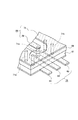
図7は従来のこの種高周波パッケージを示した模式図であり、(a)は側面断面図、(b)は(a)におけるB−B線断面部分の斜視図である。誘電体基板41は厚さTの略直方体板形状に形成されており、誘電体基板41の下面41bにはグランド層42が形成される一方、誘電体基板41の上面41aの所定箇所には、環状の誘電体製の枠体44が形成されている。枠体44の内側領域44dにおける誘電体基板上面41aの所定箇所には、幅がw1 の薄膜状の回路部43aが複数個形成される一方、枠体44を挟んで回路部43aと対向する外側には、これと同様(幅がw1 )のリード部43bがそれぞれ形成されている。回路部43aの一端部とリード部43bの一端部とは幅がw2 の導体部43cを介して接続されており、この導体部43cは枠体44の壁部44a内に埋設されている。これら回路部43a、リード部43b、導体部43cを含んで信号線層43が構成されている。
【0004】
また導体部43cとこの近傍の壁部44aとを含んで構成される回路の特性インピーダンスを、回路部43a、リード部43bのそれと同等にするため、導体部43cの幅w2 は回路部43a及びリード部43bの幅w1 よりも小さい値に設定されている。そして信号線層43における反射損失を抑えて伝送損失を小さくするために、回路部43a、リード部43b、導体部43cにおける各特性インピーダンスの整合が図られている。
【0005】
誘電体基板上面41aにおける枠体内側領域44dの略中央部には半導体素子45が実装されるようになっており、半導体素子45のパッド45aと回路部43aの他端部とはボンディングワイヤ45bを介して接続されるようになっている。枠体44の上面には蓋体46が接合(ハーメチックシール)されるようになっており、この蓋体46により誘電体基板41上の枠体内側領域44dが気密・封止されるようになっている。これら誘電体基板41、グランド層42、信号線層43、枠体44、蓋体46等を含んでマイクロストリップラインタイプの高周波パッケージ40が構成されている。
【0006】
高周波信号(図示せず)は、信号線層43のリード部43bより導体部43c、回路部43a等を介して半導体素子45に入力される一方、半導体素子45より出力された高周波信号は、信号線層43の回路部43a、導体部43c等を介してリード部43bより出力されるようになっている。
しかしながらこのように構成された高周波パッケージ40では、導体部43cの幅w2 が狭くなっており、この寸法精度を確保することが難しく、また抵抗が大きくなり、伝送損失が増大し易い。また製造する際、導体部43cの両端部と壁部44aの内外面44b、44cとを正確に位置合わせすることが難しいという課題があった。
【0007】
この課題に対処するため、信号線層が埋設される枠体部分を薄く形成したものが提案されている。図8は従来のこの種高周波パッケージの主要部を模式的に示した斜視図であり、図中41、42は図7に示したものと同様の誘電体基板、グランド層を示している。誘電体基板41の上面41aの所定箇所には環状をした誘電体製の枠体54が形成され、枠体54の所定箇所には凹部54bが形成されている。一方、誘電体基板41の上面41aの所定箇所には幅がw1 の薄膜状の信号線層53が形成されている。この信号線層53の一端部53a側は枠体54の内側領域54cに形成され、信号線層53の他端部53b側は枠体54の外側領域54dに形成されており、信号線層53の略中央部は凹部54bの近傍内に埋設されている。
【0008】
その他の構成は図7に示したものと略同様であるのでここではその構成の詳細な説明は省略することとする。これら誘電体基板41、グランド層42、信号線層53、枠体54等を含んで高周波パッケージが構成されている。そして高周波信号は、他端部53b側より信号線層53等を介して半導体素子45(図7)に入力される一方、半導体素子45より出力された高周波信号は、信号線層53等を介して他端部53b側より出力されるようになっている。
【0009】
しかしながらこのように構成された高周波パッケージでは、凹部54bの厚さe1 を薄く設定する必要があり、製造が難しく、また凹部54bにおいて強度的に特に弱くなるという課題があった。
また図7、図8に示したマイクロストリップラインタイプの高周波パッケージでは、半導体素子45がミリ波や準ミリ波のようなより高周波数帯域の信号を処理するものである場合、半導体素子45と信号線層43、53との接続損失や、信号線層43、53における放射損失が大きくなり易いという課題があった。
【0010】
この課題に対処するため、近年、誘電体基板の一主面側に信号線層及びグランド層が形成され、これらの上に半導体素子45がフリップチップ実装される、いわゆるコプレナ・ウェーブガイドタイプの高周波パッケージが提案されている。
【0011】
図9は従来のこの種高周波パッケージの要部を示した模式図であり(特開平4−336702号公報)、(a)はパッケージの内部及び外部を示す部分破断平面図、(b)は(a)におけるB−B線断面図、(c)は下面図である。また図10は図9に示した高周波パッケージの要部を示す部分拡大斜視図である。
図中61はセラミック等からなるパッケージ基板を示しており、パッケージ基板61の上面の所定箇所には、環状の誘電体製の枠体62が形成され、枠体62の上面には蓋体63が接合されるようになっている。
【0012】
またパッケージ基板61の上面には、メタライズ65を施したダイボンディング領域64や誘電体基板66が形成されている。誘電体基板66の上面には、金属薄膜からなるパッケージ内部のグランド層78と、所定の線路幅及びグランド層78と所定間隔を有する金属薄膜からなる信号線層79とが形成され、これらグランド層78と信号線層79とを含んで、高周波伝送線路として動作する内部コプレナ線路80が構成されている。
またパッケージ基板61の下面には、グランド層68と信号線層69とが形成され、これらグランド層68と信号線層69とを含んで、外部コプレナ線路70が構成されている。
【0013】
このように図9、図10に示した高周波パッケージにおける内部高周波伝送線路は、信号線層79の両側及び誘電体基板66を挟んで裏側にグランド層78、68が形成された線路構造、いわゆるグランデッド・コプレナ線路構造となっている。
また内部コプレナ線路80を構成する信号線層79、グランド層78と、外部コプレナ線路70を構成する信号線層69、グランド層68とは、金属からなる複数の導体ビア71a、71bを介して接続されている。
【0014】
このように構成された高周波パッケージでは、グランデッド・コプレナ線路構造になっているため、内部側信号線層79の線路幅を半導体素子の線路幅に適合させることができ、パッケージと半導体素子との接続部における高周波的な不整合が解消され、損失を低く抑えること、定在波比(線路を流れる信号の最大電圧と最小電圧との比)を下げることが可能になるとしている。
【0015】
また内部側の信号線層79、グランド層78と、外部側の信号線層69、グランド層68との接続を、複数の導体ビア71a、71bを介して行うため、高周波的な不整合を少なくすることや、アイソレーションを高めることが可能になるとしている。
【0016】
【発明が解決しようとする課題】
高周波特性に優れたパッケージを製造するにあたっては、製造条件が重要になってくる。またこの製造条件については、使用周波数帯域によって変わってくるものであるため、高周波パッケージは使用周波数帯域に合わせた構成にする必要がある。
【0017】
ところが、図9、図10に示した高周波パッケージにおいては、使用周波数帯域を考慮した構成になっておらず、また導体ビア71bの位置や誘電体基板66の厚みについての考慮が何らされていないため、例えば、挿入損失S21については−1.0dB程度に抑えるのが限界であった。
【0018】
本発明は上記課題に鑑みなされたものであって、高周波特性に優れ、かつ伝送特性にも優れた高周波伝送線路基板、及び該高周波伝送線路基板を用いて構成される高周波パッケージを提供することを目的としている。
【0019】
【課題を解決するための手段及びその効果】
上記したように、従来の高周波パッケージにおいては、使用周波数帯域に適したパッケージとすることができなかった。
そこで本発明者は、内部コプレナ線路80と外部コプレナ線路70との距離や、内部側のグランド層78と外部側のグランド層68とを接続するための導体ビア71bと信号線層69、79との距離に着目し、これら距離を調整することによって、使用周波数帯域に適したパッケージを製造することができることを見い出し、本発明を完成するに至った。
【0020】
上記目的を達成するために本発明に係る高周波伝送線路基板(1)は、誘電体基板の一主面側に第1の信号線層と、該第1の信号線層の周囲にギャップを介して形成された第1のグランド層とを備え、前記誘電体基板の他主面側には第2の信号線層と、該第2の信号線層の周囲にギャップを介して形成された第2のグランド層とを備え、前記第1の信号線層の一端部と前記第2の信号線層の一端部とを接続する導体ビア、及び前記第1及び第2の信号線層を挟んで、その両側に前記第1のグランド層と前記第2のグランド層とを接続する複数個の導体ビアが形成された高周波伝送線路基板であって、使用周波数(GHz)をF、前記誘電体基板の比誘電率をεr、前記誘電体基板の厚み(μm)をt、及び前記第1及び第2の信号線層から前記導体ビアまでの距離(μm)をXとするとき、下記数1式を満たす前記各値が、±5%の範囲内で設定されていることを特徴としている。
【0021】
【数1】
F=M0 +M1 t
但し、M0 =a+bX
M1 =c+dX
a=341.2−18.9εr
b=−0.31+0.017εr
c=−0.3+0.02εr
d=0.00031−2.1×10⁻⁵εr
【0022】
上記した高周波伝送線路基板(1)によれば、使用周波数をF、前記誘電体基板の比誘電率をεr 、前記誘電体基板の厚みをt、及び前記第1及び第2の信号線層から前記導体ビアまでの距離をXとするとき、上記数1式を満たす前記各値が、±5%の範囲内で設定されているため、使用周波数Fに適した高周波伝送線路基板とすることができる。従って、高周波特性に優れ、かつ伝送特性にも優れたものとすることができる。
【0023】
また本発明に係る高周波伝送線路基板(2)は、誘電体基板の一主面側に第1の信号線層と、該第1の信号線層の周囲にギャップを介して形成された第1のグランド層とを備え、前記誘電体基板の他主面側には第2の信号線層と、該第2の信号線層の周囲にギャップを介して形成された第2のグランド層とを備え、前記第1の信号線層の一端部と前記第2の信号線層の一端部とを接続する導体ビア、及び前記第1及び第2の信号線層を挟んで、その両側に前記第1のグランド層と前記第2のグランド層とを接続する複数個の導体ビアが形成された高周波伝送線路基板であって、使用周波数(GHz)をFとするとき、前記誘電体基板の比誘電率εr、前記誘電体基板の厚み(μm)t、及び前記第1及び第2の信号線層から前記導体ビアまでの距離(μm)Xが、下記数2式を満たすように設定される値を中心として、±5%の範囲内で設定されていることを特徴としている。
【0024】
【数2】
F+f=M0 +M1 t
但し、M0 =a+bX
M1 =c+dX
a=341.2−18.9εr
b=−0.31+0.017εr
c=−0.3+0.02εr
d=0.00031−2.1×10⁻⁵εr
f:補助周波数。
【0025】
また本発明に係る高周波伝送線路基板(3)は、上記高周波伝送線路基板(2)において、補助周波数fが、−6GHz≦f≦0GHzの範囲内で設定されていることを特徴としている。
【0026】
上記した高周波伝送線路基板(1)のように、上記数1式を満たすように、使用周波数F、前記誘電体基板の比誘電率εr 、前記誘電体基板の厚みt、及び前記第1及び第2の信号線層から前記導体ビアまでの距離Xが設定されただけでは、使用周波数Fに最適なものとすることはできない場合がある。
【0027】
例えば、使用周波数Fを65GHzとし、比誘電率εr を7.7とし、厚みtを300μmとして、数1式より求められた距離Xが640μmとなった場合について説明する。
後述する図1及び図2に示した高周波伝送線路基板において、比誘電率εr が7.7であり、厚みtが300μmの誘電体基板11を用い、信号線層13、16の中心線と各導体ビア19の中心を結ぶ直線との距離Xを640μmとして、シミュレーションを行うと、挿入損失S21の最も良くなる周波数が65GHzではなく、67GHzとなる結果が得られた(図4参照)。すなわち、2GHz程度の誤差があったことになる。
【0028】
このように数1式を満たすように、前記誘電体基板の比誘電率εr 、前記誘電体基板の厚みt、及び前記第1及び第2の信号線層から前記導体ビアまでの距離Xを設定しただけでも、僅か2GHz程度の誤差であるので、使用周波数Fに十分適したものとすることはできるが、最適ではない。
【0029】
上記した高周波伝送線路基板(2)又は(3)によれば、使用周波数をF、前記誘電体基板の比誘電率をεr 、前記誘電体基板の厚みをt、及び前記第1及び第2の信号線層から前記導体ビアまでの距離をXとするとき、前記誤差を考慮に入れた上記数2式を満たす前記各値が、±5%の範囲内で設定されているため、使用周波数Fに最適な高周波伝送線路基板とすることができる。従って、より一層高周波特性に優れ、かつ伝送特性に優れたものとすることができる。
【0030】
また前記誤差については、後述するシミュレーション結果に基づいて、±5GHz程度(図4、図5参照)の範囲内に収まるものと考えられるため、上記した高周波伝送線路基板(3)のように、補助周波数fを、−6GHz≦f≦0GHzの範囲内に設定することができる。
【0031】
従って、F−6≦M 0 +M 1 t≦Fを満たすように、前記誘電体基板の比誘電率εr、前記誘電体基板の厚みt、及び前記第1及び第2の信号線層から前記導体ビアまでの距離Xを設定すれば、使用周波数Fに最適な高周波伝送線路基板を実現することができる。
【0032】
また本発明に係る高周波パッケージは、上記高周波伝送線路基板(1)〜(3)のいずれかを用いて構成されていることを特徴としている。
上記した高周波パッケージによれば、使用周波数Fに適した高周波伝送線路基板を用いて構成されるため、高周波特性に優れ、かつ伝送特性にも優れた高周波パッケージを実現することができる。
【0033】
【発明の実施の形態】
以下、本発明に係る高周波伝送線路基板、及び高周波パッケージの実施の形態を図面に基づいて説明する。
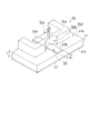
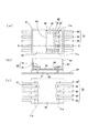
図1は実施の形態(1)に係る高周波伝送線路基板を模式的に示した部分斜視図である。また図2は実施の形態(1)に係る高周波伝送線路基板の主要部を拡大して示した模式図であり、(a)は平面図、(b)は下面図、(c)は(a)におけるC−C線断面図、(d)は(a)におけるD−D線断面図である。
【0034】
誘電体基板11はアルミナセラミック等を用いて厚さがtの略直方体板形状に形成され、誘電体基板11の上面11aの所定箇所には、薄膜状の信号線層13が形成され、信号線層13の周囲にギャップを介してグランド層14が形成され、これらによりコプレナ線路12が構成されている。
【0035】
他方、誘電体基板11の下面11bの所定箇所には、薄膜状の信号線層16が形成され、信号線層16の周囲にギャップを介してグランド層17が形成され、これらによりコプレナ線路15が構成されている。
【0036】
信号線層13の端部13aには導体ビア18の上端部が接続され、導体ビア18の下端部は信号線層16の端部16aに接続されている(図2(c))。また信号線層13、16を挟むその両側には、グランド層14とグランド層17とを接続する導体ビア19が形成されている。
【0037】
また各導体ビア19の中心を結ぶ直線(以下、導体ビア19の中心結線と記す)と信号線層13、16の中心線との距離はXに設定されている。なおこの距離Xは、使用周波数をFとし、誘電体基板11の比誘電率をεr とし、誘電体基板11の厚みをtとした場合に、後述する数3式を満たすように設定される。なお、このとき下記数3式から求められる距離Xの±5%の距離で導体ビア19を設ければ良い。
【0038】
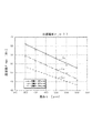
図1及び図2に示した高周波伝送線路基板において、比誘電率εr が7.7の誘電体基板11を用いた場合での挿入損失S21が最も良くなる周波数Fmax と誘電体基板11の厚みtとの関係を図3に示す。図中の直線L1 〜L3 はそれぞれ順に、信号線層13、16の中心線と導体ビア19の中心結線との距離Xを600μm、650μm、700μmとしたものである。
【0039】
本発明者は、図3に示したこれら直線L1 〜L3 を解析することにより、周波数Fmax と、誘電体基板11の比誘電率εr と、誘電体基板の厚みtと、信号線層13、16の中心線と導体ビア19の中心結線との距離Xとの関係を示す下記数3式を導き出した。
【0040】
【数3】
Fmax =M0 +M1 t
但し、M0 =a+bX
M1 =c+dX
a=341.2−18.9εr
b=−0.31+0.017εr
c=−0.3+0.02εr
d=0.00031−2.1×10⁻⁵εr 。
【0041】
上記実施の形態(1)に係る高周波伝送線路基板によれば、使用周波数をF、誘電体基板11の比誘電率をεr 、誘電体基板11の厚みをt、及び信号線層13、16の中心線と導体ビア19の中心結線との距離をXとするとき、上記数3式を満たす前記各値が、±5%の範囲内で設定されているため、使用周波数Fに適した高周波伝送線路基板とすることができる。従って、高周波特性に優れ、かつ伝送特性にも優れたものとすることができる。
【0042】
また、ここでは使用周波数をFとし、誘電体基板11の比誘電率をεr とし、誘電体基板11の厚みをtとして、上記数3式を用いて、信号線層13、16の中心線と導体ビア19の中心結線との距離Xを求めるようにしているが、別の実施の形態では、使用周波数をFとし、誘電体基板11の比誘電率をεr とし、信号線層13、16の中心線と導体ビア19の中心結線との距離をXとして、上記数3式を用いて、誘電体基板11の厚みtを求めるようにしても良く、またこれと同様にして、使用周波数Fや、誘電体基板11の比誘電率εr を求めても良い。
【0043】
また、上記実施の形態に係る高周波伝送線路基板を用いて、高周波パッケージを構成することによって、高周波特性に優れ、かつ伝送特性にも優れた高周波パッケージを実現することができる。
【0044】
【実施例】
以下、実施例に係る高周波伝送線路基板を用い、以下の条件で伝送特性(挿入損失S21)を調査した結果等について説明する。
実施例1、2に係る高周波伝送線路基板の使用周波数F、誘電体基板11の比誘電率εr 、誘電体基板11の厚みtをそれぞれ下記の表1に示した。
【表1】
●実施例1
上記数3式を用いて、以下の条件で信号線層13、16の中心線と導体ビア19の中心結線との距離Xを求めると、距離X≒640μmとなった。
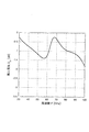
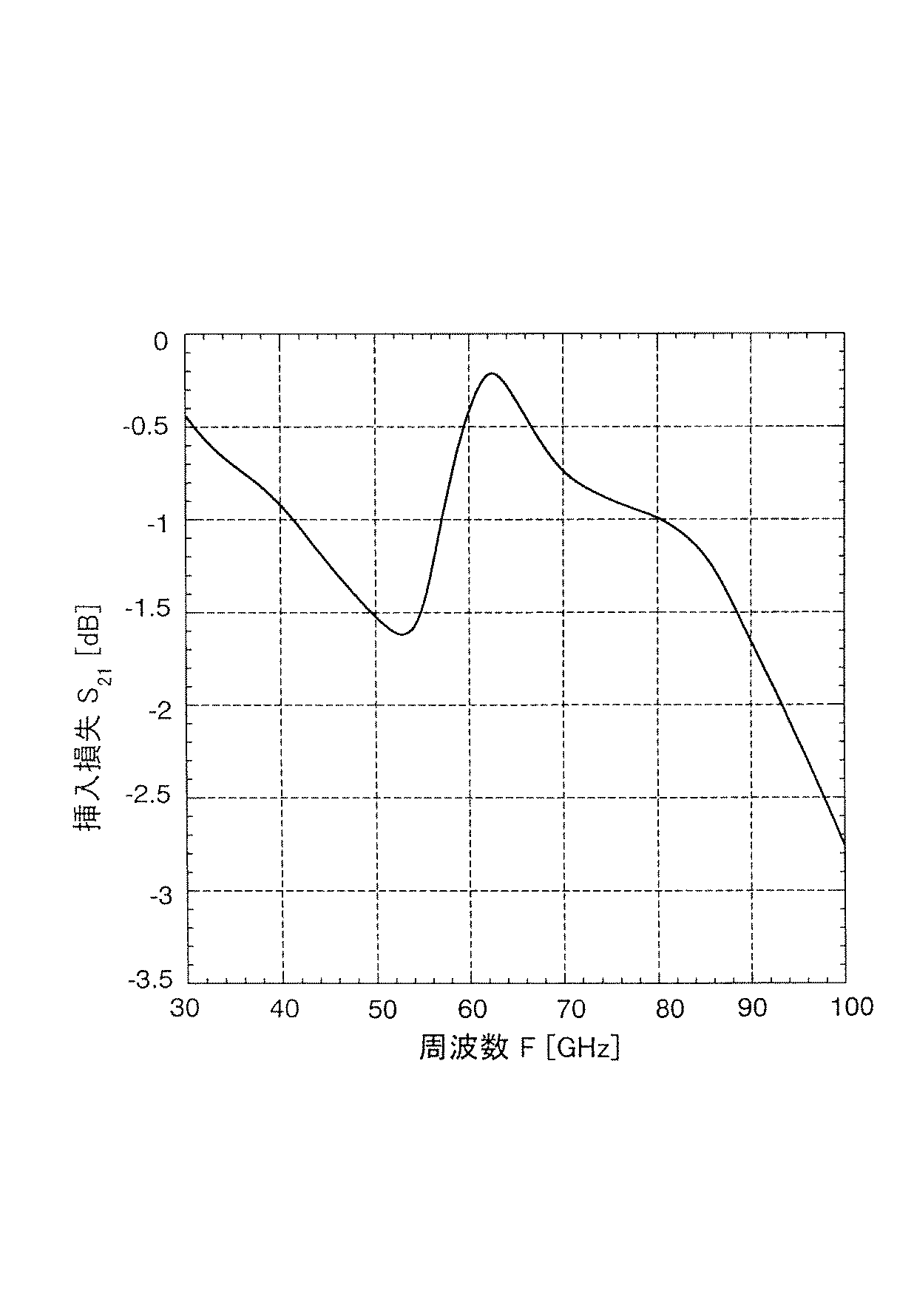
図1及び図2に示した高周波伝送線路基板において、誘電体基板11の比誘電率εr を7.7とし、誘電体基板11の厚みtを300μmとし、信号線層13、16の中心線と導体ビア19の中心結線との距離Xを640μmとしてシミュレーションを行い、解析した結果、図4に示す伝送特性(挿入損失S21)が得られた。図4から明らかなように、使用周波数F(65GHz)において、挿入損失S21が約−0.4dBという優れた伝送特性を有していることが分かる。
【0046】
●実施例2
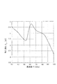
上記数3式を用いて、以下の条件で信号線層13、16の中心線と導体ビア19の中心結線との距離Xを求めると、距離X≒630μmとなった。
図1及び図2に示した高周波伝送線路基板において、誘電体基板11の比誘電率εr を8.9とし、誘電体基板11の厚みtを300μmとし、信号線層13、16の中心線と導体ビア19の中心結線との距離Xを630μmとしてシミュレーションを行い、解析した結果、図5に示す伝送特性(挿入損失S21)が得られた。図5から明らかなように、使用周波数F(60GHz)において、挿入損失S21が約−0.4dBという優れた伝送特性を有していることが分かる。
【0047】
ところで図4から明らかなように、実施例1に係る高周波伝送線路基板において最も適した使用周波数Fは、65GHz(挿入損失S21=−0.4dB)ではなく、67GHz(S21=−0.3dB)であり、また図5から明らかなように、実施例2に係る高周波伝送線路基板において最も適した使用周波数Fは、60GHz(S21=−0.4dB)ではなく、62GHz(S21=−0.2dB)であることが分かる。
換言するならば、図4、図5から使用周波数Fが65GHz、60GHzに最適な高周波伝送線路基板は、実施例1、2に係る高周波伝送線路基板ではないことが分かる。
【0048】
しかしながら、両者共に2GHz程度の僅かな誤差(すなわち、5GHz程度の範囲内に十分収まる僅かな誤差)であるため、実施例1、2に係る高周波伝送線路基板は、使用周波数Fが65GHz、60GHzそれぞれの場合に十分適したものになっていると判断することができる。
【0049】
次に実施例3〜8に係る高周波伝送線路基板の使用周波数F、誘電体基板11の比誘電率εr 、誘電体基板11の厚みtをそれぞれ下記の表2に示した。
【表2】
【0050】
●実施例3〜8
上記数3式を用いて、以下の条件で信号線層13、16の中心線と導体ビア19の中心結線との距離Xを求めると、下記表3に示すようになった。
【表3】
図1及び図2に示した高周波伝送線路基板において、誘電体基板11の比誘電率εr を7.7とし、誘電体基板11の厚みtを300μmとし、信号線層13、16の中心線と導体ビア19の中心結線との距離Xを680、660、650、630、620、600μmとしてシミュレーションを行い、解析した結果、図6に示す伝送特性(挿入損失S21)が得られた。図6から明らかなように、使用周波数F(65GHz)に最も適した高周波伝送線路基板は、実施例5に係る高周波伝送線路基板であることが分かる。
【図面の簡単な説明】
【図1】本発明の実施の形態に係る高周波伝送線路基板を模式的に示した部分斜視図である。
【図2】実施の形態に係る高周波伝送線路基板の主要部を拡大して示した模式図であり、(a)は平面図、(b)は下面図、(c)は(a)におけるC−C線断面図、(d)は(a)におけるD−D線断面図である。
【図3】挿入損失が最も良くなる周波数と誘電体基板の厚みとの関係を示したグラフである。
【図4】実施例1に係る高周波伝送線路基板のシミュレーション結果を示したグラフである。
【図5】実施例2に係る高周波伝送線路基板のシミュレーション結果を示したグラフである。
【図6】実施例5、6、8に係る高周波伝送線路基板のシミュレーション結果を示したグラフである。
【図7】従来の高周波パッケージを示した模式図であり、(a)は側面断面図、(b)は(a)におけるB−B線断面部分の斜視図である。
【図8】従来の別の高周波パッケージの主要部を模式的に示した斜視図である。
【図9】従来のさらに別の高周波パッケージを示した模式図であり、(a)は部分破断平面図、(b)は(a)におけるB−B線断面図、(c)は下面図である。
【図10】図9(a)の要部を模式的に示した部分拡大斜視図である。
【符号の説明】
11 誘電体基板
12、15 コプレナ線路
13、16 信号線層
14、17 グランド層
18、19 導体ビア[0001]
BACKGROUND OF THE INVENTION
The present invention relates to a high-frequency transmission line substrate and a high-frequency package, and more specifically, a high-frequency transmission line substrate on which a semiconductor element using a high-frequency signal is mounted and a high-frequency circuit is formed around the semiconductor element. The present invention relates to a high-frequency package configured by using.
[0002]
[Prior art]
The high-frequency package is configured by hermetically sealing a semiconductor element mounting region formed on a dielectric substrate and a high-frequency circuit in the periphery thereof with an annular frame and a lid bonded to the annular frame, The high frequency signal is input / output through a signal line layer that penetrates the lower surface of the frame.
[0003]
7A and 7B are schematic views showing a conventional high-frequency package of this type, in which FIG. 7A is a side sectional view, and FIG. 7B is a perspective view of a section taken along line BB in FIG. The
[0004]
The characteristic impedance of the circuit configured to include a
[0005]
A
[0006]
A high frequency signal (not shown) is input from the
However, in the high-
[0007]
In order to cope with this problem, a thin frame body in which a signal line layer is embedded has been proposed. FIG. 8 is a perspective view schematically showing the main part of a conventional high-frequency package of this type. In the figure,
[0008]
Since other configurations are substantially the same as those shown in FIG. 7, detailed description of the configurations is omitted here. The
[0009]
However, the high-frequency package configured as described above has a problem in that it is necessary to set the thickness e 1 of the
In the microstrip line type high-frequency package shown in FIGS. 7 and 8, when the
[0010]
In order to cope with this problem, in recent years, a signal line layer and a ground layer are formed on one main surface side of a dielectric substrate, and a
[0011]
FIG. 9 is a schematic view showing the main part of a conventional high frequency package of this type (Japanese Patent Laid-Open No. 4-336702), (a) is a partially broken plan view showing the inside and outside of the package, and (b) is ( A sectional view taken along line BB in a), and (c) is a bottom view. FIG. 10 is a partially enlarged perspective view showing a main part of the high-frequency package shown in FIG.
In the figure,
[0012]
On the upper surface of the
A
[0013]
As described above, the internal high-frequency transmission line in the high-frequency package shown in FIGS. 9 and 10 has a line structure in which
The
[0014]
Since the high-frequency package thus configured has a grounded coplanar line structure, the line width of the internal
[0015]
Further, since the internal
[0016]
[Problems to be solved by the invention]
Manufacturing conditions are important in manufacturing a package with excellent high-frequency characteristics. In addition, since the manufacturing conditions vary depending on the frequency band used, the high frequency package needs to be configured to match the frequency band used.
[0017]
However, the high-frequency package shown in FIGS. 9 and 10 is not configured in consideration of the used frequency band, and the position of the conductor via 71b and the thickness of the
[0018]
The present invention has been made in view of the above problems, and provides a high-frequency transmission line substrate excellent in high-frequency characteristics and excellent in transmission characteristics, and a high-frequency package configured using the high-frequency transmission line substrate. It is aimed.
[0019]
[Means for solving the problems and effects thereof]
As described above, the conventional high-frequency package cannot be a package suitable for the used frequency band.
Therefore, the present inventor has determined the distance between the internal
[0020]
In order to achieve the above object, a high-frequency transmission line substrate (1) according to the present invention includes a first signal line layer on one main surface side of a dielectric substrate, and a gap around the first signal line layer. A first ground layer formed on the other principal surface of the dielectric substrate, and a second signal line layer formed on the periphery of the second signal line layer with a gap interposed therebetween. Two ground layers, with a conductor via connecting one end of the first signal line layer and one end of the second signal line layer, and sandwiching the first and second signal line layers A high-frequency transmission line substrate having a plurality of conductor vias connecting the first ground layer and the second ground layer on both sides thereof, wherein the operating frequency (GHz) is F, and the dielectric substrate Ε r , the dielectric substrate thickness (μm) t, and the first and second signal line layers to When the distance (μm) to the conductor via is X, each value satisfying the
[0021]
[Expression 1]
F = M 0 + M 1 t
However, M 0 = a + bX
M 1 = c + dX
a = 341.2−18.9ε r
b = −0.31 + 0.017ε r
c = −0.3 + 0.02ε r
d = 0.00031−2.1 × 10 −5 ε r
[0022]
According to the above-described high-frequency transmission line substrate (1), the operating frequency is F, the dielectric constant of the dielectric substrate is ε r , the thickness of the dielectric substrate is t, and the first and second signal line layers When the distance from the conductor via to the conductor via is X, each value satisfying the
[0023]
The high-frequency transmission line substrate (2) according to the present invention includes a first signal line layer formed on one principal surface side of the dielectric substrate, and a first signal line layer formed around the first signal line layer with a gap interposed therebetween. A second signal line layer on the other main surface side of the dielectric substrate, and a second ground layer formed around the second signal line layer with a gap interposed therebetween. A conductor via that connects one end of the first signal line layer and one end of the second signal line layer, and the first and second signal line layers sandwiched between the first signal line layer and the first signal line layer. A high-frequency transmission line substrate in which a plurality of conductor vias that connect one ground layer and the second ground layer are formed, and when the operating frequency (GHz) is F, the dielectric constant of the dielectric substrate rate epsilon r, the dielectric thickness of the substrate (μm) t, and from the first and second signal line to said conductive vias Distance ([mu] m) X is, around the value set so as to satisfy the
[0024]
[Expression 2]
F + f = M 0 + M 1 t
However, M 0 = a + bX
M 1 = c + dX
a = 341.2−18.9ε r
b = −0.31 + 0.017ε r
c = −0.3 + 0.02ε r
d = 0.00031−2.1 × 10 −5 ε r
f: Auxiliary frequency.
[0025]
The high-frequency transmission line substrate (3) according to the present invention is characterized in that, in the high-frequency transmission line substrate (2), the auxiliary frequency f is set within a range of −6 GHz ≦ f ≦ 0 GHz .
[0026]
As in the high-frequency transmission line substrate (1), the operating frequency F, the relative permittivity ε r of the dielectric substrate, the thickness t of the dielectric substrate, and the first and It may not be possible to optimize the operating frequency F only by setting the distance X from the second signal line layer to the conductor via.
[0027]
For example, a case will be described in which the operating frequency F is 65 GHz, the relative dielectric constant ε r is 7.7, the thickness t is 300 μm, and the distance X obtained from
In the high-frequency transmission line substrate shown in FIGS. 1 and 2 to be described later, a
[0028]
In this way, the relative permittivity ε r of the dielectric substrate, the thickness t of the dielectric substrate, and the distance X from the first and second signal line layers to the conductor via are set so as to satisfy Equation (1). Even if it is set, it is an error of only about 2 GHz, so that it can be made sufficiently suitable for the operating frequency F, but it is not optimal.
[0029]
According to the high frequency transmission line substrate (2) or (3) described above, the operating frequency is F, the relative permittivity of the dielectric substrate is ε r , the thickness of the dielectric substrate is t, and the first and second When the distance from the signal line layer to the conductor via is X, the values satisfying the
[0030]
Further, since the error is considered to be within a range of about ± 5 GHz (see FIGS. 4 and 5) based on a simulation result to be described later, as in the high-frequency transmission line substrate (3) described above, an auxiliary is provided. The frequency f can be set within a range of −6 GHz ≦ f ≦ 0 GHz .
[0031]
Therefore, from the relative permittivity ε r of the dielectric substrate, the thickness t of the dielectric substrate, and the first and second signal line layers so as to satisfy F−6 ≦ M 0 + M 1 t ≦ F. If the distance X to the conductor via is set, a high-frequency transmission line substrate optimal for the operating frequency F can be realized.
[0032]
The high-frequency package according to the present invention is characterized by being configured using any one of the high-frequency transmission line substrates (1) to (3).
According to the above-described high frequency package, since the high frequency transmission line substrate suitable for the operating frequency F is used, a high frequency package having excellent high frequency characteristics and excellent transmission characteristics can be realized.
[0033]
DETAILED DESCRIPTION OF THE INVENTION
Embodiments of a high-frequency transmission line substrate and a high-frequency package according to the present invention will be described below with reference to the drawings.
FIG. 1 is a partial perspective view schematically showing a high-frequency transmission line substrate according to Embodiment (1). FIG. 2 is an enlarged schematic view showing the main part of the high-frequency transmission line substrate according to the embodiment (1), where (a) is a plan view, (b) is a bottom view, and (c) is (a). ) Is a cross-sectional view taken along the line CC in FIG. 5, and FIG. 4D is a cross-sectional view taken along the line DD in FIG.
[0034]
The
[0035]
On the other hand, a thin
[0036]
The upper end portion of the conductor via 18 is connected to the
[0037]
The distance between the straight line connecting the centers of the conductor vias 19 (hereinafter referred to as the center connection of the conductor vias 19) and the center lines of the signal line layers 13 and 16 is set to X. The distance X is set so as to satisfy the following formula (3) when the operating frequency is F, the relative dielectric constant of the
[0038]
In the high-frequency transmission line substrate shown in FIGS. 1 and 2, the frequency F max and the
[0039]
By analyzing these straight lines L 1 to L 3 shown in FIG. 3, the inventor analyzed the frequency F max , the relative dielectric constant ε r of the
[0040]
[Equation 3]
F max = M 0 + M 1 t
However, M 0 = a + bX
M 1 = c + dX
a = 341.2−18.9ε r
b = −0.31 + 0.017ε r
c = −0.3 + 0.02ε r
d = 0.00031−2.1 × 10 −5 ε r .
[0041]
According to the high frequency transmission line substrate according to the embodiment (1), the operating frequency is F, the relative dielectric constant of the
[0042]
Further, here, the frequency used is F, the relative dielectric constant of the
[0043]
Further, by configuring a high frequency package using the high frequency transmission line substrate according to the above embodiment, a high frequency package having excellent high frequency characteristics and excellent transmission characteristics can be realized.
[0044]
【Example】
Hereinafter, the results of examining the transmission characteristics (insertion loss S 21 ) under the following conditions using the high-frequency transmission line substrate according to the example will be described.
The operating frequency F of the high-frequency transmission line substrate according to Examples 1 and 2, the relative permittivity ε r of the
[Table 1]
Example 1
Using the
In the high-frequency transmission line substrate shown in FIGS. 1 and 2, the relative permittivity ε r of the
[0046]
Example 2
Using the
In the high-frequency transmission line substrate shown in FIGS. 1 and 2, the
[0047]
As is apparent from FIG. 4, the most suitable operating frequency F in the high-frequency transmission line substrate according to the first embodiment is not 65 GHz (insertion loss S 21 = −0.4 dB), but 67 GHz (S 21 = −0. As is clear from FIG. 5, the most suitable operating frequency F in the high-frequency transmission line substrate according to Example 2 is not 60 GHz (S 21 = −0.4 dB), but 62 GHz (S 21 = -0.2 dB).
In other words, it can be seen from FIGS. 4 and 5 that the optimum high-frequency transmission line substrate for the operating frequencies F of 65 GHz and 60 GHz is not the high-frequency transmission line substrate according to Examples 1 and 2.
[0048]
However, since both are slight errors of about 2 GHz (that is, small errors that are well within the range of about 5 GHz), the high-frequency transmission line substrates according to the first and second embodiments use frequencies F of 65 GHz and 60 GHz, respectively. In this case, it can be determined that it is sufficiently suitable.
[0049]
Next, Table 2 shows the operating frequency F of the high-frequency transmission line substrate according to Examples 3 to 8, the relative dielectric constant ε r of the
[Table 2]
[0050]
Examples 3 to 8
Using the
[Table 3]
In the high-frequency transmission line substrate shown in FIGS. 1 and 2, the relative permittivity ε r of the
[Brief description of the drawings]
FIG. 1 is a partial perspective view schematically showing a high-frequency transmission line substrate according to an embodiment of the present invention.
2A and 2B are schematic views showing an enlarged main part of the high-frequency transmission line substrate according to the embodiment, where FIG. 2A is a plan view, FIG. 2B is a bottom view, and FIG. -C line sectional drawing, (d) is the DD line sectional drawing in (a).
FIG. 3 is a graph showing the relationship between the frequency at which the insertion loss is the best and the thickness of the dielectric substrate.
4 is a graph showing simulation results of the high-frequency transmission line substrate according to Example 1. FIG.
5 is a graph showing simulation results of the high-frequency transmission line substrate according to Example 2. FIG.
6 is a graph showing simulation results of high-frequency transmission line substrates according to Examples 5, 6, and 8. FIG.
7A and 7B are schematic views showing a conventional high-frequency package, where FIG. 7A is a side cross-sectional view, and FIG. 7B is a perspective view of a cross-sectional portion taken along line BB in FIG.
FIG. 8 is a perspective view schematically showing a main part of another conventional high-frequency package.
9A and 9B are schematic views showing still another conventional high-frequency package, where FIG. 9A is a partially broken plan view, FIG. 9B is a sectional view taken along line BB in FIG. 9A, and FIG. is there.
10 is a partially enlarged perspective view schematically showing the main part of FIG. 9 (a). FIG.
[Explanation of symbols]
11
Claims (4)
前記誘電体基板の他主面側には第2の信号線層と、該第2の信号線層の周囲にギャップを介して形成された第2のグランド層とを備え、
前記第1の信号線層の一端部と前記第2の信号線層の一端部とを接続する導体ビア、及び前記第1及び第2の信号線層を挟んで、その両側に前記第1のグランド層と前記第2のグランド層とを接続する複数個の導体ビアが形成された高周波伝送線路基板であって、
使用周波数(GHz)をF、前記誘電体基板の比誘電率をεr、前記誘電体基板の厚み(μm)をt、及び前記第1及び第2の信号線層から前記導体ビアまでの距離(μm)をXとするとき、
F=M0 +M1 t
但し、M0 =a+bX
M1 =c+dX
a=341.2−18.9εr
b=−0.31+0.017εr
c=−0.3+0.02εr
d=0.00031−2.1×10⁻⁵εr
の関係を満たす前記各値が、±5%の範囲内で設定されていることを特徴とする高周波伝送線路基板。A first signal line layer on one main surface side of the dielectric substrate, and a first ground layer formed around the first signal line layer with a gap therebetween,
The other main surface side of the dielectric substrate includes a second signal line layer and a second ground layer formed around the second signal line layer with a gap interposed therebetween,
Conductive vias connecting one end of the first signal line layer and one end of the second signal line layer, and the first and second signal line layers sandwiched between the first signal line layer and the first signal line layer. A high-frequency transmission line substrate having a plurality of conductive vias connecting a ground layer and the second ground layer,
The operating frequency (GHz) is F, the relative permittivity of the dielectric substrate is ε r , the thickness (μm) of the dielectric substrate is t, and the distance from the first and second signal line layers to the conductor vias When (μm) is X,
F = M 0 + M 1 t
However, M 0 = a + bX
M 1 = c + dX
a = 341.2−18.9ε r
b = −0.31 + 0.017ε r
c = −0.3 + 0.02ε r
d = 0.00031−2.1 × 10 −5 ε r
Each of the values satisfying the relationship is set within a range of ± 5%.
前記誘電体基板の他主面側には第2の信号線層と、該第2の信号線層の周囲にギャップを介して形成された第2のグランド層とを備え、
前記第1の信号線層の一端部と前記第2の信号線層の一端部とを接続する導体ビア、及び前記第1及び第2の信号線層を挟んで、その両側に前記第1のグランド層と前記第2のグランド層とを接続する複数個の導体ビアが形成された高周波伝送線路基板であって、
使用周波数(GHz)をF、前記誘電体基板の比誘電率をεr、前記誘電体基板の厚み(μm)をt、及び前記第1及び第2の信号線層から前記導体ビアまでの距離(μm)をXとするとき、
F+f=M0 +M1 t
但し、M0 =a+bX
M1 =c+dX
a=341.2−18.9εr
b=−0.31+0.017εr
c=−0.3+0.02εr
d=0.00031−2.1×10⁻⁵εr
f:補助周波数
の関係を満たす前記各値が、±5%の範囲内で設定されていることを特徴とする高周波伝送線路基板。A first signal line layer on one main surface side of the dielectric substrate, and a first ground layer formed around the first signal line layer with a gap therebetween,
The other main surface side of the dielectric substrate includes a second signal line layer and a second ground layer formed around the second signal line layer with a gap interposed therebetween,
Conductive vias connecting one end of the first signal line layer and one end of the second signal line layer, and the first and second signal line layers sandwiched between the first signal line layer and the first signal line layer. A high-frequency transmission line substrate having a plurality of conductive vias connecting a ground layer and the second ground layer,
The operating frequency (GHz) is F, the relative permittivity of the dielectric substrate is ε r , the thickness (μm) of the dielectric substrate is t, and the distance from the first and second signal line layers to the conductor vias When (μm) is X,
F + f = M 0 + M 1 t
However, M 0 = a + bX
M 1 = c + dX
a = 341.2−18.9ε r
b = −0.31 + 0.017ε r
c = −0.3 + 0.02ε r
d = 0.00031−2.1 × 10 −5 ε r
f: Each value satisfying the relationship of the auxiliary frequency is set within a range of ± 5%.
Priority Applications (1)
| Application Number | Priority Date | Filing Date | Title |
|---|---|---|---|
| JP2000113659A JP4018317B2 (en) | 2000-04-14 | 2000-04-14 | High frequency transmission line substrate and high frequency package |
Applications Claiming Priority (1)
| Application Number | Priority Date | Filing Date | Title |
|---|---|---|---|
| JP2000113659A JP4018317B2 (en) | 2000-04-14 | 2000-04-14 | High frequency transmission line substrate and high frequency package |
Publications (2)
| Publication Number | Publication Date |
|---|---|
| JP2001298306A JP2001298306A (en) | 2001-10-26 |
| JP4018317B2 true JP4018317B2 (en) | 2007-12-05 |
Family
ID=18625585
Family Applications (1)
| Application Number | Title | Priority Date | Filing Date |
|---|---|---|---|
| JP2000113659A Expired - Lifetime JP4018317B2 (en) | 2000-04-14 | 2000-04-14 | High frequency transmission line substrate and high frequency package |
Country Status (1)
| Country | Link |
|---|---|
| JP (1) | JP4018317B2 (en) |
Families Citing this family (5)
| Publication number | Priority date | Publication date | Assignee | Title |
|---|---|---|---|---|
| US6891266B2 (en) * | 2002-02-14 | 2005-05-10 | Mia-Com | RF transition for an area array package |
| US20100254094A1 (en) * | 2007-10-25 | 2010-10-07 | Risato Ohhira | High-Frequency Wiring Board and High-Frequency Module That Uses the High-Frequency Wiring Board |
| JP5737476B2 (en) | 2012-06-29 | 2015-06-17 | 株式会社村田製作所 | High frequency signal line |
| CN204271225U (en) | 2012-06-29 | 2015-04-15 | 株式会社村田制作所 | High-frequency signal circuit |
| CN113873740B (en) * | 2020-06-30 | 2026-01-02 | 昆山展腾电子科技有限公司 | Transmission line structure |
-
2000
- 2000-04-14 JP JP2000113659A patent/JP4018317B2/en not_active Expired - Lifetime
Also Published As
| Publication number | Publication date |
|---|---|
| JP2001298306A (en) | 2001-10-26 |
Similar Documents
| Publication | Publication Date | Title |
|---|---|---|
| KR100430299B1 (en) | Radio frequency circuit module on multi-layer substrate | |
| US6674347B1 (en) | Multi-layer substrate suppressing an unwanted transmission mode | |
| US10777493B2 (en) | Semiconductor device mounting board and semiconductor package | |
| JP4081284B2 (en) | High frequency integrated circuit module | |
| JP3493301B2 (en) | High frequency input / output terminals and high frequency semiconductor element storage package | |
| JP4018317B2 (en) | High frequency transmission line substrate and high frequency package | |
| US6781488B2 (en) | Connected construction of a high-frequency package and a wiring board | |
| US20230189429A1 (en) | Module | |
| JP4012796B2 (en) | Laminated structure for high-frequency signal transmission and high-frequency semiconductor package using the same | |
| JP4042338B2 (en) | Flip chip mounting board | |
| JP2003152124A (en) | High frequency package | |
| JP2002185201A (en) | High frequency wiring board | |
| JP3618046B2 (en) | High frequency circuit package | |
| JP3810566B2 (en) | High frequency package | |
| JP3996330B2 (en) | High frequency package | |
| JP2002190541A (en) | High frequency circuit package | |
| JP4009217B2 (en) | Laminated structure for high-frequency signal transmission and high-frequency semiconductor package using the same | |
| JP2002359443A (en) | Connection structure between high-frequency package and wiring board | |
| JP2002299502A (en) | Package for storing high-frequency semiconductor elements | |
| JP3833426B2 (en) | High frequency wiring board | |
| JP3939059B2 (en) | High frequency package | |
| JP2000183230A (en) | Mounting structure of high frequency circuit package | |
| JPH08274248A (en) | Ultra-wide band integrated circuit device | |
| JP3987659B2 (en) | High frequency semiconductor device | |
| JP2000286364A (en) | High frequency package |
Legal Events
| Date | Code | Title | Description |
|---|---|---|---|
| A621 | Written request for application examination |
Free format text: JAPANESE INTERMEDIATE CODE: A621 Effective date: 20050106 |
|
| A977 | Report on retrieval |
Free format text: JAPANESE INTERMEDIATE CODE: A971007 Effective date: 20060927 |
|
| A131 | Notification of reasons for refusal |
Free format text: JAPANESE INTERMEDIATE CODE: A131 Effective date: 20061005 |
|
| A521 | Written amendment |
Free format text: JAPANESE INTERMEDIATE CODE: A523 Effective date: 20061204 |
|
| A131 | Notification of reasons for refusal |
Free format text: JAPANESE INTERMEDIATE CODE: A131 Effective date: 20070403 |
|
| A521 | Written amendment |
Free format text: JAPANESE INTERMEDIATE CODE: A523 Effective date: 20070524 |
|
| TRDD | Decision of grant or rejection written | ||
| A01 | Written decision to grant a patent or to grant a registration (utility model) |
Free format text: JAPANESE INTERMEDIATE CODE: A01 Effective date: 20070911 |
|
| A61 | First payment of annual fees (during grant procedure) |
Free format text: JAPANESE INTERMEDIATE CODE: A61 Effective date: 20070920 |
|
| R150 | Certificate of patent or registration of utility model |
Free format text: JAPANESE INTERMEDIATE CODE: R150 Ref document number: 4018317 Country of ref document: JP Free format text: JAPANESE INTERMEDIATE CODE: R150 |
|
| FPAY | Renewal fee payment (event date is renewal date of database) |
Free format text: PAYMENT UNTIL: 20100928 Year of fee payment: 3 |
|
| FPAY | Renewal fee payment (event date is renewal date of database) |
Free format text: PAYMENT UNTIL: 20100928 Year of fee payment: 3 |
|
| FPAY | Renewal fee payment (event date is renewal date of database) |
Free format text: PAYMENT UNTIL: 20110928 Year of fee payment: 4 |
|
| R250 | Receipt of annual fees |
Free format text: JAPANESE INTERMEDIATE CODE: R250 |
|
| FPAY | Renewal fee payment (event date is renewal date of database) |
Free format text: PAYMENT UNTIL: 20120928 Year of fee payment: 5 |
|
| R250 | Receipt of annual fees |
Free format text: JAPANESE INTERMEDIATE CODE: R250 |
|
| FPAY | Renewal fee payment (event date is renewal date of database) |
Free format text: PAYMENT UNTIL: 20130928 Year of fee payment: 6 |
|
| R250 | Receipt of annual fees |
Free format text: JAPANESE INTERMEDIATE CODE: R250 |
|
| S533 | Written request for registration of change of name |
Free format text: JAPANESE INTERMEDIATE CODE: R313533 |
|
| FPAY | Renewal fee payment (event date is renewal date of database) |
Free format text: PAYMENT UNTIL: 20130928 Year of fee payment: 6 |
|
| R350 | Written notification of registration of transfer |
Free format text: JAPANESE INTERMEDIATE CODE: R350 |
|
| R250 | Receipt of annual fees |
Free format text: JAPANESE INTERMEDIATE CODE: R250 |
|
| R250 | Receipt of annual fees |
Free format text: JAPANESE INTERMEDIATE CODE: R250 |
|
| R250 | Receipt of annual fees |
Free format text: JAPANESE INTERMEDIATE CODE: R250 |
|
| R250 | Receipt of annual fees |
Free format text: JAPANESE INTERMEDIATE CODE: R250 |
|
| R250 | Receipt of annual fees |
Free format text: JAPANESE INTERMEDIATE CODE: R250 |
|
| R250 | Receipt of annual fees |
Free format text: JAPANESE INTERMEDIATE CODE: R250 |
|
| R250 | Receipt of annual fees |
Free format text: JAPANESE INTERMEDIATE CODE: R250 |
|
| EXPY | Cancellation because of completion of term |