JP4012411B2 - Semiconductor device and manufacturing method thereof - Google Patents
Semiconductor device and manufacturing method thereof Download PDFInfo
- Publication number
- JP4012411B2 JP4012411B2 JP2002036129A JP2002036129A JP4012411B2 JP 4012411 B2 JP4012411 B2 JP 4012411B2 JP 2002036129 A JP2002036129 A JP 2002036129A JP 2002036129 A JP2002036129 A JP 2002036129A JP 4012411 B2 JP4012411 B2 JP 4012411B2
- Authority
- JP
- Japan
- Prior art keywords
- film
- semiconductor device
- electrode
- pentoxide
- niobium pentoxide
- Prior art date
- Legal status (The legal status is an assumption and is not a legal conclusion. Google has not performed a legal analysis and makes no representation as to the accuracy of the status listed.)
- Expired - Fee Related
Links
Images


Classifications
-
- H—ELECTRICITY
- H01—ELECTRIC ELEMENTS
- H01L—SEMICONDUCTOR DEVICES NOT COVERED BY CLASS H10
- H01L21/00—Processes or apparatus adapted for the manufacture or treatment of semiconductor or solid state devices or of parts thereof
- H01L21/02—Manufacture or treatment of semiconductor devices or of parts thereof
- H01L21/02104—Forming layers
- H01L21/02107—Forming insulating materials on a substrate
- H01L21/02109—Forming insulating materials on a substrate characterised by the type of layer, e.g. type of material, porous/non-porous, pre-cursors, mixtures or laminates
- H01L21/022—Forming insulating materials on a substrate characterised by the type of layer, e.g. type of material, porous/non-porous, pre-cursors, mixtures or laminates the layer being a laminate, i.e. composed of sublayers, e.g. stacks of alternating high-k metal oxides
-
- C—CHEMISTRY; METALLURGY
- C23—COATING METALLIC MATERIAL; COATING MATERIAL WITH METALLIC MATERIAL; CHEMICAL SURFACE TREATMENT; DIFFUSION TREATMENT OF METALLIC MATERIAL; COATING BY VACUUM EVAPORATION, BY SPUTTERING, BY ION IMPLANTATION OR BY CHEMICAL VAPOUR DEPOSITION, IN GENERAL; INHIBITING CORROSION OF METALLIC MATERIAL OR INCRUSTATION IN GENERAL
- C23C—COATING METALLIC MATERIAL; COATING MATERIAL WITH METALLIC MATERIAL; SURFACE TREATMENT OF METALLIC MATERIAL BY DIFFUSION INTO THE SURFACE, BY CHEMICAL CONVERSION OR SUBSTITUTION; COATING BY VACUUM EVAPORATION, BY SPUTTERING, BY ION IMPLANTATION OR BY CHEMICAL VAPOUR DEPOSITION, IN GENERAL
- C23C16/00—Chemical coating by decomposition of gaseous compounds, without leaving reaction products of surface material in the coating, i.e. chemical vapour deposition [CVD] processes
- C23C16/06—Chemical coating by decomposition of gaseous compounds, without leaving reaction products of surface material in the coating, i.e. chemical vapour deposition [CVD] processes characterised by the deposition of metallic material
- C23C16/18—Chemical coating by decomposition of gaseous compounds, without leaving reaction products of surface material in the coating, i.e. chemical vapour deposition [CVD] processes characterised by the deposition of metallic material from metallo-organic compounds
-
- C—CHEMISTRY; METALLURGY
- C23—COATING METALLIC MATERIAL; COATING MATERIAL WITH METALLIC MATERIAL; CHEMICAL SURFACE TREATMENT; DIFFUSION TREATMENT OF METALLIC MATERIAL; COATING BY VACUUM EVAPORATION, BY SPUTTERING, BY ION IMPLANTATION OR BY CHEMICAL VAPOUR DEPOSITION, IN GENERAL; INHIBITING CORROSION OF METALLIC MATERIAL OR INCRUSTATION IN GENERAL
- C23C—COATING METALLIC MATERIAL; COATING MATERIAL WITH METALLIC MATERIAL; SURFACE TREATMENT OF METALLIC MATERIAL BY DIFFUSION INTO THE SURFACE, BY CHEMICAL CONVERSION OR SUBSTITUTION; COATING BY VACUUM EVAPORATION, BY SPUTTERING, BY ION IMPLANTATION OR BY CHEMICAL VAPOUR DEPOSITION, IN GENERAL
- C23C16/00—Chemical coating by decomposition of gaseous compounds, without leaving reaction products of surface material in the coating, i.e. chemical vapour deposition [CVD] processes
- C23C16/22—Chemical coating by decomposition of gaseous compounds, without leaving reaction products of surface material in the coating, i.e. chemical vapour deposition [CVD] processes characterised by the deposition of inorganic material, other than metallic material
- C23C16/30—Deposition of compounds, mixtures or solid solutions, e.g. borides, carbides, nitrides
- C23C16/40—Oxides
- C23C16/405—Oxides of refractory metals or yttrium
-
- C—CHEMISTRY; METALLURGY
- C23—COATING METALLIC MATERIAL; COATING MATERIAL WITH METALLIC MATERIAL; CHEMICAL SURFACE TREATMENT; DIFFUSION TREATMENT OF METALLIC MATERIAL; COATING BY VACUUM EVAPORATION, BY SPUTTERING, BY ION IMPLANTATION OR BY CHEMICAL VAPOUR DEPOSITION, IN GENERAL; INHIBITING CORROSION OF METALLIC MATERIAL OR INCRUSTATION IN GENERAL
- C23C—COATING METALLIC MATERIAL; COATING MATERIAL WITH METALLIC MATERIAL; SURFACE TREATMENT OF METALLIC MATERIAL BY DIFFUSION INTO THE SURFACE, BY CHEMICAL CONVERSION OR SUBSTITUTION; COATING BY VACUUM EVAPORATION, BY SPUTTERING, BY ION IMPLANTATION OR BY CHEMICAL VAPOUR DEPOSITION, IN GENERAL
- C23C16/00—Chemical coating by decomposition of gaseous compounds, without leaving reaction products of surface material in the coating, i.e. chemical vapour deposition [CVD] processes
- C23C16/56—After-treatment
-
- H—ELECTRICITY
- H01—ELECTRIC ELEMENTS
- H01L—SEMICONDUCTOR DEVICES NOT COVERED BY CLASS H10
- H01L21/00—Processes or apparatus adapted for the manufacture or treatment of semiconductor or solid state devices or of parts thereof
- H01L21/02—Manufacture or treatment of semiconductor devices or of parts thereof
- H01L21/02104—Forming layers
- H01L21/02107—Forming insulating materials on a substrate
- H01L21/02109—Forming insulating materials on a substrate characterised by the type of layer, e.g. type of material, porous/non-porous, pre-cursors, mixtures or laminates
- H01L21/02112—Forming insulating materials on a substrate characterised by the type of layer, e.g. type of material, porous/non-porous, pre-cursors, mixtures or laminates characterised by the material of the layer
- H01L21/02172—Forming insulating materials on a substrate characterised by the type of layer, e.g. type of material, porous/non-porous, pre-cursors, mixtures or laminates characterised by the material of the layer the material containing at least one metal element, e.g. metal oxides, metal nitrides, metal oxynitrides or metal carbides
- H01L21/02175—Forming insulating materials on a substrate characterised by the type of layer, e.g. type of material, porous/non-porous, pre-cursors, mixtures or laminates characterised by the material of the layer the material containing at least one metal element, e.g. metal oxides, metal nitrides, metal oxynitrides or metal carbides characterised by the metal
- H01L21/02183—Forming insulating materials on a substrate characterised by the type of layer, e.g. type of material, porous/non-porous, pre-cursors, mixtures or laminates characterised by the material of the layer the material containing at least one metal element, e.g. metal oxides, metal nitrides, metal oxynitrides or metal carbides characterised by the metal the material containing tantalum, e.g. Ta2O5
-
- H—ELECTRICITY
- H01—ELECTRIC ELEMENTS
- H01L—SEMICONDUCTOR DEVICES NOT COVERED BY CLASS H10
- H01L21/00—Processes or apparatus adapted for the manufacture or treatment of semiconductor or solid state devices or of parts thereof
- H01L21/02—Manufacture or treatment of semiconductor devices or of parts thereof
- H01L21/02104—Forming layers
- H01L21/02107—Forming insulating materials on a substrate
- H01L21/02109—Forming insulating materials on a substrate characterised by the type of layer, e.g. type of material, porous/non-porous, pre-cursors, mixtures or laminates
- H01L21/02112—Forming insulating materials on a substrate characterised by the type of layer, e.g. type of material, porous/non-porous, pre-cursors, mixtures or laminates characterised by the material of the layer
- H01L21/02172—Forming insulating materials on a substrate characterised by the type of layer, e.g. type of material, porous/non-porous, pre-cursors, mixtures or laminates characterised by the material of the layer the material containing at least one metal element, e.g. metal oxides, metal nitrides, metal oxynitrides or metal carbides
- H01L21/02175—Forming insulating materials on a substrate characterised by the type of layer, e.g. type of material, porous/non-porous, pre-cursors, mixtures or laminates characterised by the material of the layer the material containing at least one metal element, e.g. metal oxides, metal nitrides, metal oxynitrides or metal carbides characterised by the metal
- H01L21/02194—Forming insulating materials on a substrate characterised by the type of layer, e.g. type of material, porous/non-porous, pre-cursors, mixtures or laminates characterised by the material of the layer the material containing at least one metal element, e.g. metal oxides, metal nitrides, metal oxynitrides or metal carbides characterised by the metal the material containing more than one metal element
-
- H—ELECTRICITY
- H01—ELECTRIC ELEMENTS
- H01L—SEMICONDUCTOR DEVICES NOT COVERED BY CLASS H10
- H01L21/00—Processes or apparatus adapted for the manufacture or treatment of semiconductor or solid state devices or of parts thereof
- H01L21/02—Manufacture or treatment of semiconductor devices or of parts thereof
- H01L21/02104—Forming layers
- H01L21/02107—Forming insulating materials on a substrate
- H01L21/02225—Forming insulating materials on a substrate characterised by the process for the formation of the insulating layer
- H01L21/0226—Forming insulating materials on a substrate characterised by the process for the formation of the insulating layer formation by a deposition process
- H01L21/02263—Forming insulating materials on a substrate characterised by the process for the formation of the insulating layer formation by a deposition process deposition from the gas or vapour phase
- H01L21/02271—Forming insulating materials on a substrate characterised by the process for the formation of the insulating layer formation by a deposition process deposition from the gas or vapour phase deposition by decomposition or reaction of gaseous or vapour phase compounds, i.e. chemical vapour deposition
-
- H—ELECTRICITY
- H01—ELECTRIC ELEMENTS
- H01L—SEMICONDUCTOR DEVICES NOT COVERED BY CLASS H10
- H01L21/00—Processes or apparatus adapted for the manufacture or treatment of semiconductor or solid state devices or of parts thereof
- H01L21/02—Manufacture or treatment of semiconductor devices or of parts thereof
- H01L21/02104—Forming layers
- H01L21/02107—Forming insulating materials on a substrate
- H01L21/02296—Forming insulating materials on a substrate characterised by the treatment performed before or after the formation of the layer
- H01L21/02318—Forming insulating materials on a substrate characterised by the treatment performed before or after the formation of the layer post-treatment
- H01L21/02356—Forming insulating materials on a substrate characterised by the treatment performed before or after the formation of the layer post-treatment treatment to change the morphology of the insulating layer, e.g. transformation of an amorphous layer into a crystalline layer
-
- H—ELECTRICITY
- H01—ELECTRIC ELEMENTS
- H01L—SEMICONDUCTOR DEVICES NOT COVERED BY CLASS H10
- H01L21/00—Processes or apparatus adapted for the manufacture or treatment of semiconductor or solid state devices or of parts thereof
- H01L21/02—Manufacture or treatment of semiconductor devices or of parts thereof
- H01L21/04—Manufacture or treatment of semiconductor devices or of parts thereof the devices having at least one potential-jump barrier or surface barrier, e.g. PN junction, depletion layer or carrier concentration layer
- H01L21/18—Manufacture or treatment of semiconductor devices or of parts thereof the devices having at least one potential-jump barrier or surface barrier, e.g. PN junction, depletion layer or carrier concentration layer the devices having semiconductor bodies comprising elements of Group IV of the Periodic System or AIIIBV compounds with or without impurities, e.g. doping materials
- H01L21/30—Treatment of semiconductor bodies using processes or apparatus not provided for in groups H01L21/20 - H01L21/26
- H01L21/31—Treatment of semiconductor bodies using processes or apparatus not provided for in groups H01L21/20 - H01L21/26 to form insulating layers thereon, e.g. for masking or by using photolithographic techniques; After treatment of these layers; Selection of materials for these layers
- H01L21/314—Inorganic layers
- H01L21/316—Inorganic layers composed of oxides or glassy oxides or oxide based glass
- H01L21/31604—Deposition from a gas or vapour
- H01L21/31637—Deposition of Tantalum oxides, e.g. Ta2O5
-
- H—ELECTRICITY
- H01—ELECTRIC ELEMENTS
- H01L—SEMICONDUCTOR DEVICES NOT COVERED BY CLASS H10
- H01L28/00—Passive two-terminal components without a potential-jump or surface barrier for integrated circuits; Details thereof; Multistep manufacturing processes therefor
- H01L28/40—Capacitors
-
- H—ELECTRICITY
- H01—ELECTRIC ELEMENTS
- H01L—SEMICONDUCTOR DEVICES NOT COVERED BY CLASS H10
- H01L28/00—Passive two-terminal components without a potential-jump or surface barrier for integrated circuits; Details thereof; Multistep manufacturing processes therefor
- H01L28/40—Capacitors
- H01L28/55—Capacitors with a dielectric comprising a perovskite structure material
- H01L28/56—Capacitors with a dielectric comprising a perovskite structure material the dielectric comprising two or more layers, e.g. comprising buffer layers, seed layers, gradient layers
-
- H—ELECTRICITY
- H01—ELECTRIC ELEMENTS
- H01L—SEMICONDUCTOR DEVICES NOT COVERED BY CLASS H10
- H01L28/00—Passive two-terminal components without a potential-jump or surface barrier for integrated circuits; Details thereof; Multistep manufacturing processes therefor
- H01L28/40—Capacitors
- H01L28/60—Electrodes
- H01L28/75—Electrodes comprising two or more layers, e.g. comprising a barrier layer and a metal layer
-
- H—ELECTRICITY
- H01—ELECTRIC ELEMENTS
- H01L—SEMICONDUCTOR DEVICES NOT COVERED BY CLASS H10
- H01L28/00—Passive two-terminal components without a potential-jump or surface barrier for integrated circuits; Details thereof; Multistep manufacturing processes therefor
- H01L28/40—Capacitors
- H01L28/60—Electrodes
- H01L28/82—Electrodes with an enlarged surface, e.g. formed by texturisation
- H01L28/90—Electrodes with an enlarged surface, e.g. formed by texturisation having vertical extensions
-
- H—ELECTRICITY
- H10—SEMICONDUCTOR DEVICES; ELECTRIC SOLID-STATE DEVICES NOT OTHERWISE PROVIDED FOR
- H10B—ELECTRONIC MEMORY DEVICES
- H10B12/00—Dynamic random access memory [DRAM] devices
- H10B12/01—Manufacture or treatment
- H10B12/02—Manufacture or treatment for one transistor one-capacitor [1T-1C] memory cells
- H10B12/03—Making the capacitor or connections thereto
- H10B12/033—Making the capacitor or connections thereto the capacitor extending over the transistor
-
- H—ELECTRICITY
- H10—SEMICONDUCTOR DEVICES; ELECTRIC SOLID-STATE DEVICES NOT OTHERWISE PROVIDED FOR
- H10B—ELECTRONIC MEMORY DEVICES
- H10B12/00—Dynamic random access memory [DRAM] devices
- H10B12/01—Manufacture or treatment
- H10B12/09—Manufacture or treatment with simultaneous manufacture of the peripheral circuit region and memory cells
-
- H—ELECTRICITY
- H10—SEMICONDUCTOR DEVICES; ELECTRIC SOLID-STATE DEVICES NOT OTHERWISE PROVIDED FOR
- H10B—ELECTRONIC MEMORY DEVICES
- H10B12/00—Dynamic random access memory [DRAM] devices
- H10B12/30—DRAM devices comprising one-transistor - one-capacitor [1T-1C] memory cells
- H10B12/31—DRAM devices comprising one-transistor - one-capacitor [1T-1C] memory cells having a storage electrode stacked over the transistor
- H10B12/315—DRAM devices comprising one-transistor - one-capacitor [1T-1C] memory cells having a storage electrode stacked over the transistor with the capacitor higher than a bit line
-
- H—ELECTRICITY
- H10—SEMICONDUCTOR DEVICES; ELECTRIC SOLID-STATE DEVICES NOT OTHERWISE PROVIDED FOR
- H10B—ELECTRONIC MEMORY DEVICES
- H10B12/00—Dynamic random access memory [DRAM] devices
- H10B12/30—DRAM devices comprising one-transistor - one-capacitor [1T-1C] memory cells
- H10B12/48—Data lines or contacts therefor
Landscapes
- Engineering & Computer Science (AREA)
- Chemical & Material Sciences (AREA)
- Power Engineering (AREA)
- Computer Hardware Design (AREA)
- Microelectronics & Electronic Packaging (AREA)
- Physics & Mathematics (AREA)
- Condensed Matter Physics & Semiconductors (AREA)
- General Physics & Mathematics (AREA)
- Manufacturing & Machinery (AREA)
- Chemical Kinetics & Catalysis (AREA)
- General Chemical & Material Sciences (AREA)
- Materials Engineering (AREA)
- Mechanical Engineering (AREA)
- Metallurgy (AREA)
- Organic Chemistry (AREA)
- Inorganic Chemistry (AREA)
- Crystallography & Structural Chemistry (AREA)
- Semiconductor Memories (AREA)
- Insulated Gate Type Field-Effect Transistor (AREA)
- Semiconductor Integrated Circuits (AREA)
- Metal-Oxide And Bipolar Metal-Oxide Semiconductor Integrated Circuits (AREA)
- Formation Of Insulating Films (AREA)
Description
【0001】
【発明の属する技術分野】
本発明は、半導体装置及びその製造方法に関し、特にキャパシタを有する半導体装置、例えばDRAM(Dinamic Random Access Memory)、及びその製造方法に適用して有効な技術に関するものである。
【0002】
【従来の技術】
半導体装置の高集積化等のために、キャパシタ誘電体膜材料としてこれまで使用されてきたシリコン酸化膜(比誘電率:約4)やシリコン窒化膜(比誘電率:約7)の代わりに、比誘電率が数十と大きい五酸化タンタル膜を採用することが知られている(例えば、特開平8−139288)。
【0003】
その五酸化タンタル誘電体膜を有するキャパシタを製造する方法として、キャパシタ下部電極上に五酸化タンタル膜を形成後、熱処理を行ってその膜を結晶化し、その上にキャパシタ上部電極を形成する方法がある。五酸化タンタル膜を熱処理する理由は、結晶化されると誘電率が大きくなる五酸化タンタルの特性を利用し、静電容量の大きなキャパシタを得るためである。しかし、この製造方法において、五酸化タンタル膜を十分に結晶化させるためには、750℃以上の高温での熱処理が必要となってしまうことが知られている(例えば、特開2000−12796)。以下、誘電体膜を結晶化するために行う熱処理の温度を結晶化熱処理温度という。
【0004】
【発明が解決しようとする課題】
結晶化に比較的高温である750℃以上での熱処理が必要とされることによる問題点を説明する前に、キャパシタの構造について説明しておく。
【0005】
五酸化タンタル膜を誘電体に用いるキャパシタは、多結晶シリコン膜を下部電極に用いるMIS(Metal−Insulator−Semiconductor)構造と、金属膜を下部電極に用いるMIM(Metal−Insulator−Metal)構造に大別される。MIS構造とMIM構造の違いとして、下部電極材料が異なる点に加え、MIM構造においてはバリアメタルが必要となる点があげられる。バリアメタルは、下部電極と下部電極に接続されるプラグの間に形成され、下部電極とプラグの反応を防ぐために必要なものである。プラグと下部電極が反応してしまうと、電気的導通に悪影響を与えてしまう。バリアメタルの例として、多結晶シリコンからなるプラグとルテニウムからなる下部電極との間に形成される窒化チタンがあげられる。
【0006】
ここから、五酸化タンタル絶縁膜を形成するプロセス上において、結晶化に比較的高温である750℃以上での熱処理が必要とされることの問題点について説明する。MIS構造においては、この熱処理によって下部電極のシリコンが酸化され、キャパシタ容量が低下してしまう。その理由は、シリコンはタンタルよりも熱力学的に酸化されやすいため、五酸化タンタルの結晶化熱処理中にシリコンが五酸化タンタル膜を還元する結果、比誘電率の小さいシリコン酸化膜が形成されてしまうからである。このキャパシタ容量低下の問題は、シリコンの酸化防止のために、下部電極界面にシリコン窒化膜を形成した場合においても発生する。なぜなら、同様の理由により、シリコン窒化膜が酸化してしまい、キャパシタ容量の低下を招くからである。また、MIM構造においては、金属電極自身に酸化の問題がないとしても、電極中を拡散した酸素によって、バリアメタルが酸化される結果、電気的導通が損なわれてしまう。その理由は、例えば下部電極がルテニウムである場合、ルテニウムは酸素透過性が良く、五酸化タンタル膜の形成過程で下部電極中に酸素が溶存してしまうため、後の誘電体膜の結晶化熱処理中に、この溶存酸素によってバリアメタルが酸化されてしまうからである。
【0007】
これらMIS構造、MIM構造における各々の問題は、結晶化熱処理時の雰囲気には依存しない。五酸化タンタル膜を用いたキャパシタの形成に際して、酸素雰囲気中で熱処理を行うことがあるが、この酸化熱処理温度を低温化することで、下部電極及びバリアメタルの酸化を抑制できたとしても、結晶化温度を低温化できなければ問題点の根本的な解決策にはならない。
【0008】
キャパシタ誘電体膜として五酸化タンタルを用いる以上、その結晶化温度を750℃以下に低温化することは極めて困難である。なお、酸素雰囲気中で行う熱処理には、キャパシタ誘電体膜中の酸素欠損を修復するために酸化雰囲気中で行う熱処理あるいは、CVD(Chemical Vapor Deposition)法等により形成されたキャパシタ誘電体膜中のリーク電流の原因となる残留炭素を除去するために酸化雰囲気中で行う熱処理等がある。
【0009】
そこで我々は、五酸化タンタル絶縁膜を結晶化するための比較的高い熱処理温度に基づく課題を解決するため、五酸化タンタルに五酸化ニオブを添加し、種々の特性の変化を調べた。
【0010】
まず、図10にMIM構造における実験結果を示す。サンプルとしては、Pt(200nm)/Ti(10nm)/SiO2(100nm)/Si構造上にスパッタリング法で五酸化タンタルと五酸化ニオブの混合物からなる膜を形成したものを用いた。形成条件は、10mTorrのN2/O2混合ガス(圧力比N2/O2=1/1)、基板温度は300℃、膜厚は20nmである。絶縁膜形成後、窒素気流中500℃から800℃の範囲で1分間熱処理し、その後、酸素気流中500℃で2分間熱処理した。図10は、上記の条件で形成された五酸化タンタルと五酸化ニオブの固溶体の結晶化温度と、結晶化後の比誘電率を、Nb比0%,10%,50%,90%,及び100%のそれぞれの場合において比較したものである。横軸はNb添加量を示しており、縦軸は結晶化温度及び比誘電率を示している。Nb比が0%、すなわち五酸化タンタル膜の結晶化温度は約750℃であり、比誘電率は約30である。Nbの添加量を増やすと、結晶化温度は低温化し、同時に比誘電率は増大する。Nb比が100%、すなわち五酸化ニオブ膜の結晶化温度は約500℃であり、比誘電率は約60である。下部電極及びバリアメタルの酸化を問題ない程度まで抑制することができる700℃以下とするためには、Nbを10%以上添加すればよい。
【0011】
次にMIS構造における実験結果を図11に示す。図11は、シリコン上に形成された五酸化タンタルと五酸化ニオブの固溶体の結晶化温度と、結晶化後の比誘電率を、Nb比0%,10%,50%,90%,及び100%のそれぞれの場合において比較したものである。横軸はNb添加量を示しており、縦軸は結晶化温度及び比誘電率を示している。Nb比が0%、すなわち五酸化タンタル膜の結晶化温度は約750℃であり、比誘電率は約40である。下部電極の酸化を問題ない程度まで抑制することができる700℃以下とするためには、Nbを60%以上添加すればよい。Nbの添加量を増やすと、結晶化温度は低温化し、同時に比誘電率は増大する傾向は図10と同様であるが、Nb比50%で結晶化温度が約750℃まで上昇している点が図10と異なる。
【0012】
一方、図12は、Nb比の異なるそれぞれの絶縁体膜のリーク電流密度を比較したものである。横軸は電圧を示しており、縦軸はリーク電流密度を示している。熱処理温度は700℃である。Nbの添加量を増やすと、リーク電流密度が増大する。
【0013】
以上のように、五酸化タンタル絶縁膜を誘電体膜に採用する際の比較的高い熱処理温度を回避するために、五酸化ニオブを添加した膜又は純粋な五酸化ニオブ膜の適用が有効であるが、図12からわかるように、五酸化ニオブを添加するとリーク電流密度が増加するという課題を見出した。
【0014】
【課題を解決するための手段】
上記の課題を解決するための代表的な手段を以下に説明する。
【0015】
本発明の第1の手段によれば、キャパシタの絶縁体膜は、五酸化ニオブ膜と五酸化タンタル膜の積層膜によって形成される。
【0016】
図10,11,12から明らかなように、五酸化タンタル膜は、リーク電流は小さいが結晶化温度は高い。対照的に、五酸化ニオブ膜は、結晶化温度は低いがリーク電流は大きい。この結果を基に、五酸化タンタル膜と五酸化ニオブとの積層が有効であると考えた。具体的には、まず、五酸化ニオブ膜を下部電極上に形成し、750℃より低温の熱処理で結晶化させ、その上に五酸化タンタル膜を形成して熱処理を行う。そうすれば、五酸化ニオブによる結晶構造の下地の上に五酸化タンタルを積層することになり、五酸化タンタル膜の結晶化温度は五酸化ニオブ膜の結晶構造の影響を受けて低温化する。同時に、五酸化タンタル膜が積層膜中に存在するために、リーク電流密度も小さく保つことができる。
【0017】
積層膜の効果を検証するために、五酸化タンタル単層膜(Ta2O5)、五酸化タンタル膜と五酸化ニオブ膜の積層膜(Ta2O5/Nb2O5)、および五酸化ニオブ単層膜(Nb2O5)を形成し、結晶化温度とリーク電流密度を比較した。五酸化タンタル単層膜と五酸化ニオブ単層膜は、膜厚は20nmの単層膜を形成後、窒素中500℃〜750℃で1分間の熱処理をし、さらに酸素中500℃で2分間の熱処理することにより形成した。五酸化タンタルと五酸化ニオブの積層膜は、シリコン基板上に膜厚が5nmの五酸化ニオブ膜を形成後、窒素中500℃で1分間の熱処理をする工程と、五酸化ニオブ膜上に膜厚が15nmの五酸化タンタル膜を形成後、窒素中500℃〜750℃で1分間の熱処理をし、さらに酸素中500℃で2分間の熱処理を行う工程とで形成した。
【0018】
上記のそれぞれの誘電体膜における比誘電率の熱処理温度依存性を図13に示す。横軸は熱処理温度を示しており、縦軸は比誘電率を示している。五酸化タンタル単層膜は、形成直後は非晶質であり、その比誘電率は約20である。750℃の熱処理を行うと五酸化タンタル単層膜は結晶化し、比誘電率は約30に増大する。一方、五酸化ニオブ単層膜は、形成直後は非晶質であり、その比誘電率は約30であるが、少なくとも500℃の熱処理で結晶化し、比誘電率は約60に増大する。本発明で提案する五酸化タンタルと五酸化ニオブの積層膜は、五酸化タンタル膜の形成直後ですでに結晶化しており、比誘電率は約50を示す。これは、既に結晶化している五酸化ニオブ膜の結晶構造上に五酸化タンタル膜を形成するために、五酸化タンタル膜の結晶化温度が低温化した結果である。通常、五酸化タンタルが結晶化されにくい温度での熱処理であっても、五酸化ニオブ膜上の五酸化タンタル膜は十分結晶化し、比誘電率は五酸化ニオブ単層膜とほぼ同程度まで増大している。
【0019】
次に、リーク電流密度の比較を図14に示す。横軸は電圧を示しており、縦軸はリーク電流密度を示している。結晶化熱処理温度は、五酸化タンタル単層膜では750℃、五酸化タンタル膜と五酸化ニオブ膜の積層膜と五酸化ニオブ単層膜では500℃とした。五酸化ニオブ膜のリーク電流は五酸化タンタル膜に比べて非常に大きいが、五酸化タンタル膜と積層することによって、五酸化タンタル単層膜とほぼ同じ特性が得られている。これは、五酸化タンタルと五酸化ニオブの積層膜におけるリーク電流は五酸化タンタル膜に支配されていることを示す。
【0020】
つまり、五酸化タンタル膜と五酸化ニオブ膜を積層することにより、それぞれの短所が打ち消される結果、五酸化タンタル膜の結晶化温度が五酸化ニオブ単層膜と同程度の結晶化温度まで低温下し、五酸化ニオブ膜と同程度の高い比誘電率が得られ、同時に、五酸化タンタル単層膜と同等の低いリーク電流密度を持つキャパシタが実現できた。
【0021】
ここでは、五酸化タンタル膜と五酸化ニオブ膜の積層膜を用いた例を示したが、本発明はこれに限定されるものでは無い。その基本的な概念は、結晶化温度の低い材料を用いた誘電体膜上に、本来は結晶化温度が高い材料を用いた誘電体膜を形成することで、上層膜の結晶化温度を低温化し、下部電極又はバリアメタルの酸化を防ぎ、下層膜より優れたリーク電流特性を持つ上層膜により、下部電極と上部電極間のリーク電流を低減することができるものである。例えば、上層と下層の膜を共に五酸化タンタルと五酸化ニオブの固溶体により形成してもよい。この場合、上層膜/下層膜を(Ta1−xNbx)2O5/(Ta1−yNby)2O5)と表記した場合、x<yの関係を保つようにすることが有効である。すなわち、下層膜中の五酸化ニオブ含有率が上層膜中の五酸化ニオブ含有率より多ければよい。上記の条件を満たす下層膜は上層膜より低い温度で結晶化し、上層膜の結晶化温度を低温化させ、下層膜より優れたリーク電流特性を有する上層膜によりリーク電流を低減することができる。ただし、形成された上層膜の五酸化ニオブ含有率と下層膜の五酸化ニオブ含有率との差が小さくなるにしたがい、この効果は減少する。
【0022】
次に、本発明の第2の手段によれば、キャパシタの絶縁体膜は、五酸化ニオブ膜の積層膜によって形成される。
【0023】
具体的には、まず五酸化ニオブ膜を下部電極上に形成し、低温の熱処理で結晶化させ、その上に五酸化ニオブ膜を形成して熱処理を行う。誘電体膜に結晶化温度の低い五酸化ニオブ膜を用いることにより、下部電極及びバリアメタルの酸化を防止することができる。また、誘電体膜を多段階形成することにより、リークパスとなる結晶粒界を分断し、1層当たりの膜厚を薄くすることにより、低温の熱処理時において特に問題となる膜中の残留炭素を除去し易くしているので、キャパシタのリーク電流を低減することができる。さらに、低リーク電流化に寄与するものとして、1層当たりの膜厚を薄くすることによる膜のストレス低減、膜質向上、モフォロジの改善があげられる。
【0024】
五酸化二オブ膜の多段階形成の効果を検証するために、多結晶シリコン上に膜厚が10nmの五酸化二オブ膜を、1段階、2段階、および3段階で形成し、リーク電流密度を比較した。五酸化二オブ膜は、ペンタエトキシニオブと酸素を原料ガスとするCVD法によって、基板温度は430℃で形成した。熱処理条件は、酸素気流中600℃で1分間である。多段階形成によるリーク電流密度の低減効果を図15に示す。横軸は電圧を示しており、縦軸はリーク電流密度を示している。1段階形成の場合は、五酸化二オブ膜を10nm形成して熱処理を行った。2段階形成の場合は、五酸化二オブ膜を5nm形成して熱処理し、その後、五酸化二オブ膜を5nm形成して再び熱処理を行った。3段階形成の場合は、五酸化二オブ膜を3nm形成して熱処理し、その後、五酸化二オブ膜を3nm形成して再び熱処理し、さらに、五酸化二オブ膜を4nm形成して熱処理を行った。図15から明らかなように、五酸化二オブ膜を多段階形成することにより、リーク電流は低減している。この理由の1つに、熱処理温度を低温化すると、酸素が膜中に拡散しにくくなり、二酸化炭素として排出されるはずの炭素の除去効率が悪くなってしまう問題点を、多段形成により1層当たりの膜厚を薄くすることで解決していることがあげられる。
【0025】
このリーク電流低減の効果を最大限に得るためには全ての層を薄くすることが望ましいが、キャパシタ中の複数の五酸化ニオブによる絶縁体膜の内、どれか一層の絶縁膜の厚さを薄くすることにより、この効果は得られる。一層でもリーク電流特性がよくなれば、全体としてリーク電流特性は改善されるからである。また、第1の手段として説明した五酸化タンタル膜と五酸化ニオブ膜の積層膜の場合、または、x<yの関係を保つような(Ta1−xNbx)2O5/(Ta1−yNby)2O5)の場合であっても、膜厚を薄くすることにより炭素の除去効率を上げ、積層膜全体のリーク電流特性を向上することができる。
【0026】
上述した手段を用いることにより、700℃以下の低温の熱処理でも比誘電率が高く、リーク電流が小さいキャパシタが実現できる。
【0027】
ここでは、五酸化ニオブ膜と五酸化ニオブ膜の積層膜を用いた例を示したが、本発明はこれに限定されるものではない。結晶化温度の低い材料として五酸化タンタルと五酸化ニオブの固溶体を用いた場合でも、上記の特性を持つキャパシタを実現することができる。
【0028】
課題を解決するための第1の手段である五酸化ニオブ膜と五酸化タンタル膜を積層する方法と、課題を解決するための第2の手段である五酸化ニオブ膜と五酸化ニオブ膜を積層する方法の効果を比較検討しておく。
【0029】
第1の手段と第2の手段共に、結晶化温度を低くし、下部電極及びバリアメタルの酸化を防ぎ、リーク電流を低減することができるが、リーク電流低減の観点においては、第1の手段が優れている。リーク電流の少ない五酸化タンタル膜を誘電体膜として使用するからである。半導体装置の製造容易性及びコスト低減の観点においてCVD法によって形成する場合は、第2の手段が優れている。積層された各々の誘電体膜を同一の材料で形成するため、五酸化ニオブ膜を形成するための原料ガスを供給する手段と、五酸化タンタル膜を形成するための原料ガスを供給する手段とを別に持つ必要が無い又は、積層膜を作るための異なる2種の原料ガスを扱う必要が無いからである。
【0030】
以上、本発明の第1と第2の手段に共通する事項をまとめると、キャパシタの誘電体膜を多層の絶縁体とすることで、結晶粒界を分断し、かつキャパシタの下層の誘電体膜は五酸化二オブを含んだ膜とし、上層の誘電体膜は五酸化タンタル膜又は五酸化ニオブ膜又は五酸化タンタルと五酸化ニオブの混合物からなる膜のいずれかの膜とすることで、誘電体膜の結晶化温度を、五酸化タンタル膜を用いた場合より低下することができる。その結果として、下部電極もしくはバリアメタルの酸化を防ぐことができ、リーク電流特性の良いキャパシタが実現できる。
【0031】
このキャパシタには、下層膜が五酸化タンタルと五酸化ニオブの混合物からなる膜であり、上層膜が五酸化ニオブ膜であるような誘電体膜を有するキャパシタを含んでいる。このキャパシタの場合、下層膜に用いる材料の結晶化温度は上層膜に用いる材料の結晶化温度より高いものとなっており、結晶化温度の低い材料を用いた誘電体膜上に、本来は結晶化温度が高い材料を用いた誘電体膜を形成することで、上層膜の熱処理温度を下層膜の熱処理温度まで低下させるという効果は有していない。しかし、誘電体膜を結晶化するための熱処理温度を、従来の五酸化タンタル膜を結晶化するための熱処理温度より低温とする効果を有している。その結果、熱処理による下部電極もしくはバリアメタルの酸化を防ぐことができる。
【0032】
【発明の実施の形態】
(実施例1)
以下、本発明の実施の形態を図面に基づいて詳細に説明する。なお、実施の形態を説明するための全図において、同一の機能を有する部材には同一の符号を付し、その繰り返しの説明は省略する。
【0033】
発明の実施例1を図1で説明する。これは、五酸化ニオブ膜と五酸化タンタル膜との積層膜からなる誘電体膜を用いたMIMキャパシタを有する半導体記憶装置、特にDRAMに適用した場合である。
【0034】
以下、そのDRAMの製造工程を説明する。
【0035】
図1は本願発明のキャパシタが適用されるDRAMの断面図である。まず、半導体基板1に素子分離領域および不純物が導入されたP型ウェル6を形成する。P型で比抵抗が10Ωcm程度の単結晶シリコンからなる半導体基板1を用意し、例えば850℃程度でウェット酸化して形成した膜厚10nm程度の薄いシリコン酸化膜(図示せず)および例えばCVD法で形成した膜厚140nm程度のシリコン窒化膜(図示せず)を半導体基板1上に堆積する。ここでは単結晶シリコンの半導体基板1を例示するが、表面に単結晶シリコン層を有するSOI(Silicon On Insulator)基板、あるいは、表面に多結晶シリコン膜を有するガラス、セラミックス等の誘電体基板であってもよい。
【0036】
次に、フォトレジスト膜(図示せず)をマスクにして、溝2が形成される領域の前記シリコン窒化膜およびシリコン酸化膜をパターニングし、このシリコン窒化膜をマスクとして半導体基板1をドライエッチングすることにより、素子分離領域の半導体基板1に深さ300〜400nm程度の溝2を形成する。
【0037】
次に、前記フォトレジスト膜を除去した後、前記のエッチングによって溝2の内壁に生じたダメージ層を除去するために、例えば850〜900℃程度のウェット酸化による薄い(膜厚10nm程度の)シリコン酸化膜3を溝2の内壁に形成し、例えばオゾン(O3)とテトラエトキシシラン(TEOS)とをソースガスに用いたプラズマCVD法で堆積されたシリコン酸化膜を300〜400nm程度の膜厚で堆積する。このシリコン酸化膜は、1000℃程度でドライ酸化によりシンタリング(焼き締め)を行ってもよい。
【0038】
次に、このシリコン酸化膜をCMP(Chemical Mechanical Polishing)法により研磨して溝2以外の領域のシリコン酸化膜を除去し、溝2の内部にシリコン酸化膜4を残して素子分離領域を形成する。なお、このCMP法による研磨の前に、溝2の領域にシリコン窒化膜を形成して、溝2領域のシリコン酸化膜が過剰に深く研磨されるディッシングを防止することができる。
【0039】
次に、半導体基板1の表面に残存しているシリコン酸化膜およびシリコン窒化膜を例えば熱リン酸を用いたウェットエッチングで除去した後、メモリセルを形成する領域(メモリアレイ)の半導体基板1にN型不純物、例えばP(リン)をイオン打ち込みしてN型半導体領域5を形成し、P型不純物、例えばB(ホウ素)をイオン打ち込みしてP型ウエル6を形成する。また、このイオン打ち込みに続いて、MISFETのしきい値電圧を調整するための不純物、例えばBF2 (フッ化ホウ素)をP型ウエル6にイオン打ち込みする。N型半導体領域5は、入出力回路などから半導体基板1を通じてメモアレイのP型ウエル6にノイズが侵入するのを防止するために形成される。
【0040】
次に、半導体基板1の表面を例えばHF(フッ酸)系の洗浄液を使って洗浄した後、半導体基板1を850℃程度でウェット酸化してP型ウエル6の表面に膜厚5nm程度の清浄なゲート酸化膜7を形成する。特に限定はされないが、上記ゲート酸化膜7を形成した後、半導体基板1をNO(酸化窒素)雰囲気中またはN2O(亜酸化窒素)雰囲気中で熱処理することによって、ゲート酸化膜7と半導体基板1との界面に窒素を偏析させてもよい(酸窒化処理)。ゲート酸化膜7が5nm程度まで薄くなると、半導体基板1との熱膨張係数差に起因して両者の界面に生じる歪みが顕在化し、ホットキャリアの発生を誘発する。半導体基板1との界面に偏析した窒素はこの歪みを緩和するので、上記の酸窒化処理は、極めて薄いゲート酸化膜7の信頼性を向上できる。
【0041】
次に、ゲート酸化膜7の上部にゲート電極8を形成する。ゲート電極8は、メモリセル選択用MISFETの一部を構成し、活性領域以外の領域ではワード線WLとして使用される。このゲート電極8(ワード線WL)の幅、すなわちゲート長は、メモリセル選択用MISFETの短チャネル効果を抑制して、しきい値電圧を一定値以上に確保できる許容範囲内の最小寸法(例えば0.12μm程度)で構成される。また、隣接するゲート電極8(ワード線WL)同士の間隔は、フォトリソグラフィの解像限界で決まる最小寸法(例えば0.11μm)で構成される。ゲート電極8(ワード線WL)は、例えばP(リン)などのN型不純物がドープされた膜厚70nm程度の多結晶シリコン膜を半導体基板1上にCVD法で堆積し、次いでその上部に膜厚50nm程度のWN(タングステンナイトライド)膜と膜厚100nm程度のW膜とをスパッタリング法で堆積し、さらにその上部に膜厚150nm程度のシリコン窒化膜9をCVD法で堆積した後、フォトレジスト膜をマスクにしてこれらの膜をパターニングすることにより形成する。WN膜は、高温熱処理時にW膜と多結晶シリコン膜とが反応して両者の界面に高抵抗のシリサイド層が形成されるのを防止するバリア層として機能する。バリア層は、WN膜の他、TiN(チタンナイトライド)膜などを使用することもできる。ゲート電極8(ワード線WL)の一部を低抵抗の金属(W)で構成した場合には、そのシート抵抗を2〜2.5Ω/□程度にまで低減できるので、ワード線遅延を低減することができる。また、ゲート電極8(ワード線WL)をAl配線などで裏打ちしなくともワード線遅延を低減できるので、メモリセルの上部に形成される配線層の数を1層減らすことができる。
【0042】
次に、フォトレジスト膜を除去した後、フッ酸などのエッチング液を使って、半導体基板1の表面に残ったドライエッチング残渣やフォトレジスト残渣などを除去する。このウェットエッチングを行うと、ゲート電極8(ワード線WL)の下部以外の領域のゲート酸化膜7が削られると同時に、ゲート側壁下部のゲート酸化膜7も等方的にエッチングされてアンダーカットが生じるため、そのままではゲート酸化膜7の耐圧が低下する。そこで、半導体基板1を900℃程度でウェット酸化することによって、削れたゲート酸化膜7の膜質を改善する。
【0043】
次に、P型ウエル6にN型不純物、例えばP(リン)をイオン打ち込みして、ゲート電極8の両側のP型ウエル6にN型半導体領域10を形成する。これにより、メモリアレイにメモリセル選択用MISFETが形成される。
【0044】
次に、半導体基板1上にCVD法で膜厚50〜100nm程度のシリコン窒化膜11を堆積した後、膜厚300nm程度のSOG(Spin On Glass)膜12をスピン塗布した後、半導体基板1を800℃、1分程度熱処理してSOG膜12をシンタリングする。また、SOG膜12の上部に膜厚600nm程度のシリコン酸化膜13を堆積した後、このシリコン酸化膜13をCMP法で研磨してその表面を平坦化する。さらに、シリコン酸化膜13の上部に膜厚100nm程度のシリコン酸化膜14を堆積する。このシリコン酸化膜14は、CMP法で研磨されたときに生じた前記シリコン酸化膜13の表面の微細な傷を補修するために堆積する。シリコン酸化膜13、14は、例えばオゾン(O3)とテトラエトキシシラン(TEOS)とをソースガスに用いたプラズマCVD法で堆積する。シリコン酸化膜14に代えてPSG(Phospho SilicateGlass)膜などを堆積してもよい。
【0045】
このように、本実施の形態では、ゲート電極8(ワード線WL)の上部にリフロー性が高いSOG膜12を塗布し、さらにその上部に堆積したシリコン酸化膜13をCMP法で平坦化する。これにより、ゲート電極8(ワード線WL)同士の微細な隙間のギャップフィル性が向上すると共に、ゲート電極8(ワード線WL)の上部の絶縁膜の平坦化を実現することができる。
【0046】
次に、フォトレジスト膜をマスクにしたドライエッチングでメモリセル選択用MISFETのN型半導体領域10(ソース、ドレイン)の上部のシリコン酸化膜14、13およびSOG膜12を除去する。このエッチングは、シリコン窒化膜11に対するシリコン酸化膜14、13およびSOG膜12のエッチングレートが大きくなるような条件で行い、N型半導体領域10や素子分離溝2の上部を覆っているシリコン窒化膜11が完全には除去されないようにする。続いて、上記フォトレジスト膜をマスクにしたドライエッチングでメモリセル選択用MISFETのN型半導体領域10(ソース、ドレイン)の上部のシリコン窒化膜11とゲート酸化膜7とを除去することにより、N型半導体領域10(ソース、ドレイン)の一方の上部にコンタクトホール15を形成し、他方の上部にコンタクトホール16を形成する。このエッチングは、シリコン酸化膜(ゲート酸化膜7および素子分離溝2内のシリコン酸化膜4)に対するシリコン窒化膜11のエッチングレートが大きくなるような条件で行い、N型半導体領域10や素子分離溝2が深く削れないようにする。また、このエッチングは、シリコン窒化膜11が異方的にエッチングされるような条件で行い、ゲート電極8(ワード線WL)の側壁にシリコン窒化膜11が残るようにする。これにより、フォトリソグラフィの解像限界以下の微細な径を有するコンタクトホール15、16がゲート電極8(ワード線WL)に対して自己整合で形成される。コンタクトホール15、16をゲート電極8(ワード線WL)に対して自己整合で形成するには、あらかじめシリコン窒化膜11を異方性エッチングしてゲート電極8(ワード線WL)の側壁にサイドウォールスペーサを形成しておいてもよい。
【0047】
次に、フォトレジスト膜を除去した後、フッ酸+フッ化アンモニウム混合液などのエッチング液を使って、コンタクトホール15、16の底部に露出した基板表面のドライエッチング残渣やフォトレジスト残渣などを除去する。その際、コンタクトホール15、16の側壁に露出したSOG膜12もエッチング液に曝されるが、SOG膜12は、前述した800℃程度のシンタリングによってフッ酸系のエッチング液に対するエッチングレートが低減されているので、このウェットエッチング処理によってコンタクトホール15、16の側壁が大きくアンダーカットされることはない。これにより、次の工程でコンタクトホール15、16の内部に埋め込まれるプラグ同士のショートを確実に防止することができる。
【0048】
次に、コンタクトホール15、16の内部にプラグ17を形成する。プラグ17は、シリコン酸化膜14の上部にN型不純物(例えばP(リン))をドープした多結晶シリコン膜をCVD法で堆積した後、この多結晶シリコン膜をCMP法で研磨してコンタクトホール15、16の内部に残すことにより形成する。
【0049】
次に、シリコン酸化膜14の上部に膜厚200nm程度のシリコン酸化膜18を堆積した後、半導体基板1を800℃程度で熱処理する。シリコン酸化膜18は、例えばオゾン(O3)とテトラエトキシシラン(TEOS)とをソースガスに用いたプラズマCVD法で堆積する。この熱処理によって、プラグ17を構成する多結晶シリコン膜中のN型不純物がコンタクトホール15、16の底部からメモリセル選択用MISFETのN型半導体領域10(ソース、ドレイン)に拡散し、N型半導体領域10が低抵抗化される。
【0050】
次に、フォトレジスト膜をマスクにしたドライエッチングで前記コンタクトホール15の上部のシリコン酸化膜18を除去してプラグ17の表面を露出させる。フォトレジスト膜を除去した後、シリコン酸化膜18の上部にビット線BLを形成する。ビット線BLを形成するには、まずシリコン酸化膜18の上部に膜厚50nm程度のTi膜をスパッタリング法で堆積し、半導体基板1を800℃程度で熱処理する。次いで、Ti膜の上部に膜厚50nm程度のTiN膜をスパッタリング法で堆積し、さらにその上部に膜厚150nm程度のW膜と膜厚200nm程度のシリコン窒化膜19とをCVD法で堆積した後、フォトレジスト膜をマスクにしてこれらの膜をパターニングする。シリコン酸化膜18の上部にTi膜を堆積した後、半導体基板1を800℃程度で熱処理することにより、Ti膜と下地Siとが反応し、プラグ17の表面に低抵抗のTiSi2 (チタンシリサイド)層20が形成される。これにより、プラグ17に接続される配線(ビット線BL)のコンタクト抵抗を低減することができる。また、ビット線BLをW膜/TiN膜/Ti膜で構成することにより、そのシート抵抗を2Ω/□以下にまで低減できるので、情報の読み出し速度および書き込み速度を向上させることができる。ビット線BLは、隣接するビット線BLとの間に形成される寄生容量をできるだけ低減して情報の読み出し速度および書き込み速度を向上させるために、その間隔がその幅よりも長くなるように形成する。ビット線BLの間隔は例えば0.12μm程度とし、その幅は例えば0.11μm程度とする。なお、TiSi2層20は、熱処理による劣化が生じる可能性があるが、その熱処理として後に説明する情報蓄積用容量素子の容量絶縁膜の形成工程が考えられる。しかしながら、後に説明するように、本実施の形態においては容量絶縁膜の形成工程が低温化されるため、TiSi2 層20が熱処理により劣化し、接続抵抗の上昇等の不具合を生じることはない。
【0051】
次に、ビット線BLの側壁にサイドウォールスペーサ21を形成する。サイドウォールスペーサ21は、ビット線BLの上部にCVD法でシリコン窒化膜を堆積した後、このシリコン窒化膜を異方性エッチングして形成する。
【0052】
次に、ビット線BLの上部に膜厚300nm程度のSOG膜22をスピン塗布する。次いで、半導体基板1を800℃、1分程度熱処理してSOG膜22をシンタリングする。SOG膜22は、BPSG膜に比べてリフロー性が高く、微細な配線間のギャップフィル性に優れているので、フォトリソグラフィの解像限界程度まで微細化されたビット線BL同士の隙間を良好に埋め込むことができる。また、SOG膜22は、BPSG膜で必要とされる高温、長時間の熱処理を行わなくとも高いリフロー性が得られるため、ビット線BLの下層に形成されたメモリセル選択用MISFETのソース、ドレインに含まれる不純物の熱拡散を抑制して浅接合化を図ることができる。さらに、ゲート電極8(ワード線WL)を構成するメタル(W膜)の劣化を抑制できるので、DRAMのメモリセルおよび周辺回路を構成するMISFETの高性能化を実現することができる。また、ビット線BLを構成するTi膜、TiN膜、W膜の劣化を抑制して配線抵抗の低減を図ることができる。
【0053】
次に、SOG膜22の上部に膜厚600nm程度のシリコン酸化膜23を堆積した後、このシリコン酸化膜23をCMP法で研磨してその表面を平坦化する。シリコン酸化膜23は、例えばオゾン(O3)とテトラエトキシシラン(TEOS)とをソースガスに用いたプラズマCVD法で堆積する。このように、本実施の形態では、ビット線BLの上部に成膜直後でも平坦性が良好なSOG膜22を塗布し、さらにその上部に堆積したシリコン酸化膜23をCMP法で平坦化する。これにより、ビット線BL同士の微細な隙間のギャップフィル性が向上すると共に、ビット線BLの上部の絶縁膜の平坦化を実現することができる。また、高温・長時間の熱処理を行わないため、メモリセルおよび周辺回路を構成するMISFETの特性劣化を防止して高性能化を実現することができると共に、ビット線BLの低抵抗化を図ることができる。
【0054】
次に、シリコン酸化膜23の上部に膜厚100nm程度のシリコン酸化膜24を堆積する。このシリコン酸化膜24は、CMP法で研磨されたときに生じた前記シリコン酸化膜23の表面の微細な傷を補修するために堆積する。シリコン酸化膜24は、例えばオゾン(O3)とテトラエトキシシラン(TEOS)とをソースガスに用いたプラズマCVD法で堆積する。
【0055】
次に、フォトレジスト膜をマスクにしたドライエッチングでコンタクトホール16の上部のシリコン酸化膜24、23、SOG膜22およびシリコン酸化膜18を除去してプラグ17の表面に達するスルーホール25を形成する。このエッチングは、シリコン酸化膜24、23、18およびSOG膜22に対するシリコン窒化膜のエッチングレートが小さくなるような条件で行い、スルーホール25とビット線BLの合わせずれが生じた場合でも、ビット線BLの上部のシリコン窒化膜19やサイドウォールスペーサ21が深く削れないようにする。これにより、スルーホール25がビット線BLに対して自己整合で形成される。
【0056】
次に、フォトレジスト膜を除去した後、フッ酸+フッ化アンモニウム混液などのエッチング液を使って、スルーホール25の底部に露出したプラグ17の表面のドライエッチング残渣やフォトレジスト残渣などを除去する。その際、スルーホール25の側壁に露出したSOG膜22もエッチング液に曝されるが、SOG膜22は、前記800℃程度のシンタリングによってフッ酸系のエッチング液に対するエッチングレートが低減されているので、このウェットエッチング処理によってスルーホール25の側壁が大きくアンダーカットされることはない。これにより、次の工程でスルーホール25の内部に埋め込まれるプラグとビット線BLとのショートを確実に防止することができる。また、プラグとビット線BLとを十分に離間させることができるので、ビット線BLの寄生容量の増加を抑制することができる。
【0057】
次に、スルーホール25の内部にバリアメタルであるプラグ26を形成する。プラグ26は、金属化合物例えば窒化チタン膜からなる。プラグ26は、後に説明する下部電極29とプラグ17との反応を抑制することができる。これにより、プラグ17とプラグ26との間に、導通を阻害する物質、例えばシリコン酸化物の形成を抑制して、情報蓄積用容量素子とメモリセル選択用MISFETとの接続を良好に維持することができる。プラグ26は、シリコン酸化膜24の上部に、例えば窒化チタン膜をスパッタ法あるいはCVD法により堆積し、これをエッチバックしてスルーホール25の内部に残すことにより形成する。エッチバックに代えて、CMP法により窒化チタン膜を研磨して除去してもよい。なお、プラグ26は、前記窒化チタン膜等の金属化合物に限らず、アルミを添加した窒化チタンや窒化タンタル、シリコンを添加した窒化タンタル、などにより構成してもよい。
【0058】
その後、シリコン窒化膜27と絶縁膜28を形成し、プラグ26が露出するようにシリコン窒化膜27と絶縁膜28に溝を形成する。絶縁膜28は、例えばオゾン(O3)とテトラエトキシシラン(TEOS)とをソースガスに用いたプラズマCVD法で形成する。また、溝はフォトレジスト膜をマスクとしたエッチングにより加工する。
【0059】
次に、ルテニウムからなる下部電極29を堆積する。まず、スパッタリング法によって、半導体基板1の全面に、膜厚が50nmのルテニウム膜を堆積する。スパッタリング法は段差被覆性に乏しいため、溝の内部には数nmのルテニウム膜しか形成されない。このスパッタリング法によるルテニウム膜を種層として、CVD法によって、半導体基板1の全面に、膜厚が20nmのルテニウム膜を堆積する。このCVD法によるルテニウム膜は、有機金属錯体Ru(C2H4C2H5)2 (ビスエチルシクロペンタジエニルルテニウム)を(C2H4)2O (テトラヒドロフラン)に0.1mol/lの濃度で溶解した溶液を液体搬送して形成する。基板と対面するシャワーヘッド内で、液体原料を酸素ガスおよび窒素ガスと混合し、基板に吹きつけた。形成温度は290℃、圧力は5Torrである。ここで、後の熱処理によってルテニウム膜が変形するのを防ぐために、焼き締めておくことが望ましい。具体的には、不活性雰囲気中、例えばアルゴン中で、700℃、1分間の熱処理を行えばよい。熱処理温度は、誘電体酸化膜の結晶化熱処理温度よりもやや高温であることが望ましい。
【0060】
次に、半導体基板1の全面に絶縁膜(図示せず)を堆積する。絶縁膜は、溝の埋め込み性および絶縁膜28とのエッチング選択性を考慮してSOG膜とすることが好ましい。ここで、溝の内部を除く絶縁膜28上のルテニウム膜を除去する。これらの除去にはエッチバック法あるいはCMP法を用いることができる。溝の内部に残存する絶縁膜(図示せず)はウェットエッチングにより除去することが可能である。このようにしてルテニウムからなる下部電極29が形成される。なお、下部電極29を構成する材料としては、ルテニウム膜に代えて、白金膜、あるいは銅膜とすることができる。
【0061】
次に、半導体基板1の全面に膜厚が5nm以下の五酸化ニオブ膜30を堆積する。ここで、膜厚を5nm以下とするのは、膜密度向上及び、モフォロジの改善、酸化熱処理時における膜中の残留炭素を除去効率の向上によるリーク電流低減を達成するためである。五酸化ニオブ膜30の堆積は、例えばペンタエトキシニオブ(Nb(C2H5O)5)を含むガスを原料ガスとし、550℃以下で減圧状態(例えば400mTorr)における熱CVD法により形成できる。また、ペンタエトキシニオブと酸化剤(例えばH2O)を交互に供給する原子層CVD法によって形成することもできる。
【0062】
次に、五酸化ニオブ膜30に熱処理を施し、これを結晶化する。熱処理は、700℃以下の温度条件で行われる。ここで、熱処理温度を700℃以下とするのは、700℃以下であれば下部電極及びバリアメタルの酸化を問題ない程度まで抑制することができるからである。この熱処理温度は、五酸化ニオブ膜が結晶化する温度であればよいが、良好な多結晶の五酸化ニオブ膜を得るためには500℃以上であることが望ましい。熱処理の雰囲気は、酸化性雰囲気でも、不活性ガス雰囲気でも構わない。例えば、酸素、一酸化二窒素、アルゴン、および窒素ガス雰囲気における、処理温度500℃〜700℃、処理時間1分〜10分の条件を例示できる。
【0063】
次に、五酸化ニオブ膜30上に膜厚5nm以下の五酸化タンタル膜31を堆積する。五酸化タンタル膜31の堆積は、例えばペンタエトキシタンタル(Ta(C2H5O)5)を含むガスを原料ガスとし、550℃以下の減圧状態(例えば400mTorr)における熱CVD法により形成できる。また、ペンタエトキシタンタルと酸化剤(例えばH2O)を交互に供給する原子層CVD法によって形成することもできる。
【0064】
次に、五酸化タンタル膜31に熱処理を施し、これを結晶化する。熱処理は、700℃以下の温度条件で行われる。この熱処理温度は、五酸化ニオブ膜上の五酸化タンタル膜が結晶化する温度であればよいが、良好な結晶構造を持つ五酸化タンタル膜を得るためには500℃以上であることが望ましい。熱処理の雰囲気は、酸化性雰囲気でも、不活性ガス雰囲気でも構わない。例えば、酸素、一酸化二窒素、アルゴン、および窒素ガス雰囲気における、処理温度500℃〜700℃、処理時間1分〜10分の条件を例示できる。ただし、結晶化熱処理を不活性ガス雰囲気中で行った場合には、五酸化ニオブ膜30および五酸化タンタル膜31中に導入される酸素欠損を修復するために、酸化性雰囲気での熱処理を組み合わせる必要がある。この酸化性雰囲気での熱処理は、五酸化タンタル膜31の結晶化を目的としたものではないため、温度は500℃以下でも構わない。例えば、オゾン雰囲気における400℃程度の条件を例示できる。
【0065】
このように、多結晶化した五酸化ニオブ膜上に五酸化タンタル膜を形成して熱処理するため、五酸化タンタル膜の結晶化温度を低温化でき、同時に高い誘電率を実現できる。また、リーク電流の伝導機構は五酸化タンタル膜に支配されるため、五酸化タンタル膜と五酸化ニオブ膜の積層膜のリーク電流特性は、五酸化タンタル単層膜と同程度となる。
【0066】
次に、五酸化タンタル膜31上に窒化チタン膜を堆積し、前記窒化チタン膜上にフォトレジスト膜を形成し、このフォトレジスト膜をマスクとして前記窒化チタン膜、五酸化タンタル膜31および五酸化ニオブ膜30をエッチングして容量絶縁膜および上部電極32を形成する。窒化チタン膜の堆積には例えばCVD法を用いることができる。ここでは、溝型キャパシタ誘電体膜の狭い凹部に上部電極を形成しなければならないという、CVDの技術的課題を考慮して、上部電極を窒化チタンにより形成したが、上部電極32を構成する材料は必ずしも窒化チタンである必要はなく、窒化チタン膜に代えて、タングステン膜、あるいはルテニウム膜とすることができる。また、ルテニウムによる上部電極を構成する場合は、下部電極29と同様の条件で形成することができる。
【0067】
このようにしてルテニウムからなる下部電極29、五酸化ニオブ膜30と五酸化タンタル膜31の積層膜からなる容量絶縁膜および窒化チタンからなる上部電極32で構成される情報蓄積用容量素子を形成する。この情報蓄積用容量素子と、これに直列に接続されたメモリセル選択用MISFETとでDRAMのメモリセルが形成される。
【0068】
次に、フォトレジスト膜を除去した後、情報蓄積用容量素子の上部に膜厚40nm程度のシリコン酸化膜33を堆積する。シリコン酸化膜33は、例えばオゾン(O3)とテトラエトキシシラン(TEOS)とをソースガスに用いたプラズマCVD法で堆積する。さらにSOG膜34を塗布してメモリセルの形成された領域を平坦化すると同時に、周辺回路領域との段差を緩和する。
【0069】
次に、フォトレジスト膜をマスクにしたドライエッチングでSOG膜34、シリコン酸化膜33を除去することにより、スルーホールを形成する。その後、スルーホールの内部にプラグ35を形成し、続いてSOG膜34の上部に第2層配線36を形成する。プラグ35は、SOG膜34の上部にスパッタリング法で膜厚100nm程度のTiN膜を堆積し、さらにその上部にCVD法で膜厚500nm程度のW膜を堆積した後、これらの膜をエッチバックしてスルーホールの内部に残すことにより形成する。第2層配線36は、SOG膜34の上部にスパッタリング法で膜厚50nm程度のTiN膜、膜厚500nm程度のAl(アルミニウム)膜、膜厚50nm程度のTi膜を堆積した後、フォトレジスト膜をマスクにしたドライエッチングでこれらの膜をパターニングして形成する。
【0070】
その後、層間絶縁膜を介して第3層配線を形成し、その上部にシリコン酸化膜とシリコン窒化膜とで構成されたパッシベーション膜を堆積するが、その図示は省略する。なお、第3層配線およびそれに接続するプラグは第2層配線の場合と同様に形成することができ、層間絶縁膜は、例えば膜厚300nm程度のシリコン酸化膜、膜厚400nm程度のSOG膜および膜厚300nm程度のシリコン酸化膜で構成できる。シリコン酸化膜は、例えばオゾン(O3)とテトラエトキシシラン(TEOS)とをソースガスに用いたプラズマCVD法で堆積できる。
【0071】
以上の工程により、本実施の形態のDRAMが略完成する。
【0072】
本実施例1によれば、容量絶縁膜を五酸化ニオブ膜30と五酸化タンタル膜31の積層膜とするため、容量絶縁膜の結晶化熱処理温度を低温化でき、プラグ26の酸化による導通不良を回避できる。また、五酸化ニオブ膜30の高い誘電率により、情報蓄積用容量素子の蓄積電荷量を増大でき、五酸化タンタル膜31の高い絶縁特性により、上部電極32と下部電極29との間のリーク電流を低減し、DRAMのリフレッシュ特性を改善できる。この結果、容量絶縁膜の膜質を総合的に良好にしてDRAMの性能および信頼性を向上できる。
【0073】
上述した例では、容量絶縁膜を五酸化ニオブ膜30と五酸化タンタル膜31の積層膜としたが、積層膜の組成は、純粋な五酸化タンタル膜と純粋な五酸化ニオブ膜である必要はない。上層膜/下層膜を(Ta1−xNbx)2O5/(Ta1−yNby)2O5)と表記した場合に、x<yの関係を保つものであればよい。言いかえれば、下層絶縁膜のNb/Ta比が上層絶縁膜のNb/Ta比よりも大きい積層膜であればよい。そのような積層膜であれば、下地である五酸化ニオブと五酸化タンタルの混合物からなる膜による結晶構造の影響を受けて、上層の五酸化ニオブと五酸化タンタルの固溶体の結晶化温度は低温化し、上層の五酸化ニオブと五酸化タンタルの混合物からなる膜によって、リーク電流密度も小さく保つことができる。
【0074】
ここでは膜厚5nm以下である五酸化タンタル膜と膜厚5nm以下である五酸化ニオブ膜を2段階で形成したが、これに限らず、例えばキャパシタ誘電体膜の総膜厚一定の条件において、リーク電流低減の効果に着目し、誘電体膜の結晶化温度を下げるための下地である膜厚5nm以下の五酸化ニオブ膜の上にリーク電流を低減するために、膜厚5nmより厚い五酸化タンタル膜を形成してもよい。また、高誘電率化の効果に着目し、膜厚5nmより厚い五酸化ニオブ膜の上に、リーク電流低減のための膜厚5nm以下である五酸化タンタル膜を形成してもよい。
誘電体膜は2段階形成に限る必要は無く、3段階以上で形成し膜厚を薄くすることで、各膜密度もより向上し、モフォロジが改善され、酸化熱処理時に膜中の残留炭素が抜けやすくなり、リーク電流が低減する。ただし、形成する段数が多くなるとプロセスコストが増大するため、3段階以下とするのが望ましい。
なお、本発明によれば、上述の実施形態に限らず、本願明細書の課題を解決する手段の欄にあげた各種手段がそれぞれ適用可能であることはいうまでもない。
【0075】
(実施例2)
発明の実施例2を図2で説明する。これは、五酸化ニオブ膜と五酸化タンタル膜との積層膜からなる誘電体膜を用いたMISキャパシタを半導体記憶装置、特にDRAMに適用した例である。
【0076】
本実施例のDRAMは、情報蓄積用容量素子の構造において相違するところを除き、実施例1と同様である。したがって、以下の説明ではその相違する部分についてのみ説明し、同様な部分の説明は省略する。
【0077】
本実施例2のDRAMの製造方法は、実施例1における、スルーホール25の内部にプラグ26を形成するより前の工程までは同様である。実施例2では、プラグ26は、N型不純物(例えばP(リン))をドープした多結晶シリコン膜をCVD法で堆積した後、この多結晶シリコン膜をエッチバックしてスルーホール25の内部に残すことにより形成する。エッチバックに代えて、CMP法により多結晶シリコン膜を研磨して除去してもよい。
【0078】
その後、実施例1と同様に、シリコン窒化膜27と絶縁膜28を形成し、プラグ26が露出するようにシリコン窒化膜27と絶縁膜28に溝を形成する。
【0079】
次に、膜厚20nmの導電性非晶質シリコン層を溝の内面および絶縁膜28の上面に渡って形成し、フォトリソグラフィ法およびドライエッチング法により絶縁膜28の上面の非晶質シリコン層を除去して、深孔の内面にのみ非晶質シリコン層を残す。溝内表面にシリコンの種付けをした後、630℃で熱処理して結晶化すると同時に表面を凹凸化して多結晶シリコンからなる下部電極29を形成する。
【0080】
次に、多結晶シリコンからなる下部電極29の表面にPH3を用いてPをドープした後、NH3熱処理して表面に窒化シリコン膜を形成する。膜厚は2nm程度と非常に薄いため、図2中には図示していない。このシリコン窒化膜は、誘電体膜の形成時および熱処理時に、下部電極の多結晶シリコンが酸化されるのを抑制する効果がある。
【0081】
次に、半導体基板1の全面に五酸化ニオブ膜30を堆積する。五酸化ニオブ膜30の堆積は、実施例1と同様に行う。さらに、実施例1と同様に、五酸化ニオブ膜30に熱処理を施してこれを結晶化する。
【0082】
次に、五酸化ニオブ膜30上に五酸化タンタル膜31を堆積する。五酸化タンタル膜31の堆積は、実施例1と同様に行う。さらに、実施例1と同様に、五酸化タンタル膜31に熱処理を施してこれを結晶化する。
【0083】
この後の工程は、実施例1とほぼ同様である。
【0084】
本実施例2によれば、容量絶縁膜を五酸化ニオブ膜30と五酸化タンタル膜31の積層膜とするため、容量絶縁膜の結晶化に要する熱処理温度を低温化でき、多結晶シリコンからなる下部電極29の酸化による容量低下を回避できる。また、五酸化ニオブ膜の高い誘電率により、情報蓄積用容量素子の蓄積電荷量を増大でき、五酸化タンタルの高い絶縁特性により、上部電極32と下部電極29との間のリーク電流を低減し、DRAMのリフレッシュ特性を改善できる。この結果、容量絶縁膜の膜質を総合的に良好にしてDRAMの性能および信頼性を向上できる。
【0085】
上述した例では、容量絶縁膜を五酸化ニオブ膜30と五酸化タンタル膜31の積層膜としたが、積層膜の組成は、純粋な五酸化タンタル膜と純粋な五酸化ニオブ膜である必要はなく、上層膜/下層膜を(Ta1−xNbx)2O5/(Ta1−yNby)2O5)と表記すれば、x<yの関係を保つものであればよい。言いかえれば、下層絶縁膜のNb/Ta比が上層絶縁膜のNb/Ta比よりも大きい積層膜であればよい。そのような積層膜であれば、下地の五酸化ニオブと五酸化タンタルの混合物からなる膜の結晶構造の影響を受けて、上層の五酸化ニオブと五酸化タンタルの固溶体の結晶化温度は低温化し、上層の五酸化ニオブと五酸化タンタルの混合物からなる膜により、リーク電流密度も小さく保つことができる。
【0086】
ここでは膜厚5nm以下である五酸化タンタル膜と膜厚5nm以下である五酸化ニオブ膜を2段階で形成したが、これに限らず、例えばキャパシタ誘電体膜の総膜厚一定の条件において、リーク電流低減の効果に着目し、誘電体膜の結晶化温度を下げるための下地である膜厚5nm以下の五酸化ニオブ膜の上にリーク電流を低減するため、膜厚5nmより厚い五酸化タンタル膜を形成してもよい。また、高誘電率化の効果に着目し、膜厚5nmより厚い五酸化ニオブ膜の上に、リーク電流低減のための膜厚5nm以下である五酸化タンタル膜を形成してもよい。
【0087】
誘電体膜は2段階形成に限る必要は無く、3段階以上で形成し膜厚を薄くすることで、各膜密度もより向上し、モフォロジが改善され、酸化熱処理時に膜中の残留炭素が抜けやすくなり、リーク電流が低減する。ただし、形成する段数が多くなるとプロセスコストが増大するため、3段階以下とするのが望ましい。
【0088】
なお、本発明によれば、上述の実施形態に限らず、本願明細書の課題を解決する手段の欄にあげた各種手段がそれぞれ適用可能であることはいうまでもない。
【0089】
(実施例3)
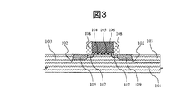
図3は、実施例3の半導体装置であるMISFETの断面図である。これは、五酸化ニオブ膜と五酸化タンタル膜との積層膜からなる誘電体膜をMISFETのゲート絶縁膜として用いた例である。
【0090】
まず、実施例1の半導体基板1と同様な半導体基板101を用意し、この半導体基板101の主面に素子分離領域の溝102およびその溝102内にシリコン酸化膜103を形成する。溝102およびシリコン酸化膜103の形成は実施例1の溝2およびシリコン酸化膜4と同様に行う。
【0091】
次に、半導体基板101の全面に五酸化ニオブを堆積し、これを結晶化して五酸化ニオブ膜104を形成する。さらに五酸化ニオブ膜104上に五酸化タンタルを堆積し、これを結晶化して五酸化タンタル膜105を形成する。五酸化ニオブの堆積およびその結晶化は、実施例1の五酸化ニオブ膜30を形成する工程と同様である。五酸化タンタルの堆積およびその結晶化は、実施例1の五酸化タンタル膜31を形成する工程と同様である。五酸化ニオブ膜104と五酸化タンタル膜105は後に説明するようにMISFETのゲート絶縁膜となるものである。
【0092】
次に、五酸化タンタル膜105上に、多結晶シリコンを堆積し、フォトレジスト膜をマスクとしてこの多結晶シリコン膜、五酸化タンタル膜105、五酸化ニオブ膜104をエッチングして除去する。これにより、多結晶シリコン膜からなるゲート電極106、および五酸化ニオブ膜104と五酸化タンタル膜105の積層膜からなるゲート絶縁膜を形成する。
【0093】
次に、フォトレジスト膜およびゲート電極106をマスクとして不純物を低濃度にイオン注入し、半導体領域107を形成する。また、全面にシリコン窒化膜またはシリコン酸化膜を形成し、これを異方性エッチングすることにより、ゲート電極106の側壁にサイドウォールスペーサ108を形成する。さらに、フォトレジスト膜、ゲート電極106およびサイドウォールスペーサ108をマスクとして不純物を高濃度にイオン注入し、半導体領域109を形成する。半導体領域107、109はいわゆるLDD構造のソース・ドレイン領域を構成する。
【0094】
このようにしてMISFETが形成される。この後、層間絶縁膜を形成し、半導体領域109に接する第1層配線を形成する。さらに上層の配線を、層間絶縁膜を介して形成する。これらの説明は実施例1の第1層配線等と同様であるため説明を省略する。
【0095】
上述した例では、ゲート電極106に多結晶シリコンを用いたが、これに限る必要はなく、窒化チタン、タングステン、窒化タングステンなどの金属電極を用いることができる。
【0096】
また、五酸化ニオブ膜104を形成する前に、半導体基板101の表面にシリコン窒化膜を形成してもよい。例えば、NH3熱処理して表面に窒化シリコン膜を形成する。このシリコン窒化膜は、誘電体膜の形成時および熱処理時に、チャネル領域である多結晶シリコンが酸化されるのを抑制する効果がある。
【0097】
本実施例3によれば、ゲート絶縁膜を五酸化ニオブ膜104と五酸化タンタル膜105の積層膜とするため、ゲート絶縁膜の結晶化熱処理温度を低温化でき、シリコン基板101の酸化を回避できる。
【0098】
また、五酸化ニオブ膜の高い誘電率によりゲート絶縁膜の容量を増大できるため、ゲート絶縁膜の膜厚を厚くし、リーク電流を低減することができる。すなわち、半導体装置の高集積化時にトランジスタの特性を維持するためには、従来のシリコン酸化膜で実現しようとすれば、膜厚を薄くして容量を維持しなければならず、トンネル電流が増加してしまうが、五酸化ニオブ膜104と五酸化タンタル膜105の積層膜によるゲート絶縁膜を用いると、容量が同じであれば膜厚を厚くすることができるので、トンネル電流を生じることの少ないMISFETを実現することができる。
【0099】
ゲート絶縁膜を基板とゲートで挟んだ部分は、いわゆるMIS構造のキャパシタとなっており、その部分に種々のキャパシタを適用し、それぞれのキャパシタによる効果を奏することができる。
【0100】
ここでは五酸化タンタル膜と五酸化ニオブ膜を2段階で形成したが、3段階以上で形成し膜厚を薄くすることで、各膜密度もより向上し、モフォロジが改善され、酸化熱処理時に膜中の残留炭素が抜けやすくなり、リーク電流が低減する。ただし、形成する段数が多くなるとプロセスコストが増大するため、3段階以下とするのが望ましい。
【0101】
また、キャパシタ誘電体膜の総膜厚一定の条件において、リーク電流低減の効果に着目し、誘電体膜の結晶化温度を下げるための下地である膜厚5nm以下の五酸化ニオブ膜の上にリーク電流を低減するため、膜厚5nmより厚い五酸化タンタル膜を形成してもよい。また、高誘電率化の効果に着目し、膜厚5nmより厚い五酸化ニオブ膜の上に、リーク電流低減のための膜厚5nm以下である五酸化タンタル膜を形成してもよい。
【0102】
なお、本発明によれば、上述の実施形態に限らず、本願明細書の課題を解決する手段の欄にあげた各種手段がそれぞれ適用可能であることはいうまでもない。
【0103】
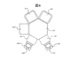
(実施例4)
図4は、実施例4における半導体製造装置の断面図である。
【0104】
本実施の形態の製造装置は、五酸化ニオブ膜を形成する第1反応室120と、五酸化タンタル膜を形成する第2反応室121と、五酸化ニオブ膜および五酸化タンタル膜に熱処理を行う第3反応室122とを有し、第1反応室120と第2反応室121と第3反応室122とは真空搬送室123にゲートバルブを介して接続されている。なおゲートバルブは図示を省略している。
【0105】
第1反応室120、第2反応室121および第3反応室122には各々基板加熱機構とガス供給機構とを備える。第1反応室120のガス供給機構は五酸化ニオブ膜をCVD法により形成するための原料ガスを供給する手段を有する。また、第2反応室121のガス供給機構は五酸化タンタル膜をCVD法により形成するための原料ガスを供給する手段を有する。また、第3反応室122のガス供給機構には酸素、一酸化二窒素あるいはオゾン等の酸化性ガスまたは不活性ガスを供給する手段を有する。
【0106】
真空搬送室123には、図示しないゲートバルブを介してロードロック室124、125が接続され、ロードロック室124、125には、各々カセット室126、127が接続される。カセット室126、127には各々ウェハカセットに保持されたウェハ128、129がセットされる。
【0107】
ウェハ128は、カセット室126からロードロック室124を介して真空搬送室123に導入される。この際、ロードロック室124では真空排気が行われ、真空搬送室123には大気は混入しない。このため真空搬送室123、第1反応室120、第2反応室121、および第3反応室122の清浄度が高く維持される。
【0108】
真空搬送室123に導入されたウェハ128は、第1反応室120に搬入されて実施例1〜3で説明したように五酸化ニオブが堆積される。この後、ウェハ128は第1反応室120から真空搬送室123を介して第3反応室122に搬入される。第3反応室122においては、ウェハ128に実施例1〜3で説明した熱処理が施され、五酸化ニオブ膜が結晶化される。
【0109】
次に、ウェハ128は第3反応室122から真空搬送室123を介して第2反応室121に搬入される。第2反応室121に搬入されたウェハ128は、実施例1〜3で説明したように五酸化タンタルが堆積される。この後、ウェハ128は第2反応室121から真空搬送室123を介して第3反応室122に搬入される。第3反応室122においては、ウェハ128に実施例1〜3で説明した熱処理が施され、五酸化タンタル膜が結晶化される。
【0110】
結晶化した五酸化タンタル膜が形成されたウェハ128は、真空搬送室123からロードロック室125を介してカセット室127に搬出され、ウェハ129としてウェハカセットに保持される。
【0111】
以上の工程により、多結晶化した五酸化ニオブと多結晶化した五酸化タンタルの積層膜が形成される。この間、ウェハ128は、高真空度に保持された真空搬送室123を介して移動するため、五酸化ニオブ膜等の界面は清浄に保たれ、良質な結晶膜の形成がなされる。すなわち、一般的には大気中の不純物、塵等の異物は五酸化ニオブ膜と五酸化タンタル膜の異常結晶化等を促進し、好ましくない欠陥を生ずる恐れがあるが、本実施の形態の製造装置を用いれば、高い洗浄度が実現できる高真空環境下での一貫した膜形成および結晶化の工程を実現できる。
【0112】
本実施例4によると、良質な多結晶構造を持つ五酸化ニオブ膜と五酸化タンタル膜の積層膜を形成することが可能となり、これを用いたDRAMの性能および信頼性を向上することができる。また、この積層膜をゲート絶縁膜に用いたMISFETの性能および信頼性を向上することができる。
【0113】
上述した例に加えて、真空搬送室123にさらに第4反応室を備え、この第4反応室において実施例2または3で説明したシリコン窒化膜を形成するための窒化処理を行うこともできる。この窒化処理は、第1反応室120での処理に先だって行われる。
【0114】
さらに、真空搬送室123に第5反応室を備え、この第5反応室において実施例1〜3で説明した上部電極を構成する窒化チタンその他の導電膜の堆積を行ってもよい。この導電膜の堆積は、第3反応室122の処理の後に行われる。
本実施例4によれば、積層膜を構成する五酸化ニオブ膜と五酸化タンタル膜の清浄度を保持することができ、誘電体膜の絶縁耐圧を向上して半導体装置の性能および信頼性を向上できる。加えて、製造のスループットを向上させることができる。
【0115】
また、五酸化ニオブ膜の形成と五酸化タンタル膜の形成を一つの反応室で行ってもよい。この場合、例えば第1の反応室120のガス供給機構は、五酸化ニオブ膜をCVD法により形成するための原料ガスを供給する手段と、五酸化タンタル膜をCVD法により形成するための原料ガスを供給する手段との両方を有し、第3反応室122において五酸化ニオブ膜が結晶化された後、真空搬送室123を介して再び第1反応室120に搬入され、五酸化タンタル膜が堆積される。この後、真空搬送室123を介して第3反応室122に搬入され、五酸化タンタル膜が結晶化される。
【0116】
この方法によれば、五酸化ニオブと五酸化タンタルを同一の反応室で堆積できるため、製造装置のコスト、ひいてはかかる半導体製造装置を用いて製造した半導体装置のコストを減少させることができる。
【0117】
上述した例では、五酸化タンタル膜と五酸化ニオブ膜との積層膜を持つキャパシタの製造を例に示したが、五酸化ニオブの積層膜又は五酸化タンタルと五酸化ニオブの混合物からなる積層膜を製造することもできる。
【0118】
本発明の第2手段による五酸化ニオブを積層する方法のように、誘電体膜を同じ原料ガスを用いて積層する場合には、反応室が2つ必要ないことはもとより、異なる2種の原料ガスを扱う必要が無いので、より低コストとなる。また、五酸化タンタルと五酸化ニオブの混合物からなる膜により積層膜を形成する方法も同様に低コストとなる。ペンタエトキシタンタルとペンタエトキシニオブのカクテル原料はペンタエトキシニオブのみの原料より、混ぜなければならない等、取り扱いに若干の手間がかかるが、異なる原料ガスにより積層膜を形成する場合よりは製造工程が複雑とならないからである。
【0119】
なお、本発明によれば、上述の実施形態に限らず、本願明細書の課題を解決する手段の欄にあげた各種手段がそれぞれ適用可能であることはいうまでもない。
【0120】
(実施例5)
発明の実施例5を図5で説明する。これは、五酸化ニオブの積層膜からなる誘電体膜を用いたMIMキャパシタである。例えば、このMIMキャパシタは、図1に示した半導体記憶装置、特にDRAM、のキャパシタに適用できるものである。図5中の下部電極206、五酸化ニオブ膜207、五酸化ニオブ膜208、上部電極209は図1中の下部電極29、五酸化ニオブ膜30、五酸化タンタル膜31、上部電極32の部分に対応するものである。
【0121】
まず、下部電極の形成までの工程について、図5(a)を用いて説明する。シリコン酸化膜からなるプラグ部層間絶縁膜201の内部にバリアメタルであるプラグ203を形成する。プラグ203は、下部電極206と多結晶シリコンからなるプラグ202との反応を抑制するために必要なものである。これにより、プラグ203とプラグ202との間に、導通を阻害する物質、例えばシリコン酸化物の形成を抑制して、情報蓄積用容量素子とメモリセル選択用MISFETとの接続を良好に維持することができる。プラグ203は、プラグ部層間絶縁膜201及びプラグ202の上部に、例えば窒化チタン膜をスパッタリング法あるいはCVD法により堆積し、これをエッチバックしてプラグ202の上部に残すことによって形成する。エッチバックに代えて、CMP法によって窒化チタン膜を研磨して除去してもよい。なお、プラグ203は、前記窒化チタン膜等の金属化合物に限らず、アルミを添加した窒化チタンや窒化タンタル、シリコンを添加した窒化タンタル、などにより構成してもよい。
【0122】
その後、シリコン窒化膜204とシリコン酸化膜からなるキャパシタ部層間絶縁膜205を形成し、プラグ203が露出するようにキャパシタ部層間絶縁膜205とシリコン窒化膜204に溝を形成する。キャパシタ部層間絶縁膜205は、例えばオゾン(O3)とテトラエトキシシラン(TEOS)とをソースガスに用いるプラズマCVD法によって形成する。また、溝はフォトレジスト膜をマスクとしたエッチングにより加工する。
【0123】
次に、ルテニウムからなる下部電極206を堆積する。まず、スパッタリング法によって、基板の全面に、膜厚が50nmのルテニウム膜を堆積する。スパッタリング法は段差被覆性に乏しいため、溝の内部には数nmのルテニウム膜しか形成されない。このスパッタリング法によるルテニウム膜を種層として、CVD法によって、基板の全面に、膜厚が20nmのルテニウム膜を形成する。このCVD法によるルテニウム膜は、有機金属錯体Ru(C2H4C2H5)2 (ビスエチルシクロペンタジエニルルテニウム)を(C2H4)2O (テトラヒドロフラン)に0.1mol/lの濃度で溶解した溶液を液体搬送して形成する。基板と対面するシャワーヘッド内で、液体原料を酸素ガスおよび窒素ガスと混合し、基板に吹きつける。形成温度は290℃、圧力は5Torrである。ここで、後の熱処理によってルテニウム膜が変形するのを防ぐために、焼き締めておくことが望ましい。具体的には、不活性雰囲気中、例えばアルゴン中で、700℃、1分間の熱処理を行えばよい。
【0124】
次に、基板の全面に絶縁膜(図示せず)を堆積する。絶縁膜は、溝への埋め込み性およびキャパシタ部層間絶縁膜205とのエッチング選択性を考慮してSOG膜とすることが好ましい。ここで、溝の内部を除くキャパシタ部層間絶縁膜205上のルテニウム膜を除去する。これらの除去にはエッチバック法あるいはCMP法を用いることができる。溝の内部に残存する絶縁膜(図示せず)はウェットエッチングにより除去することが可能である。このようにしてルテニウムからなる下部電極206が形成される(図5(a))。
【0125】
次に、基板の全面に膜厚が5nm以下の五酸化ニオブ膜207を堆積する(図5(b))。五酸化ニオブ膜207の堆積は、例えばペンタエトキシニオブ(Nb(C2H5O)5)を含むガスを原料ガスとし、500℃以下の減圧状態(例えば400mTorr)におけるCVD法により形成できる。また、例えばペンタエトキシニオブと酸化剤(例えばH2O)を交互に供給する原子層CVD法によって形成することもできる。
【0126】
五酸化ニオブは結晶化温度が低いため、膜の形成直後に五酸化ニオブ膜は部分的に結晶化するが、十分な誘電特性を得るためにはさらに結晶化のための熱処理が必要である。また、有機化合物原料から炭素が膜中に多く混入しており、リーク電流増加等の電気的特性に悪影響を及ぼすので、五酸化ニオブ膜207を酸化熱処理する必要がある。ここでは、結晶化熱処理と酸化熱処理を同時に行う。この熱処理は、下部電極及びバリアメタルが酸化しない温度の目安である700℃以下の温度で行われ、良好な多結晶構造を持つ五酸化ニオブ膜を得るために五酸化ニオブが十分に結晶化する目安である500℃以上の温度で行われることが望ましい。例えば、酸素や一酸化二窒素ガス雰囲気中、処理温度500℃〜700℃、処理時間1分〜10分の条件を例示できる。
【0127】
この熱処理によって、五酸化ニオブ膜207の結晶性の向上により誘電率が増加し、膜中の炭素量の減少によりリーク電流は減少する。
【0128】
次に、基板の全面に膜厚が5nm以下の五酸化ニオブ膜208を堆積する(図5(c))。五酸化ニオブ膜208の堆積は、前述した五酸化ニオブ膜207の堆積と同様の条件で形成すればよい。
【0129】
次に、五酸化ニオブ膜208に熱処理を行う。この熱処理は、前述した五酸化ニオブ膜207の熱処理と同様の条件で行えばよい。
【0130】
次に、五酸化二オブ膜208上に窒化チタン膜を例えばCVD法により堆積し、その窒化チタン膜上にフォトレジスト膜を形成し、このフォトレジスト膜をマスクとして窒化チタン膜、五酸化二オブ膜208及び五酸化ニオブ膜207をエッチングして容量絶縁膜および上部電極209を形成する(図5(d))。
【0131】
このようにして、ルテニウムからなる下部電極206、五酸化ニオブ膜207と五酸化二オブ膜208の積層膜からなるキャパシタ誘電体膜、および窒化チタンからなる上部電極209で構成される情報蓄積用容量素子を形成できる。例えば、この情報蓄積用容量素子をDRAMメモリセル選択用MISFETと直列に接続することとでDRAMのメモリセルが構成できる。
【0132】
なお、下部電極206を構成する材料としては、ルテニウム膜に代えて、白金膜、あるいは銅膜とすることができる。また、上部電極209を構成する材料としては、窒化チタン膜に代えて、タングステン膜、あるいはルテニウム膜とすることができる。ルテニウムからなる上部電極の場合は、下部電極206と同様の条件で形成すればよい。
【0133】
本実施例5によれば、キャパシタ誘電体膜として五酸化ニオブ膜を用いるため、キャパシタ誘電体膜の結晶化に要する熱処理温度を低温化でき、プラグ203の酸化による導通不良を回避できる。また、キャパシタ誘電体膜を積層膜により構成し、誘電体膜中の結晶粒界を分断することで、リーク電流を低減することができる。その積層膜を構成する五酸化ニオブ膜の膜厚を5nm以下にすることで、酸化熱処理の効率を良くし残留炭素を低減でき、膜のストレスが低減し、膜密度が向上し、モフォロジが改善される結果として、上部電極209と下部電極206との間のリーク電流をさらに低減し、DRAMのリフレッシュ特性を改善できる。
【0134】
ここでは、膜厚5nm以下である五酸化ニオブ膜と膜厚5nm以下である五酸化ニオブ膜を2段階で形成したが、これに限らず、例えばキャパシタ誘電体膜の総膜厚一定の条件において、各層全てが薄ければ最大の効果が得られるが、膜厚5nm以下の五酸化ニオブ膜の上に膜厚5nmより厚い五酸化ニオブ膜を形成する、もしくは膜厚5nmより厚い五酸化ニオブ膜の上に、膜厚5nm以下である五酸化ニオブ膜を形成しても、上記の結晶粒界の分断によるリーク電流低減の効果と膜厚が薄いことによるリーク電流低減の効果を得ることができる。
【0135】
また、誘電体膜は2段階形成に限る必要は無く、3段階以上で形成し、1層当たりの膜厚を薄くすることで、結晶粒界の分断によるリーク電流低減の効果と残留炭素減少によるリーク電流低減の効果を大きくすることができる。ただし、形成する段数が多くなるとプロセスコストが増大するため、3段階以下とするのが望ましい。
【0136】
実施例5において、キャパシタ誘電体膜に使用した五酸化二オブ膜に代えて、五酸化二オブと五酸化タンタルの混合物からなる膜を用いることもできる。その効果を得るための二オブとタンタルの組成比は、キャパシタに要求される仕様に応じて任意に選択すればよいが、誘電体膜の結晶化温度を下部電極及びバリアメタルが酸化しない低温の目安である700℃以下とするためには、下層の膜中の二オブに対するタンタルの組成比を90%以下とする必要がある。
【0137】
なお、本発明によれば、上述の実施形態に限らず、本願明細書の課題を解決する手段の欄にあげた各種手段がそれぞれ適用可能であることはいうまでもない。
【0138】
(実施例6)
発明の実施例6を図6で説明する。これは、五酸化ニオブの積層膜からなる誘電体膜を用いて、多結晶シリコンを下部電極に用いるMISキャパシタを形成する工程である。例えば、このMISキャパシタは、図2に示した半導体記憶装置、特にDRAM、のキャパシタに適用できるものである。図6中の下部電極210、五酸化ニオブ膜207、五酸化ニオブ膜208、上部電極209は図2の下部電極29、五酸化ニオブ膜30、五酸化タンタル膜31、上部電極32の部分に対応するものである。
【0139】
まず、シリコン酸化膜からなるプラグ部層間絶縁膜201の内部にプラグ202を形成する。プラグ202は、N型不純物(例えばP(リン))をドープした多結晶シリコン膜をCVD法で堆積した後、この多結晶シリコン膜をエッチバックしてスルーホールの内部に残すことにより形成する。エッチバックに代えて、CMP法により多結晶シリコン膜を研磨して除去してもよい。
【0140】
その後、実施例5と同様に、シリコン窒化膜204とキャパシタ部層間絶縁膜205を形成し、プラグ202が露出するようにシリコン窒化膜204とキャパシタ部層間絶縁膜205に溝を形成する。
【0141】
次に、膜厚20nmの導電性非晶質シリコン層を溝の内面およびキャパシタ部層間絶縁膜205の上面に渡って形成し、フォトリソグラフィ法およびドライエッチング法によりキャパシタ部層間絶縁膜205の上面の非晶質シリコン層を除去して、深孔の内面にのみ非晶質シリコン層を残す。溝内表面にシリコンの種付けをした後、630℃で熱処理して結晶化すると同時に表面を凹凸化して多結晶シリコンからなる下部電極210を形成する(図6(a))。
【0142】
次に、多結晶シリコンからなる下部電極210の表面にPH3を用いてPをドープした後、NH3熱処理して表面に窒化シリコン膜を形成する。膜厚は2nm程度と非常に薄いため、図6中には図示していない。このシリコン窒化膜は、誘電体膜の形成時および熱処理時に、下部電極の多結晶シリコンが酸化されるのを抑制する効果がある。
【0143】
次に、基板の全面に膜厚が5nmの五酸化ニオブ膜207を堆積する(図6(b))。五酸化ニオブ膜207の堆積は、実施例5と同様に行う。さらに、実施例5と同様に、五酸化ニオブ膜207に熱処理を行う。
【0144】
次に、五酸化ニオブ膜207上に五酸化ニオブ膜208を堆積する(図6(c))。五酸化ニオブ膜208の堆積は、実施例5と同様に行う。さらに、実施例5と同様に、五酸化ニオブ膜208に熱処理を行う。
【0145】
この後の工程は、実施例5とほぼ同様である(図6(d))。
【0146】
このようにして、多結晶シリコンからなる下部電極210、五酸化ニオブ膜207と五酸化二オブ膜208の積層膜からなる容量絶縁膜、および窒化チタンからなる上部電極209で構成される情報蓄積用容量素子を形成できる。これにより、メモリセル選択用MISFETとこれに直列に接続された情報蓄積用容量素子とで構成されるDRAMのメモリセルが完成する。
本実施例6によれば、キャパシタ誘電体膜として五酸化ニオブ膜を用いるため、キャパシタ誘電体膜の結晶化に要する熱処理温度を低温化でき、多結晶シリコンからなる下部電極210の酸化による容量低下を回避できる。また、キャパシタ誘電体膜を積層膜により構成し、誘電体膜中の結晶粒界を分断することで、リーク電流を低減することができる。その積層膜を構成する五酸化ニオブ膜の膜厚を5nm以下にすることで、酸化熱処理の効率を良くし残留炭素を低減でき、膜のストレスが低減し、膜密度が向上し、モフォロジが改善される結果として、上部電極209と下部電極210との間のリーク電流をさらに低減し、DRAMのリフレッシュ特性を改善できる。
【0147】
ここでは、膜厚5nm以下である五酸化ニオブ膜と膜厚5nm以下である五酸化ニオブ膜を2段階で形成したが、これに限らず、例えばキャパシタ誘電体膜の総膜厚一定の条件において、各層全てが薄ければ最大の効果が得られるが、膜厚5nm以下の五酸化ニオブ膜の上に膜厚5nmより厚い五酸化ニオブ膜を形成する、もしくは膜厚5nmより厚い五酸化ニオブ膜の上に、膜厚5nm以下である五酸化ニオブ膜を形成しても、上記の結晶粒界の分断によるリーク電流低減の効果と膜厚が薄いことによるリーク電流低減の効果を得ることができる。
【0148】
また、誘電体膜は2段階形成に限る必要は無く、3段階以上で形成し、1層当たりの膜厚を薄くすることで、結晶粒界の分断によるリーク電流低減の効果と残留炭素減少によるリーク電流低減の効果を大きくすることができる。ただし、形成する段数が多くなるとプロセスコストが増大するため、3段階以下とするのが望ましい。
【0149】
実施例6において、キャパシタ誘電体膜に使用した五酸化二オブ膜に代えて、五酸化二オブと五酸化タンタルの混合物からなる膜を用いることもできる。その効果を得るための二オブとタンタルの組成比は、キャパシタに要求される仕様に応じて任意に選択すればよいが、誘電体膜の結晶化温度を下部電極及びバリアメタルが酸化しない低温の目安である700℃以下とするためには、下層の膜中の二オブに対するタンタルの組成比を40%以下とする必要がある。このタンタルの組成比の上限が発明の実施例5で示したものよりも小さい理由は、シリコン上ではルテニウム上に比べて、タンタルの添加によって結晶化温度が増大する効果が大きいためである。
【0150】
実施例3において、ゲート絶縁膜を基板とゲートで挟んだ部分は、MIS構造のキャパシタとなっており、そのキャパシタの部分に発明の実施例6によるキャパシタを適用し、そのキャパシタによる効果を奏することができる。
【0151】
なお、本発明によれば、上述の実施形態に限らず、本願明細書の課題を解決する手段の欄にあげた各種手段がそれぞれ適用可能であることはいうまでもない。
【0152】
(実施例7)
発明の実施例7を図7で説明する。これは、五酸化ニオブ膜の積層からなる誘電体膜を用いて、多結晶シリコンを下部電極に用いるMISキャパシタを形成する工程である。例えば、このMISキャパシタは、図2に示した半導体記憶装置、特にDRAM、のキャパシタに適用できるものである。図7中の下部電極210、五酸化ニオブ膜207、五酸化ニオブ膜208、上部電極209は図2の下部電極29、五酸化ニオブ膜30、五酸化タンタル膜31、上部電極32の部分に対応するものである。ただし、下部電極の外側の側壁の一部をキャパシタとして利用する点が発明の実施例2と異なる。
【0153】
まず、シリコン酸化膜からなるプラグ部層間絶縁膜201の内部にプラグ202を形成する。プラグ202の形成は、実施例6と同様の方法で行えばよい。
【0154】
その後、シリコン窒化膜204、キャパシタ部層間絶縁膜205、シリコン窒化膜211、シリコン酸化膜212を順次形成し、フォトレジスト膜をマスクとしたエッチングによりプラグ202が露出するように溝を形成する。
【0155】
次に、膜厚20nmの導電性非晶質シリコン層を溝の内面およびシリコン酸化膜212の上面に渡って形成する(図7(a))。ここで、熱処理によって非晶質シリコン層を結晶化させ、多結晶シリコンを形成する。この結晶化熱処理は、非晶質シリコン層を円筒型に加工した後に行ってもよい。
【0156】
次に、基板の全面にシリコン酸化膜213を堆積する。シリコン酸化膜は、溝への埋め込み性を考慮してSOG膜とすることが好ましい。ここで、溝の内部を除くシリコン酸化膜212上の多結晶シリコン膜を除去する。これらの除去にはエッチバック法あるいはCMP法を用いることができる(図7(b))。
【0157】
ここで、溝の内部に残存するシリコン酸化膜213と、溝の外部のシリコン酸化膜212をウェットエッチングにより除去する。なお、シリコン窒化膜211がエッチングストッパーになるため、キャパシタ部層間絶縁膜205は除去されない。このようにして多結晶シリコンからなる円筒型の下部電極210が形成される(図7(c))。
【0158】
次に、NH3熱処理によって、多結晶シリコンからなる下部電極210の表面に窒化シリコン膜を形成する。膜厚は2nm程度と非常に薄いため、図7中には図示していない。このシリコン窒化膜は、誘電体膜の形成時および熱処理時に、下部電極の多結晶シリコンが酸化されるのを抑制する効果がある。
【0159】
次に、基板の全面に膜厚が5nm以下の五酸化ニオブ膜207を堆積する。五酸化ニオブ膜207の堆積は、実施例5と同様に行う。さらに、実施例5と同様に、五酸化ニオブ膜207に熱処理を行う。
【0160】
次に、五酸化ニオブ膜207上に、膜厚が5nm以下の五酸化ニオブ膜208を堆積する。五酸化ニオブ膜208の堆積は、実施例5と同様に行う。さらに、実施例5と同様に、五酸化ニオブ膜208に熱処理を行う。
【0161】
この後の工程は、実施例5とほぼ同様である(図7(d))。
【0162】
このようにして、多結晶シリコンからなる下部電極210、五酸化ニオブ膜207と五酸化二オブ膜208の積層膜からなる容量絶縁膜、および窒化チタンからなる上部電極209で構成される情報蓄積用容量素子を形成できる。これにより、メモリセル選択用MISFETとこれに直列に接続された情報蓄積用容量素子とで構成されるDRAMのメモリセルが完成する。
【0163】
なお、容量絶縁膜を構成する材料や形成段数の範囲については、実施例6で述べた内容と同様であるため、ここでは省略する。
【0164】
また、本実施の効果についても、実施例6で述べた内容とほぼ同様であるが、下部電極の外側にも誘電体膜を形成しているため、キャパシタ容量が大きい。
【0165】
本実施例7によれば、キャパシタ誘電体膜として五酸化ニオブ膜を用いるため、キャパシタ誘電体膜の結晶化に要する熱処理温度を低温化でき、多結晶シリコンからなる下部電極210の酸化による容量低下を回避できる。また、キャパシタ誘電体膜を積層膜により構成し、誘電体膜中の結晶粒界を分断することで、リーク電流を低減することができる。その積層膜を構成する五酸化ニオブ膜の膜厚を5nm以下にすることで、酸化熱処理の効率を良くし残留炭素を低減でき、膜のストレスが低減し、膜密度が向上し、モフォロジが改善される結果として、上部電極209と下部電極210との間のリーク電流をさらに低減し、DRAMのリフレッシュ特性を改善できる。
【0166】
ここでは、膜厚5nm以下である五酸化ニオブ膜と膜厚5nm以下である五酸化ニオブ膜を2段階で形成したが、これに限らず、例えばキャパシタ誘電体膜の総膜厚一定の条件において、各層全てが薄ければ最大の効果が得られるが、膜厚5nm以下の五酸化ニオブ膜の上に膜厚5nmより厚い五酸化ニオブ膜を形成する、もしくは膜厚5nmより厚い五酸化ニオブ膜の上に、膜厚5nm以下である五酸化ニオブ膜を形成しても、上記の結晶粒界の分断によるリーク電流低減の効果と膜厚が薄いことによるリーク電流低減の効果を得ることができる。
【0167】
また、誘電体膜は2段階形成に限る必要は無く、3段階以上で形成し、1層当たりの膜厚を薄くすることで、結晶粒界の分断によるリーク電流低減の効果と残留炭素減少によるリーク電流低減の効果を大きくすることができる。ただし、形成する段数が多くなるとプロセスコストが増大するため、3段階以下とするのが望ましい。
【0168】
実施例7において、キャパシタ誘電体膜に使用した五酸化二オブ膜に代えて、五酸化二オブと五酸化タンタルの混合物からなる膜を用いることもできる。その効果を得るための二オブとタンタルの組成比は、キャパシタに要求される仕様に応じて任意に選択すればよいが、誘電体膜の結晶化温度を下部電極及びバリアメタルが酸化しない低温の目安である700℃以下とするためには、下層の膜中の二オブに対するタンタルの組成比を40%以下とする必要がある。このタンタルの組成比の上限が発明の実施例5で示したものよりも小さい理由は、シリコン上ではルテニウム上に比べて、タンタルの添加によって結晶化温度が増大する効果が大きいためである。
【0169】
なお、本発明によれば、上述の実施例に限らず、本願明細書の課題を解決する手段の欄にあげた各種手段がそれぞれ適用可能であることはいうまでもない。
【0170】
(実施例8)
発明の実施例8を図8で説明する。これは、五酸化ニオブの積層からなる誘電体膜を用いて、例えばRFアナログデバイスとCMOSロジックデバイスをワンチップ内に集積する際に有効である平面型のMIMキャパシタを形成する工程である。
【0171】
まず、銅(Cu)からなる下部電極214を形成する。Cuは拡散係数が大きいため、誘電体膜を形成する前に、TaNなどのバリア層215を形成する必要がある(図8(a))。
【0172】
次に、基板の全面に膜厚が5nm以下の五酸化ニオブ膜207を堆積する(図8(b))。五酸化ニオブ膜207の堆積は、実施例5と同様に行う。さらに、実施例5と同様に、五酸化ニオブ膜207に熱処理を行う。
【0173】
次に、五酸化ニオブ膜207上に、膜厚が5nm以下の五酸化ニオブ膜208を堆積する(図8(c))。五酸化ニオブ膜208の堆積は、実施例5と同様に行う。さらに、実施例5と同様に、五酸化ニオブ膜208に熱処理を行う。
【0174】
次に、TaNなどのバリア層216を形成した後、Cuからなる上部電極217を形成する。
【0175】
このようにして、Cuからなる下部電極214、五酸化ニオブ膜207と五酸化二オブ膜208の積層膜からなる容量絶縁膜、およびCuからなる上部電極217で構成される情報蓄積用容量素子を形成できる。キャパシタの面積を規定するためにはそれぞれの層を加工する必要があるが、その工程は求められる形状に応じて任意に選択すればよい。
【0176】
本実施例8によれば、容量絶縁膜として五酸化ニオブ膜を用いるため、容量絶縁膜の結晶化に要する熱処理温度を低温化できる。また、多結晶化した五酸化二オブ膜を2段階で形成することにより、結晶性が高く、膜中の炭素量が少ない五酸化二オブ膜を形成できる。その結果、耐熱性の低いCu電極上においても誘電率の大きい容量絶縁膜が得られるため、情報蓄積用容量素子の蓄積電荷量を増大できる。また、上部電極217と下部電極214との間のリーク電流を低減できる。
【0177】
なお、本実施例8のような平面キャパシタでは、五酸化二オブ膜の形成方法として、CVD法ではなくスパッタリング法を用いることも十分考えられる。例えば、二オブ金属ターゲットを用いて、アルゴンと酸素の混合雰囲気中でスパッタリングすればよい。スパッタリング法では、有機金属化合物原料を用いないため、五酸化二オブ膜中に炭素は混入せず、結晶化温度を低温下する効果はあるが、膜中の残留炭素を低減する効果は有しない。しかし、多段階形成により、五酸化二オブ膜のリークパスとなる結晶粒界が分断されるため、キャパシタのリーク電流が低減できる。また、多段階形成し、一層当たりの膜厚を薄くすることで、五酸化二オブ膜のストレスが低減し、密度が向上し、モフォロジが改善され、リーク電流の低減に寄与する。
【0178】
本実施例8では、容量絶縁膜を構成する材料として五酸化ニオブを用いたが、五酸化二オブに代えて、五酸化二オブと五酸化タンタルの固溶体を用いてもよい。二オブとタンタルの組成比は、キャパシタに要求される仕様に応じて任意に選択すればよいが、誘電体膜の結晶化温度を下部電極及びバリアメタルが酸化しない低温の目安である700℃以下とするためには、二オブに対するタンタルの組成比を90%以下とする必要がある。
【0179】
また、誘電体膜は2段階形成に限る必要は無く、3段階以上で形成することで、結晶粒界の分断によるリーク電流低減の効果を大きくすることができ、1層当たりの膜厚を薄くすることで、膜質向上によるリーク電流低減の効果を大きくすることができる。ただし、形成する段数が多くなるとプロセスコストが増大するため、3段階以下とするのが望ましい。五酸化ニオブ膜の代わりに五酸化二オブと五酸化タンタルの混合物からなる膜を用いる場合でも同様である。
【0180】
本発明によれば、上述の実施形態に限らず、本願明細書の課題を解決する手段の欄にあげた各種手段がそれぞれ適用可能であることはいうまでもない。例えば、キャパシタ誘電体膜に実施例1の誘電体膜を用いて、その誘電体膜による効果を奏することができる。実施例8のMIM構造における下部電極をシリコンとし、MIS構造としても、熱処理温度が低く、リーク電流の少ないキャパシタを構成することができる。
【0181】
(実施例9)
発明の実施例9は、RFアナログデバイスとCMOSロジックデバイスをワンチップ内に集積した半導体集積回路の1例であり、そのロジック部、アナログ部、メモリ部の断面構造図である。この発明の実施例9においては、図9の312,313,314が発明の実施例8のMIMキャパシタに対応したものとなっている。ここでは、CMOS構造を前提として説明するが、バイポーラトランジスタとCMOSとを混在したいわゆるBiCMOS構造などにも本発明を適用できることはもちろんである。図9では、一つのP型シリコン基板P−SUB上にロジック部、アナログ部、メモリ部が形成されている。一つのP型シリコン基板P−SUB内部には、Nウェル領域302、303、304が島状に形成され、さらにそれぞれのNウェル領域の中に、Nウェル領域305、306、307およびPウェル領域308、309、310が図のように形成されている。またNウェル領域305、306、307にはPMOSトランジスタ、Pウェル領域308、309、310にはNMOSトランジスタが形成され、トランジスタの隣接部にはNウェル、Pウェル領域への給電部が示されている。さらに、アナログ部には多結晶シリコン配線層315で形成した抵抗成分が示されており、その他にはゲート酸化膜328、シリサイド層326、サイドスペーサ327、シリコン窒化膜325等が図に示されている。
【0182】
図9において、ロジック部のようにトランジスタをシリサイド化すると、拡散層領域におけるリーク電流が増加することがある。したがって、シリサイド化したトランジスタをメモリセルに利用すると、メモリセルのデータ保持特性を悪化させる場合がある。このような場合は、図9のようにPウェル領域310に形成したNMOSトランジスタをシリサイド化せずにメモリセルを形成してもよい。また特に図示していないが、多結晶シリコン配線層315は、シリサイド化をしないと抵抗値が大きくなるので、多結晶シリコン配線315上にタングステンW等を積層した、いわゆるポリメタル構造としてもよい。さらに多結晶シリコン配線層315上だけを選択的にシリサイド化して、拡散層領域をシリサイド化しないトランジスタ構造としてもよい。もちろん、リーク電流が保持特性に悪影響を及ぼさない程度であれば、ロジック部のトランジスタと同様にシリサイドしてもよい。その場合、シリサイド化させないための追加マスクが不要となり、より低コスト化できる。
【0183】
また、図9におけるウエル構造は、いわゆる3重ウェル構造であり、ロジック部、アナログ部、メモリ部をそれぞれNウェル領域302,303,304で分離している。これにより、ロジック部、アナログ部、メモリ部のそれぞれの領域は電気的に分離できるので互いの干渉を避けることができて安定に動作することが可能となる。また、それぞれの動作電圧に適したNウェル、Pウェルの電位を設定できる。もちろん、このように3重ウェル構造が必要ない場合には、Nウェル領域302,303,304のないより単純な構成にしてもよいし、メモリ部のみ、あるいはメモリ部とアナログ部のみをNウェル領域303,304で分離する、あるいは2つの領域を同じNウェル領域で囲むなど必要に応じて種々の変形が可能である。
【0184】
図9において、基板の上に示した破線は、金属配線層(320〜324)とそのコンタクト層(316〜319)の位置を示している。MIMキャパシタ312,313,314は、それぞれロジック部、アナログ部、メモリ部で利用されている。例えば、ロジック部では電源に接続される配線にキャパシタを設けることにより、電源の静電容量を増加させて電源を安定化することに利用できる。これをアナログ部やメモリ部にも使うことももちろん可能である。さらにアナログ部のキャパシタ素子や後述するようにメモリ部におけるメモリセルに応用することができる。
【0185】
従来の1T1Cセルにおいては、下部電極としては耐熱性等に優れた多結晶シリコンが主に用いられ、上部電極としてはTiNなどの耐酸化性を有する金属を用いてメモリキャパシタを形成していた。したがって、ロジックで用いられる金属配線層を、キャパシタの電極に用いることは困難であった。本実施例のMIMキャパシタは、下部電極として例えば第3層の金属配線層322を利用する。下部電極を形成した後、積層膜からなるキャパシタ誘電体膜を形成してさらに上部電極を形成する。このとき上部電極は第4層の金属配線層323と配線層322の間のビアホール318の層に形成される。このように、キャパシタの下部電極に配線層を利用すれば、ロジック部、アナログ部、メモリ部におけるキャパシタの片方の電極形成において、特別なプロセスが不要となる。またメモリ部においては、従来の立体構造を有する1T1Cセルとは異なり、キャパシタが平面構造であるためロジックの金属配線層を容易に利用でき、さらに平面構造であることから加工が容易であり、歩留まり良くキャパシタを形成できる。また配線層としては、例えばAlやCuを主成分とする金属配線などを利用できる。図面には記載していないが、各配線層にバリアメタルを利用することもできる。バリアメタルとしては、TiN、TaN等が挙げられる。
【0186】
本実施例9では、単純な平面構造のキャパシタであるといったことから、加工が容易であるためプロセスコストが低減できる。さらに、配線層をMIMキャパシタの電極に利用することで、メモリ部、ロジック部、アナログ部のキャパシタを同様の構造、および同様の材料で形成、コスト低減、信頼性や歩留まりの向上が実現できる。また、高誘電体膜として、五酸化ニオブ膜の積層膜を利用するので、結晶化温度を下げることができ、下部電極及びバリアメタルの酸化を防ぐことができ、キャパシタ容量低下及び導通不良を回避できる。
【0187】
ここでは、五酸化ニオブ膜の積層膜を有する平面キャパシタを用いたが、各実施例で示したような五酸化タンタルと五酸化ニオブの積層膜,又はx<yの関係を保つ(Ta1−xNbx)2O5/(Ta1−yNby)2O5),又は五酸化ニオブの積層膜,又は五酸化タンタルと五酸化ニオブの混合物からなる積層膜を用いた平面キャパシタを適用しても、それぞれのキャパシタによる効果を奏することができる。
【0188】
実施例9のキャパシタ312,313,314は平面構造であるが、実施例1,2,5,6,7の溝型構造のキャパシタを適用して、それぞれのキャパシタの効果を奏することができる。
【0189】
以上、本発明者によってなされた発明をその実施の形態に基づき具体的に説明したが、本発明は前記実施の形態に限定されるものではなく、その要旨を逸脱しない範囲で種々変更可能であることは言うまでもない。以下、例をあげておく。
【0190】
実施例1,5,8はそれぞれMIM構造を有するキャパシタであるため、各実施形態のキャパシタ誘電体膜はそれぞれ置き換えて用いることができ、それぞれの膜による効果を得ることができる。同様に、実施例2,6,7はそれぞれMIS構造であるため、各実施形態のキャパシタ誘電体膜はそれぞれ置き換えて用いることができ、それぞれの膜による効果を得ることができる。
【0191】
実施例3のゲート絶縁膜を基板とゲートで挟んだ部分は、MIS構造のキャパシタとなっており、そのキャパシタの部分に他の実施例2,6におけるキャパシタ誘電体膜を適用し、それぞれの誘電体膜による効果を奏することができる。
【0192】
実施例3において説明したMISFETは、はあらゆる半導体装置、例えばSRAM、電気的書き換え可能な一括消去型の読み出し専用メモリ、例えばDRAMのメモリセル選択用MISFETや、周辺回路のMISFETに適用できる。
【0193】
実施例1,2,5,6,7,8のキャパシタは、DRAMだけではなく、DRAMを混載したあらゆる半導体装置、あるいは、キャパシタを有するあらゆる半導体装置に適用できる。
【0194】
本実施例においては、実施例1,2,3,4における五酸化タンタル膜と五酸化ニオブ膜との積層膜による例と、実施例5,6,7,8において五酸化ニオブ膜どうしの積層膜による例を中心に説明したが、それぞれの実施形態において本明細書の課題を解決する手段の欄に記載した膜の組合せ、あるいは他の実施の形態で説明した膜の組合せを適宜適用できるものであり、それぞれに記載した効果を奏することができる。
【0195】
【発明の効果】
本発明の代表的な実施形態によれば、キャパシタ絶縁膜の熱処理温度を低温化することができるので、多結晶シリコン下部電極の酸化による容量の低下(MIS構造)や、バリアメタルの酸化によるコンタクト抵抗の増大(MIM構造)の抑制が可能となる。つまり、半導体容量素子の微細化による高集積化、工程簡略化および高信頼化による歩留まりの向上、等を実現することができる。さらに、五酸化タンタル単層に比べて誘電率を大きくすることが可能となる。これにより、信号量を増大させてデバイス動作の信頼性を向上させることが可能である。あるいは、キャパシタ高さを低減してプロセス負荷を低減することができる。
【0196】
キャパシタ誘電体膜を積層膜により構成し、誘電体膜中の結晶粒界を分断することで、リーク電流を低減することができる。また、その積層膜を構成する絶縁膜の膜厚を薄くすることで、膜のストレスが低減し、膜密度が向上し、モフォロジが改善される結果として、さらにリーク電流を低減することができる。
【図面の簡単な説明】
【図1】本発明の実施例1を説明する工程の縦断面図である。
【図2】本発明の実施例2を説明する工程の縦断面図である。
【図3】本発明の実施例3を説明する工程の縦断面図である。
【図4】本発明の実施例4を説明する工程の縦断面図である。
【図5】本発明の実施例5を説明する工程の縦断面図である。
【図6】本発明の実施例6を説明する工程の縦断面図である。
【図7】本発明の実施例7を説明する工程の縦断面図である。
【図8】本発明の実施例8を説明する工程の縦断面図である。
【図9】本発明の実施例8を用いた半導体集積回路のロジック部、アナログ部、メモリ部の断面構造図である。
【図10】MIM構造において、五酸化タンタル膜に添加するニオブの量が多いほど、結晶化温度が低温化し、同時に比誘電率が増大することを説明する図である。
【図11】MIS構造において、五酸化タンタル膜に添加するニオブの量が多いほど、結晶化温度が低温化し、同時に比誘電率が増大することを説明する図である。
【図12】五酸化タンタル膜に添加するニオブの量が多いほど、リーク電流密度が増大することを説明する図である。
【図13】五酸化タンタル膜と五酸化ニオブ膜の積層膜について、低温結晶化の効果を説明する図である。
【図14】五酸化タンタル膜と五酸化ニオブ膜との積層膜について、低リーク電流化の効果を説明する図である。
【図15】五酸化ニオブ膜の多段階形成によるリーク電流の低減の効果を説明する図である。
【符号の説明】
1・・・半導体基板、2・・・溝、3・・・シリコン酸化膜、4・・・シリコン酸化膜、5・・・N型半導体領域、6・・・P型ウエル、7・・・ゲート酸化膜、8・・・ゲート電極、9・・・シリコン窒化膜、10・・・N型半導体領域、11・・・シリコン窒化膜、12・・・SOG膜、13・・・シリコン酸化膜、14・・・シリコン酸化膜、15・・・コンタクトホール、16・・・コンタクトホール、17・・・プラグ、18・・・シリコン酸化膜、19・・・シリコン窒化膜、20・・・TiSi2層、21・・・サイドウォールスペーサ、22・・・SOG膜、23・・・シリコン酸化膜、24・・・シリコン酸化膜、25・・・スルーホール、26・・・プラグ、27・・・シリコン窒化膜、28・・・絶縁膜、29・・・下部電極、30・・・五酸化ニオブ膜、31・・・五酸化タンタル膜、32・・・上部電極、33・・・シリコン酸化膜、34・・・SOG膜、35・・・プラグ、36・・・第2層配線
101・・・半導体基板、102・・・溝、103・・・シリコン酸化膜、104・・・五酸化ニオブ膜、105・・・五酸化タンタル膜、106・・・ゲート電極、107・・・半導体領域、108・・・サイドウォールスペーサ、109・・・半導体領域、120・・・第1反応室、121・・・第2反応室、122・・・第3反応室、123・・・真空搬送室、124・・・ロードロック室、125・・・ロードロック室、126・・・カセット室、127・・・カセット室、128・・・ウェハ、129・・・ウェハ
201・・・プラグ部層間絶縁膜、202・・・プラグ、203・・・プラグ、204・・・シリコン窒化膜、205・・・キャパシタ部層間絶縁膜、206・・・下部電極、207・・・五酸化二オブ膜、208・・・五酸化二オブ膜、209・・・上部電極、210・・・下部電極、211・・・シリコン窒化膜、212・・・シリコン酸化膜、213・・・シリコン酸化膜、214・・・下部電極、215・・・バリア層、216・・・バリア層、217・・・上部電極
301・・・P型シリコン基板、302・・・Nウェル領域、303・・・Nウェル領域、304・・・Nウェル領域、305・・・Nウェル領域、306・・・Nウェル領域、307・・・Nウェル領域、308・・・Pウェル領域、309・・・Pウェル領域、310・・・Pウェル領域、311・・・素子分離酸化膜、312・・・MIMキャパシタ、313・・・MIMキャパシタ、314・・・MIMキャパシタ、315・・・多結晶シリコン配線層、316・・・ビアホール、317・・・ビアホール、318・・・ビアホール、319・・・ビアホール、320・・・第1層の金属配線層、321・・・第2層の金属配線層、322・・・第3層の金属配線層、323・・・第4層の金属配線層、324・・・第5層の金属配線層、325・・・シリコン窒化膜
326・・・シリサイド層、327・・・サイドスペーサ、328・・・ゲート酸化膜。[0001]
BACKGROUND OF THE INVENTION
The present invention relates to a semiconductor device and a manufacturing method thereof, and more particularly to a semiconductor device having a capacitor, for example, a DRAM (Dynamic Random Access Memory), and a technology effective when applied to the manufacturing method thereof.
[0002]
[Prior art]
Instead of silicon oxide film (relative dielectric constant: about 4) and silicon nitride film (relative dielectric constant: about 7), which have been used as capacitor dielectric film materials so far for high integration of semiconductor devices, etc., It is known to employ a tantalum pentoxide film having a relative dielectric constant as large as several tens (for example, JP-A-8-139288).
[0003]
As a method of manufacturing a capacitor having the tantalum pentoxide dielectric film, after forming a tantalum pentoxide film on the capacitor lower electrode, heat treatment is performed to crystallize the film, and a capacitor upper electrode is formed thereon. is there. The reason for heat-treating the tantalum pentoxide film is to obtain a capacitor having a large capacitance by utilizing the characteristics of tantalum pentoxide, which has a dielectric constant that increases when crystallized. However, in this manufacturing method, it is known that a heat treatment at a high temperature of 750 ° C. or higher is necessary in order to sufficiently crystallize the tantalum pentoxide film (for example, JP 2000-12796 A). . Hereinafter, the temperature of heat treatment performed to crystallize the dielectric film is referred to as crystallization heat treatment temperature.
[0004]
[Problems to be solved by the invention]
The capacitor structure will be described before describing the problems caused by the fact that a heat treatment at 750 ° C. or higher, which is a relatively high temperature, is required for crystallization.
[0005]
Capacitors that use a tantalum pentoxide film as a dielectric are large in MIS (Metal-Insulator-Semiconductor) structure using a polycrystalline silicon film as a lower electrode and MIM (Metal-Insulator-Metal) structure using a metal film as a lower electrode. Separated. As a difference between the MIS structure and the MIM structure, in addition to the difference in the lower electrode material, a barrier metal is required in the MIM structure. The barrier metal is formed between the lower electrode and the plug connected to the lower electrode, and is necessary for preventing the reaction between the lower electrode and the plug. If the plug and the lower electrode react, the electrical continuity is adversely affected. An example of the barrier metal is titanium nitride formed between a plug made of polycrystalline silicon and a lower electrode made of ruthenium.
[0006]
From here, the problem that a heat treatment at a relatively high temperature of 750 ° C. or higher is required for crystallization in the process of forming the tantalum pentoxide insulating film will be described. In the MIS structure, the silicon of the lower electrode is oxidized by this heat treatment, and the capacitor capacity is reduced. The reason is that silicon is more easily thermodynamically oxidized than tantalum, so that silicon reduces the tantalum pentoxide film during tantalum pentoxide crystallization heat treatment, resulting in the formation of a silicon oxide film with a low relative dielectric constant. Because it ends up. This problem of a reduction in the capacitance of the capacitor also occurs when a silicon nitride film is formed at the lower electrode interface in order to prevent silicon oxidation. This is because, for the same reason, the silicon nitride film is oxidized and the capacitance of the capacitor is reduced. Further, in the MIM structure, even if the metal electrode itself does not have an oxidation problem, the electric conductivity is impaired as a result of the barrier metal being oxidized by oxygen diffused in the electrode. The reason is that, for example, when the lower electrode is ruthenium, ruthenium has good oxygen permeability, and oxygen is dissolved in the lower electrode in the process of forming the tantalum pentoxide film. This is because the barrier metal is oxidized by the dissolved oxygen.
[0007]
Each problem in the MIS structure and MIM structure does not depend on the atmosphere during the crystallization heat treatment. When forming a capacitor using a tantalum pentoxide film, heat treatment may be performed in an oxygen atmosphere. Even if the oxidation of the lower electrode and the barrier metal can be suppressed by lowering the temperature of the oxidation heat treatment, the crystal If the temperature cannot be lowered, it will not be a fundamental solution to the problem.
[0008]
Since tantalum pentoxide is used as the capacitor dielectric film, it is extremely difficult to reduce the crystallization temperature to 750 ° C. or lower. The heat treatment performed in an oxygen atmosphere includes a heat treatment performed in an oxidizing atmosphere in order to repair oxygen vacancies in the capacitor dielectric film or a capacitor dielectric film formed by a CVD (Chemical Vapor Deposition) method or the like. There is a heat treatment or the like performed in an oxidizing atmosphere in order to remove residual carbon that causes leakage current.
[0009]
Therefore, in order to solve the problem based on the relatively high heat treatment temperature for crystallization of the tantalum pentoxide insulating film, niobium pentoxide was added to tantalum pentoxide, and changes in various properties were investigated.
[0010]
First, FIG. 10 shows experimental results in the MIM structure. As a sample, Pt (200 nm) / Ti (10 nm) / SiO 2 A film formed of a mixture of tantalum pentoxide and niobium pentoxide by a sputtering method on a (100 nm) / Si structure was used. The forming condition is 10 mTorr N 2 / O 2 Mixed gas (pressure ratio N 2 / O 2 = 1/1), the substrate temperature is 300 ° C., and the film thickness is 20 nm. After the insulating film was formed, heat treatment was performed in a nitrogen stream at 500 ° C. to 800 ° C. for 1 minute, and then in an oxygen stream at 500 ° C. for 2 minutes. FIG. 10 shows the crystallization temperature of the solid solution of tantalum pentoxide and niobium pentoxide formed under the above conditions and the relative dielectric constant after crystallization, with Nb ratios of 0%, 10%, 50%, 90%, and It is a comparison in each case of 100%. The horizontal axis indicates the amount of Nb added, and the vertical axis indicates the crystallization temperature and the relative dielectric constant. The Nb ratio is 0%, that is, the crystallization temperature of the tantalum pentoxide film is about 750 ° C., and the relative dielectric constant is about 30. When the amount of Nb added is increased, the crystallization temperature is lowered and the relative dielectric constant is increased at the same time. The Nb ratio is 100%, that is, the crystallization temperature of the niobium pentoxide film is about 500 ° C., and the relative dielectric constant is about 60. In order to suppress the oxidation of the lower electrode and the barrier metal to 700 ° C. or less that can be suppressed to a problem-free level, Nb may be added by 10% or more.
[0011]
Next, an experimental result in the MIS structure is shown in FIG. FIG. 11 shows the crystallization temperature of the solid solution of tantalum pentoxide and niobium pentoxide formed on silicon and the relative dielectric constant after crystallization, with Nb ratios of 0%, 10%, 50%, 90%, and 100. % In each case. The horizontal axis indicates the amount of Nb added, and the vertical axis indicates the crystallization temperature and the relative dielectric constant. The Nb ratio is 0%, that is, the crystallization temperature of the tantalum pentoxide film is about 750 ° C., and the relative dielectric constant is about 40. In order to suppress the oxidation of the lower electrode to a temperature of 700 ° C. or less that can suppress the oxidation to a problem, 60% or more of Nb may be added. When the amount of Nb added is increased, the crystallization temperature is lowered and the relative permittivity is increased at the same time as in FIG. 10, but the crystallization temperature is increased to about 750 ° C. with an Nb ratio of 50%. Is different from FIG.
[0012]
On the other hand, FIG. 12 compares the leakage current densities of the insulator films having different Nb ratios. The horizontal axis represents voltage, and the vertical axis represents leakage current density. The heat treatment temperature is 700 ° C. Increasing the amount of Nb increases the leakage current density.
[0013]
As described above, in order to avoid a relatively high heat treatment temperature when employing a tantalum pentoxide insulating film as a dielectric film, it is effective to apply a film added with niobium pentoxide or a pure niobium pentoxide film. However, as can be seen from FIG. 12, the inventors have found a problem that the leakage current density increases when niobium pentoxide is added.
[0014]
[Means for Solving the Problems]
Representative means for solving the above problems will be described below.
[0015]
According to the first means of the present invention, the insulator film of the capacitor is formed by a laminated film of a niobium pentoxide film and a tantalum pentoxide film.
[0016]
As is apparent from FIGS. 10, 11, and 12, the tantalum pentoxide film has a small leakage current but a high crystallization temperature. In contrast, a niobium pentoxide film has a low crystallization temperature but a large leakage current. Based on this result, it was considered that lamination of a tantalum pentoxide film and niobium pentoxide was effective. Specifically, first, a niobium pentoxide film is formed on the lower electrode, crystallized by a heat treatment at a temperature lower than 750 ° C., a tantalum pentoxide film is formed thereon, and the heat treatment is performed. Then, tantalum pentoxide is laminated on the base of the crystal structure of niobium pentoxide, and the crystallization temperature of the tantalum pentoxide film is lowered by the influence of the crystal structure of the niobium pentoxide film. At the same time, since the tantalum pentoxide film is present in the laminated film, the leakage current density can be kept small.
[0017]
In order to verify the effect of the laminated film, a tantalum pentoxide single layer film (Ta 2 O 5 ), Laminated film of tantalum pentoxide film and niobium pentoxide film (Ta 2 O 5 / Nb 2 O 5 ), And niobium pentoxide monolayer (Nb) 2 O 5 ) And the crystallization temperature and the leakage current density were compared. The tantalum pentoxide single layer film and the niobium pentoxide single layer film are formed by forming a single layer film having a thickness of 20 nm, followed by heat treatment in nitrogen at 500 ° C. to 750 ° C. for 1 minute, and further in oxygen at 500 ° C. for 2 minutes. It was formed by heat treatment. A laminated film of tantalum pentoxide and niobium pentoxide is formed by forming a niobium pentoxide film having a thickness of 5 nm on a silicon substrate and then performing a heat treatment at 500 ° C. for 1 minute in nitrogen, and forming a film on the niobium pentoxide film. After forming a tantalum pentoxide film having a thickness of 15 nm, a heat treatment was performed at 500 ° C. to 750 ° C. for 1 minute in nitrogen, and further a heat treatment was performed at 500 ° C. for 2 minutes in oxygen.
[0018]
FIG. 13 shows the heat treatment temperature dependence of the relative dielectric constant in each of the above dielectric films. The horizontal axis indicates the heat treatment temperature, and the vertical axis indicates the relative dielectric constant. The tantalum pentoxide single layer film is amorphous immediately after formation and has a relative dielectric constant of about 20. When heat treatment at 750 ° C. is performed, the tantalum pentoxide monolayer film crystallizes and the relative dielectric constant increases to about 30. On the other hand, the niobium pentoxide single layer film is amorphous immediately after formation and has a relative dielectric constant of about 30, but crystallizes by heat treatment at least at 500 ° C., and the relative dielectric constant increases to about 60. The laminated film of tantalum pentoxide and niobium pentoxide proposed in the present invention is already crystallized immediately after the formation of the tantalum pentoxide film, and has a relative dielectric constant of about 50. This is a result of lowering the crystallization temperature of the tantalum pentoxide film in order to form the tantalum pentoxide film on the crystal structure of the niobium pentoxide film that has already been crystallized. Normally, even when heat treatment is performed at a temperature at which tantalum pentoxide is difficult to crystallize, the tantalum pentoxide film on the niobium pentoxide film is sufficiently crystallized, and the relative dielectric constant increases to almost the same level as that of the niobium pentoxide single layer film. is doing.
[0019]
Next, comparison of leakage current densities is shown in FIG. The horizontal axis represents voltage, and the vertical axis represents leakage current density. The crystallization heat treatment temperature was 750 ° C. for the tantalum pentoxide single layer film, and 500 ° C. for the laminated film of the tantalum pentoxide film and the niobium pentoxide film and the niobium pentoxide single layer film. The leakage current of the niobium pentoxide film is much larger than that of the tantalum pentoxide film, but by stacking with the tantalum pentoxide film, almost the same characteristics as the tantalum pentoxide single layer film are obtained. This indicates that the leakage current in the laminated film of tantalum pentoxide and niobium pentoxide is governed by the tantalum pentoxide film.
[0020]
In other words, by laminating the tantalum pentoxide film and the niobium pentoxide film, the disadvantages of each are negated, so that the crystallization temperature of the tantalum pentoxide film is lowered to a crystallization temperature similar to that of a niobium pentoxide single layer film. In addition, a dielectric constant as high as that of a niobium pentoxide film was obtained, and at the same time, a capacitor having a low leakage current density equivalent to that of a tantalum pentoxide single layer film was realized.
[0021]
Although an example using a laminated film of a tantalum pentoxide film and a niobium pentoxide film is shown here, the present invention is not limited to this. The basic concept is to lower the crystallization temperature of the upper film by forming a dielectric film using a material that originally has a high crystallization temperature on a dielectric film that uses a material that has a low crystallization temperature. Thus, the upper electrode film having a leakage current characteristic superior to that of the lower film can be reduced by reducing the leakage current between the lower electrode and the upper electrode. For example, both the upper layer and the lower layer may be formed of a solid solution of tantalum pentoxide and niobium pentoxide. In this case, the upper layer film / lower layer film (Ta 1-x Nb x ) 2 O 5 / (Ta 1-y Nb y ) 2 O 5 ), It is effective to maintain the relationship of x <y. That is, it is sufficient that the niobium pentoxide content in the lower layer film is higher than the niobium pentoxide content in the upper layer film. The lower layer film that satisfies the above conditions can be crystallized at a temperature lower than that of the upper layer film, the crystallization temperature of the upper layer film can be lowered, and the leakage current can be reduced by the upper layer film having leakage current characteristics superior to those of the lower layer film. However, as the difference between the niobium pentoxide content of the formed upper film and the niobium pentoxide content of the lower film becomes smaller, this effect decreases.
[0022]
Next, according to the second means of the present invention, the insulator film of the capacitor is formed by a laminated film of niobium pentoxide films.
[0023]
Specifically, first, a niobium pentoxide film is formed on the lower electrode, crystallized by a low-temperature heat treatment, a niobium pentoxide film is formed thereon, and the heat treatment is performed. By using a niobium pentoxide film having a low crystallization temperature as the dielectric film, oxidation of the lower electrode and the barrier metal can be prevented. In addition, by forming the dielectric film in multiple stages, the crystal grain boundary that becomes a leak path is divided, and the film thickness per layer is reduced. Since it is easy to remove, the leakage current of the capacitor can be reduced. Further, what contributes to the reduction of leakage current includes reduction of film stress, improvement of film quality, and improvement of morphology by reducing the film thickness per layer.
[0024]
In order to verify the effect of the multistage formation of the niobium pentoxide film, a 10 nm thick niobium pentoxide film is formed on the polycrystalline silicon in one, two, and three stages, and the leakage current density Compared. The niobium pentoxide film was formed at a substrate temperature of 430 ° C. by a CVD method using pentaethoxyniobium and oxygen as source gases. The heat treatment conditions are 1 minute at 600 ° C. in an oxygen stream. FIG. 15 shows the effect of reducing the leakage current density by multi-stage formation. The horizontal axis represents voltage, and the vertical axis represents leakage current density. In the case of the one-step formation, the niobium pentoxide film was formed to a thickness of 10 nm and heat treatment was performed. In the case of two-stage formation, a 5 nm thick niobium pentoxide film was formed and heat-treated, and then a 5 nm thick niobium pentoxide film was formed and heat treated again. In the case of the three-stage formation, the niobium pentoxide film having a thickness of 3 nm is formed and heat-treated, and then the niobium pentoxide film having a thickness of 3 nm is formed and heat-treated again. went. As is apparent from FIG. 15, the leakage current is reduced by forming the niobium pentoxide film in multiple stages. One reason for this is that when the heat treatment temperature is lowered, oxygen is less likely to diffuse into the film, and the efficiency of removing carbon that should be discharged as carbon dioxide deteriorates. One solution is to reduce the film thickness per shot.
[0025]
In order to obtain the effect of reducing the leakage current to the maximum, it is desirable to make all the layers thin. However, the thickness of any one of the insulating films made of niobium pentoxide in the capacitor should be reduced. This effect can be obtained by reducing the thickness. This is because if the leakage current characteristic is improved even further, the leakage current characteristic is improved as a whole. Further, in the case of the laminated film of the tantalum pentoxide film and the niobium pentoxide film described as the first means, or the relationship of x <y is maintained (Ta 1-x Nb x ) 2 O 5 / (Ta 1-y Nb y ) 2 O 5 ), It is possible to increase the carbon removal efficiency by reducing the film thickness and to improve the leakage current characteristics of the entire laminated film.
[0026]
By using the above-described means, a capacitor having a high relative dielectric constant and a small leakage current can be realized even at a low temperature of 700 ° C. or lower.
[0027]
Although an example using a laminated film of a niobium pentoxide film and a niobium pentoxide film is shown here, the present invention is not limited to this. Even when a solid solution of tantalum pentoxide and niobium pentoxide is used as a material having a low crystallization temperature, a capacitor having the above characteristics can be realized.
[0028]
A method for laminating a niobium pentoxide film and a tantalum pentoxide film as a first means for solving the problem, and a niobium pentoxide film and a niobium pentoxide film as a second means for solving the problem Compare the effects of these methods.
[0029]
Both the first means and the second means can lower the crystallization temperature, prevent the lower electrode and the barrier metal from being oxidized, and reduce the leakage current. From the viewpoint of reducing the leakage current, the first means Is excellent. This is because a tantalum pentoxide film having a small leakage current is used as a dielectric film. In the case of forming by a CVD method from the viewpoint of manufacturing ease of semiconductor devices and cost reduction, the second means is excellent. Means for supplying a source gas for forming a niobium pentoxide film, and means for supplying a source gas for forming a tantalum pentoxide film in order to form each laminated dielectric film with the same material; This is because it is not necessary to have a separate gas, or it is not necessary to handle two different kinds of source gases for forming a laminated film.
[0030]
The matters common to the first and second means of the present invention can be summarized as follows. The dielectric film of the capacitor is made of a multi-layer insulator, so that the crystal grain boundaries are divided and the dielectric film under the capacitor is formed. Is a film containing niobium pentoxide, and the upper dielectric film is either a tantalum pentoxide film, a niobium pentoxide film, or a film made of a mixture of tantalum pentoxide and niobium pentoxide. The crystallization temperature of the body film can be lowered as compared with the case where a tantalum pentoxide film is used. As a result, oxidation of the lower electrode or barrier metal can be prevented, and a capacitor with good leakage current characteristics can be realized.
[0031]
This capacitor includes a capacitor having a dielectric film in which the lower film is a film made of a mixture of tantalum pentoxide and niobium pentoxide and the upper film is a niobium pentoxide film. In the case of this capacitor, the crystallization temperature of the material used for the lower layer film is higher than the crystallization temperature of the material used for the upper layer film, and is originally crystallized on the dielectric film using the material having a low crystallization temperature. By forming a dielectric film using a material having a high conversion temperature, there is no effect of lowering the heat treatment temperature of the upper film to the heat treatment temperature of the lower film. However, the heat treatment temperature for crystallizing the dielectric film is lower than the heat treatment temperature for crystallizing the conventional tantalum pentoxide film. As a result, oxidation of the lower electrode or the barrier metal due to heat treatment can be prevented.
[0032]
DETAILED DESCRIPTION OF THE INVENTION
Example 1
Hereinafter, embodiments of the present invention will be described in detail with reference to the drawings. Note that components having the same function are denoted by the same reference symbols throughout the drawings for describing the embodiments, and the repetitive description thereof will be omitted.
[0033]
A first embodiment of the invention will be described with reference to FIG. This is a case where the present invention is applied to a semiconductor memory device having a MIM capacitor using a dielectric film made of a laminated film of a niobium pentoxide film and a tantalum pentoxide film, particularly a DRAM.
[0034]
The manufacturing process of the DRAM will be described below.
[0035]
FIG. 1 is a cross-sectional view of a DRAM to which a capacitor of the present invention is applied. First, a P-type well 6 into which an element isolation region and impurities are introduced is formed in the
[0036]
Next, using the photoresist film (not shown) as a mask, the silicon nitride film and the silicon oxide film in the region where the
[0037]
Next, after removing the photoresist film, in order to remove the damaged layer formed on the inner wall of the
[0038]
Next, this silicon oxide film is polished by a CMP (Chemical Mechanical Polishing) method to remove the silicon oxide film in a region other than the
[0039]
Next, after the silicon oxide film and silicon nitride film remaining on the surface of the
[0040]
Next, after cleaning the surface of the
[0041]
Next, a
[0042]
Next, after removing the photoresist film, an etching solution such as hydrofluoric acid is used to remove dry etching residue, photoresist residue, and the like remaining on the surface of the
[0043]
Next, an N-type impurity, for example, P (phosphorus) is ion-implanted into the P-type well 6 to form an N-
[0044]
Next, after depositing a
[0045]
As described above, in this embodiment, the
[0046]
Next, the
[0047]
Next, after removing the photoresist film, an etching solution such as a hydrofluoric acid + ammonium fluoride mixed solution is used to remove dry etching residues and photoresist residues on the substrate surface exposed at the bottoms of the contact holes 15 and 16. To do. At that time, the
[0048]
Next, plugs 17 are formed inside the contact holes 15 and 16. The plug 17 is formed by depositing a polycrystalline silicon film doped with an N-type impurity (for example, P (phosphorus)) on the
[0049]
Next, after depositing a
[0050]
Next, the
[0051]
Next, sidewall spacers 21 are formed on the side walls of the bit lines BL. The sidewall spacer 21 is formed by depositing a silicon nitride film on the bit line BL by a CVD method and then anisotropically etching the silicon nitride film.
[0052]
Next, an
[0053]
Next, after depositing a
[0054]
Next, a silicon oxide film 24 having a thickness of about 100 nm is deposited on the
[0055]
Next, the
[0056]
Next, after removing the photoresist film, an etching solution such as a hydrofluoric acid + ammonium fluoride mixed solution is used to remove dry etching residue, photoresist residue, and the like on the surface of the plug 17 exposed at the bottom of the through
[0057]
Next, a
[0058]
Thereafter, a silicon nitride film 27 and an insulating
[0059]
Next, a
[0060]
Next, an insulating film (not shown) is deposited on the entire surface of the
[0061]
Next, a
[0062]
Next, the
[0063]
Next, a
[0064]
Next, the
[0065]
Thus, since the tantalum pentoxide film is formed on the polycrystallized niobium pentoxide film and heat-treated, the crystallization temperature of the tantalum pentoxide film can be lowered, and at the same time a high dielectric constant can be realized. Further, since the conduction mechanism of the leakage current is governed by the tantalum pentoxide film, the leakage current characteristic of the laminated film of the tantalum pentoxide film and the niobium pentoxide film is almost the same as that of the tantalum pentoxide single layer film.
[0066]
Next, a titanium nitride film is deposited on the
[0067]
In this manner, an information storage capacitive element including the
[0068]
Next, after removing the photoresist film, a silicon oxide film 33 having a thickness of about 40 nm is deposited on the information storage capacitor. The silicon oxide film 33 is made of, for example, ozone (O 3 ) And tetraethoxysilane (TEOS) are deposited by plasma CVD using a source gas. Further, the SOG film 34 is applied to flatten the region where the memory cell is formed, and at the same time, the step with the peripheral circuit region is relaxed.
[0069]
Next, through holes are formed by removing the SOG film 34 and the silicon oxide film 33 by dry etching using a photoresist film as a mask. Thereafter, a
[0070]
Thereafter, a third layer wiring is formed through an interlayer insulating film, and a passivation film composed of a silicon oxide film and a silicon nitride film is deposited on the third layer wiring, but illustration thereof is omitted. The third layer wiring and the plug connected to the third layer wiring can be formed in the same manner as the second layer wiring. The interlayer insulating film includes, for example, a silicon oxide film having a thickness of about 300 nm, an SOG film having a thickness of about 400 nm, and A silicon oxide film having a thickness of about 300 nm can be used. The silicon oxide film is made of, for example, ozone (O 3 ) And tetraethoxysilane (TEOS) can be deposited by plasma CVD using a source gas.
[0071]
Through the above steps, the DRAM of this embodiment is substantially completed.
[0072]
According to the first embodiment, since the capacitive insulating film is a laminated film of the
[0073]
In the example described above, the capacitive insulating film is a laminated film of the
[0074]
Here, the tantalum pentoxide film having a film thickness of 5 nm or less and the niobium pentoxide film having a film thickness of 5 nm or less were formed in two stages. However, the present invention is not limited to this, for example, under the condition that the total film thickness of the capacitor dielectric film is constant. Focusing on the effect of reducing the leakage current, in order to reduce the leakage current on the niobium pentoxide film having a film thickness of 5 nm or less, which is a base for lowering the crystallization temperature of the dielectric film, pentoxide thicker than 5 nm is used. A tantalum film may be formed. Further, paying attention to the effect of increasing the dielectric constant, a tantalum pentoxide film having a thickness of 5 nm or less for reducing leakage current may be formed on the niobium pentoxide film thicker than 5 nm.
The dielectric film need not be limited to the two-stage formation. By forming the film in three or more stages and reducing the film thickness, the density of each film is improved, the morphology is improved, and residual carbon in the film is eliminated during the oxidation heat treatment. The leakage current is reduced. However, if the number of stages to be formed increases, the process cost increases.
In addition, according to this invention, it cannot be overemphasized that the various means mention | raise | lifted to the column of the means to solve the subject of this-application specification are each applicable not only in the above-mentioned embodiment.
[0075]
(Example 2)
A second embodiment of the invention will be described with reference to FIG. This is an example in which a MIS capacitor using a dielectric film made of a laminated film of a niobium pentoxide film and a tantalum pentoxide film is applied to a semiconductor memory device, particularly a DRAM.
[0076]
The DRAM of the present embodiment is the same as that of the first embodiment except that the structure of the information storage capacitor is different. Therefore, in the following description, only the different parts will be described, and the description of similar parts will be omitted.
[0077]
The manufacturing method of the DRAM of the second embodiment is the same up to the step before the formation of the
[0078]
Thereafter, as in the first embodiment, a silicon nitride film 27 and an insulating
[0079]
Next, a conductive amorphous silicon layer having a thickness of 20 nm is formed over the inner surface of the groove and the upper surface of the insulating
[0080]
Next, PH is formed on the surface of the
[0081]
Next, a
[0082]
Next, a
[0083]
Subsequent steps are almost the same as those in the first embodiment.
[0084]
According to the second embodiment, since the capacitor insulating film is a laminated film of the
[0085]
In the example described above, the capacitive insulating film is a laminated film of the
[0086]
Here, the tantalum pentoxide film having a film thickness of 5 nm or less and the niobium pentoxide film having a film thickness of 5 nm or less were formed in two stages. However, the present invention is not limited to this, for example, under the condition that the total film thickness of the capacitor dielectric film is constant. Focusing on the effect of reducing the leakage current, tantalum pentoxide thicker than 5 nm is used to reduce the leakage current on the niobium pentoxide film having a thickness of 5 nm or less, which is a base for lowering the crystallization temperature of the dielectric film. A film may be formed. Further, paying attention to the effect of increasing the dielectric constant, a tantalum pentoxide film having a thickness of 5 nm or less for reducing leakage current may be formed on the niobium pentoxide film thicker than 5 nm.
[0087]
The dielectric film need not be limited to the two-stage formation. By forming the film in three or more stages and reducing the film thickness, the density of each film is improved, the morphology is improved, and residual carbon in the film is eliminated during the oxidation heat treatment. The leakage current is reduced. However, if the number of stages to be formed increases, the process cost increases.
[0088]
In addition, according to this invention, it cannot be overemphasized that the various means mention | raise | lifted to the column of the means to solve the subject of this-application specification are each applicable not only in the above-mentioned embodiment.
[0089]
(Example 3)
FIG. 3 is a cross-sectional view of a MISFET which is a semiconductor device according to the third embodiment. This is an example in which a dielectric film composed of a laminated film of a niobium pentoxide film and a tantalum pentoxide film is used as a gate insulating film of a MISFET.
[0090]
First, a
[0091]
Next, niobium pentoxide is deposited on the entire surface of the
[0092]
Next, polycrystalline silicon is deposited on the
[0093]
Next, impurities are ion-implanted at a low concentration using the photoresist film and the
[0094]
In this way, a MISFET is formed. Thereafter, an interlayer insulating film is formed, and a first layer wiring in contact with the
[0095]
In the above-described example, polycrystalline silicon is used for the
[0096]
Further, a silicon nitride film may be formed on the surface of the
[0097]
According to the third embodiment, since the gate insulating film is a laminated film of the
[0098]
Further, since the capacity of the gate insulating film can be increased by the high dielectric constant of the niobium pentoxide film, the thickness of the gate insulating film can be increased and the leakage current can be reduced. In other words, in order to maintain the transistor characteristics when the semiconductor device is highly integrated, if the conventional silicon oxide film is to be realized, the film thickness must be reduced to maintain the capacity, and the tunnel current increases. However, when a gate insulating film including a stacked film of the
[0099]
A portion where the gate insulating film is sandwiched between the substrate and the gate is a so-called MIS structure capacitor, and various capacitors can be applied to the portion, and the effect of each capacitor can be exhibited.
[0100]
Here, the tantalum pentoxide film and the niobium pentoxide film are formed in two stages, but by forming the film in three or more stages and reducing the film thickness, the density of each film is further improved, the morphology is improved, and the film is formed during the oxidation heat treatment. Residual carbon is easily removed, and leakage current is reduced. However, if the number of stages to be formed increases, the process cost increases.
[0101]
Also, paying attention to the effect of reducing the leakage current under the condition that the total thickness of the capacitor dielectric film is constant, on the niobium pentoxide film having a thickness of 5 nm or less as a base for lowering the crystallization temperature of the dielectric film. In order to reduce leakage current, a tantalum pentoxide film thicker than 5 nm may be formed. Further, paying attention to the effect of increasing the dielectric constant, a tantalum pentoxide film having a thickness of 5 nm or less for reducing leakage current may be formed on the niobium pentoxide film thicker than 5 nm.
[0102]
In addition, according to this invention, it cannot be overemphasized that the various means mention | raise | lifted to the column of the means to solve the subject of this-application specification are each applicable not only in the above-mentioned embodiment.
[0103]
(Example 4)
FIG. 4 is a cross-sectional view of the semiconductor manufacturing apparatus according to the fourth embodiment.
[0104]
The manufacturing apparatus of this embodiment performs heat treatment on the
[0105]
The
[0106]
[0107]
The
[0108]
The
[0109]
Next, the
[0110]
The
[0111]
Through the above steps, a laminated film of polycrystallized niobium pentoxide and polycrystallized tantalum pentoxide is formed. During this time, the
[0112]
According to the fourth embodiment, it is possible to form a laminated film of a niobium pentoxide film and a tantalum pentoxide film having a high-quality polycrystalline structure, and the performance and reliability of a DRAM using the same can be improved. . In addition, the performance and reliability of the MISFET using this laminated film as a gate insulating film can be improved.
[0113]
In addition to the above-described example, the
[0114]
Further, the
According to the fourth embodiment, the cleanliness of the niobium pentoxide film and the tantalum pentoxide film constituting the laminated film can be maintained, the dielectric breakdown voltage of the dielectric film is improved, and the performance and reliability of the semiconductor device are improved. It can be improved. In addition, the manufacturing throughput can be improved.
[0115]
Alternatively, the niobium pentoxide film and the tantalum pentoxide film may be formed in one reaction chamber. In this case, for example, the gas supply mechanism of the
[0116]
According to this method, since niobium pentoxide and tantalum pentoxide can be deposited in the same reaction chamber, the cost of the manufacturing apparatus, and thus the cost of the semiconductor device manufactured using such a semiconductor manufacturing apparatus can be reduced.
[0117]
In the above example, the production of a capacitor having a laminated film of a tantalum pentoxide film and a niobium pentoxide film is shown as an example. However, a laminated film of niobium pentoxide or a mixture of tantalum pentoxide and niobium pentoxide is used. Can also be manufactured.
[0118]
When the dielectric films are laminated using the same raw material gas as in the method of laminating niobium pentoxide according to the second means of the present invention, two different raw materials are used as well as two reaction chambers are not necessary. Since there is no need to handle gas, the cost is lower. Similarly, a method of forming a laminated film with a film made of a mixture of tantalum pentoxide and niobium pentoxide is also low in cost. The cocktail raw material of pentaethoxytantalum and pentaethoxyniobium needs to be mixed rather than the raw material of pentaethoxyniobium alone, but it takes some time to handle, but the manufacturing process is more complicated than the case of forming a laminated film with different raw material gases. It is because it does not become.
[0119]
In addition, according to this invention, it cannot be overemphasized that the various means mention | raise | lifted to the column of the means to solve the subject of this-application specification are each applicable not only in the above-mentioned embodiment.
[0120]
(Example 5)
[0121]
First, steps up to the formation of the lower electrode will be described with reference to FIG. A
[0122]
Thereafter, a capacitor part
[0123]
Next, a
[0124]
Next, an insulating film (not shown) is deposited on the entire surface of the substrate. The insulating film is preferably an SOG film in consideration of the embedding property in the trench and the etching selectivity with the capacitor portion
[0125]
Next, a
[0126]
Since niobium pentoxide has a low crystallization temperature, the niobium pentoxide film is partially crystallized immediately after the film is formed. However, in order to obtain sufficient dielectric properties, a heat treatment for crystallization is required. Further, since a large amount of carbon is mixed into the film from the organic compound raw material and adversely affects electrical characteristics such as an increase in leakage current, the
[0127]
By this heat treatment, the dielectric constant is increased by improving the crystallinity of the
[0128]
Next, a
[0129]
Next, the
[0130]
Next, a titanium nitride film is deposited on the
[0131]
In this way, the information storage capacitor comprising the
[0132]
Note that the material forming the
[0133]
According to the fifth embodiment, since the niobium pentoxide film is used as the capacitor dielectric film, the heat treatment temperature required for crystallization of the capacitor dielectric film can be lowered, and conduction failure due to oxidation of the
[0134]
Here, the niobium pentoxide film having a film thickness of 5 nm or less and the niobium pentoxide film having a film thickness of 5 nm or less are formed in two stages. However, the present invention is not limited to this, for example, under the condition that the total film thickness of the capacitor dielectric film is constant. The maximum effect can be obtained if all the layers are thin, but a niobium pentoxide film having a thickness of 5 nm or more is formed on a niobium pentoxide film having a thickness of 5 nm or less, or a niobium pentoxide film having a thickness of 5 nm or more. Even if a niobium pentoxide film having a film thickness of 5 nm or less is formed on the surface, it is possible to obtain the effect of reducing the leakage current by dividing the crystal grain boundary and the effect of reducing the leakage current due to the thin film thickness. .
[0135]
In addition, the dielectric film need not be limited to the two-stage formation, and is formed in three or more stages, and by reducing the film thickness per layer, the leakage current can be reduced by cutting the grain boundaries and the residual carbon can be reduced. The effect of reducing the leakage current can be increased. However, if the number of stages to be formed increases, the process cost increases.
[0136]
In Example 5, instead of the niobium pentoxide film used for the capacitor dielectric film, a film made of a mixture of niobium pentoxide and tantalum pentoxide can be used. The composition ratio of niobium and tantalum for obtaining the effect may be arbitrarily selected according to the specifications required for the capacitor. However, the crystallization temperature of the dielectric film is low enough not to oxidize the lower electrode and the barrier metal. In order to set the target temperature to 700 ° C. or lower, the composition ratio of tantalum to niobium in the lower layer film needs to be 90% or lower.
[0137]
In addition, according to this invention, it cannot be overemphasized that the various means mention | raise | lifted to the column of the means to solve the subject of this-application specification are each applicable not only in the above-mentioned embodiment.
[0138]
(Example 6)
[0139]
First, a
[0140]
Thereafter, as in the fifth embodiment, a
[0141]
Next, a conductive amorphous silicon layer having a thickness of 20 nm is formed over the inner surface of the trench and the upper surface of the capacitor portion
[0142]
Next, PH is formed on the surface of the
[0143]
Next, a 5 nm thick
[0144]
Next, a
[0145]
Subsequent steps are almost the same as those in Example 5 (FIG. 6D).
[0146]
In this way, for information storage composed of the
According to the sixth embodiment, since the niobium pentoxide film is used as the capacitor dielectric film, the heat treatment temperature required for crystallization of the capacitor dielectric film can be lowered, and the capacitance is reduced due to the oxidation of the
[0147]
Here, the niobium pentoxide film having a film thickness of 5 nm or less and the niobium pentoxide film having a film thickness of 5 nm or less are formed in two stages. However, the present invention is not limited to this, for example, under the condition that the total film thickness of the capacitor dielectric film is constant. The maximum effect can be obtained if all the layers are thin, but a niobium pentoxide film having a thickness of 5 nm or more is formed on a niobium pentoxide film having a thickness of 5 nm or less, or a niobium pentoxide film having a thickness of 5 nm or more. Even if a niobium pentoxide film having a film thickness of 5 nm or less is formed on the surface, it is possible to obtain the effect of reducing the leakage current by dividing the crystal grain boundary and the effect of reducing the leakage current due to the thin film thickness. .
[0148]
In addition, the dielectric film need not be limited to the two-stage formation, and is formed in three or more stages, and by reducing the film thickness per layer, the leakage current can be reduced by cutting the grain boundaries and the residual carbon can be reduced. The effect of reducing the leakage current can be increased. However, if the number of stages to be formed increases, the process cost increases.
[0149]
In Example 6, instead of the niobium pentoxide film used for the capacitor dielectric film, a film made of a mixture of niobium pentoxide and tantalum pentoxide can be used. The composition ratio of niobium and tantalum for obtaining the effect may be arbitrarily selected according to the specifications required for the capacitor. However, the crystallization temperature of the dielectric film is low enough not to oxidize the lower electrode and the barrier metal. In order to set the target temperature to 700 ° C. or lower, the composition ratio of tantalum to niobium in the lower layer film needs to be 40% or lower. The reason why the upper limit of the composition ratio of tantalum is smaller than that shown in Example 5 of the invention is that the effect of increasing the crystallization temperature by adding tantalum on silicon is larger than that on ruthenium.
[0150]
In the third embodiment, the portion where the gate insulating film is sandwiched between the substrate and the gate is a MIS structure capacitor, and the capacitor according to the sixth embodiment of the invention is applied to the capacitor portion, and the effect of the capacitor is exhibited. Can do.
[0151]
In addition, according to this invention, it cannot be overemphasized that the various means mention | raise | lifted to the column of the means to solve the subject of this-application specification are each applicable not only in the above-mentioned embodiment.
[0152]
(Example 7)
A seventh embodiment of the invention will be described with reference to FIG. This is a step of forming a MIS capacitor using polycrystalline silicon as a lower electrode, using a dielectric film made of a stack of niobium pentoxide films. For example, the MIS capacitor can be applied to the capacitor of the semiconductor memory device shown in FIG. 2, particularly the DRAM. The
[0153]
First, a
[0154]
Thereafter, a
[0155]
Next, a conductive amorphous silicon layer having a thickness of 20 nm is formed over the inner surface of the groove and the upper surface of the silicon oxide film 212 (FIG. 7A). Here, the amorphous silicon layer is crystallized by heat treatment to form polycrystalline silicon. This crystallization heat treatment may be performed after the amorphous silicon layer is processed into a cylindrical shape.
[0156]
Next, a
[0157]
Here, the
[0158]
Next, NH 3 A silicon nitride film is formed on the surface of the
[0159]
Next, a
[0160]
Next, a
[0161]
Subsequent steps are substantially the same as those in Example 5 (FIG. 7D).
[0162]
In this way, for information storage composed of the
[0163]
Note that the material constituting the capacitor insulating film and the range of the number of formation steps are the same as those described in
[0164]
The effect of the present embodiment is almost the same as that described in the sixth embodiment. However, since the dielectric film is formed outside the lower electrode, the capacitor capacity is large.
[0165]
According to the seventh embodiment, since the niobium pentoxide film is used as the capacitor dielectric film, the heat treatment temperature required for crystallization of the capacitor dielectric film can be lowered, and the capacitance is reduced due to oxidation of the
[0166]
Here, the niobium pentoxide film having a film thickness of 5 nm or less and the niobium pentoxide film having a film thickness of 5 nm or less are formed in two stages. However, the present invention is not limited to this, for example, under the condition that the total film thickness of the capacitor dielectric film is constant. The maximum effect can be obtained if all the layers are thin, but a niobium pentoxide film having a thickness of 5 nm or more is formed on a niobium pentoxide film having a thickness of 5 nm or less, or a niobium pentoxide film having a thickness of 5 nm or more. Even if a niobium pentoxide film having a film thickness of 5 nm or less is formed on the surface, it is possible to obtain the effect of reducing the leakage current by dividing the crystal grain boundary and the effect of reducing the leakage current due to the thin film thickness. .
[0167]
In addition, the dielectric film need not be limited to the two-stage formation, and is formed in three or more stages, and by reducing the film thickness per layer, the leakage current can be reduced by cutting the grain boundaries and the residual carbon can be reduced. The effect of reducing the leakage current can be increased. However, if the number of stages to be formed increases, the process cost increases.
[0168]
In Example 7, instead of the niobium pentoxide film used for the capacitor dielectric film, a film made of a mixture of niobium pentoxide and tantalum pentoxide may be used. The composition ratio of niobium and tantalum for obtaining the effect may be arbitrarily selected according to the specifications required for the capacitor. However, the crystallization temperature of the dielectric film is low enough not to oxidize the lower electrode and the barrier metal. In order to set the target temperature to 700 ° C. or lower, the composition ratio of tantalum to niobium in the lower layer film needs to be 40% or lower. The reason why the upper limit of the composition ratio of tantalum is smaller than that shown in Example 5 of the invention is that the effect of increasing the crystallization temperature by adding tantalum on silicon is larger than that on ruthenium.
[0169]
In addition, according to this invention, it cannot be overemphasized that the various means mention | raise | lifted to the column of the means to solve the subject of this-application specification are each applicable not only in the above-mentioned Example.
[0170]
(Example 8)
An eighth embodiment of the invention will be described with reference to FIG. This is a process of forming a planar MIM capacitor that is effective when, for example, an RF analog device and a CMOS logic device are integrated in one chip, using a dielectric film made of a stack of niobium pentoxide.
[0171]
First, the
[0172]
Next, a
[0173]
Next, a
[0174]
Next, after forming a
[0175]
In this manner, an information storage capacitive element composed of the
[0176]
According to the eighth embodiment, since the niobium pentoxide film is used as the capacitor insulating film, the heat treatment temperature required for crystallization of the capacitor insulating film can be lowered. Further, by forming a polycrystallized niobium pentoxide film in two stages, a niobium pentoxide film having high crystallinity and a small amount of carbon in the film can be formed. As a result, a capacitive insulating film having a large dielectric constant can be obtained even on a Cu electrode having low heat resistance, so that the amount of stored charge in the information storage capacitive element can be increased. Further, the leakage current between the
[0177]
In the planar capacitor as in Example 8, it is sufficiently conceivable to use the sputtering method instead of the CVD method as the method for forming the niobium pentoxide film. For example, sputtering may be performed using a niobium metal target in a mixed atmosphere of argon and oxygen. In the sputtering method, since no organic metal compound raw material is used, carbon is not mixed in the niobium pentoxide film, and there is an effect of lowering the crystallization temperature, but there is no effect of reducing residual carbon in the film. . However, since the crystal grain boundary that becomes the leakage path of the niobium pentoxide film is divided by the multi-stage formation, the leakage current of the capacitor can be reduced. Further, by forming in multiple stages and reducing the film thickness per layer, the stress of the niobium pentoxide film is reduced, the density is improved, the morphology is improved, and the leakage current is reduced.
[0178]
In Example 8, niobium pentoxide was used as a material constituting the capacitive insulating film, but a solid solution of niobium pentoxide and tantalum pentoxide may be used instead of niobium pentoxide. The composition ratio of niobium and tantalum may be arbitrarily selected according to the specifications required for the capacitor, but the crystallization temperature of the dielectric film is 700 ° C. or less, which is a guideline for low temperatures at which the lower electrode and the barrier metal are not oxidized. Therefore, the composition ratio of tantalum with respect to niobium needs to be 90% or less.
[0179]
In addition, the dielectric film need not be limited to the two-stage formation. By forming the dielectric film in three or more stages, the effect of reducing the leakage current by dividing the crystal grain boundary can be increased, and the film thickness per layer can be reduced. By doing so, the effect of reducing the leakage current by improving the film quality can be increased. However, if the number of stages to be formed increases, the process cost increases. The same applies when a film made of a mixture of niobium pentoxide and tantalum pentoxide is used instead of the niobium pentoxide film.
[0180]
Needless to say, the present invention is not limited to the above-described embodiment, and various means listed in the section for solving the problems of the present specification can be applied. For example, the dielectric film of Example 1 can be used for the capacitor dielectric film, and the effect of the dielectric film can be obtained. Even if the lower electrode in the MIM structure of Example 8 is made of silicon and the MIS structure is used, a capacitor having a low heat treatment temperature and a small leakage current can be formed.
[0181]
Example 9
[0182]
In FIG. 9, when the transistor is silicided as in the logic portion, the leakage current in the diffusion layer region may increase. Therefore, when a silicided transistor is used for a memory cell, the data retention characteristics of the memory cell may be deteriorated. In such a case, the memory cell may be formed without siliciding the NMOS transistor formed in the P well region 310 as shown in FIG. Although not specifically shown, the
[0183]
Further, the well structure in FIG. 9 is a so-called triple well structure, in which the logic portion, the analog portion, and the memory portion are separated by N well
[0184]
In FIG. 9, the broken line shown on the board | substrate has shown the position of the metal wiring layer (320-324) and its contact layer (316-319). The
[0185]
In the conventional 1T1C cell, polycrystalline silicon having excellent heat resistance and the like is mainly used as the lower electrode, and a memory capacitor is formed using a metal having oxidation resistance such as TiN as the upper electrode. Therefore, it has been difficult to use a metal wiring layer used in logic as an electrode of a capacitor. The MIM capacitor of this embodiment uses, for example, a third
[0186]
In the ninth embodiment, since the capacitor has a simple planar structure, the process cost can be reduced because the processing is easy. Furthermore, by using the wiring layer as an electrode of the MIM capacitor, it is possible to form capacitors of the memory portion, the logic portion, and the analog portion with the same structure and the same material, to reduce costs, and to improve reliability and yield. In addition, since a multilayer film of niobium pentoxide film is used as the high dielectric film, the crystallization temperature can be lowered, the lower electrode and the barrier metal can be prevented from being oxidized, and capacitor capacity reduction and conduction failure can be avoided. it can.
[0187]
Here, a planar capacitor having a laminated film of niobium pentoxide film is used. However, a laminated film of tantalum pentoxide and niobium pentoxide as shown in each example, or a relationship of x <y is maintained (Ta 1-x Nb x ) 2 O 5 / (Ta 1-y Nb y ) 2 O 5 Even if a planar capacitor using a laminated film of niobium pentoxide or a laminated film made of a mixture of tantalum pentoxide and niobium pentoxide is applied, the effect of each capacitor can be obtained.
[0188]
Although the
[0189]
As mentioned above, the invention made by the present inventor has been specifically described based on the embodiment. However, the invention is not limited to the embodiment, and various modifications can be made without departing from the scope of the invention. Needless to say. Here are some examples:
[0190]
Since each of Examples 1, 5, and 8 is a capacitor having an MIM structure, the capacitor dielectric film of each embodiment can be used by being replaced, and the effect of each film can be obtained. Similarly, since Examples 2, 6, and 7 each have a MIS structure, the capacitor dielectric films of the respective embodiments can be used interchangeably, and the effects of the respective films can be obtained.
[0191]
The portion where the gate insulating film of the third embodiment is sandwiched between the substrate and the gate is a capacitor having a MIS structure. The capacitor dielectric film in the second and sixth embodiments is applied to the capacitor portion, and each dielectric The effects of the body membrane can be achieved.
[0192]
The MISFET described in the third embodiment can be applied to any semiconductor device, for example, an SRAM, an electrically rewritable batch erase type read-only memory, for example, a memory cell selection MISFET of a DRAM, or a MISFET of a peripheral circuit.
[0193]
The capacitors of the first, second, fifth, sixth, seventh, and eighth embodiments can be applied not only to the DRAM but also to any semiconductor device in which the DRAM is mixedly mounted or any semiconductor device having a capacitor.
[0194]
In this embodiment, an example of a laminated film of a tantalum pentoxide film and a niobium pentoxide film in Examples 1, 2, 3, and 4 and a lamination of niobium pentoxide films in Examples 5, 6, 7, and 8 are used. Although the examples using the membrane have been mainly described, the combination of the films described in the section of the means for solving the problems of the present specification in each embodiment, or the combination of the films described in the other embodiments can be appropriately applied. It is possible to achieve the effects described in each.
[0195]
【The invention's effect】
According to the typical embodiment of the present invention, the heat treatment temperature of the capacitor insulating film can be lowered, so that the capacity is reduced due to the oxidation of the polycrystalline silicon lower electrode (MIS structure), and the contact due to the oxidation of the barrier metal. The increase in resistance (MIM structure) can be suppressed. That is, it is possible to realize high integration by miniaturization of semiconductor capacitance elements, improvement of yield by simplification of processes and high reliability, and the like. Furthermore, the dielectric constant can be increased as compared with the tantalum pentoxide single layer. Thereby, it is possible to increase the amount of signals and improve the reliability of device operation. Alternatively, the process height can be reduced by reducing the capacitor height.
[0196]
Leakage current can be reduced by constituting the capacitor dielectric film by a laminated film and dividing the crystal grain boundary in the dielectric film. Further, by reducing the thickness of the insulating film constituting the laminated film, the stress of the film is reduced, the film density is improved, and the morphology is improved. As a result, the leakage current can be further reduced.
[Brief description of the drawings]
FIG. 1 is a longitudinal sectional view of a process for explaining a first embodiment of the present invention.
FIG. 2 is a longitudinal sectional view of a process for explaining a second embodiment of the present invention.
FIG. 3 is a longitudinal sectional view of a process for explaining a third embodiment of the present invention.
FIG. 4 is a longitudinal sectional view of a process for explaining a fourth embodiment of the present invention.
FIG. 5 is a longitudinal sectional view of a process for explaining a fifth embodiment of the present invention.
FIG. 6 is a longitudinal sectional view of a process for explaining a sixth embodiment of the present invention.
FIG. 7 is a longitudinal sectional view of a step for explaining Example 7 of the present invention.
FIG. 8 is a longitudinal sectional view of a process for explaining an
FIG. 9 is a cross-sectional structure diagram of a logic part, an analog part, and a memory part of a semiconductor integrated circuit using an eighth embodiment of the present invention.
FIG. 10 is a diagram for explaining that, in the MIM structure, as the amount of niobium added to the tantalum pentoxide film increases, the crystallization temperature decreases and the relative permittivity increases at the same time.
FIG. 11 is a diagram for explaining that, in the MIS structure, as the amount of niobium added to the tantalum pentoxide film increases, the crystallization temperature decreases and the relative permittivity increases at the same time.
FIG. 12 is a diagram for explaining that the leakage current density increases as the amount of niobium added to the tantalum pentoxide film increases.
FIG. 13 is a diagram for explaining the effect of low-temperature crystallization on a laminated film of a tantalum pentoxide film and a niobium pentoxide film.
FIG. 14 is a diagram for explaining the effect of reducing leakage current in a laminated film of a tantalum pentoxide film and a niobium pentoxide film.
FIG. 15 is a diagram for explaining the effect of reducing leakage current by multi-stage formation of a niobium pentoxide film.
[Explanation of symbols]
DESCRIPTION OF
DESCRIPTION OF
201: Plug part interlayer insulating film, 202 ... Plug, 203 ... Plug, 204 ... Silicon nitride film, 205 ... Capacitor part interlayer insulating film, 206 ... Lower electrode, 207 ... ··· NbO_5 oxide film, 208 ... NbO_5 oxide film, 209 ... Upper electrode, 210 ... Lower electrode, 211 ... Silicon nitride film, 212 ... Silicon oxide film, 213 -Silicon oxide film, 214 ... lower electrode, 215 ... barrier layer, 216 ... barrier layer, 217 ... upper electrode
301 ... P-
326 ... Silicide layer, 327 ... Side spacer, 328 ... Gate oxide film.
Claims (29)
前記第1の電極上に五酸化ニオブ膜又は、五酸化タンタルと五酸化ニオブとの混合物からなる膜のいずれかによる第1の膜を形成する工程と、
前記第1の膜上に五酸化タンタル膜又は、五酸化ニオブ膜又は、五酸化タンタルと五酸化ニオブの混合物からなる膜のいずれかによる第2の膜を形成する工程と、
前記第2の膜上に第2の電極を形成する工程と、
を有することを特徴とする半導体装置の製造方法。Forming a capacitor first electrode on a semiconductor substrate;
Forming a first film of either a niobium pentoxide film or a film of a mixture of tantalum pentoxide and niobium pentoxide on the first electrode;
Forming a second film on the first film, either a tantalum pentoxide film, a niobium pentoxide film, or a film made of a mixture of tantalum pentoxide and niobium pentoxide;
Forming a second electrode on the second film;
A method for manufacturing a semiconductor device, comprising:
前記メモリセルは、The memory cell is
半導体基板上に形成されたゲート絶縁膜と、該ゲート絶縁膜上に形成されたゲート電極と、該ゲート電極の両側の前記半導体基板中に形成された一対の半導体領域を有するメモリセル選択用電界効果トランジスタと、A memory cell selecting electric field having a gate insulating film formed on a semiconductor substrate, a gate electrode formed on the gate insulating film, and a pair of semiconductor regions formed in the semiconductor substrate on both sides of the gate electrode An effect transistor;
前記一対の半導体領域の一方に電気的に接続された下部電極と、該下部電極表面に形成された容量絶縁膜と、該容量絶縁膜表面に形成された上部電極を有する情報蓄積用容量素子と、を有し、A lower electrode electrically connected to one of the pair of semiconductor regions; a capacitive insulating film formed on the surface of the lower electrode; and an information storage capacitive element having an upper electrode formed on the surface of the capacitive insulating film; Have
前記容量絶縁膜は、五酸化タンタルと五酸化ニオブとの混合物からなる第1の層と、該第1の層上に形成され、五酸化タンタルと五酸化ニオブの混合物からなり、ニオブ/タンタル比が前記第1の層より小さい第2の層を有し、The capacitive insulating film is formed of a mixture of tantalum pentoxide and niobium pentoxide and a mixture of tantalum pentoxide and niobium pentoxide, and has a niobium / tantalum ratio. Has a second layer smaller than the first layer,
前記第1の層は前記下部電極側に設けられ、前記第2の層は前記上部電極側に設けられていることを特徴とする半導体装置。The semiconductor device, wherein the first layer is provided on the lower electrode side, and the second layer is provided on the upper electrode side.
Priority Applications (6)
| Application Number | Priority Date | Filing Date | Title |
|---|---|---|---|
| JP2002036129A JP4012411B2 (en) | 2002-02-14 | 2002-02-14 | Semiconductor device and manufacturing method thereof |
| US10/300,763 US6833577B2 (en) | 2002-02-14 | 2002-11-21 | Semiconductor device |
| US10/853,133 US6955959B2 (en) | 2002-02-14 | 2004-05-26 | Method of making a memory structure having a multilayered contact and a storage capacitor with a composite dielectric layer of crystalized niobium pentoxide and tantalum pentoxide films |
| US11/242,911 US7265407B2 (en) | 2002-02-14 | 2005-10-05 | Capacitive electrode having semiconductor layers with an interface of separated grain boundaries |
| US11/878,475 US7511327B2 (en) | 2002-02-14 | 2007-07-25 | Capacitive electrode having semiconductor layers with an interface of separated grain boundaries |
| US12/328,046 US7800153B2 (en) | 2002-02-14 | 2008-12-04 | Capacitive electrode having semiconductor layers with an interface of separated grain boundaries |
Applications Claiming Priority (1)
| Application Number | Priority Date | Filing Date | Title |
|---|---|---|---|
| JP2002036129A JP4012411B2 (en) | 2002-02-14 | 2002-02-14 | Semiconductor device and manufacturing method thereof |
Publications (3)
| Publication Number | Publication Date |
|---|---|
| JP2003243534A JP2003243534A (en) | 2003-08-29 |
| JP2003243534A5 JP2003243534A5 (en) | 2005-03-17 |
| JP4012411B2 true JP4012411B2 (en) | 2007-11-21 |
Family
ID=27655022
Family Applications (1)
| Application Number | Title | Priority Date | Filing Date |
|---|---|---|---|
| JP2002036129A Expired - Fee Related JP4012411B2 (en) | 2002-02-14 | 2002-02-14 | Semiconductor device and manufacturing method thereof |
Country Status (2)
| Country | Link |
|---|---|
| US (5) | US6833577B2 (en) |
| JP (1) | JP4012411B2 (en) |
Cited By (1)
| Publication number | Priority date | Publication date | Assignee | Title |
|---|---|---|---|---|
| US11532696B2 (en) | 2019-03-29 | 2022-12-20 | Samsung Electronics Co., Ltd. | Semiconductor devices including capacitor and methods of manufacturing the semiconductor devices |
Families Citing this family (44)
| Publication number | Priority date | Publication date | Assignee | Title |
|---|---|---|---|---|
| JP4012411B2 (en) * | 2002-02-14 | 2007-11-21 | 株式会社ルネサステクノロジ | Semiconductor device and manufacturing method thereof |
| JP4563655B2 (en) | 2003-04-23 | 2010-10-13 | 株式会社日立製作所 | Semiconductor device and manufacturing method thereof |
| KR100725690B1 (en) * | 2003-07-08 | 2007-06-07 | 마츠시타 덴끼 산교 가부시키가이샤 | Semiconductor device and method for fabricating the same |
| JP2005032800A (en) * | 2003-07-08 | 2005-02-03 | Renesas Technology Corp | Method of manufacturing semiconductor device |
| JP2005129672A (en) * | 2003-10-23 | 2005-05-19 | Nec Electronics Corp | Semiconductor device and its manufacturing method |
| KR100555533B1 (en) * | 2003-11-27 | 2006-03-03 | 삼성전자주식회사 | Semiconductor memory device having cylinder type storage electrode and method for manufacturing the same |
| JP2005175003A (en) * | 2003-12-08 | 2005-06-30 | Matsushita Electric Ind Co Ltd | Decoupling capacitor and semiconductor integrated circuit |
| KR100519777B1 (en) | 2003-12-15 | 2005-10-07 | 삼성전자주식회사 | Capacitor of Semiconductor Device and Manucturing Method thereof |
| JP4559757B2 (en) * | 2004-03-18 | 2010-10-13 | ルネサスエレクトロニクス株式会社 | Semiconductor device and manufacturing method thereof |
| US6972985B2 (en) * | 2004-05-03 | 2005-12-06 | Unity Semiconductor Corporation | Memory element having islands |
| KR100645041B1 (en) * | 2004-07-12 | 2006-11-10 | 삼성전자주식회사 | Semiconductor devices having a metal-insulator-metal capacitor and methods of forming the same |
| KR100634509B1 (en) * | 2004-08-20 | 2006-10-13 | 삼성전자주식회사 | Three dimensional capacitor and method of manufacturing the same |
| KR100604911B1 (en) * | 2004-10-20 | 2006-07-28 | 삼성전자주식회사 | Semiconductor memory device having a low electrode contact and method of fabricating the same |
| FR2890982B1 (en) * | 2005-09-21 | 2008-05-02 | St Microelectronics Sa | METHOD FOR PRODUCING A DIELECTRIC LAYER ON A CARRIER MATERIAL AND AN INTEGRATED CIRCUIT COMPRISING A CAPACITOR INCORPORATING A DIELECTRIC LAYER |
| KR100832005B1 (en) * | 2006-06-29 | 2008-05-26 | 주식회사 하이닉스반도체 | Capacitor and method for manufacturing thereof |
| KR100778227B1 (en) * | 2006-08-23 | 2007-11-20 | 동부일렉트로닉스 주식회사 | Semiconductor device and fabricating method thereof |
| KR100854925B1 (en) * | 2006-12-21 | 2008-08-27 | 동부일렉트로닉스 주식회사 | Semiconductor device and fabricating method thereof |
| JP2008166563A (en) | 2006-12-28 | 2008-07-17 | Elpida Memory Inc | Semiconductor device and method for manufacturing semiconductor device |
| JP4400626B2 (en) | 2007-01-31 | 2010-01-20 | エルピーダメモリ株式会社 | Semiconductor device and manufacturing method of semiconductor device |
| US20080272421A1 (en) * | 2007-05-02 | 2008-11-06 | Micron Technology, Inc. | Methods, constructions, and devices including tantalum oxide layers |
| KR20090010486A (en) * | 2007-07-23 | 2009-01-30 | 삼성전자주식회사 | Semiconductor memory device and method of forming the same |
| JP5057957B2 (en) * | 2007-12-17 | 2012-10-24 | 株式会社東芝 | Semiconductor device and manufacturing method thereof |
| JP2010114409A (en) * | 2008-10-10 | 2010-05-20 | Sony Corp | Soi substrate and method for manufacturing the same, solid-state image pickup device and method for manufacturing the same, and image pickup device |
| KR101036744B1 (en) * | 2009-01-29 | 2011-05-24 | 주식회사 하이닉스반도체 | Method of manufacturing in Semiconductor memory device |
| JP2011044488A (en) * | 2009-08-19 | 2011-03-03 | Elpida Memory Inc | Semiconductor device and method of manufacturing the same |
| KR20110044489A (en) * | 2009-10-23 | 2011-04-29 | 삼성전자주식회사 | Semiconductor construction including dielectric layer, capacitor using the same and method of forming the semiconductor construction |
| CN101807517B (en) * | 2010-02-25 | 2011-09-21 | 中国科学院上海微系统与信息技术研究所 | Method for forming copper-interconnection MIM capacitor structure and formed structure thereof |
| US8803286B2 (en) * | 2010-11-05 | 2014-08-12 | Taiwan Semiconductor Manufacturing Company, Ltd. | Low cost metal-insulator-metal capacitors |
| JP2013058559A (en) * | 2011-09-07 | 2013-03-28 | Tokyo Electron Ltd | Manufacturing method of semiconductor device and substrate processing system |
| US9825040B2 (en) * | 2013-12-31 | 2017-11-21 | Taiwan Semiconductor Manufacturing Company Limited | Semiconductor arrangement with capacitor and method of fabricating the same |
| US9768109B2 (en) * | 2015-09-22 | 2017-09-19 | Qualcomm Incorporated | Integrated circuits (ICS) on a glass substrate |
| US10177152B1 (en) | 2017-07-21 | 2019-01-08 | Micron Technology, Inc. | Integrated assemblies comprising stud-type capacitors |
| JP7189814B2 (en) * | 2019-03-18 | 2022-12-14 | キオクシア株式会社 | semiconductor storage device |
| US11282815B2 (en) | 2020-01-14 | 2022-03-22 | Micron Technology, Inc. | Methods of forming microelectronic devices, and related microelectronic devices and electronic systems |
| CN113517288B (en) * | 2020-04-10 | 2024-03-29 | 长鑫存储技术有限公司 | Semiconductor structure and forming method thereof |
| US11563018B2 (en) | 2020-06-18 | 2023-01-24 | Micron Technology, Inc. | Microelectronic devices, and related methods, memory devices, and electronic systems |
| US11380669B2 (en) | 2020-06-18 | 2022-07-05 | Micron Technology, Inc. | Methods of forming microelectronic devices |
| US11557569B2 (en) | 2020-06-18 | 2023-01-17 | Micron Technology, Inc. | Microelectronic devices including source structures overlying stack structures, and related electronic systems |
| US11705367B2 (en) | 2020-06-18 | 2023-07-18 | Micron Technology, Inc. | Methods of forming microelectronic devices, and related microelectronic devices, memory devices, electronic systems, and additional methods |
| US11699652B2 (en) | 2020-06-18 | 2023-07-11 | Micron Technology, Inc. | Microelectronic devices and electronic systems |
| US11335602B2 (en) | 2020-06-18 | 2022-05-17 | Micron Technology, Inc. | Methods of forming microelectronic devices, and related microelectronic devices and electronic systems |
| US11417676B2 (en) | 2020-08-24 | 2022-08-16 | Micron Technology, Inc. | Methods of forming microelectronic devices and memory devices, and related microelectronic devices, memory devices, and electronic systems |
| US11825658B2 (en) | 2020-08-24 | 2023-11-21 | Micron Technology, Inc. | Methods of forming microelectronic devices and memory devices |
| US11751408B2 (en) | 2021-02-02 | 2023-09-05 | Micron Technology, Inc. | Methods of forming microelectronic devices, and related microelectronic devices, memory devices, and electronic systems |
Family Cites Families (9)
| Publication number | Priority date | Publication date | Assignee | Title |
|---|---|---|---|---|
| US5605733A (en) * | 1992-01-22 | 1997-02-25 | Hitachi, Ltd. | Magnetic recording medium, method for its production, and system for its use |
| JP2636755B2 (en) | 1994-11-09 | 1997-07-30 | 日本電気株式会社 | Semiconductor device and method of manufacturing semiconductor device |
| US6075691A (en) * | 1997-03-06 | 2000-06-13 | Lucent Technologies Inc. | Thin film capacitors and process for making them |
| US6635523B1 (en) * | 1997-12-04 | 2003-10-21 | Fujitsu Limited | Semiconductor device and method of manufacturing the same |
| JP2000012796A (en) | 1998-06-19 | 2000-01-14 | Hitachi Ltd | Semiconductor device, and manufacturing method and apparatus thereof |
| US6348705B1 (en) * | 1999-12-22 | 2002-02-19 | Advanced Technology Materials, Inc. | Low temperature process for high density thin film integrated capacitors and amorphously frustrated ferroelectric materials therefor |
| US6461931B1 (en) * | 2000-08-29 | 2002-10-08 | Micron Technology, Inc. | Thin dielectric films for DRAM storage capacitors |
| JP3624822B2 (en) * | 2000-11-22 | 2005-03-02 | 株式会社日立製作所 | Semiconductor device and manufacturing method thereof |
| JP4012411B2 (en) * | 2002-02-14 | 2007-11-21 | 株式会社ルネサステクノロジ | Semiconductor device and manufacturing method thereof |
-
2002
- 2002-02-14 JP JP2002036129A patent/JP4012411B2/en not_active Expired - Fee Related
- 2002-11-21 US US10/300,763 patent/US6833577B2/en not_active Expired - Lifetime
-
2004
- 2004-05-26 US US10/853,133 patent/US6955959B2/en not_active Expired - Lifetime
-
2005
- 2005-10-05 US US11/242,911 patent/US7265407B2/en not_active Expired - Fee Related
-
2007
- 2007-07-25 US US11/878,475 patent/US7511327B2/en not_active Expired - Fee Related
-
2008
- 2008-12-04 US US12/328,046 patent/US7800153B2/en not_active Expired - Lifetime
Cited By (2)
| Publication number | Priority date | Publication date | Assignee | Title |
|---|---|---|---|---|
| US11532696B2 (en) | 2019-03-29 | 2022-12-20 | Samsung Electronics Co., Ltd. | Semiconductor devices including capacitor and methods of manufacturing the semiconductor devices |
| US11929392B2 (en) | 2019-03-29 | 2024-03-12 | Samsung Electronics Co., Ltd. | Semiconductor devices including capacitor and methods of manufacturing the semiconductor devices |
Also Published As
| Publication number | Publication date |
|---|---|
| US7800153B2 (en) | 2010-09-21 |
| US20080035979A1 (en) | 2008-02-14 |
| US6833577B2 (en) | 2004-12-21 |
| US20060027851A1 (en) | 2006-02-09 |
| US20090085086A1 (en) | 2009-04-02 |
| US7511327B2 (en) | 2009-03-31 |
| US20030151083A1 (en) | 2003-08-14 |
| US6955959B2 (en) | 2005-10-18 |
| US20040212000A1 (en) | 2004-10-28 |
| US7265407B2 (en) | 2007-09-04 |
| JP2003243534A (en) | 2003-08-29 |
Similar Documents
| Publication | Publication Date | Title |
|---|---|---|
| JP4012411B2 (en) | Semiconductor device and manufacturing method thereof | |
| JP3878724B2 (en) | Semiconductor integrated circuit device and manufacturing method thereof | |
| JP4053647B2 (en) | Semiconductor memory device and manufacturing method thereof | |
| US7728376B2 (en) | Semiconductor memory device | |
| JP4053241B2 (en) | Manufacturing method of semiconductor device | |
| JP4150154B2 (en) | Semiconductor integrated circuit device | |
| JP2000012796A (en) | Semiconductor device, and manufacturing method and apparatus thereof | |
| KR100763745B1 (en) | A method of producing a semiconductor integrated circuit device | |
| JP4563655B2 (en) | Semiconductor device and manufacturing method thereof | |
| KR100815657B1 (en) | Capacitor, method for fabricating the capacitor, and method for fabricating semiconductor device | |
| KR100345631B1 (en) | A semiconductor device and a method of making thereof | |
| US6723612B2 (en) | Semiconductor integrated circuit device and method of manufacturing the same | |
| JP2000260957A (en) | Manufacture of semiconductor device | |
| JP2001024169A (en) | Semiconductor device and its manufacture | |
| JPH1126712A (en) | Semiconductor integrated circuit device, method, and device for manufacturing the same | |
| JPH11274431A (en) | Semiconductor integrated circuit device and its manufacture | |
| JP2000058776A (en) | Semiconductor device and manufacture thereof | |
| JP4543357B2 (en) | Manufacturing method of semiconductor device | |
| JP2001332707A (en) | Semiconductor integrated circuit device and its manufacturing method | |
| JP2000299444A (en) | Semiconductor device and manufacture of the same | |
| JP2002270794A (en) | Method of manufacturing semiconductor integrated- circuit device | |
| JP2001223344A (en) | Semiconductor device and its manufacturing method |
Legal Events
| Date | Code | Title | Description |
|---|---|---|---|
| A621 | Written request for application examination |
Free format text: JAPANESE INTERMEDIATE CODE: A621 Effective date: 20040329 |
|
| A521 | Request for written amendment filed |
Free format text: JAPANESE INTERMEDIATE CODE: A523 Effective date: 20040329 |
|
| A521 | Request for written amendment filed |
Free format text: JAPANESE INTERMEDIATE CODE: A523 Effective date: 20040423 |
|
| RD02 | Notification of acceptance of power of attorney |
Free format text: JAPANESE INTERMEDIATE CODE: A7422 Effective date: 20040423 |
|
| A977 | Report on retrieval |
Free format text: JAPANESE INTERMEDIATE CODE: A971007 Effective date: 20050322 |
|
| A131 | Notification of reasons for refusal |
Free format text: JAPANESE INTERMEDIATE CODE: A131 Effective date: 20070522 |
|
| A521 | Request for written amendment filed |
Free format text: JAPANESE INTERMEDIATE CODE: A523 Effective date: 20070720 |
|
| TRDD | Decision of grant or rejection written | ||
| A01 | Written decision to grant a patent or to grant a registration (utility model) |
Free format text: JAPANESE INTERMEDIATE CODE: A01 Effective date: 20070814 |
|
| A61 | First payment of annual fees (during grant procedure) |
Free format text: JAPANESE INTERMEDIATE CODE: A61 Effective date: 20070907 |
|
| R150 | Certificate of patent or registration of utility model |
Ref document number: 4012411 Country of ref document: JP Free format text: JAPANESE INTERMEDIATE CODE: R150 Free format text: JAPANESE INTERMEDIATE CODE: R150 |
|
| FPAY | Renewal fee payment (event date is renewal date of database) |
Free format text: PAYMENT UNTIL: 20100914 Year of fee payment: 3 |
|
| FPAY | Renewal fee payment (event date is renewal date of database) |
Free format text: PAYMENT UNTIL: 20110914 Year of fee payment: 4 |
|
| FPAY | Renewal fee payment (event date is renewal date of database) |
Free format text: PAYMENT UNTIL: 20110914 Year of fee payment: 4 |
|
| S111 | Request for change of ownership or part of ownership |
Free format text: JAPANESE INTERMEDIATE CODE: R313111 |
|
| FPAY | Renewal fee payment (event date is renewal date of database) |
Free format text: PAYMENT UNTIL: 20110914 Year of fee payment: 4 |
|
| R350 | Written notification of registration of transfer |
Free format text: JAPANESE INTERMEDIATE CODE: R350 |
|
| FPAY | Renewal fee payment (event date is renewal date of database) |
Free format text: PAYMENT UNTIL: 20120914 Year of fee payment: 5 |
|
| FPAY | Renewal fee payment (event date is renewal date of database) |
Free format text: PAYMENT UNTIL: 20120914 Year of fee payment: 5 |
|
| FPAY | Renewal fee payment (event date is renewal date of database) |
Free format text: PAYMENT UNTIL: 20130914 Year of fee payment: 6 |
|
| S531 | Written request for registration of change of domicile |
Free format text: JAPANESE INTERMEDIATE CODE: R313531 |
|
| R350 | Written notification of registration of transfer |
Free format text: JAPANESE INTERMEDIATE CODE: R350 |
|
| LAPS | Cancellation because of no payment of annual fees |