JP4150154B2 - Semiconductor integrated circuit device - Google Patents
Semiconductor integrated circuit device Download PDFInfo
- Publication number
- JP4150154B2 JP4150154B2 JP2000249675A JP2000249675A JP4150154B2 JP 4150154 B2 JP4150154 B2 JP 4150154B2 JP 2000249675 A JP2000249675 A JP 2000249675A JP 2000249675 A JP2000249675 A JP 2000249675A JP 4150154 B2 JP4150154 B2 JP 4150154B2
- Authority
- JP
- Japan
- Prior art keywords
- film
- deposited
- groove
- lower electrode
- silicon
- Prior art date
- Legal status (The legal status is an assumption and is not a legal conclusion. Google has not performed a legal analysis and makes no representation as to the accuracy of the status listed.)
- Expired - Lifetime
Links
Images


Classifications
-
- H—ELECTRICITY
- H10—SEMICONDUCTOR DEVICES; ELECTRIC SOLID-STATE DEVICES NOT OTHERWISE PROVIDED FOR
- H10B—ELECTRONIC MEMORY DEVICES
- H10B12/00—Dynamic random access memory [DRAM] devices
-
- H—ELECTRICITY
- H01—ELECTRIC ELEMENTS
- H01L—SEMICONDUCTOR DEVICES NOT COVERED BY CLASS H10
- H01L21/00—Processes or apparatus adapted for the manufacture or treatment of semiconductor or solid state devices or of parts thereof
- H01L21/02—Manufacture or treatment of semiconductor devices or of parts thereof
- H01L21/02104—Forming layers
- H01L21/02107—Forming insulating materials on a substrate
- H01L21/02109—Forming insulating materials on a substrate characterised by the type of layer, e.g. type of material, porous/non-porous, pre-cursors, mixtures or laminates
- H01L21/02112—Forming insulating materials on a substrate characterised by the type of layer, e.g. type of material, porous/non-porous, pre-cursors, mixtures or laminates characterised by the material of the layer
- H01L21/02172—Forming insulating materials on a substrate characterised by the type of layer, e.g. type of material, porous/non-porous, pre-cursors, mixtures or laminates characterised by the material of the layer the material containing at least one metal element, e.g. metal oxides, metal nitrides, metal oxynitrides or metal carbides
- H01L21/02175—Forming insulating materials on a substrate characterised by the type of layer, e.g. type of material, porous/non-porous, pre-cursors, mixtures or laminates characterised by the material of the layer the material containing at least one metal element, e.g. metal oxides, metal nitrides, metal oxynitrides or metal carbides characterised by the metal
- H01L21/02183—Forming insulating materials on a substrate characterised by the type of layer, e.g. type of material, porous/non-porous, pre-cursors, mixtures or laminates characterised by the material of the layer the material containing at least one metal element, e.g. metal oxides, metal nitrides, metal oxynitrides or metal carbides characterised by the metal the material containing tantalum, e.g. Ta2O5
-
- H—ELECTRICITY
- H01—ELECTRIC ELEMENTS
- H01L—SEMICONDUCTOR DEVICES NOT COVERED BY CLASS H10
- H01L21/00—Processes or apparatus adapted for the manufacture or treatment of semiconductor or solid state devices or of parts thereof
- H01L21/02—Manufacture or treatment of semiconductor devices or of parts thereof
- H01L21/02104—Forming layers
- H01L21/02107—Forming insulating materials on a substrate
- H01L21/02225—Forming insulating materials on a substrate characterised by the process for the formation of the insulating layer
- H01L21/0226—Forming insulating materials on a substrate characterised by the process for the formation of the insulating layer formation by a deposition process
- H01L21/02263—Forming insulating materials on a substrate characterised by the process for the formation of the insulating layer formation by a deposition process deposition from the gas or vapour phase
- H01L21/02271—Forming insulating materials on a substrate characterised by the process for the formation of the insulating layer formation by a deposition process deposition from the gas or vapour phase deposition by decomposition or reaction of gaseous or vapour phase compounds, i.e. chemical vapour deposition
-
- H—ELECTRICITY
- H01—ELECTRIC ELEMENTS
- H01L—SEMICONDUCTOR DEVICES NOT COVERED BY CLASS H10
- H01L21/00—Processes or apparatus adapted for the manufacture or treatment of semiconductor or solid state devices or of parts thereof
- H01L21/02—Manufacture or treatment of semiconductor devices or of parts thereof
- H01L21/02104—Forming layers
- H01L21/02107—Forming insulating materials on a substrate
- H01L21/02296—Forming insulating materials on a substrate characterised by the treatment performed before or after the formation of the layer
- H01L21/02318—Forming insulating materials on a substrate characterised by the treatment performed before or after the formation of the layer post-treatment
- H01L21/02337—Forming insulating materials on a substrate characterised by the treatment performed before or after the formation of the layer post-treatment treatment by exposure to a gas or vapour
-
- H—ELECTRICITY
- H01—ELECTRIC ELEMENTS
- H01L—SEMICONDUCTOR DEVICES NOT COVERED BY CLASS H10
- H01L21/00—Processes or apparatus adapted for the manufacture or treatment of semiconductor or solid state devices or of parts thereof
- H01L21/02—Manufacture or treatment of semiconductor devices or of parts thereof
- H01L21/02104—Forming layers
- H01L21/02107—Forming insulating materials on a substrate
- H01L21/02296—Forming insulating materials on a substrate characterised by the treatment performed before or after the formation of the layer
- H01L21/02318—Forming insulating materials on a substrate characterised by the treatment performed before or after the formation of the layer post-treatment
- H01L21/02356—Forming insulating materials on a substrate characterised by the treatment performed before or after the formation of the layer post-treatment treatment to change the morphology of the insulating layer, e.g. transformation of an amorphous layer into a crystalline layer
-
- H—ELECTRICITY
- H01—ELECTRIC ELEMENTS
- H01L—SEMICONDUCTOR DEVICES NOT COVERED BY CLASS H10
- H01L28/00—Passive two-terminal components without a potential-jump or surface barrier for integrated circuits; Details thereof; Multistep manufacturing processes therefor
- H01L28/40—Capacitors
- H01L28/60—Electrodes
-
- H—ELECTRICITY
- H10—SEMICONDUCTOR DEVICES; ELECTRIC SOLID-STATE DEVICES NOT OTHERWISE PROVIDED FOR
- H10B—ELECTRONIC MEMORY DEVICES
- H10B12/00—Dynamic random access memory [DRAM] devices
- H10B12/01—Manufacture or treatment
- H10B12/02—Manufacture or treatment for one transistor one-capacitor [1T-1C] memory cells
- H10B12/03—Making the capacitor or connections thereto
- H10B12/033—Making the capacitor or connections thereto the capacitor extending over the transistor
- H10B12/0335—Making a connection between the transistor and the capacitor, e.g. plug
-
- H—ELECTRICITY
- H01—ELECTRIC ELEMENTS
- H01L—SEMICONDUCTOR DEVICES NOT COVERED BY CLASS H10
- H01L21/00—Processes or apparatus adapted for the manufacture or treatment of semiconductor or solid state devices or of parts thereof
- H01L21/02—Manufacture or treatment of semiconductor devices or of parts thereof
- H01L21/04—Manufacture or treatment of semiconductor devices or of parts thereof the devices having at least one potential-jump barrier or surface barrier, e.g. PN junction, depletion layer or carrier concentration layer
- H01L21/18—Manufacture or treatment of semiconductor devices or of parts thereof the devices having at least one potential-jump barrier or surface barrier, e.g. PN junction, depletion layer or carrier concentration layer the devices having semiconductor bodies comprising elements of Group IV of the Periodic System or AIIIBV compounds with or without impurities, e.g. doping materials
- H01L21/30—Treatment of semiconductor bodies using processes or apparatus not provided for in groups H01L21/20 - H01L21/26
- H01L21/31—Treatment of semiconductor bodies using processes or apparatus not provided for in groups H01L21/20 - H01L21/26 to form insulating layers thereon, e.g. for masking or by using photolithographic techniques; After treatment of these layers; Selection of materials for these layers
- H01L21/314—Inorganic layers
- H01L21/316—Inorganic layers composed of oxides or glassy oxides or oxide based glass
- H01L21/31604—Deposition from a gas or vapour
- H01L21/31637—Deposition of Tantalum oxides, e.g. Ta2O5
-
- H—ELECTRICITY
- H01—ELECTRIC ELEMENTS
- H01L—SEMICONDUCTOR DEVICES NOT COVERED BY CLASS H10
- H01L28/00—Passive two-terminal components without a potential-jump or surface barrier for integrated circuits; Details thereof; Multistep manufacturing processes therefor
- H01L28/40—Capacitors
- H01L28/60—Electrodes
- H01L28/82—Electrodes with an enlarged surface, e.g. formed by texturisation
- H01L28/90—Electrodes with an enlarged surface, e.g. formed by texturisation having vertical extensions
- H01L28/91—Electrodes with an enlarged surface, e.g. formed by texturisation having vertical extensions made by depositing layers, e.g. by depositing alternating conductive and insulating layers
-
- H—ELECTRICITY
- H10—SEMICONDUCTOR DEVICES; ELECTRIC SOLID-STATE DEVICES NOT OTHERWISE PROVIDED FOR
- H10B—ELECTRONIC MEMORY DEVICES
- H10B12/00—Dynamic random access memory [DRAM] devices
- H10B12/30—DRAM devices comprising one-transistor - one-capacitor [1T-1C] memory cells
- H10B12/31—DRAM devices comprising one-transistor - one-capacitor [1T-1C] memory cells having a storage electrode stacked over the transistor
- H10B12/315—DRAM devices comprising one-transistor - one-capacitor [1T-1C] memory cells having a storage electrode stacked over the transistor with the capacitor higher than a bit line
Description
【0001】
【発明の属する技術分野】
本発明は、半導体集積回路装置およびその製造技術に関し、特に、DRAM(Dynamic Random Access Memory)を有する半導体集積回路装置に適用して有効な技術に関する。
【0002】
【従来の技術】
DRAMのメモリセルは、一般に、半導体基板の主面上にマトリクス状に配置された複数のワード線と複数のビット線との交点に配置される。1個のメモリセルは、それを選択する1個のMISFET(Metal Insulator Semiconductor Field Effect Transistor)と、このMISFETに直列に接続された1個の情報蓄積用容量素子(キャパシタ)とで構成される。
【0003】
メモリセル選択用MISFETは、周囲を素子分離領域で囲まれた活性領域に形成され、主としてゲート絶縁膜、ワード線と一体に構成されたゲート電極およびソース、ドレインを構成する一対の半導体領域によって構成される。メモリセル選択用MISFETは、通常1つの活性領域に2個形成され、これら2個のMISFETのソース、ドレイン(半導体領域)の一方が活性領域の中央部で共有される。
【0004】
ビット線は、上記メモリセル選択用MISFETの上部に配置され、多結晶シリコンなどからなるプラグが埋め込まれた接続孔を通じてソース、ドレイン(半導体領域)の一方(2個のMISFETに共有された半導体領域)と電気的に接続される。また、情報蓄積用容量素子は、ビット線の上部に配置され、同じく多結晶シリコンなどからなるプラグが埋め込まれた接続孔を通じてメモリセル選択用MISFETのソース、ドレイン(半導体領域)の他方と電気的に接続される。
【0005】
このように、近年のDRAMは、メモリセルの微細化に伴う蓄積電荷量の減少を補う対策として、情報蓄積用容量素子をビット線の上部に配置する立体構造を採用している。しかし、メモリセルの微細化がさらに進む256メガビット以降の大容量DRAMの場合は、情報蓄積用容量素子を立体化するだけでは蓄積電荷量の減少を補うことが困難であると考えられている。
【0006】
そこで、情報蓄積用容量素子の誘電体膜として、酸化タンタル(Ta2O5)、チタン酸ストロンチウム(STO)、チタン酸バリウムストロンチウム(BST)などの高誘電体(強誘電体)材料を採用することが検討されている。すなわち、酸化タンタルは、比誘電率が40程度、STO、BSTは200〜500程度と高いことから、これらの高(強)誘電体材料を誘電体膜として用いることにより、窒化シリコン(比誘電率=7〜8)などを誘電体膜に用いる場合に比べて蓄積電荷量の大幅な増加が期待できるからである。
【0007】
しかし、これらの高(強)誘電体材料は、単に成膜しただけでは高い比誘電率が得られず、かつ膜のリーク電流も大きいため、成膜後に750℃以上の酸素雰囲気中で熱処理を行うことによって、結晶化および膜質の改善を図る必要がある。そのため、情報蓄積用容量素子の誘電体膜に高(強)誘電体材料を用いる場合は、この高温熱処理によるMISFETの特性変動といった問題が生じる。
【0008】
そこで、誘電体膜に高(強)誘電体材料を用いる場合には、その下地となる下部電極にRu(ルテニウム)、Pt(プラチナ)、Ir(イリジウム)などの白金族金属が使用される。これらの金属表面に高(強)誘電体膜を堆積した場合には、650℃〜600℃といった通常の熱処理より100℃以上も低温の熱処理で膜の結晶化および膜質の改善を図ることができるため、製造工程全体の熱処理量を低減し、MISFETの特性変動を防止することができる。
【0009】
一方、下部電極材料に上記のような白金族金属を使用した場合は、これらが酸素を透過し易い材料であることから、下部電極の表面に高(強)誘電体膜を成膜した後に酸素雰囲気中で熱処理を行うと、酸素が高(強)誘電体膜および下部電極を透過してその下部のシリコンプラグに達し、白金族金属とシリコンとが反応して両者の界面に不所望な金属シリサイド層が形成されてしまうという問題がある。その対策としては、白金族金属からなる下部電極とシリコンプラグとの間に両者の反応を防ぐバリア層を形成することが提案されている。
【0010】
特開平10−79481号公報は、酸化シリコン膜をリフロー、平坦化する際の700〜800℃の熱処理によって白金族金属とシリコンとが相互拡散し、金属シリサイド層が形成されたり、さらにはこの金属シリサイド層が酸化されて誘電率の小さい酸化シリコン層が形成されたりする不具合を防止するためのバリア層として、Ti(チタン)、W(タングステン)、Ta(タンタル)、Co(コバルト)、Mo(モリブデン)などの高融点金属とシリコンと窒素とを含む導電層(金属シリコンナイトライド層)を提案している。このバリア層は、柱状の結晶またはアモルファスを含む第1層と、粒状の結晶を含む第2層とを積層したものであることが好ましいとされている。また、バリア層とシリコンプラグとの間には、両者の密着性を向上させるTiを含む層が形成されていることが好ましいとされている。
【0011】
特開平10−209394号公報は、シリコンプラグを埋め込んだ接続孔の上部に下部電極を形成する際、両者のマスク合わせずれが生じると、下部電極の上部に形成する誘電体膜と下部電極の下部のシリコンプラグとが接触する結果、誘電体膜中の酸素とシリコンとが反応して高抵抗の酸化シリコン膜ができたり、誘電体膜中の酸素が不足してリーク電流が増大するという問題を指摘している。その対策として、この公報は、誘電体膜とシリコンプラグとの間に窒化シリコンからなる遮断膜を設ける技術を開示している。
【0012】
特開平11−307736号公報は、強誘電体メモリに関するものであるが、シリコンプラグの上部に酸化イリジウム(IrOx)からなる下部電極、PZT(チタン酸ジルコン酸鉛)などの強誘電体からなる誘電体膜、Ptなどの白金属金属からなる上部電極によって構成される容量素子を形成する際、シリコンプラグの上部に拡散バリア層としてタンタルシリコンナイトライド(TaSiN)膜を形成し、この拡散バリア層の上部に酸素阻止膜としてIr膜を形成する技術を開示している。
【0013】
【発明が解決しようとする課題】
このように、従来技術においては、シリコンプラグを埋め込んだ接続孔の上部に白金族金属からなる下部電極を形成した後、下部電極上に高(強)誘電体膜を形成して熱処理を行う際、あらかじめシリコンプラグ上にバリア層を形成しておくことによって、白金族金属とシリコンプラグとの不所望な反応を防止することが行われている。
【0014】
しかし、メモリセルの微細化がより一層進むと、下部電極とその下部の接続孔との合わせずれが不可避となり、下部電極のパターニング時に接続孔内のバリア層がエッチングされてシリコンプラグの表面が露出することがある。この場合は、下部電極上に形成した高(強)誘電体膜の一部がシリコンプラグと直接接触するため、誘電体膜の絶縁耐圧が低下してリーク電流が増大するという問題が生じる。
【0015】
また、本発明者らが検討した結果、シリコンプラグ上にバリア層を形成した場合であっても、高温酸素雰囲気中で高(強)誘電体膜の熱処理を行うと、下部電極を透過した酸素がバリア層自体を酸化し、高抵抗、低誘電率の酸化物層を形成してしまうという問題が見出された。
【0016】
また、本発明者らは、シリコンプラグを埋め込んだ接続孔の上部に厚い酸化シリコン膜を堆積し、次いでこの酸化シリコン膜をエッチングしてシリコンプラグの表面に達する深い溝を形成した後、この溝の内壁に白金族金属膜を堆積することによって下部電極を形成する、というプロセスを検討しているが、白金族金属膜と酸化シリコン膜との接着性が低いために、製造工程の途中で下部電極と酸化シリコン膜との間に剥離が生じることがあるという問題を見出した。
【0017】
本発明の目的は、メモリセルの微細化がより一層進み、容量素子の下部電極とその下部の接続孔との合わせずれが不可避となった場合でも、下部電極のパターニング時に接続孔内のバリア層がエッチングされてシリコンプラグの表面が露出する不具合を防止する技術を提供することにある。
【0018】
本発明の他の目的は、容量素子の下部電極上に形成した誘電体膜を酸素雰囲気中で熱処理する際、下部電極を透過した酸素がバリア層自体を酸化して、高抵抗、低誘電率の酸化物層を形成する不具合を防止する技術を提供することにある。
【0019】
本発明の他の目的は、容量素子の下部電極を構成する白金族金属膜と酸化シリコン膜との接着性を向上させる技術を提供することにある。
【0020】
本発明の他の目的は、容量素子の容量素子の表面積を増やすと共に誘電体膜の高誘電率化を図ることによって、メモリセルを微細化した場合においても所望する蓄積電荷量値を確保することのできる技術を提供することにある。
【0021】
本発明の前記ならびにその他の目的と新規な特徴は、本明細書の記述および添付図面から明らかになるであろう。
【0022】
【課題を解決するための手段】
本願において開示される発明のうち、代表的なものの概要を簡単に説明すれば、次のとおりである。
【0023】
本発明の半導体集積回路装置は、半導体基板の主面上に第1金属からなる第1電極と、誘電体膜と、第2金属からなる第2電極とによって構成される容量素子が形成され、前記半導体基板の第1半導体領域と前記容量素子の第1電極とが、前記第1半導体領域の上部の第1絶縁膜に形成された第1接続孔の内部のシリコンプラグを介して電気的に接続されており、前記シリコンプラグの表面には金属シリサイド層が形成され、前記金属シリサイド層の表面には金属シリコンナイトライド層または金属シリコンオキシナイトライド層の少なくとも一方が形成されているものである。
【0024】
本発明の半導体集積回路装置は、半導体基板の主面上に第1金属からなる第1電極と、誘電体膜と、第2金属からなる第2電極とによって構成される容量素子が形成され、前記半導体基板に形成された第1半導体領域と前記容量素子の第1電極とが、前記第1半導体領域の上部の第2絶縁膜に形成された第2接続孔の内部のシリコンプラグと、前記第2絶縁膜の上部の第1絶縁膜に形成された第1接続孔の内部の金属プラグとを介して電気的に接続されており、前記シリコンプラグの表面には金属シリサイド層が形成され、前記金属シリサイド層の表面には金属シリコンナイトライド層または金属シリコンオキシナイトライド層の少なくとも一方が形成されているものである。
【0025】
本発明の半導体集積回路装置の製造方法は、以下の工程を有している;
(a)第1半導体領域が形成された半導体基板の主面上に第1絶縁膜を形成した後、前記第1半導体領域の上部の前記第1絶縁膜に第1接続孔を形成する工程、
(b)前記第1接続孔の内部にシリコンプラグを形成する工程、
(c)前記第1絶縁膜の上部に第3絶縁膜を形成した後、前記第1接続孔の上部の前記第3絶縁膜をエッチングすることによって、その底部に前記シリコンプラグの表面が露出する溝を形成する工程、
(d)前記シリコンプラグの表面に金属シリサイド層を形成した後、前記金属シリサイド層の表面に金属シリコンナイトライド層を形成する工程、
(e)前記溝の内部に第1金属からなる容量素子の第1電極を形成し、前記第1接続孔を通じて前記第1電極と前記第1半導体領域とを電気的に接続する工程、
(f)前記第1電極の上部に前記容量素子の誘電体膜を形成した後、酸素を含む雰囲気中で前記誘電体膜を熱処理する工程、
(g)前記誘電体膜の上部に第2金属からなる前記容量素子の第2電極を形成する工程。
【0026】
本発明の半導体集積回路装置の製造方法は、以下の工程を有している;
(a)第1半導体領域が形成された半導体基板の主面上に第2絶縁膜を形成した後、前記第1半導体領域の上部の前記第2絶縁膜に第2接続孔を形成する工程、
(b)前記第2接続孔の内部にシリコンプラグを形成する工程、
(c)前記第2絶縁膜の上部に第1絶縁膜を形成した後、前記第2接続孔の上部の前記第1絶縁膜をエッチングすることによって、その底部に前記シリコンプラグの表面が露出する第1接続孔を形成する工程、
(d)前記シリコンプラグの表面に金属シリサイド層を形成した後、前記金属シリサイド層の表面に金属シリコンナイトライド層を形成する工程、
(e)前記第1接続孔の内部に金属プラグを形成する工程、
(f)前記第1絶縁膜の上部に第3絶縁膜を形成した後、前記第1接続孔の上部の前記第3絶縁膜をエッチングすることによって、その底部に前記金属プラグの表面が露出する溝を形成する工程、
(g)前記溝の内部に第1金属からなる容量素子の第1電極を形成し、前記第1接続孔および前記第2接続孔を通じて前記第1電極と前記第1半導体領域とを電気的に接続する工程、
(h)前記第1電極の上部に前記容量素子の誘電体膜を形成した後、酸素を含む雰囲気中で前記誘電体膜を熱処理する工程、
(i)前記誘電体膜の上部に第2金属からなる前記容量素子の第2電極を形成する工程。
【0027】
本発明の半導体集積回路装置の製造方法は、以下の工程を有している;
(a)第1半導体領域が形成された半導体基板の主面上に第1絶縁膜を形成した後、前記第1半導体領域の上部の前記第1絶縁膜に第1接続孔を形成する工程、
(b)前記第1接続孔の内部にシリコンプラグを形成する工程、
(c)前記第1絶縁膜の上部に第3絶縁膜を形成した後、前記第1接続孔の上部の前記第3絶縁膜をエッチングすることによって、その底部に前記シリコンプラグの表面が露出する溝を形成する工程、
(d)前記シリコンプラグの表面に金属シリサイド層を形成した後、前記金属シリサイド層の表面に金属シリコンナイトライド層を形成する工程、
(e)前記溝の内部を含む前記第3絶縁膜上に第1金属膜を形成することによって、前記溝の内部に前記第1金属膜を埋め込んだ後、前記溝の外部の前記第1金属膜を除去する工程、
(f)前記第3絶縁膜をエッチングで除去することによって、前記第1接続孔の上部に柱状の前記第1金属膜からなる容量素子の第1電極を形成し、前記第1接続孔を通じて前記第1電極と前記第1半導体領域とを電気的に接続する工程、
(g)前記第1電極の上部に前記容量素子の誘電体膜を形成した後、酸素を含む雰囲気中で前記誘電体膜を熱処理する工程、
(h)前記誘電体膜の上部に第2金属からなる前記容量素子の第2電極を形成する工程。
【0028】
本発明の半導体集積回路装置の製造方法は、以下の工程を有している;
(a)第1半導体領域が形成された半導体基板の主面上に第2絶縁膜を形成した後、前記第1半導体領域の上部の前記第2絶縁膜に第2接続孔を形成する工程、
(b)前記第2接続孔の内部にシリコンプラグを形成する工程、
(c)前記第2絶縁膜の上部に第1絶縁膜を形成した後、前記第2接続孔の上部の前記第1絶縁膜をエッチングすることによって、その底部に前記シリコンプラグの表面が露出する第1接続孔を形成する工程、
(d)前記シリコンプラグの表面に金属シリサイド層を形成した後、前記金属シリサイド層の表面に金属シリコンナイトライド層を形成する工程、
(e)前記第1接続孔の内部に金属プラグを形成する工程、
(f)前記第1絶縁膜の上部に第3絶縁膜を形成した後、前記第1接続孔の上部の前記第3絶縁膜をエッチングすることによって、その底部に前記金属プラグの表面が露出する溝を形成する工程、
(g)前記溝の内部を含む前記第3絶縁膜上に第1金属膜を形成することによって、前記溝の内部に前記第1金属膜を埋め込んだ後、前記溝の外部の前記第1金属膜を除去する工程、
(h)前記第3絶縁膜をエッチングで除去することによって、前記第1接続孔の上部に柱状の前記第1金属膜からなる容量素子の第1電極を形成し、前記第1接続孔および前記第2接続孔を通じて前記第1電極と前記第1半導体領域とを電気的に接続する工程、
(i)前記第1電極の上部に前記容量素子の誘電体膜を形成した後、酸素を含む雰囲気中で前記誘電体膜を熱処理する工程、
(j)前記誘電体膜の上部に第2金属からなる前記容量素子の第2電極を形成する工程。
【0029】
【発明の実施の形態】
以下、本発明の実施の形態を図面に基づいて詳細に説明する。なお、実施の形態を説明するための全図において、同一の機能を有する部材には同一の符号を付し、その繰り返しの説明は省略する。
【0030】
(実施の形態1)
図1は、本実施形態のDRAMを形成したシリコンチップ1Aの全体平面図である。長方形のシリコンチップ1Aの主面には、例えば256Mbit(メガビット)〜1Gbit(ギガビット)の記憶容量を有するDRAMが形成されている。このDRAMは、複数のメモリアレイ(MARY)に分割された記憶部とそれらの周囲に配置された周辺回路部とで構成されている。シリコンチップ1Aの主面の中央部には、ワードドライバWD、データ線選択回路などの制御回路や、入出力回路、ボンディングパッドなどが配置されている。また、メモリアレイ(MARY)の間にはセンスアンプSAが配置されている。
【0031】
メモリアレイ(MARY)は、マトリクス状に配置された複数のワード線およびビット線と、それらの交点に配置された複数のメモリセルとによって構成されている。図2および図3は、DRAMのメモリアレイ(MARY)の一部を示すシリコン基板(以下、単に基板という)1の断面図である。
【0032】
1ビットの情報を記憶する1個のメモリセルは、基板1のp型ウエル2に形成された1個のメモリセル選択用MISFETQsとこれに直列に接続された1個の情報蓄積用容量素子(キャパシタ)Cとで構成されている。メモリセル選択用MISFETQsは、主としてゲート電極6(ワード線WL)、ソース、ドレイン(n型半導体領域8)およびこれらの図には示さないゲート絶縁膜5によって構成されている。メモリセル選択用MISFETQsのソース、ドレイン(n型半導体領域8)の一方は情報蓄積用容量素子Cと電気的に接続され、他方はビット線BLと電気的に接続されている。
【0033】
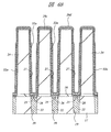
図示のように、メモリセルは、情報蓄積容量部である情報蓄積用容量素子Cをメモリセル選択用MISFETQsの上部に配置するスタックド・キャパシタ(Stacked capacitor)構造を採用している。情報蓄積用容量素子Cは、Ru(ルテニウム)を主成分として含む金属からなる下部電極(ストレージノード)28と、下部電極28の上部に形成されたTa2O5(酸化タンタル)を主成分として含む誘電体膜29と、誘電体膜29の上部に形成されたTiN(窒化チタン)を主成分として含む金属からなる上部電極(プレート電極)30とによって構成されている。この情報蓄積用容量素子Cは、メモリセル選択用MISFETQsの上部の厚い膜厚の酸化シリコン膜24に形成された高アスペクト比の溝27の内部に形成されている。
【0034】
情報蓄積用容量素子Cの下部電極28とメモリセル選択用MISFETQsのソース、ドレインの一方(n型半導体領域8)とは、コンタクトホール12およびその上部のスルーホール19を通じて電気的に接続されている。コンタクトホール12およびスルーホール19のそれぞれの内部には、多結晶シリコン膜からなるプラグ13、22が埋め込まれている。
【0035】
情報蓄積用容量素子Cの下部電極28とその下部のスルーホール19に埋め込まれたプラグ22との界面には、製造工程の途中で行われる熱処理によって、下部電極28を構成するRuとプラグ22を構成する多結晶シリコンとが不所望のシリサイド反応を引き起こすのを防ぐバリア層として、Ruシリサイド層25およびRuシリコンナイトライド層26が形成されている。上層のバリア層であるRuシリコンナイトライド層26は、製造工程の途中で行われる熱処理によって酸化され、少なくともその一部がRuシリコンオキシナイトライドとなっている場合もある。
【0036】
次に、本実施形態のDRAMの製造方法を図4〜図58を−用いて工程順に説明する。なお、以下で説明するDRAMの製造工程のうち、基板1の主面上にメモリセル選択用MISFETQsを形成し、続いてメモリセル選択用MISFETQsの上部にビット線BLを形成するまでの工程については、例えば特願平11−166320号(松岡ら)に詳細な記載がある。従って、本実施形態では、ビット線BLを形成するまでの工程についてはその概要を記載するに止め、主要な構成部分である情報蓄積用容量素子Cの製造工程について詳述する。また、ビット線BLを形成するまでの工程は、以下で説明する工程に限定されるものではない。
【0037】
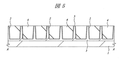
まず、図4(メモリアレイの要部平面図)、図5(図4のA−A線に沿った断面図)、図6(図4のB−B線に沿った断面図)および図7(図4のC−C線に沿った断面図)に示すように、例えばp型の単結晶シリコンからなる基板1の主面の素子分離領域に素子分離溝2を形成する。素子分離溝2は、基板1の表面をエッチングして深さ300〜400nm程度の溝を形成し、続いてこの溝の内部を含む基板1上にCVD(Chemical Vapor Deposition)法で酸化シリコン膜4(膜厚600nm程度)を堆積した後、酸化シリコン膜4を化学機械研磨(Chemical Mechanical Polishing;CMP)法で研磨、平坦化することによって形成する。酸化シリコン膜4は、例えば酸素(またはオゾン)とテトラエトキシシラン(TEOS)とをソースガスに用いたプラズマCVD法で堆積し、その後、1000℃程度のドライ酸化を行って膜を緻密化(デンシファイ)する。
【0038】
図4に示すように、素子分離溝2を形成することにより、この素子分離溝2によって周囲を囲まれた細長い島状の活性領域(L)が同時に多数形成される。後述するように、これらの活性領域(L)のそれぞれには、ソース、ドレインの一方を共有するメモリセル選択用MISFETQsが2個ずつ形成される。
【0039】
次に、基板1にB(ホウ素)をイオン打ち込みすることによってp型ウエル3を形成し、続いてp型ウエル3の表面をHF(フッ酸)系の洗浄液で洗浄した後、基板1を熱酸化することによってp型ウエル3の活性領域(L)の表面に酸化シリコン系の清浄なゲート絶縁膜5(膜厚6nm程度)を形成する。なお、ゲート絶縁膜5は、基板1の熱酸化によって形成される酸化シリコン系絶縁膜の他、それよりも誘電率が大きい窒化シリコン系絶縁膜、金属酸化物系絶縁膜(酸化タンタル膜、酸化チタン膜など)であってもよい。これらの高誘電体絶縁膜は、基板1上にCVD法やスパッタリング法で成膜することによって形成する。
【0040】
次に、図8〜図10に示すように、ゲート絶縁膜5の上部にゲート電極6を形成する。ゲート電極6は、活性領域(L)以外の領域ではワード線(WL)として機能する。ゲート電極6(ワード線WL)は、例えばゲート絶縁膜5の上部にP(リン)などをドープしたn型多結晶シリコン膜(膜厚70nm程度)、WN(窒化タングステン)またはTiN(窒化チタン)からなるバリアメタル膜(膜厚5nm〜10nm程度)、W(タングステン)膜(膜厚100nm程度)および窒化シリコン膜7(膜厚150nm程度)を順次堆積した後、フォトレジスト膜をマスクにしてこれらの膜をドライエッチングすることによって形成する。多結晶シリコン膜および窒化シリコン膜7はCVD法で堆積し、バリアメタル膜およびW膜はスパッタリング法で堆積する。
【0041】
次に、図11〜図13に示すように、p型ウエル3にAs(ヒ素)またはP(リン)をイオン打ち込みしてゲート電極6の両側のp型ウエル3にn型半導体領域8(ソース、ドレイン)を形成する。ここまでの工程により、メモリセル選択用MISFETQsが略完成する。
【0042】
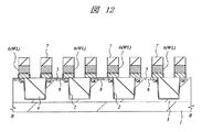
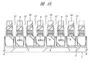
次に、図14〜図17に示すように、基板1上にCVD法で窒化シリコン膜9(膜厚50nm)および酸化シリコン膜10(膜厚600nm程度)を堆積し、続いて酸化シリコン膜10の表面を化学機械研磨法で平坦化した後、フォトレジスト膜(図示せず)をマスクにして酸化シリコン膜10および窒化シリコン膜9をドライエッチングすることにより、メモリセル選択用MISFETQsのソース、ドレイン(n型半導体領域8)の上部にコンタクトホール11、12を形成する。酸化シリコン膜10のエッチングは、窒化シリコンに対する選択比が大きい条件で行い、窒化シリコン膜9のエッチングは、シリコンや酸化シリコンに対するエッチング選択比が大きい条件で行う。これにより、コンタクトホール11、12をゲート電極6(ワード線WL)に対して自己整合(セルフアライン)で形成することができる。
【0043】
次に、図18および図19に示すように、コンタクトホール11、12の内部にプラグ13を形成する。プラグ13を形成するには、酸化シリコン膜10の上部にPをドープしたn型多結晶シリコン膜をCVD法で堆積することによってコンタクトホール11、12の内部にn型多結晶シリコン膜を埋め込んだ後、コンタクトホール11、12の外部のn型多結晶シリコン膜を化学機械研磨法(またはドライエッチング)で除去する。
【0044】
次に、酸化シリコン膜10の上部にCVD法で酸化シリコン膜14(膜厚150nm程度)を堆積した後、図20〜図22に示すように、フォトレジスト膜(図示せず)をマスクにしてコンタクトホール11の上部の酸化シリコン膜14をドライエッチングすることにより、後の工程で形成されるビット線(BL)とコンタクトホール11とを接続するためのスルーホール15を形成する。
【0045】
次に、図23および図24に示すように、スルーホール15の内部にプラグ16を形成する。プラグ16を形成するには、酸化シリコン膜14の上部に例えばスパッタリング法でTiNからなるバリアメタル膜を堆積し、続いてバリアメタル膜の上部にCVD法でW膜を堆積することによってスルーホール15の内部にこれらの膜を埋め込んだ後、スルーホール15の外部のこれらの膜を化学機械研磨法で除去する。
【0046】
次に、図25〜図28に示すように、酸化シリコン膜14の上部にビット線BLを形成する。ビット線BLを形成するには、例えば酸化シリコン膜14の上部にスパッタリング法でTiN膜(膜厚10nm程度)を堆積し、続いてTiN膜の上部にCVD法でW膜(膜厚50nm程度)を堆積した後、フォトレジスト膜をマスクにしてこれらの膜をドライエッチングする。ビット線BLは、その下部のスルーホール15に埋め込まれたプラグ16およびさらにその下部のコンタクトホール11に埋め込まれたプラグ13を介してメモリセル選択用MISFETQsのソース、ドレイン(n型半導体領域8)の一方と電気的に接続される。
【0047】
次に、図29〜図32に示すように、ビット線BLの上部にCVD法で膜厚300nm程度の酸化シリコン膜17を堆積し、続いて化学機械研磨法でその表面を平坦化した後、フォトレジスト膜(図示せず)をマスクにして酸化シリコン膜17をドライエッチングすることにより、プラグ13が埋め込まれたコンタクトホール11の上部にスルーホール19を形成する。
【0048】
スルーホール19は、その径がその下部のコンタクトホール11の径よりも小さくなるように形成する。具体的には、酸化シリコン膜17の上部にCVD法で多結晶シリコン膜20を堆積し、続いてスルーホール19を形成する領域の多結晶シリコン膜20をドライエッチングして孔を形成した後、多結晶シリコン膜20の上部にさらに多結晶シリコン膜(図示せず)を堆積する。次に、多結晶シリコン膜20の上部の多結晶シリコン膜を異方性エッチングすることによって孔の側壁にサイドウォールスペーサ21を形成し、続いて多結晶シリコン膜20とサイドウォールスペーサ21とをマスクに用いて孔の底部の酸化シリコン膜17をドライエッチングする。
【0049】
また、図29および図32に示すように、スルーホール19は、その中心がその下部のコンタクトホール11の中心よりもビット線BLから離れる方向にオフセットされる。このように、スルーホール19の径をその下部のコンタクトホール11の径よりも小さくし、かつその中心をビット線BLから離れる方向にオフセットさせることにより、メモリセルサイズを縮小した場合においても自己整合コンタクト(Self Align Contact;SAC)技術を用いることなく、スルーホール19(の内部に埋め込まれるプラグ22)とビット線BLとのショートを防止することができる。また、スルーホール19の径をその下部のコンタクトホール11の径よりも小さくすることにより、それらの中心をずらしても両者のコンタクト面積を十分に確保することができる。
【0050】
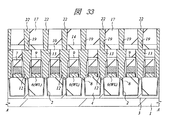
次に、スルーホール19の形成に用いたマスク(多結晶シリコン膜20およびサイドウォールスペーサ21)をドライエッチングで除去した後、図33〜図35に示すように、スルーホール19の内部にプラグ22を形成する。プラグ22を形成するには、まず酸化シリコン膜17の上部にPをドープしたn型多結晶シリコン膜をCVD法で堆積することによって、スルーホール19の内部にn型多結晶シリコン膜を埋め込み、続いてスルーホール19の外部のn型多結晶シリコン膜を化学機械研磨法(またはドライエッチング)で除去する。
【0051】
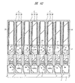
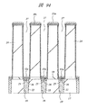
次に、図36および図37に示すように、酸化シリコン膜17の上部にCVD法で膜厚200nm程度の窒化シリコン膜18を堆積した後、窒化シリコン膜18の上部にCVD法で酸化シリコン膜24を堆積する。情報蓄積用容量素子Cの下部電極28は、次の工程で酸化シリコン膜24に形成される溝27の内部に形成される。従って、酸化シリコン膜24の膜厚がこの下部電極28の高さとなるので、下部電極28の表面積を大きくして蓄積電荷量を増やすためには、酸化シリコン膜24を厚い膜厚(0.8μm程度以上)で堆積する。酸化シリコン膜24は、例えば酸素とテトラエトキシシラン(TEOS)とをソースガスに用いたプラズマCVD法で堆積し、その後、必要に応じてその表面を化学機械研磨法で平坦化する。
【0052】
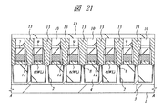
次に、図38〜図40に示すように、フォトレジスト膜(図示せず)をマスクにして酸化シリコン膜24をドライエッチングし、続いて酸化シリコン膜24の下層の窒化シリコン膜18をドライエッチングすることにより、その底部にスルーホール19内のプラグ22の表面が露出する溝27を形成する。図38に示すように、溝27は、ワード線WLの延在方向に長辺を有し、かつビット線BLの延在方向に短辺を有する矩形の平面パターンで構成される。
【0053】
溝27は、次のような方法で形成することもできる。まず、前述した方法で酸化シリコン膜17の上部に窒化シリコン膜18および厚い膜厚の酸化シリコン膜24を順次堆積し、続いて酸化シリコン膜24の上部にCVD法で窒化シリコン膜(図示せず)を堆積した後、フォトレジスト膜をマスクにしてこの窒化シリコン膜をドライエッチングする。次に、このフォトレジスト膜を除去した後、窒化シリコン膜をマスクにして酸化シリコン膜24をドライエッチングし、さらに窒化シリコン膜18をドライエッチングすることによって溝27を形成する。
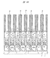
【0054】
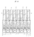
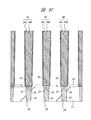
次に、図41および図42に示すように、深い溝27が形成された酸化シリコン膜24の上部にスパッタリング法でRu膜23を堆積する。このRu膜23は、溝27の底部でその膜厚が50nm程度となるような薄い膜厚で堆積する。一般に、スパッタリング法で堆積する膜は、CVD法で堆積する膜に比べて段差被覆性が低いため、深い溝27の側壁にはRu膜23が堆積し難い。図41および図42には、酸化シリコン膜24の上部と溝27の底部にRu膜23が堆積している状態を示したが、実際には溝27の側壁にも非常に薄い膜(図示せず)が堆積している。溝27の側壁に堆積したこの薄い膜は、後の工程で溝27の内部に堆積するCVD−Ru膜(Ru膜28a)の接着性を改善する効果がある。
【0055】
次に、図43および図44に示すように、窒素などの非酸化性ガス雰囲気中で700℃、1分程度の熱処理を行い、溝27の底部のRu膜23とその下部の多結晶シリコンからなるプラグ22とを反応させることによって、プラグ22の表面にRuシリサイド層25を形成する。このとき、酸化シリコン膜24の上部のRu膜23はシリサイド反応が生じないのでそのままの状態で残る。
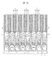
【0056】
上記Ruシリサイド層25は、後の工程で行われる熱処理、例えば後述する情報蓄積容量素子Cの誘電体膜形成工程で行われる高温熱処理の際などに、下部電極28を構成するRuとプラグ22を構成する多結晶シリコンとの界面で所望しないシリサイド反応が生じるのを防ぐと共に、接触抵抗を低減するために形成する。
【0057】
次に、図45および図46に示すように、アンモニアガス雰囲気中で650℃、3分程度の熱処理を行い、Ruシリサイド層25の表面を窒化することによってRuシリコンナイトライド層26を形成する。上記した熱処理条件によって形成されるRuシリコンナイトライド層26の膜厚は極めて薄く、本発明者が透過電子顕微鏡で観察した結果では、0.5nm〜1.0nmの範囲であった。
【0058】
Ruシリコンナイトライド層26の膜厚は、上記した熱処理条件を変えることによって制御することができる。すなわち、アンモニアガス雰囲気中で多結晶シリコン(プラグ22)の表面を窒化する場合、窒化反応は550℃程度から始まり、高温になる程反応が速く進行する。この窒化反応の特徴は、反応が自己整合的に停止することにあるため、Ruシリコンナイトライド層26の膜厚を極めて高精度に制御できるという利点がある。
【0059】
Ruシリコンナイトライド層26は、Ruシリサイド層25の上部にCVD法で窒化シリコン膜を堆積し、熱処理によって両者を反応させて形成することも考えられる。しかし、この方法では1nm程度の極めて薄い膜を制御性よく形成することは困難である。上記したアンモニアガス雰囲気中での熱処理(熱窒化法)では、1000℃程度の高温で熱処理を行っても、形成される膜厚は高々2nm程度であり、処理時間にはほとんど依存しない。処理時間が1分以上の場合は、温度の設定だけで膜厚をほぼ制御することができる。この熱窒化法では、形成された膜の内部を窒化剤が拡散し、シリコン表面に到達して窒化膜を形成するという過程を辿る。この窒化膜は極めて緻密なため、形成された膜自身が窒化剤の拡散を阻止する役割を果たす。従って、厚い膜を形成することはできないが、前記のような薄い膜厚のRuシリコンナイトライド層26を形成するには極めて都合のよい方法である。
【0060】
Ruシリコンナイトライド層26は、上記した熱窒化法に代え、プラズマ雰囲気中で生成する活性窒素を利用した窒化処理(プラズマ窒化法)によって形成してもよい。プラズマ窒化法においても窒化膜が形成される原理は熱窒化法と同じであるが、プラズマ中の活性窒素を窒化剤として用いるので、より低温で膜を形成することができるという利点があり、例えば膜厚1nm程度の窒化膜であれば300℃〜400℃の温度範囲で形成することができる。
【0061】
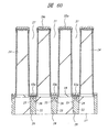
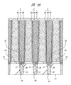
このように、本実施形態では、情報蓄積用容量素子Cの下部電極28を構成するRuとプラグ22を構成する多結晶シリコンとが不所望のシリサイド反応を引き起こすのを防ぐバリア層として、プラグ22の表面にRuシリサイド層25およびRuシリコンナイトライド層26を形成する。Ruシリコンナイトライド層26は、情報蓄積容量素子Cの誘電体膜形成工程で行われる酸素雰囲気中での高温熱処理の際、誘電体膜29中および下部電極28中を拡散した酸化剤(酸素)がRuシリサイド層25の表面を酸化し、誘電率の小さい酸化シリコン層(Ruシリコンオキサイド層)が形成されたり、極端な場合には下部電極28の形状異常が引き起こされたりする不具合を防ぐ機能がある。また、本実施形態ではこのRuシリコンナイトライド層26を熱窒化法(またはプラズマ窒化法)によって自己整合的に形成する。これにより、Ruシリコンナイトライド層26の膜厚を極めて薄くすることができるため、下部電極28とプラグ22との電気的導通が阻害されることもない。
【0062】
次に、図47および図48に示すように、酸化シリコン膜24の上部および溝27の内部にCVD法で膜厚10nm〜20nm程度の薄いRu膜28aを堆積する。Ru膜28aは、例えばRu(C2H5−C5H4)2(エチルシクロペンタジエニルルテニウム)と酸素とを原料ガスに用いた熱CVD法で堆積する。CVD法で堆積したRu膜28aは、スパッタリング法で堆積したRu膜23に比べて段差被覆性がよいため、図示のように、深い溝27の内部(底部および側壁)でほぼ均一な膜厚となる。CVD法で堆積したRu膜28aは、スパッタリング法で堆積したRu膜23に比べて酸化シリコン膜24との接着力は弱い。しかし、あらかじめその下層にスパッタリング法でRu膜23を堆積しておくことにより、溝27の内壁のRu膜28aが剥離する不具合を防ぐことができる。ただし前述したように、溝27の側壁に堆積したRu膜23は極めて薄いため、Ru膜28aの剥離を完全に防ぐことができない場合もある。これを防止するために、例えば図49および図50に示すように、あらかじめスパッタリング法で膜厚10nm〜20nm程度の薄いRu膜28bを堆積した後、その表面にCVD法でRu膜28aを堆積してもよい。
【0063】
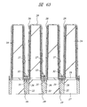
次に、図51および図52に示すように、溝27の内部に絶縁膜31を埋め込み、絶縁膜31で覆われていない溝27の外部のRu膜28a、23をドライエッチングによって除去する。絶縁膜31は、酸化シリコン膜24に対するエッチング選択比が大きい絶縁材料、例えばフォトレジストやスピンオングラスなどで構成する。絶縁膜31をフォトレジストで構成した場合は、ポジ型のフォトレジスト膜を溝27の内部および酸化シリコン膜24上にスピン塗布した後、全面露光および現像を行って溝27の外部の露光部を除去し、溝27の内部に未露光部を残せばよい。
【0064】
次に、図53および図54に示すように、溝27の内部の絶縁膜31を除去する。絶縁膜31をフォトレジストで構成した場合には、酸素ラジカルによるアッシング処理を行うことによって絶縁膜31を除去することができる。また、この段階でRu膜28aの緻密化を図るため、真空中で700℃、1分程度の熱処理を行う。これにより、溝27の内壁に堆積したRu膜28aからなる下部電極28が得られる。この下部電極28は、その下部のスルーホール19に埋め込まれたプラグ22およびさらにその下部のコンタクトホール12に埋め込まれたプラグ13を介してメモリセル選択用MISFETQsのn型半導体領域8(ソース、ドレイン)の他方と電気的に接続される。
【0065】
次に、図55および図56に示すように、下部電極28が形成された溝27の内壁および酸化シリコン膜24の表面に酸化タンタルからなる誘電体膜29を薄く堆積する。酸化タンタル膜は、例えば原料ガスにペンタエトキシタンタル(Ta(OC2H5)5)と酸素とを用い、温度430℃、圧力50Paの条件で堆積し、その後、膜の結晶化と膜質の改善とを図るために、酸素雰囲気中で熱処理を行う。
【0066】
特に限定はされないが、本実施形態では下部電極28と接する部分の酸化タンタル膜の結晶化と膜質の改善とを効果的に実施するために、成膜と熱処理とを2回ずつ行う。具体的には、ホットウォール型の枚葉式CVD装置を使用して最初に5nmの酸化タンタル膜を堆積し、続いてRTA(Rapid Thermal Anneal)装置を使用して酸素雰囲気中、650℃、1分の熱処理を行った後、さらにこれらの装置を使用して5nmの酸化タンタル膜を堆積し、酸素雰囲気中、600℃、2分の熱処理を行う。
【0067】
酸化タンタル膜の成膜と熱処理とを2回ずつ行う場合は、最初の成膜後の熱処理条件が重要であり、最初の熱処理で酸化タンタル膜の結晶化を完結させる必要がある。この熱処理で酸化タンタル膜が結晶化していれば、2回目の成膜で形成した酸化タンタル膜は成膜完了時にすでに結晶化が完結している(ホモエピタキシャル成長)ので、2回目の熱処理は必ずしも必要ではない。このホモエピタキシャル成長は、酸化タンタルに限らず、CVD法で成膜する金属酸化物には、程度の差はあるものの共通する現象である。但し、よりリーク電流の少ない酸化タンタル膜を得るためには、2回目の熱処理を行った方がよい。
【0068】
上記熱処理を施すことにより、プラグ22の表面に形成されたRuシリコンナイトライド層26が酸化され、少なくともその一部は、Ruシリコンオキシナイトライドに変化する。すなわち、誘電体膜29を構成する酸化タンタル膜を酸素雰囲気中で高温熱処理すると、酸化タンタル膜および下部電極28を透過、拡散した酸素がRuシリコンナイトライド層26に達し、少なくともその一部が酸化されてRuシリコンオキシナイトライドとなる場合がある。これにより、Ruシリコンナイトライド層26またはRuシリコンオキシナイトライドが酸素拡散のバリア層となるため、Ruシリコンナイトライド層26の下層のRuシリサイド層25が上記酸素によって酸化されてプラグ22の表面に導電率の小さい酸化シリコン層(Ruシリコンオキサイド層)が形成されたり、下部電極28の形状異常を引き起こしたりする不具合を防止することができる。
【0069】
本実施形態では、誘電体膜29を構成する酸化タンタル膜の結晶化および膜質の改善のための熱処理を650℃で行うが、このような低い熱処理温度での結晶化および膜質の改善は、酸化タンタル膜の下地である下部電極28をRu膜で構成した場合に特徴的なものである。例えば酸化シリコンなどの絶縁膜上に堆積した酸化タンタル膜の結晶化および膜質の改善を行うためには、実用上750℃以上の高温熱処理が必要となるが、酸化タンタル膜の下地である下部電極28がRu膜で構成されている場合には、100℃以上も低い温度の熱処理で済む。これは、製造工程全体の熱処理量を低減する上で極めて大きい利点となる。
【0070】
次に、図57および図58に示すように、誘電体膜29の上部に上部電極30を形成する。上部電極30を形成するには、まずCVD法で堆積したTiN膜で溝27の内部を埋め込み、続いてその上部にスパッタリング法でTiN膜を堆積した後、メモリアレイ(MARY)領域以外の不要なTiN膜と誘電体膜29とをエッチングで除去する。
【0071】
なお、溝27の内部はCVD法で堆積したTiN膜で完全に埋め込む必要はない。CVD法で堆積したTiN膜は、少なくとも誘電体膜29の表面全体を覆っていればよく、その後、スパッタリング法で堆積したTiN膜で溝27の内部を完全に覆うようにしてもよい。また、上部電極材料として、Ru膜とTiN膜との積層膜やRu膜とW膜との積層膜などを使用することもできる。
【0072】
ここまでの工程により、下部電極28、誘電体膜29および上部電極30によって構成される情報蓄積用容量素子Cが完成し、前記図2および図3に示したような、メモリセル選択用MISFETQsとこれに直列に接続された情報蓄積容量素子Cとで構成されるメモリセルが略完成する。
【0073】
その後、情報蓄積用容量素子Cの上部に層間絶縁膜を挟んで2層程度のAl配線を形成し、最上層のAl配線の上部にパッシベーション膜を形成するが、これらの図示は省略する。
【0074】
以上詳述したように、本実施形態によれば、情報蓄積用容量素子Cの下部電極28に接続されたプラグ22の表面にRuシリサイド層25を形成し、さらにRuシリサイド層25の表面にRuシリコンナイトライド層26を形成することにより、下部電極28上に誘電体膜29を形成する工程で行われる酸素雰囲気中での高温熱処理の際、Ruシリサイド層25またはRuシリコンナイトライド層26が酸化されることによって形成されたRuシリコンオキシナイトライドが酸素バリアとなるため、Ruシリサイド層25の酸化の進行を有効に防止することができる。これにより、下部電極28とプラグ22との界面の異常酸化に起因する下部電極28の形状不良の発生を防止できるので、下部電極28上に形成される誘電体膜29のリーク電流を減少させることができる。
【0075】
なお、本実施形態では、溝27が形成された酸化シリコン膜24の上部にRu膜23を堆積し、続いて熱処理を行うことによってプラグ22の表面にRuシリサイド層25を形成したが、このRu膜23はスパッタリング法で堆積するので溝27の側壁にはほとんど堆積しない。しかし、微視的には溝27の側壁にも僅かながら堆積しており、これがその後の工程でCVD法により堆積するRu膜28aのシード層として機能し、Ru膜28と酸化シリコン膜24との接着力を向上させる。このシード層は、Ru膜に限定されるものではないが、一般に酸化シリコンなどの絶縁膜上にCVD法でRu膜を堆積する場合には、金属材料からなるなんらかのシード層を形成することが、Ru膜の剥離を防止する上で有効である。
【0076】
また、本実施形態の製造方法では、スルーホール19に多結晶シリコンのプラグ22を埋め込み、続いてその上部に酸化シリコン膜24を堆積して溝27を形成した後、溝27の底部に露出したプラグ22の表面にRuシリサイド層25およびRuシリコンナイトライド層26を形成する。これにより、Ruシリサイド層25およびRuシリコンナイトライド層26が溝27に対して自己整合的に形成されるので、スルーホール19と溝27との合わせずれが生じた場合でも、情報蓄積用容量素子Cの誘電体膜29とプラグ22との接触を回避することができ、情報蓄積用容量素子Cのリーク電流の増加を抑えることができる。
【0077】
プラグ22の表面に形成するシリサイド層は、Ruシリサイドに限定されるものではなく、例えばPt(プラチナ)シリサイド、Ti(チタン)シリサイド、Co(コバルト)シリサイドなどで構成することもできる。
【0078】
また、下部電極材料はRuに限定されるものではなく、例えばPt、Ir(イリジウム)などで構成することもできる。本実施形態で使用したRuは、過剰な酸化性雰囲気中で熱処理した場合、Ru自身が酸化されて酸化ルテニウムを形成し、後の工程で不都合を生じる場合があるが、Ptはこのような酸化物を形成しないという利点がある。
【0079】
また、情報蓄積用容量素子Cの上部電極材料はTiNに限定されるものではなく、例えばW、Ru、Pt、Irなどの金属またはこれらの金属とTiNとを積層したものなどで構成することもできる。
【0080】
(実施の形態2)
本実施形態の製造方法は、プラグ22の表面にRuシリサイド層25を形成し、続いてRuシリサイド層25の表面にRuシリコンナイトライド層26を形成するまでの工程(前記図4〜図46の工程)が前記実施の形態1と同一であるため、その説明は省略し、以降の工程についてのみ説明する。
【0081】
まず、前記図46に示した工程に引き続き、図59に示すように、酸化シリコン膜24の上部および溝27の内部に段差被覆性のよいCVD法で薄いRu膜28cを堆積する。このRu膜28cは、前記実施の形態1のRu膜28aに相当するものであるが、その膜厚は、Ru膜28aの半分程度(5nm〜10nm程度)とする。前述したように、CVD法で堆積したRu膜28cは、スパッタリング法で堆積したRu膜に比べて段差被覆性はよいが、酸化シリコン膜24との接着力は弱い。従って、前記実施の形態1と同様、Ru膜28cを堆積する工程に先立って、スパッタリング法で薄いRu膜(図示せず)を堆積してもよい。
【0082】
次に、図60に示すように、Ru膜28cの上部にスパッタリング法で膜厚10nm〜20nm程度のWシリサイド膜32aを堆積する。Wシリサイド膜32aはスパッタリング法で堆積するので、溝27の外部の酸化シリコン膜24上や溝27の底部には堆積しても、溝27の側壁には極く薄い膜厚でしか堆積しない。他方、溝27の側壁にWシリサイド膜32aが堆積すると、次の工程で薄いRu膜28dを堆積したときにその一部(Ru膜28dの膜厚が薄くなった箇所)でWシリサイド膜32aが露出することがある。このような現象が生じると、後の工程で堆積する誘電体膜29とWシリサイド膜32aとが接触し、誘電体膜29の特性が劣化する虞れがある。このような虞れがある場合は、Wシリサイド膜32aを堆積した後、溝27の側壁、特に側壁上端部の薄いWシリサイド膜32aをドライエッチング処理やウェットエッチング処理によって除去しておくことが望ましい。また、Wシリサイド膜32aの膜厚が溝27の側壁よりも底部で厚いことを利用し、エッチング時間を制御することによって溝27の底部のみにWシリサイド膜32aを残したり、溝27の底部にフォトレジスト膜などの絶縁膜を埋め込み、この絶縁膜で覆われていない側壁上端部のWシリサイド膜32aのみをエッチングで除去したりしてもよい。
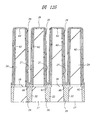
【0083】
次に、図61に示すように、Wシリサイド膜32aの上部に段差被覆性のよいCVD法で膜厚5nm〜10nm程度の薄いRu膜28dを堆積する。ここまでの工程で酸化シリコン膜24の上部および溝27の内壁にRu膜28c、28dが堆積され、かつ酸化シリコン膜24の上部および溝27の底部には、Ru膜28c、28dに挟まれた状態でWシリサイド膜32aが残留する。
【0084】
次に、図62に示すように、溝27の外部のRu膜28c、28d、23およびWシリサイド膜32aをドライエッチングによって除去する。これにより、溝27の内壁には2層のRu膜28c、28dからなる下部電極28が形成され、溝27の底部の下部電極28内にはWシリサイド膜32aからなる酸素吸収層32が形成される。溝27の外部のRu膜28c、28d、23およびWシリサイド膜32aを除去するには、前記実施の形態1と同様、溝27の内部にフォトレジストやスピンオングラスなどの絶縁膜31を埋め込んでドライエッチングを行えばよい。
【0085】
次に、図63に示すように、下部電極28が形成された溝27の内壁および酸化シリコン膜24の表面に誘電体膜29を薄く堆積する。誘電体膜29は、膜厚10nm程度の酸化タンタル(Ta2O5)膜で構成し、その後、膜の結晶化と膜質の改善とを図るために、酸素雰囲気中で600℃程度の熱処理を行う。この熱処理を施すことにより、プラグ22の表面に形成されたRuシリコンナイトライド層26が酸化され、少なくともその一部がRuシリコンオキシナイトライドに変化する場合もある。
【0086】
次に、図64に示すように、CVD法とスパッタリング法とを組み合わせて誘電体膜29の上部にTiN膜を堆積して上部電極30を形成することにより、下部電極28、誘電体膜29および上部電極30によって構成される情報蓄積用容量素子Cが完成し、メモリセル選択用MISFETQsとこれに直列に接続された情報蓄積容量素子Cとで構成されるメモリセルが略完成する。
【0087】
このように、本実施形態ではプラグ22の表面にRuシリサイド層25を形成し、Ruシリサイド層25の表面にRuシリコンナイトライド層26を形成した後、溝27の底部の下部電極28内に酸素吸収層32を形成する。これにより、下部電極28上に誘電体膜29を形成する工程で行われる酸素雰囲気中での高温熱処理の際、Ruシリコンナイトライド層26および酸素吸収層32が下部電極28中を透過、拡散する酸素のバリア層として機能し、犠牲的に酸化されるため、前記実施の形態1に比べてRuシリサイド層25の酸化の進行をより効果的に防止することができる。
【0088】
上記酸素吸収層32は、下部電極28を構成する2層のRu膜28c、28dに挟み込まれた状態で形成される。そのため、酸素吸収層32が酸化されることによってその導電性が失われた場合でも、その外側のRu膜28cによって下部電極28とプラグ22との導通が確保されるため、情報蓄積用容量素子C全体の機能および特性が劣化することはない。
【0089】
酸素吸収層32を構成する導電材料はWシリサイドに限定されるものではないが、下部電極28を構成する2層のRu膜28c、28dに挟み込まれた状態で形成されるため、高温熱処理の際に大きな体積変化を伴う材料は、誘電体膜29に歪みを発生させてその特性を劣化させる虞れがあるので好ましくない。
【0090】
例えばW、Tiなどの純金属は、酸素を吸収する導電材料としては理想的であるが、酸化によって体積変化を伴うので、酸素吸収層32として使用する場合には、その膜厚を5nm以下にすることが望ましい。また、シリコンも良好な酸素吸収材であるが、酸化によって体積変化を伴うので、酸素吸収層32として使用する場合には、その膜厚を5nm以下にすることが望ましい。さらに、Al(アルミニウム)を使用することも可能であるが、融点が約660℃と低いため、誘電体膜29の熱処理を融点以下の低温で行える場合に限られる。
【0091】
酸素吸収層32を構成する導電材料として最も好ましいのは、その成膜段階または誘電体膜29の形成直前においてシリサイド化が完結している金属シリサイドであり、具体的には本実施形態で用いたWシリサイドの他、Tiシリサイド、Ruシリサイド、Coシリサイドなどを例示することができる。その他、TaN(窒化タンタル)などの窒化金属を使用することもできる。
【0092】
(実施の形態3)
前記実施の形態2は、酸素吸収層32を溝27の底部に形成したが、本実施形態は、酸素吸収層32を溝27の底部と側壁とに形成する。
【0093】
まず、前記図46に示した工程に引き続き、図65に示すように、酸化シリコン膜24の上部および溝27の内部にCVD法で膜厚5nm〜10nm程度のRu膜28cを堆積する。なお、Ru膜28cの接着性を確保するために、あらかじめスパッタリング法でRu膜(図示せず)を堆積してからRu膜28cを堆積してもよい。
【0094】
次に、図66に示すように、Ru膜28cの上部にCVD法で膜厚10nm〜20nm程度のWシリサイド膜32bを堆積する。このWシリサイド膜32bはCVD法で堆積するので、溝27の外部の酸化シリコン膜24の上部、溝27の底部および側壁にほぼ均一な膜厚で堆積する。
【0095】
次に、図67に示すように、溝27の内部にフォトレジストやスピンオングラスなどからなる絶縁膜33を埋め込み、絶縁膜33で覆われていない溝27の外部のWシリサイド膜32bをドライエッチングによって除去する。このとき、Wシリサイド膜32bと後の工程で堆積する誘電体膜29との接触を避けるために絶縁膜31の上端部を溝27の開孔部よりも下方に後退させ、溝27の側壁上端部近傍のWシリサイド膜32bを同時に除去する。
【0096】
次に、溝27の内部の絶縁膜33を除去した後、図68に示すように、Wシリサイド膜32bの上部にCVD法で膜厚5nm〜10nm程度の薄いRu膜28dを堆積し、続いて図69に示すように、溝27の外部のRu膜28d、28c、23をドライエッチングによって除去する。これにより、溝27の内壁には2層のRu膜28c、28dからなる下部電極28が形成され、溝27の底部およ側壁の下部電極28内にはWシリサイド膜32aからなる酸素吸収層32が形成される。
【0097】
次に、図70に示すように、下部電極28が形成された溝27の内壁および酸化シリコン膜24の表面に誘電体膜29を薄く堆積する。誘電体膜29は、膜厚10nm程度の酸化タンタル膜で構成し、その後、膜の結晶化と膜質の改善とを図るために、酸素雰囲気中で650℃、2分程度の熱処理を行う。このとき、プラグ22の表面に形成されたRuシリコンナイトライド層26が酸化され、少なくともその一部がRuシリコンオキシナイトライドに変化する場合もある。
【0098】
次に、図71に示すように、CVD法とスパッタリング法とを組み合わせて誘電体膜29の上部にTiN膜などを堆積して上部電極30を形成することにより、下部電極28、誘電体膜29および上部電極30によって構成される情報蓄積用容量素子Cが完成し、メモリセル選択用MISFETQsとこれに直列に接続された情報蓄積容量素子Cとで構成されるメモリセルが略完成する。
【0099】
本実施形態では、酸素吸収層32を溝27の底部だけでなく側壁にも形成するため、溝27の底部のみに酸素吸収層32を形成する前記実施の形態2に比べて酸素吸収層32のバリア効果が大きく、Ruシリサイド層25の酸化の進行をより効果的に防止することができる。
【0100】
上記酸素吸収層32は、下部電極28を構成する2層のRu膜28c、28dに挟み込まれた状態で形成される。そのため、前記実施の形態2と同様、酸素吸収層32が酸化されることによってその導電性が失われた場合でも、その外側のRu膜28cによって下部電極28とプラグ22との導通が確保されるため、情報蓄積用容量素子C全体の機能および特性が劣化することはない。
【0101】
酸素吸収層32を構成する導電材料はWシリサイドに限定されるものではなく、前記実施の形態2で例示した各種導電材料を使用することができる。また、これらの導電材料に変えてシリコンを使用することもできる。
【0102】
酸素吸収層32をシリコンで構成する場合は、酸化シリコン膜24の上部および溝27の内部にRu膜28cを堆積(図65参照)した後、Ru膜28cの上部にCVD法で多結晶シリコン膜などを堆積する。次に、溝27の外部の多結晶シリコン膜をドライエッチングによって除去した後、熱処理を施してRu膜28cと多結晶シリコン膜とを反応させ、多結晶シリコン膜をシリサイド化することによって溝27の内部にRuシリサイド膜を形成する。その後、Ru膜28dを堆積し、続いて溝27の外部のRu膜28d、28c、23をドライエッチングによって除去することにより、溝27の内壁には2層のRu膜28c、28dからなる下部電極28が形成され、溝27の底部およ側壁の下部電極28内にはRuシリサイド膜からなる酸素吸収層32が形成される。
【0103】
上記のように、シリコンをシリサイド化して酸素吸収層32を形成する場合には、最初に堆積するRu膜28cの膜厚を多結晶シリコン膜の膜厚の2倍以上とする。例えばRu膜28cの膜厚を20nm、多結晶シリコン膜の膜厚を5nmとし、熱処理によって両者を反応させた場合、多結晶シリコン膜がすべてシリサイド化されてもRu膜がシリサイド化されるのは高々5nm程度であり、残り15nmは金属Ruとして残存するため、下部電極28の導通を十分に確保することができる。
【0104】
(実施の形態4)
前記実施の形態1〜3は、下部電極28の下部のスルーホール19に埋め込むプラグ22を多結晶シリコンで構成したが、本実施形態はスルーホール19に埋め込むプラグをRuで構成する。
【0105】
まず、図72に示すように、ビット線BLの上部に堆積した酸化シリコン膜17をドライエッチングすることによって、スルーホール19を形成する。ここまでの工程は、前記実施の形態1の図4〜図32に示す工程と同じである。
【0106】
次に、図73に示すように、スルーホール19が形成された酸化シリコン膜17の上部にスパッタリング法でRu膜34を堆積する。このRu膜23は、スルーホール19の底部でその膜厚が50nm程度となるような薄い膜厚で堆積する。なお、図には、酸化シリコン膜17の上部とスルーホール19の底部にRu膜34が堆積した状態を示しているが、実際にはスルーホール19の側壁にも非常に薄いRu膜34が堆積している。
【0107】
次に、図74に示すように、窒素などの非酸化性ガス雰囲気中で600℃、1分程度の熱処理を行い、スルーホール19の底部のRu膜34とその下部のコンタクトホール12に埋め込まれた多結晶シリコンからなるプラグ13とを反応させることによって、プラグ13の表面にRuシリサイド層35を形成する。このとき、酸化シリコン膜17の上部のRu膜34はシリサイド反応が生じないのでそのままの状態で残る。
【0108】
次に、図75に示すように、アンモニアガス雰囲気中で650℃、3分程度の熱処理(熱窒化処理)を行い、Ruシリサイド層35の表面を窒化することによってRuシリコンナイトライド層36を形成する。Ruシリコンナイトライド層36は、上記した熱窒化処理に代え、プラズマ雰囲気中で生成する活性窒素を利用した窒化処理(プラズマ窒化処理)によって形成してもよい。
【0109】
次に、図76に示すように、酸化シリコン膜17の上部およびスルーホール19の内部にCVD法でRu膜37aを堆積した後、図77に示すように、スルーホール19の外部のRu膜37aを化学機械研磨法(またはエッチバック)で除去することにより、スルーホール19の内部にRu膜37aからなるプラグ37を形成する。CVD法で堆積したRu膜37aは、スパッタリング法で堆積したRu膜に比べて酸化シリコン膜17との接着力が弱いため、あらかじめその下層にスパッタリング法でRu膜(図示せず)を堆積した後にRu膜37aを堆積してもよい。
【0110】
次に、図78に示すように、酸化シリコン膜17の上部にCVD法で窒化シリコン膜18および酸化シリコン膜24を堆積した後、フォトレジスト膜(図示せず)をマスクにして酸化シリコン膜24および窒化シリコン膜18をドライエッチングすることにより、その底部にスルーホール19内のプラグ37の表面が露出する溝27を形成する。
【0111】
次に、図79に示すように、前記実施の形態1の図47〜図54に示す工程に従い、溝27の内壁に沿ってRu膜からなる下部電極28を形成した後、図80に示すように、下部電極28が形成された溝27の内壁および酸化シリコン膜24の表面に誘電体膜29を薄く堆積する。誘電体膜29は、膜厚10nm程度の酸化タンタル(Ta2O5)膜で構成し、その後、膜の結晶化と膜質の改善とを図るために、酸素雰囲気中で650℃、2分程度の熱処理を行う。
【0112】
次に、図81に示すように、CVD法とスパッタリング法とを組み合わせて誘電体膜29の上部に窒化チタン膜を堆積して上部電極30を形成することにより、下部電極28、誘電体膜29および上部電極30によって構成される情報蓄積用容量素子Cが完成し、メモリセル選択用MISFETQsとこれに直列に接続された情報蓄積容量素子Cとで構成されるメモリセルが略完成する。
【0113】
このように、本実施形態ではスルーホール19の下部のコンタクトホール12に埋め込まれた多結晶シリコンからなるプラグ13の表面にRuシリサイド層35を形成し、このRuシリサイド層35の表面にRuシリコンナイトライド層36を形成する。また、コンタクトホール12の上部のスルーホール19にRu膜37aからなるプラグ37を埋め込む。
【0114】
本実施形態によれば、プラグ13の表面に形成したRuシリサイド層35およびRuシリコンナイトライド層36と情報蓄積用容量素子Cの誘電体膜29とがスルーホール19内のRu膜37aからなるプラグ37によって隔絶されるため、誘電体膜29を形成する工程で行われる酸素雰囲気中での高温熱処理の際、酸素の拡散によるRuシリサイド層35の酸化を効果的に防止することができる。
【0115】
本実施形態ではプラグ13の表面にRuシリサイド層35とRuシリコンナイトライド層36とを形成したが、これに限定されるものではなく、例えばTiシリサイド層とTiシリコンナイトライド層、あるいはCoシリサイド層とCoシリコンナイトライド層などを形成しても同様の効果が得られる。
【0116】
また、前記実施の形態2、3のように、下部電極28の間に酸素吸収層32を挟み込んだり、図82に示すように、Ru膜37aからなるプラグ37が埋め込まれたスルーホール19の内部に酸素吸収層32を形成したりしてもよい。
【0117】
また、スルーホール19内のプラグ37は、Ru膜37aに限定されるものではなく、例えばPtやIrなどを使用することもできる。
【0118】
(実施の形態5)
前記実施の形態1〜4のDRAMは、酸化シリコン膜24に形成した溝27の内壁に情報蓄積用容量素子Cの下部電極28を形成したが、本実施形態のDRAMは、情報蓄積用容量素子Cの下部電極を柱状に形成する。
【0119】
本実施形態の製造方法は、プラグ22の表面にRuシリサイド層25を形成し、続いてRuシリサイド層25の表面にRuシリコンナイトライド層26を形成するまでの工程(前記図4〜図46の工程)が前記実施の形態1と同一であるため、その説明は省略し、以降の工程についてのみ説明する。
【0120】
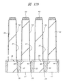
まず、前記図46に示した工程に引き続き、図83および図84に示すように、酸化シリコン膜24の上部および溝27の内部に段差被覆性のよいCVD法でRu膜38aを堆積する。このRu膜38aは、溝27の内部を完全に埋め込むような厚い膜厚で堆積する。
【0121】
次に、図85および図86に示すように、溝27の外部のRu膜38a、23をドライエッチングによって除去し、溝27の内部にRu膜38aを残した後、図87および図88に示すように、例えばフッ酸系のエッチング液を用いたウェットエッチングで酸化シリコン膜24を除去することにより、Ru膜38aからなる柱状の下部電極38を形成する。
【0122】
次に、図89および図90に示すように、下部電極38の表面に誘電体膜39を薄く堆積する。誘電体膜39は、膜厚10nm程度の酸化タンタル膜で構成し、その後、膜の結晶化と膜質の改善とを図るために、酸素雰囲気中で650℃、2分程度の熱処理を行う。
【0123】
次に、図91および図92に示すように、CVD法とスパッタリング法とを組み合わせて誘電体膜39の上部にTiN膜などを堆積して上部電極40を形成することにより、下部電極38、誘電体膜39および上部電極40によって構成される情報蓄積用容量素子Cが完成し、メモリセル選択用MISFETQsとこれに直列に接続された情報蓄積容量素子Cとで構成されるメモリセルが略完成する。
【0124】
このように、本実施形態によれば、情報蓄積用容量素子Cの下部電極28を柱状体で構成した場合においても、下部電極28に接続されたプラグ22の表面にRuシリサイド層25を形成し、さらにRuシリサイド層25の表面にRuシリコンナイトライド層26を形成することにより、下部電極28上に誘電体膜29を形成する工程で行われる酸素雰囲気中での高温熱処理の際、Ruシリコンナイトライド層26が犠牲的に酸化されてRuシリコンオキシナイトライドとなるため、Ruシリサイド層25の酸化の進行を有効に防止することができる。これにより、下部電極28とプラグ22との界面の異常酸化に起因する下部電極28の形状不良の発生を防止できるので、下部電極28上に形成される誘電体膜29のリーク電流を減少させることができる。
【0125】
また、本実施形態の製造方法では、スルーホール19に多結晶シリコンのプラグ22を埋め込み、続いてその上部に酸化シリコン膜24を堆積して溝27を形成した後、溝27の底部に露出したプラグ22の表面にRuシリサイド層25およびRuシリコンナイトライド層26を形成する。これにより、Ruシリサイド層25およびRuシリコンナイトライド層26が溝27に対して自己整合的に形成されるので、溝27によってその領域が規定される柱状の下部電極28とスルーホール19との合わせずれが生じた場合でも、誘電体膜29とプラグ22との接触を回避することができ、情報蓄積用容量素子Cのリーク電流の増加を抑えることができる。
【0126】
また、情報蓄積用容量素子Cの下部電極38を柱状体で構成する本実施形態によれば、下部電極28を溝27の内部に形成する前記実施の形態1〜4に比べ、下部電極38の上部に堆積する誘電体材料(酸化タンタル膜)および上部電極材料(TiN膜)の段差被覆性を向上させることができる。
【0127】
(実施の形態6)
本実施形態のDRAMは、前記実施の形態5と同じく情報蓄積用容量素子Cの下部電極を柱状体で構成し、かつ前記実施の形態2と同じく下部電極の底部に酸素吸収層を形成する。
【0128】
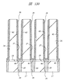
まず、前記図46に示した工程に引き続き、図93に示すように、酸化シリコン膜24の上部および溝27の内部に段差被覆性のよいCVD法で薄いRu膜38cを堆積する。前述したように、CVD法で堆積したRu膜38cは、スパッタリング法で堆積したRu膜に比べて段差被覆性はよいが、酸化シリコン膜24との接着力は弱いので、スパッタリング法で薄いRu膜(図示せず)を堆積した後にRu膜38cを堆積してもよい。
【0129】
次に、図94に示すように、Ru膜38cの上部にスパッタリング法で膜厚10nm〜20nm程度のWシリサイド膜32aを堆積する。このWシリサイド膜32aはスパッタリング法で堆積するので、溝27の外部の酸化シリコン膜24上や溝27の底部には堆積しても、溝27の側壁には極く薄い膜厚でしか堆積しない。
【0130】
次に、図95に示すように、Wシリサイド膜32aが堆積された酸化シリコン膜24の上部および溝27の内部に段差被覆性のよいCVD法でRu膜38dを堆積する。このRu膜38dは、溝27の内部を完全に埋め込むような厚い膜厚で堆積する。
【0131】
次に、図96に示すように、溝27の外部のRu膜38c、38dおよびWシリサイド膜32aをドライエッチングによって除去し、溝27の内部にRu膜38c、38dおよびWシリサイド膜32aを残した後、図97に示すように、例えばフッ酸系のエッチング液を用いたウェットエッチングで酸化シリコン膜24を除去することにより、Ru膜38aからなる柱状の下部電極38を形成し、下部電極38の底部にWシリサイド膜32aからなる酸素吸収層32を形成する。
【0132】
次に、図98に示すように、前記実施の形態5と同様の方法で下部電極38の表面に誘電体膜39を薄く堆積し、続いて酸素雰囲気中で熱処理を行った後、誘電体膜39の上部にTiN膜などを堆積して上部電極40を形成する。
【0133】
このように、本実施形態ではプラグ22の表面にRuシリサイド層25を形成し、Ruシリサイド層25の表面にRuシリコンナイトライド層26を形成した後、柱状の下部電極28の底部に酸素吸収層32を形成する。これにより、下部電極28上に誘電体膜29を形成する工程で行われる酸素雰囲気中での高温熱処理の際、Ruシリコンナイトライド層26および酸素吸収層32が下部電極28中を透過、拡散する酸素のバリア層として機能し、犠牲的に酸化されるため、前記実施の形態5に比べてRuシリサイド層25の酸化の進行をより効果的に防止することができる。
【0134】
(実施の形態7)
本実施形態のDRAMは、前記実施の形態5、6と同じく情報蓄積用容量素子Cの下部電極を柱状体で構成し、かつ下部電極の内部に酸素吸収層を形成する。
【0135】
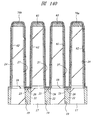
まず、前記図46に示した工程に引き続き、図99に示すように、酸化シリコン膜24の上部および溝27の内部に段差被覆性のよいCVD法でRu膜38eを堆積する。Ru膜38eは、溝27の内部を完全に埋め込まない程度の膜厚で堆積する。この場合も、あらかじめスパッタリング法で薄いRu膜(図示せず)を堆積してからRu膜38eを堆積してもよい。
【0136】
次に、図100に示すように、溝27の内部に多結晶シリコン膜50を埋め込む。多結晶シリコン膜50の埋め込みは、まずRu膜38eが堆積された酸化シリコン膜24の上部および溝27の内部にCVD法で多結晶シリコン膜50を堆積した後、溝27の外部の多結晶シリコン膜50をドライエッチングで除去する。このとき、溝27の上端部近傍の多結晶シリコン膜50をオーバーエッチングによって除去し、多結晶シリコン膜50の上面を溝27の上端部よりも下方に後退させる。
【0137】
次に、図101に示すように、窒素などの非酸化性ガス雰囲気中で熱処理を行い、溝27の内部のRu膜38eと多結晶シリコン膜50とを反応させてRuシリサイド膜を形成することにより、溝27の内部にRuシリサイドからなる酸素吸収層51を形成する。
【0138】
多結晶シリコン膜50をシリサイド化して酸素吸収層51を形成する場合は、前述したように、最初に堆積するRu膜28eの膜厚を多結晶シリコン膜50の膜厚の2倍以上とする。例えば溝27の径を100nmとし、Ru膜28eの膜厚を30nmとした場合、溝27の両側壁に堆積するRu膜28eの膜厚は60nmとなるため、その後に溝27の内部に埋め込まれる多結晶シリコン膜50の横方向の膜厚は40nmとなる。この膜厚比でRu膜28eと多結晶シリコン膜50とを反応させた場合、多結晶シリコン膜50がすべてシリサイド化されてもRu膜28eがシリサイド化されるのは10nm程度であり、残り20nmは金属Ruとして残存するため、下部電極38の導通を十分に確保することができる。
【0139】
次に、図102に示すように、酸化シリコン膜24の上部および酸素吸収層51が形成された溝27の内部にCVD法でRu膜38fを堆積する。このRu膜38fは、溝27の内部を完全に埋め込むような厚い膜厚で堆積する。
【0140】
次に、図103に示すように、溝27の外部のRu膜38f、38eをドライエッチングによって除去した後、図104に示すように、ウェットエッチングで酸化シリコン膜24を除去することによって、内部に酸素吸収層51が埋め込まれた柱状の下部電極38を形成する。
【0141】
次に、図105に示すように、前記実施の形態6と同様の方法で下部電極38の表面に誘電体膜39を薄く堆積し、続いて酸素雰囲気中で熱処理を行った後、誘電体膜39の上部にTiN膜などを堆積して上部電極40を形成する。
【0142】
本実施形態では、酸素吸収層51を下部電極38の内部全体に形成するので、酸素のバリア効果をより向上させることができる。
【0143】
(実施の形態8)
本実施形態では、下部電極材料であるRu膜と酸化シリコン膜との接着力をさらに向上させる方法について説明する。
【0144】
本実施形態の製造方法は、スルーホール19の内部にプラグ22を形成するまでの工程(前記図4〜図35の工程)が前記実施の形態1と同一であるため、その説明は省略し、以降の工程についてのみ説明する。
【0145】
まず、前記図35に示した工程に引き続き、図106に示すように、酸化シリコン膜17の上部にCVD法で膜厚200nm程度の窒化シリコン膜18を堆積し、次に、フォトレジスト膜(図示せず)をマスクにしたドライエッチングによって、スルーホール19の上部の窒化シリコン膜18にスルーホール60を形成する。
【0146】
次に、図107に示すように、スルーホール60の内部にTaN層61を形成する。TaN層61は、スルーホール60の内部を含む窒化シリコン膜18の上部にスパッタリング法でTiN膜を堆積した後、スルーホール60の外部のTiN膜を化学機械研磨法(またはエッチバック)で除去することによって形成する。TaN層61は、下部電極を構成するRuとプラグ22を構成する多結晶シリコンとの界面で所望しないシリサイド反応が生じるのを防ぐバリア層として機能する。
【0147】
次に、図108に示すように、窒化シリコン膜18の上部にCVD法で酸化シリコン膜24を堆積し、必要に応じてその表面を化学機械研磨法で平坦化した後、フォトレジスト膜(図示せず)をマスクにして酸化シリコン膜24をドライエッチングすることにより、その底部にスルーホール60内のTaN層61の表面が露出する溝27を形成する。
【0148】
次に、図109に示すように、溝27の内壁および酸化シリコン膜24の表面にCVD法で膜厚10nm程度の酸化タンタル膜62を堆積する。酸化タンタル膜は、例えば原料ガスにペンタエトキシタンタル(Ta(OC2H5)5)と酸素とを用い、温度400℃〜450℃の条件で堆積する。
【0149】
次に、図110に示すように、異方性ドライエッチングによって溝27の底面および酸化シリコン膜24の表面の酸化タンタル膜62を除去し、溝27の側壁のみに酸化タンタル膜62を残す。その後、700℃、1分程度の熱処理を行い、酸化タンタル膜62中の不純物を脱ガスさせる。この熱処理は、酸化タンタル膜62を堆積した直後に行ってもよい。なお、酸化タンタル膜62は絶縁材料であるため、酸化シリコン膜24上の酸化タンタル膜62の除去が不十分であっても、後の工程で溝27の内壁に形成される下部電極28同士が酸化シリコン膜24上に残った酸化タンタル膜62のエッチング残渣を介して短絡する虞れはない。
【0150】
次に、図111に示すように、溝27の内壁にRuからなる下部電極28を形成する。下部電極28を形成するには、前記実施の形態1と同様、酸化シリコン膜24の上部および溝27の内部にスパッタリング法とCVD法とを用いて膜厚20nm程度の薄いRu膜を堆積し、続いて溝27の内部にフォトレジストなどの絶縁膜を埋め込んだ後、溝27の外部のRu膜をドライエッチングによって除去する。スパッタリング法で堆積するRu膜は、核を形成するためのものであり、実質的な下部電極材料となるのはCVD法で堆積したRu膜である。
【0151】
次に、下部電極28を構成するRu膜の緻密化を図るために、真空中で700℃、1分程度の熱処理を行った後、図112に示すように、溝27の内壁および酸化シリコン膜24の表面に膜厚10nm程度の酸化タンタルからなる誘電体膜29を堆積し、続いて膜の結晶化と膜質の改善とを図るために、酸素雰囲気中で550℃〜700℃の熱処理を行う。このとき、溝27の側壁上端部で酸化タンタル膜62と誘電体膜29とが接触することがあるが、両者は同じ絶縁材料であるため、何ら支障はない。
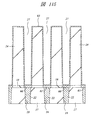
【0152】
その後、図113に示すように、前記実施の形態1と同様の方法で誘電体膜29の上部に上部電極30を形成することにより、下部電極28、誘電体膜29および上部電極30によって構成される情報蓄積用容量素子Cが完成する。
【0153】
図114は、下部電極28を構成するRu膜と各種下地材料との接着性を調べた結果を示すグラフである。使用した下地材料は、熱酸化で形成した酸化シリコン膜、プラズマCVD法で堆積した酸化シリコン膜(本発明で使用する酸化シリコン膜24に相当)、プラズマCVD法で堆積した窒化シリコン膜、スパッタリング法で堆積したTiN膜およびCVD法で堆積した酸化タンタル膜の5種類である。
【0154】
上記5種類の下地材料の上にスパッタリング法でRu膜を堆積し、その表面に荷重が加えられた針を当て、荷重を種々変化させて引っ掻き試験を行った。グラフは、この引っ掻き試験でRu膜が剥がれるときに針に加えた荷重によって剥離の程度を相対的に示したものであり、横軸は5種の下地材料、縦軸はRu膜が剥がれたときの荷重である。また、この引っ掻き試験では、成膜直後のRu膜と、700℃、1分の熱処理を行って緻密化したRu膜とを評価した。
【0155】
上記引っ掻き試験の結果、2種の酸化シリコン膜上のRu膜は、ほぼ50mNの荷重で剥離した。窒化シリコン膜上のRu膜は、緻密化処理を行うことによって接着性がやや向上したものの、成膜直後のものは、酸化シリコン膜上のRu膜と同じくほぼ50mNで剥離した。TiN膜上のRu膜は、100mNを少し越える程度の荷重で剥離した。これに対し、酸化タンタル膜上のRu膜は、200mNと極めて大きい荷重で剥離し、実用上十分な接着強度を有していることが判明した。
【0156】
このように、酸化シリコン膜24に開孔した溝27の内壁にRuからなる下部電極28を形成する際、溝27の内壁にあらかじめ酸化タンタル膜62を形成しておくことにより、Ru膜と下地との接着強度が顕著に向上する。これにより、Ru膜を緻密化する際の熱処理や誘電体膜(酸化タンタル膜)29を結晶化する際の熱処理によって下部電極28が剥離する不具合を確実に防止することができるので、情報蓄積用容量素子Cの下部電極28をRu膜で構成するDRAMの製造歩留まりを向上させることができる。
【0157】
Ruからなる下部電極28の下地材料には、酸化タンタルに比べると接着強度は低いがTiNを使用することもできる。この場合は、前記図108に示した工程に引き続き、図115に示すように、溝27の内壁および酸化シリコン膜24の表面にCVD法で膜厚10nm程度のTiN膜63を堆積する。TiN膜63は、四塩化チタン(TiCl4)とアンモニア(NH3)とを原料ガスに用いたCVD法で堆積する。
【0158】
Ruからなる下部電極28の下地材料としては、酸化タンタルやTiNの他、TaN(窒化タンタル)やTi02(酸化チタン)など、CVD法で成膜することのできる材料を使用することもできる。
【0159】
次に、図116に示すように、溝27の内部にフォトレジストなどの絶縁膜31を埋め込んだ後、溝27の外部のTiN膜63をドライエッチングによって除去する。TiN膜63は導電材料であるため、酸化タンタル膜62を使用した場合と異なり、溝27の底部(TiN層62の表面)に残すことができる。溝27の底部に残ったTiN膜63は、その下層のTiN層62と共に、下部電極28とプラグ22との界面で所望しないシリサイド反応が生じるのを防ぐバリア層として機能する。また、酸化シリコン膜24の表面のTiN膜63を除去する際は、溝27の側壁上端部のTiN膜63を下方に後退させる。これによって、後に堆積する誘電体膜(酸化タンタル膜)29との接触を避け、リーク電流の増加を防ぐことができる。
【0160】
次に、溝27の内部の絶縁膜31を除去した後、図117に示すように、溝27の内部に前述した方法で下部電極28を形成し、続いて図118に示すように、下部電極28の上部に酸化タンタル膜を堆積して誘電体膜29を形成した後、図119に示すように、誘電体膜29の上部に上部電極30を形成することにより、情報蓄積用容量素子Cが完成する。
【0161】
(実施の形態9)
本実施形態の製造方法は、スルーホール60の内部にTaN層61を形成するまでの工程が前記実施の形態8と同一であるため、その説明は省略し、以降の工程についてのみ説明する。
【0162】
まず、前記図107に示した工程に引き続き、図120に示すように、窒化シリコン膜18の上部にCVD法で酸化シリコン膜24を堆積し、必要に応じてその表面を化学機械研磨法で平坦化した後、酸化シリコン膜24の上部にCVD法で膜厚50nm程度の酸化タンタル膜64を堆積する。
【0163】
次に、図121に示すように、フォトレジスト膜(図示せず)をマスクにして酸化タンタル膜64と酸化シリコン膜24とをドライエッチングすることにより、その底部にスルーホール60内のTaN層61の表面が露出する溝27を形成する。
【0164】
次に、図122に示すように、溝27の内壁および酸化タンタル膜64の表面にCVD法で膜厚10nm程度の酸化タンタル膜62を堆積する。酸化タンタル膜は、前記実施の形態8と同様、例えば原料ガスにペンタエトキシタンタルと酸素とを用い、温度400℃〜450℃の条件で堆積する。
【0165】
次に、図123に示すように、異方性ドライエッチングによって溝27の底面の酸化タンタル膜62を除去し、溝27の側壁に酸化タンタル膜62を残す。このとき、酸化シリコン膜24の上部に堆積された2層の酸化タンタル膜64、62もドライエッチングされるが、溝27の底面の酸化タンタル膜62に比べて膜厚が厚いため、その一部はエッチングされずに残る。
【0166】
次に、図124に示すように、溝27の内壁にRuからなる下部電極28を形成する。下部電極28を形成するには、酸化タンタル膜64の上部および溝27の内部にスパッタリング法とCVD法とを用いて膜厚20nm程度の薄いRu膜を堆積する。次に、Ru膜の緻密化を図るために、真空中で700℃、1分程度の熱処理を行った後、溝27の内部にフォトレジストなどの絶縁膜を埋め込み、溝27の外部のRu膜をドライエッチングによって除去する。
【0167】
このように、本実施形態では、酸化シリコン膜24の表面に酸化タンタル膜64が堆積された状態で下部電極材料(Ru膜)を堆積するので、その直後にRu膜を緻密化するための熱処理を行っても、酸化シリコン膜24の表面のRu膜が下地から剥離して異物となる虞れがない。すなわち、Ru膜を緻密化してから溝27の内部にフォトレジストなどの絶縁膜を埋め込むことが可能となるため、溝27の内部に埋め込んだ絶縁膜中の汚染物質が下部電極材料(Ru膜)に転写される不具合を回避することができる。
【0168】
その後、図125に示すように、下部電極28の上部に酸化タンタル膜を堆積して誘電体膜29を形成し、さらに図126に示すように、誘電体膜29の上部に上部電極30を形成することにより、情報蓄積用容量素子Cが完成する。
【0169】
(実施の形態10)
前記実施の形態1〜9では、フォトレジスト膜をマスクにしたドライエッチングによって酸化シリコン膜24に溝27を形成したが、本実施形態では、酸化シリコンに対するエッチング選択比がフォトレジストよりも大きい材料をマスクにして溝27を形成する。
【0170】
まず、前記図107に示した工程に引き続き、図127に示すように、窒化シリコン膜18の上部にCVD法で酸化シリコン膜24を堆積し、必要に応じてその表面を化学機械研磨法で平坦化した後、酸化シリコン膜24の上部にWマスク65を形成する。Wマスク65を形成するには、酸化シリコン膜24の上部にCVD法で膜厚50nm程度のW膜を堆積し、続いてフォトレジスト膜をマスクにしたドライエッチングでW膜をパターニングする。
【0171】
次に、図128に示すように、Wマスク65を使用して酸化シリコン膜24をドライエッチングすることにより、その底部にスルーホール60内のTaN層61の表面が露出する溝27を形成する。Wは、酸化シリコンに対するエッチング選択比がフォトレジストよりも大きい。そのため、Wマスク65を使用して酸化シリコン膜24をドライエッチングした場合は、フォトレジスト膜を使用した場合に比べてマスクの目減りが小さくなるので、厚い膜厚の酸化シリコン膜24にアスペクト比の高い溝27を精度よく形成することができる。酸化シリコンに対するエッチング選択比がフォトレジストよりも大きいマスク材料として、Wの他、例えばMo(モリブデン)を使用することもできる。
【0172】
次に、図129に示すように、溝27の側壁に酸化タンタル膜62を形成する。酸化タンタル膜62を形成するには、溝27の内壁およびWマスク65の表面にCVD法で膜厚10nm程度の酸化タンタル膜62を堆積した後、異方性ドライエッチングによってWマスクの表面および溝27の底面の酸化タンタル膜62を除去する。溝27の側壁の酸化タンタル膜62は、下部電極材料であるRu膜と下地との接着強度を向上させるために形成する。
【0173】
次に、図130に示すように、溝27の内壁にRuからなる下部電極28を形成する。下部電極28を形成するには、Wマスク65の上部および溝27の内部にスパッタリング法とCVD法とを用いて膜厚20nm程度のRu膜を堆積し、続いてRu膜の緻密化を図るために、真空中で700℃、1分程度の熱処理を行った後、溝27の内部にフォトレジストなどの絶縁膜を埋め込み、溝27の外部のRu膜をドライエッチングによって除去する。
【0174】
このように、本実施形態では、酸化シリコン膜24の表面にRuとの接着性が高いWマスク65が形成された状態で下部電極材料(Ru膜)を堆積するので、その直後にRu膜を緻密化するための熱処理を行っても、酸化シリコン膜24の表面のRu膜が下地から剥離して異物となる虞れがない。すなわち、Ru膜を緻密化してから溝27の内部にフォトレジストなどの絶縁膜を埋め込むことが可能となるため、前記実施の形態9と同様、溝27の内部に埋め込んだ絶縁膜中の汚染物質が下部電極材料(Ru膜)に転写される不具合を回避することができる。
【0175】
その後、図131に示すように、下部電極28の上部に酸化タンタル膜を堆積して誘電体膜29を形成し、続いて誘電体膜29の上部に上部電極30を形成することにより、情報蓄積用容量素子Cが完成する。
【0176】
(実施の形態11)
本実施形態では、下部電極材料であるRu膜と酸化シリコン膜との接着力を向上させる他の方法について説明する。
【0177】
まず、前記図107に示した工程に引き続き、図132に示すように、窒化シリコン膜18の上部に酸化タンタル膜66を堆積し、続いてその上部に酸化シリコン膜24、酸化タンタル膜67、酸化シリコン膜24および酸化タンタル膜68を交互に堆積する。すなわち、本実施形態では、厚い膜厚の酸化シリコン膜24の下層、中間および上層に3層の酸化タンタル膜66、67、68を堆積する。酸化タンタル膜66、67、68はCVD法で堆積し、その膜厚は50nm〜100nm程度とする。なお、酸化シリコン膜24の中間にさらに1層〜複数層の酸化タンタル膜を堆積してもよい。
【0178】
次に、図133に示すように、フォトレジスト膜(図示せず)をマスクにして酸化タンタル膜66、67、68と酸化シリコン膜24とをドライエッチングすることにより、その底部にスルーホール60内のTaN層61の表面が露出する溝27を形成する。溝27は、前記実施の形態10と同様、Wマスク65を使用したドライエッチングで形成してもよい。このようにして形成された溝27の側壁には、酸化タンタル膜66、67、68が露出する。
【0179】
次に、図134に示すように、溝27の内壁にRuからなる下部電極28を形成する。下部電極28を形成するには、酸化タンタル膜68の上部および溝27の内部にスパッタリング法とCVD法とを用いて膜厚20nm程度のRu膜を堆積し、続いてRu膜の緻密化を図るために、真空中で700℃、1分程度の熱処理を行った後、溝27の内部にフォトレジストなどの絶縁膜を埋め込み、溝27の外部のRu膜をドライエッチングによって除去する。
【0180】
上記のような方法で溝27の内壁に下部電極28を形成した場合は、溝27の側壁で下部電極28と酸化タンタル膜66、67、68とが接触するため、下部電極28を構成するRu膜と下地との接着強度が向上する。
【0181】
その後、図135に示すように、下部電極28の上部に酸化タンタル膜を堆積して誘電体膜29を形成し、続いて誘電体膜29の上部に上部電極30を形成することにより、情報蓄積用容量素子Cが完成する。
【0182】
(実施の形態12)
前記実施の形態8〜11では、酸化シリコン膜24に溝27を形成する工程に先立って、スルーホール19内のプラグ22の表面にバリア層(TiN膜61)を形成する場合について説明したが、本実施形態では、酸化シリコン膜24に溝27を形成した後、プラグ22の表面にバリア層を形成する場合について説明する。
【0183】
まず、前記図36および図37に示した工程に引き続き、図136に示すように、酸化シリコン膜24および窒化シリコン膜18をドライエッチングすることにより、その底部にスルーホール19内のプラグ22の表面が露出する溝27を形成する。酸化シリコン膜24および窒化シリコン膜18のドライエッチングは、フォトレジスト膜をマスクにして行ってもよいが、前記実施の形態10と同様、酸化シリコンに対するエッチング選択比がフォトレジストよりも大きいWマスク65を使用することにより、深い溝27を精度よく形成することができる。
【0184】
次に、図137に示すように、溝27の側壁に酸化タンタル膜62を形成する。酸化タンタル膜62を形成するには、溝27の内壁およびWマスク65の表面にCVD法で膜厚10nm程度の酸化タンタル膜62を堆積した後、異方性ドライエッチングによってWマスクの表面および溝27の底面の酸化タンタル膜62を除去する。溝27の側壁の酸化タンタル膜62は、下部電極材料であるRu膜と下地との接着強度を向上させるために形成する。
【0185】
次に、図138に示すように、Wマスク65の上部および溝27の内部にCVD法で膜厚10nm程度のRu膜70aを堆積した後、図139に示すように、前記実施の形態1で説明した方法を用いてプラグ22の表面にRuシリサイド層25を形成し、続いてRuシリサイド層25の表面にRuシリコンナイトライド層26を形成する。
【0186】
次に、図140に示すように、Wマスク65の上部および溝27の内部にCVD法で膜厚10nm〜20nm程度のRu膜70bを堆積した後、図141に示すように、溝27の内壁にRu膜70aとRu膜70bとの積層膜からなる下部電極70を形成する。下部電極70を形成するには、溝27の内部にフォトレジストなどの絶縁膜を埋め込み、溝27の外部のRu膜70a、70bとWマスク65とをドライエッチングによって除去する。
【0187】
その後、図142に示すように、下部電極70の上部に酸化タンタル膜を堆積して誘電体膜29を形成し、続いて誘電体膜29の上部に上部電極30を形成することにより、下部電極70、誘電体膜29および上部電極30によって構成される情報蓄積用容量素子Cが完成する。
【0188】
以上、本発明者によってなされた発明を実施の形態に基づいて具体的に説明したが、本発明は前記実施の形態に限定されるものではなく、その要旨を逸脱しない範囲で種々変更可能であることはいうまでもない。
【0189】
本発明では、前記実施の形態1〜12で説明した構造、製造方法を種々組み合わせることができる。例えば図143に示すメモリセル構造は、前記実施の形態4と同様、プラグ13の表面に形成したRuシリサイド層35およびRuシリコンナイトライド層36と情報蓄積用容量素子Cの誘電体膜29とをスルーホール19内のプラグ37によって隔絶し、かつ前記実施の形態5〜7と同様、情報蓄積用容量素子Cの下部電極38を柱状体で構成したものである。また、図144に示すメモリセル構造は、図143に示すメモリセル構造において、さらに下部電極38の底部に酸素吸収層32を形成したものである。この酸素吸収層は、前記実施の形態7と同様、下部電極38の内部全体に形成してもよい。
【0190】
前記実施の形態1〜12では情報蓄積用容量素子の誘電体膜を酸化タンタルで構成したが、酸化チタン、あるいはチタン酸バリウム、チタン酸ストロンチウム、チタン酸バリウムストロンチウム、チタン酸鉛などのペロブスカイト型金属酸化物からなる高(強)誘電体またはそれらの積層体で構成することもできる。
【0191】
前記実施の形態1〜12では、DRAMおよびその製造プロセスに適用した場合について説明したが、汎用DRAMのみならず、ロジック混載DRAMやFeRAMなどにも適用することができる。
【0192】
【発明の効果】
本願によって開示される発明のうち、代表的なものによって得られる効果を簡単に説明すれば、以下のとおりである。
(1)本発明によれば、メモリセルの微細化がより一層進み、容量素子の下部電極とその下部の接続孔との合わせずれが不可避となった場合でも、下部電極のパターニング時に接続孔内のバリア層がエッチングされてシリコンプラグの表面が露出する不具合を防止すことができる。
(2)本発明によれば、容量素子の下部電極上に形成した誘電体膜を酸素雰囲気中で熱処理する際、下部電極を透過した酸素がバリア層自体を酸化して、高抵抗、低誘電率の酸化物層を形成する不具合を防止することができる。
(3)本発明によれば、容量素子の下部電極を構成する白金族金属膜と酸化シリコン膜との接着性を向上させることができる。
(4)本発明によれば、容量素子の表面積を増やすと共に誘電体膜の高誘電率化を図ることによって、メモリセルを微細化した場合においても所望する蓄積電荷量値を確保することができる。
(5)本発明によれば、厚い酸化シリコン膜に、情報蓄積用容量素子の下部電極を形成するための溝を形成した後、この溝の底部に露出したプラグの表面にシリコンの拡散のバリアとなる膜を形成することにより、例えばこの溝を形成する際に層間絶縁膜のオーバーエッチングによってプラグの側面が溝の底部に露出した場合でも、プラグの側面上に上記拡散バリア膜を形成することができる。これにより、下部電極を構成する金属膜と、例えば多結晶シリコン膜のようなシリコンを含む導電体膜によって構成されるプラグとの反応による形状異常の発生を防止したり、シリコンの拡散によって誘電体膜と下部電極との界面に酸化シリコンのような低誘電率の膜が形成される不具合を防止したりすることができる。
【図面の簡単な説明】
【図1】本発明の一実施の形態であるDRAMを形成したシリコンチップの全体平面図である。
【図2】本発明の一実施の形態であるDRAMを形成した半導体基板の要部断面図である。
【図3】本発明の一実施の形態であるDRAMを形成した半導体基板の要部断面図である。
【図4】本発明の一実施の形態であるDRAMの製造方法を示す半導体基板の要部平面図である。
【図5】本発明の一実施の形態であるDRAMの製造方法を示す半導体基板の要部断面図である。
【図6】本発明の一実施の形態であるDRAMの製造方法を示す半導体基板の要部断面図である。
【図7】本発明の一実施の形態であるDRAMの製造方法を示す半導体基板の要部断面図である。
【図8】本発明の一実施の形態であるDRAMの製造方法を示す半導体基板の要部平面図である。
【図9】本発明の一実施の形態であるDRAMの製造方法を示す半導体基板の要部断面図である。
【図10】本発明の一実施の形態であるDRAMの製造方法を示す半導体基板の要部断面図である。
【図11】本発明の一実施の形態であるDRAMの製造方法を示す半導体基板の要部断面図である。
【図12】本発明の一実施の形態であるDRAMの製造方法を示す半導体基板の要部断面図である。
【図13】本発明の一実施の形態であるDRAMの製造方法を示す半導体基板の要部断面図である。
【図14】本発明の一実施の形態であるDRAMの製造方法を示す半導体基板の要部平面図である。
【図15】本発明の一実施の形態であるDRAMの製造方法を示す半導体基板の要部断面図である。
【図16】本発明の一実施の形態であるDRAMの製造方法を示す半導体基板の要部断面図である。
【図17】本発明の一実施の形態であるDRAMの製造方法を示す半導体基板の要部断面図である。
【図18】本発明の一実施の形態であるDRAMの製造方法を示す半導体基板の要部断面図である。
【図19】本発明の一実施の形態であるDRAMの製造方法を示す半導体基板の要部断面図である。
【図20】本発明の一実施の形態であるDRAMの製造方法を示す半導体基板の要部断面図である。
【図21】本発明の一実施の形態であるDRAMの製造方法を示す半導体基板の要部断面図である。
【図22】本発明の一実施の形態であるDRAMの製造方法を示す半導体基板の要部断面図である。
【図23】本発明の一実施の形態であるDRAMの製造方法を示す半導体基板の要部断面図である。
【図24】本発明の一実施の形態であるDRAMの製造方法を示す半導体基板の要部断面図である。
【図25】本発明の一実施の形態であるDRAMの製造方法を示す半導体基板の要部平面図である。
【図26】本発明の一実施の形態であるDRAMの製造方法を示す半導体基板の要部断面図である。
【図27】本発明の一実施の形態であるDRAMの製造方法を示す半導体基板の要部断面図である。
【図28】本発明の一実施の形態であるDRAMの製造方法を示す半導体基板の要部断面図である。
【図29】本発明の一実施の形態であるDRAMの製造方法を示す半導体基板の要部平面図である。
【図30】本発明の一実施の形態であるDRAMの製造方法を示す半導体基板の要部断面図である。
【図31】本発明の一実施の形態であるDRAMの製造方法を示す半導体基板の要部断面図である。
【図32】本発明の一実施の形態であるDRAMの製造方法を示す半導体基板の要部断面図である。
【図33】本発明の一実施の形態であるDRAMの製造方法を示す半導体基板の要部断面図である。
【図34】本発明の一実施の形態であるDRAMの製造方法を示す半導体基板の要部断面図である。
【図35】本発明の一実施の形態であるDRAMの製造方法を示す半導体基板の要部断面図である。
【図36】本発明の一実施の形態であるDRAMの製造方法を示す半導体基板の要部断面図である。
【図37】本発明の一実施の形態であるDRAMの製造方法を示す半導体基板の要部断面図である。
【図38】本発明の一実施の形態であるDRAMの製造方法を示す半導体基板の要部平面図である。
【図39】本発明の一実施の形態であるDRAMの製造方法を示す半導体基板の要部断面図である。
【図40】本発明の一実施の形態であるDRAMの製造方法を示す半導体基板の要部断面図である。
【図41】本発明の一実施の形態であるDRAMの製造方法を示す半導体基板の要部断面図である。
【図42】本発明の一実施の形態であるDRAMの製造方法を示す半導体基板の要部断面図である。
【図43】本発明の一実施の形態であるDRAMの製造方法を示す半導体基板の要部断面図である。
【図44】本発明の一実施の形態であるDRAMの製造方法を示す半導体基板の要部断面図である。
【図45】本発明の一実施の形態であるDRAMの製造方法を示す半導体基板の要部断面図である。
【図46】本発明の一実施の形態であるDRAMの製造方法を示す半導体基板の要部断面図である。
【図47】本発明の一実施の形態であるDRAMの製造方法を示す半導体基板の要部断面図である。
【図48】本発明の一実施の形態であるDRAMの製造方法を示す半導体基板の要部断面図である。
【図49】本発明の一実施の形態であるDRAMの製造方法を示す半導体基板の要部断面図である。
【図50】本発明の一実施の形態であるDRAMの製造方法を示す半導体基板の要部断面図である。
【図51】本発明の一実施の形態であるDRAMの製造方法を示す半導体基板の要部断面図である。
【図52】本発明の一実施の形態であるDRAMの製造方法を示す半導体基板の要部断面図である。
【図53】本発明の一実施の形態であるDRAMの製造方法を示す半導体基板の要部断面図である。
【図54】本発明の一実施の形態であるDRAMの製造方法を示す半導体基板の要部断面図である。
【図55】本発明の一実施の形態であるDRAMの製造方法を示す半導体基板の要部断面図である。
【図56】本発明の一実施の形態であるDRAMの製造方法を示す半導体基板の要部断面図である。
【図57】本発明の一実施の形態であるDRAMの製造方法を示す半導体基板の要部断面図である。
【図58】本発明の一実施の形態であるDRAMの製造方法を示す半導体基板の要部断面図である。
【図59】本発明の他の実施の形態であるDRAMの製造方法を示す半導体基板の要部拡大断面図である。
【図60】本発明の他の実施の形態であるDRAMの製造方法を示す半導体基板の要部拡大断面図である。
【図61】本発明の他の実施の形態であるDRAMの製造方法を示す半導体基板の要部拡大断面図である。
【図62】本発明の他の実施の形態であるDRAMの製造方法を示す半導体基板の要部拡大断面図である。
【図63】本発明の他の実施の形態であるDRAMの製造方法を示す半導体基板の要部拡大断面図である。
【図64】本発明の他の実施の形態であるDRAMの製造方法を示す半導体基板の要部拡大断面図である。
【図65】本発明の他の実施の形態であるDRAMの製造方法を示す半導体基板の要部拡大断面図である。
【図66】本発明の他の実施の形態であるDRAMの製造方法を示す半導体基板の要部拡大断面図である。
【図67】本発明の他の実施の形態であるDRAMの製造方法を示す半導体基板の要部拡大断面図である。
【図68】本発明の他の実施の形態であるDRAMの製造方法を示す半導体基板の要部拡大断面図である。
【図69】本発明の他の実施の形態であるDRAMの製造方法を示す半導体基板の要部拡大断面図である。
【図70】本発明の他の実施の形態であるDRAMの製造方法を示す半導体基板の要部拡大断面図である。
【図71】本発明の他の実施の形態であるDRAMの製造方法を示す半導体基板の要部拡大断面図である。
【図72】本発明の他の実施の形態であるDRAMの製造方法を示す半導体基板の要部断面図である。
【図73】本発明の他の実施の形態であるDRAMの製造方法を示す半導体基板の要部断面図である。
【図74】本発明の他の実施の形態であるDRAMの製造方法を示す半導体基板の要部断面図である。
【図75】本発明の他の実施の形態であるDRAMの製造方法を示す半導体基板の要部断面図である。
【図76】本発明の他の実施の形態であるDRAMの製造方法を示す半導体基板の要部断面図である。
【図77】本発明の他の実施の形態であるDRAMの製造方法を示す半導体基板の要部断面図である。
【図78】本発明の他の実施の形態であるDRAMの製造方法を示す半導体基板の要部断面図である。
【図79】本発明の他の実施の形態であるDRAMの製造方法を示す半導体基板の要部断面図である。
【図80】本発明の他の実施の形態であるDRAMの製造方法を示す半導体基板の要部断面図である。
【図81】本発明の他の実施の形態であるDRAMの製造方法を示す半導体基板の要部断面図である。
【図82】本発明の他の実施の形態であるDRAMの製造方法を示す半導体基板の要部断面図である。
【図83】本発明の他の実施の形態であるDRAMの製造方法を示す半導体基板の要部断面図である。
【図84】本発明の他の実施の形態であるDRAMの製造方法を示す半導体基板の要部断面図である。
【図85】本発明の他の実施の形態であるDRAMの製造方法を示す半導体基板の要部断面図である。
【図86】本発明の他の実施の形態であるDRAMの製造方法を示す半導体基板の要部断面図である。
【図87】本発明の他の実施の形態であるDRAMの製造方法を示す半導体基板の要部断面図である。
【図88】本発明の他の実施の形態であるDRAMの製造方法を示す半導体基板の要部断面図である。
【図89】本発明の他の実施の形態であるDRAMの製造方法を示す半導体基板の要部断面図である。
【図90】本発明の他の実施の形態であるDRAMの製造方法を示す半導体基板の要部断面図である。
【図91】本発明の他の実施の形態であるDRAMの製造方法を示す半導体基板の要部断面図である。
【図92】本発明の他の実施の形態であるDRAMの製造方法を示す半導体基板の要部断面図である。
【図93】本発明の他の実施の形態であるDRAMの製造方法を示す半導体基板の要部拡大断面図である。
【図94】本発明の他の実施の形態であるDRAMの製造方法を示す半導体基板の要部拡大断面図である。
【図95】本発明の他の実施の形態であるDRAMの製造方法を示す半導体基板の要部拡大断面図である。
【図96】本発明の他の実施の形態であるDRAMの製造方法を示す半導体基板の要部拡大断面図である。
【図97】本発明の他の実施の形態であるDRAMの製造方法を示す半導体基板の要部拡大断面図である。
【図98】本発明の他の実施の形態であるDRAMの製造方法を示す半導体基板の要部拡大断面図である。
【図99】本発明の他の実施の形態であるDRAMの製造方法を示す半導体基板の要部拡大断面図である。
【図100】本発明の他の実施の形態であるDRAMの製造方法を示す半導体基板の要部拡大断面図である。
【図101】本発明の他の実施の形態であるDRAMの製造方法を示す半導体基板の要部拡大断面図である。
【図102】本発明の他の実施の形態であるDRAMの製造方法を示す半導体基板の要部拡大断面図である。
【図103】本発明の他の実施の形態であるDRAMの製造方法を示す半導体基板の要部拡大断面図である。
【図104】本発明の他の実施の形態であるDRAMの製造方法を示す半導体基板の要部拡大断面図である。
【図105】本発明の他の実施の形態であるDRAMの製造方法を示す半導体基板の要部拡大断面図である。
【図106】本発明の他の実施の形態であるDRAMの製造方法を示す半導体基板の要部断面図である。
【図107】本発明の他の実施の形態であるDRAMの製造方法を示す半導体基板の要部断面図である。
【図108】本発明の他の実施の形態であるDRAMの製造方法を示す半導体基板の要部断面図である。
【図109】本発明の他の実施の形態であるDRAMの製造方法を示す半導体基板の要部断面図である。
【図110】本発明の他の実施の形態であるDRAMの製造方法を示す半導体基板の要部断面図である。
【図111】本発明の他の実施の形態であるDRAMの製造方法を示す半導体基板の要部断面図である。
【図112】本発明の他の実施の形態であるDRAMの製造方法を示す半導体基板の要部断面図である。
【図113】本発明の他の実施の形態であるDRAMの製造方法を示す半導体基板の要部断面図である。
【図114】下部電極を構成するRu膜と各種下地材料との接着性を示すグラフである。
【図115】本発明の他の実施の形態であるDRAMの製造方法を示す半導体基板の要部拡大断面図である。
【図116】本発明の他の実施の形態であるDRAMの製造方法を示す半導体基板の要部拡大断面図である。
【図117】本発明の他の実施の形態であるDRAMの製造方法を示す半導体基板の要部拡大断面図である。
【図118】本発明の他の実施の形態であるDRAMの製造方法を示す半導体基板の要部拡大断面図である。
【図119】本発明の他の実施の形態であるDRAMの製造方法を示す半導体基板の要部拡大断面図である。
【図120】本発明の他の実施の形態であるDRAMの製造方法を示す半導体基板の要部拡大断面図である。
【図121】本発明の他の実施の形態であるDRAMの製造方法を示す半導体基板の要部拡大断面図である。
【図122】本発明の他の実施の形態であるDRAMの製造方法を示す半導体基板の要部拡大断面図である。
【図123】本発明の他の実施の形態であるDRAMの製造方法を示す半導体基板の要部拡大断面図である。
【図124】本発明の他の実施の形態であるDRAMの製造方法を示す半導体基板の要部拡大断面図である。
【図125】本発明の他の実施の形態であるDRAMの製造方法を示す半導体基板の要部拡大断面図である。
【図126】本発明の他の実施の形態であるDRAMの製造方法を示す半導体基板の要部拡大断面図である。
【図127】本発明の他の実施の形態であるDRAMの製造方法を示す半導体基板の要部拡大断面図である。
【図128】本発明の他の実施の形態であるDRAMの製造方法を示す半導体基板の要部拡大断面図である。
【図129】本発明の他の実施の形態であるDRAMの製造方法を示す半導体基板の要部拡大断面図である。
【図130】本発明の他の実施の形態であるDRAMの製造方法を示す半導体基板の要部拡大断面図である。
【図131】本発明の他の実施の形態であるDRAMの製造方法を示す半導体基板の要部拡大断面図である。
【図132】本発明の他の実施の形態であるDRAMの製造方法を示す半導体基板の要部拡大断面図である。
【図133】本発明の他の実施の形態であるDRAMの製造方法を示す半導体基板の要部拡大断面図である。
【図134】本発明の他の実施の形態であるDRAMの製造方法を示す半導体基板の要部拡大断面図である。
【図135】本発明の他の実施の形態であるDRAMの製造方法を示す半導体基板の要部拡大断面図である。
【図136】本発明の他の実施の形態であるDRAMの製造方法を示す半導体基板の要部拡大断面図である。
【図137】本発明の他の実施の形態であるDRAMの製造方法を示す半導体基板の要部拡大断面図である。
【図138】本発明の他の実施の形態であるDRAMの製造方法を示す半導体基板の要部拡大断面図である。
【図139】本発明の他の実施の形態であるDRAMの製造方法を示す半導体基板の要部拡大断面図である。
【図140】本発明の他の実施の形態であるDRAMの製造方法を示す半導体基板の要部拡大断面図である。
【図141】本発明の他の実施の形態であるDRAMの製造方法を示す半導体基板の要部拡大断面図である。
【図142】本発明の他の実施の形態であるDRAMの製造方法を示す半導体基板の要部拡大断面図である。
【図143】本発明の他の実施の形態であるDRAMの製造方法を示す半導体基板の要部断面図である。
【図144】本発明の他の実施の形態であるDRAMの製造方法を示す半導体基板の要部断面図である。
【符号の説明】
1 シリコン基板
1A シリコンチップ
2 素子分離溝
3 p型ウエル
4 酸化シリコン膜
5 ゲート絶縁膜
6 ゲート電極
7 酸化シリコン膜
8 n型半導体領域(ソース、ドレイン)
9 窒化シリコン膜
10 酸化シリコン膜
11、12 コンタクトホール
13 プラグ
14 酸化シリコン膜
15 スルーホール
16 プラグ
17 酸化シリコン膜
18 窒化シリコン膜
19 スルーホール
20 多結晶シリコン膜
21 サイドウォールスペーサ
22 プラグ
23 Ru膜
24 酸化シリコン膜
25 Ruシリサイド層
26 Ruシリコンナイトライド層
27 溝
28 下部電極
28a〜28d Ru膜
29 誘電体膜
30 上部電極
31 絶縁膜
32 酸素吸収層
32a、32b Wシリサイド膜
33 絶縁膜
34 Ru膜
35 Ruシリサイド層
36 Ruシリコンナイトライド層
37a Ru膜
37 プラグ
38a〜38f Ru膜
38 下部電極
39 誘電体膜
40 上部電極
50 多結晶シリコン膜
51 酸素吸収層
60 スルーホール
61 TaN層
62 酸化タンタル膜
63 TiN膜
64 酸化タンタル膜
65 Wマスク
66、67、68 酸化タンタル膜
70a、70b Ru膜
70 下部電極
BL ビット線
C 情報蓄積容量素子(キャパシタ)
L 活性領域
MARY メモリアレイ
Qs メモリセル選択用MISFET
SA センスアンプ
WD ワードドライバ
WL ワード線[0001]
BACKGROUND OF THE INVENTION
The present invention relates to a semiconductor integrated circuit device and a manufacturing technique thereof, and more particularly to a technology effective when applied to a semiconductor integrated circuit device having a DRAM (Dynamic Random Access Memory).
[0002]
[Prior art]
DRAM memory cells are generally arranged at the intersections of a plurality of word lines and a plurality of bit lines arranged in a matrix on the main surface of a semiconductor substrate. One memory cell is composed of one MISFET (Metal Insulator Semiconductor Field Effect Transistor) for selecting it and one information storage capacitor (capacitor) connected in series to the MISFET.
[0003]
The memory cell selection MISFET is formed in an active region surrounded by an element isolation region, and is mainly composed of a gate insulating film, a gate electrode integrated with a word line, and a pair of semiconductor regions constituting a source and a drain. Is done. Two memory cell selection MISFETs are normally formed in one active region, and one of the source and drain (semiconductor region) of these two MISFETs is shared at the center of the active region.
[0004]
A bit line is arranged above the memory cell selection MISFET and is connected to one of a source and a drain (semiconductor region) through a connection hole in which a plug made of polycrystalline silicon or the like is embedded (a semiconductor region shared by two MISFETs). ) And electrically connected. The information storage capacitive element is disposed above the bit line and electrically connected to the other of the source and drain (semiconductor region) of the memory cell selection MISFET through a connection hole in which a plug made of polycrystalline silicon or the like is embedded. Connected to.
[0005]
As described above, recent DRAMs employ a three-dimensional structure in which an information storage capacitive element is arranged above a bit line as a countermeasure to compensate for a decrease in the amount of stored charge accompanying memory cell miniaturization. However, in the case of a large-capacity DRAM of 256 megabits or more where the miniaturization of memory cells is further advanced, it is considered that it is difficult to compensate for the decrease in the amount of stored charge only by three-dimensionalizing the information storage capacitor element.
[0006]
Therefore, as a dielectric film of the information storage capacitor element, tantalum oxide (Ta 2 O Five ), Strontium titanate (STO), barium strontium titanate (BST) and other high dielectric (ferroelectric) materials are being studied. That is, tantalum oxide has a high relative dielectric constant of about 40 and STO and BST are about 200 to 500. Therefore, by using these high (strong) dielectric materials as dielectric films, silicon nitride (relative dielectric constant) This is because a significant increase in the amount of stored charge can be expected as compared to the case of using = 7 to 8) for the dielectric film.
[0007]
However, these high (strong) dielectric materials cannot be obtained with a high relative dielectric constant simply by film formation, and the leakage current of the film is large, so that heat treatment is performed in an oxygen atmosphere at 750 ° C. or higher after film formation. By doing so, it is necessary to improve the crystallization and the film quality. Therefore, when a high (strong) dielectric material is used for the dielectric film of the information storage capacitive element, there arises a problem of MISFET characteristic fluctuation due to this high temperature heat treatment.
[0008]
Therefore, when a high (strong) dielectric material is used for the dielectric film, a platinum group metal such as Ru (ruthenium), Pt (platinum), or Ir (iridium) is used for the underlying lower electrode. When a high (strong) dielectric film is deposited on these metal surfaces, the film can be crystallized and the film quality can be improved by a heat treatment at a temperature lower than 100 ° C. over a normal heat treatment such as 650 ° C. to 600 ° C. Therefore, the amount of heat treatment in the entire manufacturing process can be reduced, and the characteristic variation of the MISFET can be prevented.
[0009]
On the other hand, when the platinum group metal as described above is used as the lower electrode material, since these are materials that easily transmit oxygen, oxygen is formed after forming a high (strong) dielectric film on the surface of the lower electrode. When heat treatment is performed in an atmosphere, oxygen passes through the high (strong) dielectric film and the lower electrode and reaches the lower silicon plug, and the platinum group metal and silicon react to cause unwanted metal at the interface between the two. There is a problem that a silicide layer is formed. As a countermeasure, it has been proposed to form a barrier layer that prevents the reaction between the lower electrode made of a platinum group metal and the silicon plug.
[0010]
Japanese Patent Application Laid-Open No. 10-79481 discloses that a platinum group metal and silicon are mutually diffused by a heat treatment at 700 to 800 ° C. when a silicon oxide film is reflowed and planarized, and a metal silicide layer is formed. Ti (titanium), W (tungsten), Ta (tantalum), Co (cobalt), and Mo (cobalt) are used as barrier layers to prevent the silicide layer from being oxidized to form a silicon oxide layer having a low dielectric constant. A conductive layer (metal silicon nitride layer) containing a refractory metal such as molybdenum) and silicon and nitrogen is proposed. The barrier layer is preferably formed by laminating a first layer containing columnar crystals or amorphous and a second layer containing granular crystals. Further, it is preferable that a layer containing Ti that improves the adhesion between the barrier layer and the silicon plug is formed.
[0011]
Japanese Patent Laid-Open No. 10-209394 discloses that when a lower electrode is formed in the upper part of a connection hole in which a silicon plug is embedded, if a mask misalignment of both occurs, the dielectric film formed on the upper part of the lower electrode and the lower part of the lower electrode As a result of this contact with the silicon plug, oxygen and silicon in the dielectric film react to form a high-resistance silicon oxide film, or oxygen in the dielectric film becomes insufficient and leakage current increases. Pointed out. As a countermeasure, this publication discloses a technique of providing a blocking film made of silicon nitride between a dielectric film and a silicon plug.
[0012]
Japanese Patent Application Laid-Open No. 11-307736 relates to a ferroelectric memory, and iridium oxide (IrO x ), A dielectric film made of a ferroelectric material such as PZT (lead zirconate titanate), and an upper electrode made of a white metal such as Pt. Discloses a technique of forming a tantalum silicon nitride (TaSiN) film as a diffusion barrier layer and forming an Ir film as an oxygen blocking film on the diffusion barrier layer.
[0013]
[Problems to be solved by the invention]
As described above, in the prior art, when a lower electrode made of a platinum group metal is formed on an upper part of a connection hole in which a silicon plug is embedded, a high (strong) dielectric film is formed on the lower electrode and heat treatment is performed. An undesired reaction between the platinum group metal and the silicon plug is prevented by forming a barrier layer on the silicon plug in advance.
[0014]
However, as memory cells are further miniaturized, misalignment between the lower electrode and the lower connection hole becomes unavoidable, and the barrier layer in the connection hole is etched during patterning of the lower electrode to expose the surface of the silicon plug. There are things to do. In this case, since a part of the high (strong) dielectric film formed on the lower electrode is in direct contact with the silicon plug, there arises a problem that the dielectric breakdown voltage of the dielectric film is lowered and the leakage current is increased.
[0015]
Further, as a result of investigations by the present inventors, even when a barrier layer is formed on a silicon plug, if heat treatment of a high (strong) dielectric film is performed in a high-temperature oxygen atmosphere, oxygen transmitted through the lower electrode However, it has been found that the barrier layer itself is oxidized to form an oxide layer having a high resistance and a low dielectric constant.
[0016]
In addition, the inventors deposited a thick silicon oxide film on the upper part of the connection hole in which the silicon plug is embedded, and then etched the silicon oxide film to form a deep groove reaching the surface of the silicon plug. We are investigating the process of forming a lower electrode by depositing a platinum group metal film on the inner wall of the metal. However, because the adhesion between the platinum group metal film and the silicon oxide film is low, the lower electrode is formed during the manufacturing process. It has been found that peeling may occur between the electrode and the silicon oxide film.
[0017]
The object of the present invention is to provide a barrier layer in a connection hole at the time of patterning of the lower electrode even when the miniaturization of the memory cell is further advanced and the misalignment between the lower electrode of the capacitive element and the connection hole in the lower part is unavoidable. It is an object of the present invention to provide a technique for preventing a problem that the surface of a silicon plug is exposed by etching.
[0018]
Another object of the present invention is that when the dielectric film formed on the lower electrode of the capacitor element is heat-treated in an oxygen atmosphere, the oxygen transmitted through the lower electrode oxidizes the barrier layer itself, resulting in a high resistance, low dielectric constant. An object of the present invention is to provide a technique for preventing a problem of forming the oxide layer.
[0019]
Another object of the present invention is to provide a technique for improving the adhesion between a platinum group metal film and a silicon oxide film constituting a lower electrode of a capacitive element.
[0020]
Another object of the present invention is to secure a desired accumulated charge amount value even when the memory cell is miniaturized by increasing the surface area of the capacitor element and increasing the dielectric constant of the dielectric film. It is to provide technology that can be used.
[0021]
The above and other objects and novel features of the present invention will be apparent from the description of this specification and the accompanying drawings.
[0022]
[Means for Solving the Problems]
Of the inventions disclosed in the present application, the outline of typical ones will be briefly described as follows.
[0023]
In the semiconductor integrated circuit device of the present invention, a capacitive element including a first electrode made of a first metal, a dielectric film, and a second electrode made of a second metal is formed on a main surface of a semiconductor substrate. The first semiconductor region of the semiconductor substrate and the first electrode of the capacitor element are electrically connected via a silicon plug inside a first connection hole formed in the first insulating film above the first semiconductor region. A metal silicide layer is formed on the surface of the silicon plug, and at least one of a metal silicon nitride layer and a metal silicon oxynitride layer is formed on the surface of the metal silicide layer. .
[0024]
In the semiconductor integrated circuit device of the present invention, a capacitive element including a first electrode made of a first metal, a dielectric film, and a second electrode made of a second metal is formed on a main surface of a semiconductor substrate. A first semiconductor region formed in the semiconductor substrate and a first electrode of the capacitive element, a silicon plug inside a second connection hole formed in a second insulating film above the first semiconductor region; Electrically connected via a metal plug inside the first connection hole formed in the first insulating film above the second insulating film, and a metal silicide layer is formed on the surface of the silicon plug; At least one of a metal silicon nitride layer and a metal silicon oxynitride layer is formed on the surface of the metal silicide layer.
[0025]
The method for manufacturing a semiconductor integrated circuit device of the present invention includes the following steps:
(A) forming a first connection hole in the first insulating film above the first semiconductor region after forming a first insulating film on the main surface of the semiconductor substrate on which the first semiconductor region is formed;
(B) forming a silicon plug inside the first connection hole;
(C) After the third insulating film is formed on the first insulating film, the third insulating film on the first connection hole is etched to expose the surface of the silicon plug at the bottom. Forming a groove;
(D) forming a metal silicon nitride layer on the surface of the metal silicide layer after forming a metal silicide layer on the surface of the silicon plug;
(E) forming a first electrode of a capacitive element made of a first metal in the groove and electrically connecting the first electrode and the first semiconductor region through the first connection hole;
(F) a step of heat-treating the dielectric film in an atmosphere containing oxygen after forming the dielectric film of the capacitive element on the first electrode;
(G) forming a second electrode of the capacitive element made of a second metal on the dielectric film;
[0026]
The method for manufacturing a semiconductor integrated circuit device of the present invention includes the following steps:
(A) forming a second connection hole in the second insulating film above the first semiconductor region after forming a second insulating film on the main surface of the semiconductor substrate on which the first semiconductor region is formed;
(B) forming a silicon plug inside the second connection hole;
(C) After the first insulating film is formed on the second insulating film, the surface of the silicon plug is exposed at the bottom by etching the first insulating film above the second connection hole. Forming a first connection hole;
(D) forming a metal silicon nitride layer on the surface of the metal silicide layer after forming a metal silicide layer on the surface of the silicon plug;
(E) forming a metal plug inside the first connection hole;
(F) After the third insulating film is formed on the first insulating film, the surface of the metal plug is exposed at the bottom by etching the third insulating film above the first connection hole. Forming a groove;
(G) forming a first electrode of a capacitor element made of a first metal inside the groove, and electrically connecting the first electrode and the first semiconductor region through the first connection hole and the second connection hole; Connecting,
(H) a step of heat-treating the dielectric film in an atmosphere containing oxygen after forming the dielectric film of the capacitive element on the first electrode;
(I) forming a second electrode of the capacitive element made of a second metal on the dielectric film;
[0027]
The method for manufacturing a semiconductor integrated circuit device of the present invention includes the following steps:
(A) forming a first connection hole in the first insulating film above the first semiconductor region after forming a first insulating film on the main surface of the semiconductor substrate on which the first semiconductor region is formed;
(B) forming a silicon plug inside the first connection hole;
(C) After the third insulating film is formed on the first insulating film, the third insulating film on the first connection hole is etched to expose the surface of the silicon plug at the bottom. Forming a groove;
(D) forming a metal silicon nitride layer on the surface of the metal silicide layer after forming a metal silicide layer on the surface of the silicon plug;
(E) forming the first metal film on the third insulating film including the inside of the trench to embed the first metal film in the trench and then the first metal outside the trench; Removing the film;
(F) By removing the third insulating film by etching, a first electrode of a capacitor element made of a columnar first metal film is formed on the first connection hole, and the first electrode is formed through the first connection hole. Electrically connecting the first electrode and the first semiconductor region;
(G) a step of heat-treating the dielectric film in an oxygen-containing atmosphere after forming the dielectric film of the capacitive element on the first electrode;
(H) forming a second electrode of the capacitive element made of a second metal on the dielectric film;
[0028]
The method for manufacturing a semiconductor integrated circuit device of the present invention includes the following steps:
(A) forming a second connection hole in the second insulating film above the first semiconductor region after forming a second insulating film on the main surface of the semiconductor substrate on which the first semiconductor region is formed;
(B) forming a silicon plug inside the second connection hole;
(C) After the first insulating film is formed on the second insulating film, the surface of the silicon plug is exposed at the bottom by etching the first insulating film above the second connection hole. Forming a first connection hole;
(D) forming a metal silicon nitride layer on the surface of the metal silicide layer after forming a metal silicide layer on the surface of the silicon plug;
(E) forming a metal plug inside the first connection hole;
(F) After the third insulating film is formed on the first insulating film, the surface of the metal plug is exposed at the bottom by etching the third insulating film above the first connection hole. Forming a groove;
(G) forming the first metal film on the third insulating film including the inside of the groove to embed the first metal film in the groove and then the first metal outside the groove; Removing the film;
(H) By removing the third insulating film by etching, a first electrode of a capacitor element made of the columnar first metal film is formed on the first connection hole, and the first connection hole and the first connection hole Electrically connecting the first electrode and the first semiconductor region through a second connection hole;
(I) a step of heat-treating the dielectric film in an atmosphere containing oxygen after forming the dielectric film of the capacitive element on the first electrode;
(J) forming a second electrode of the capacitive element made of a second metal on the dielectric film;
[0029]
DETAILED DESCRIPTION OF THE INVENTION
Hereinafter, embodiments of the present invention will be described in detail with reference to the drawings. Note that components having the same function are denoted by the same reference symbols throughout the drawings for describing the embodiments, and the repetitive description thereof will be omitted.
[0030]
(Embodiment 1)
FIG. 1 is an overall plan view of a silicon chip 1A on which a DRAM of this embodiment is formed. A DRAM having a storage capacity of, for example, 256 Mbit (megabit) to 1 Gbit (gigabit) is formed on the main surface of the rectangular silicon chip 1A. This DRAM is composed of a storage section divided into a plurality of memory arrays (MARY) and a peripheral circuit section arranged around them. At the center of the main surface of the silicon chip 1A, a control circuit such as a word driver WD and a data line selection circuit, an input / output circuit, a bonding pad, and the like are arranged. A sense amplifier SA is disposed between the memory arrays (MARY).
[0031]
The memory array (MARY) is composed of a plurality of word lines and bit lines arranged in a matrix and a plurality of memory cells arranged at intersections thereof. 2 and 3 are sectional views of a silicon substrate (hereinafter simply referred to as a substrate) 1 showing a part of a DRAM memory array (MARY).
[0032]
One memory cell for storing 1-bit information includes one memory cell selection MISFET Qs formed in the p-type well 2 of the
[0033]
As shown in the figure, the memory cell employs a stacked capacitor structure in which an information storage capacitor element C, which is an information storage capacitor section, is disposed above the memory cell selection MISFET Qs. The information storage capacitive element C includes a lower electrode (storage node) 28 made of a metal containing Ru (ruthenium) as a main component, and Ta formed on the
[0034]
The
[0035]
At the interface between the
[0036]
Next, a method for manufacturing the DRAM of this embodiment will be described in the order of steps with reference to FIGS. Of the DRAM manufacturing processes described below, the processes from forming the memory cell selecting MISFET Qs on the main surface of the
[0037]
First, FIG. 4 (plan view of the main part of the memory array), FIG. 5 (cross-sectional view taken along line AA in FIG. 4), FIG. 6 (cross-sectional view taken along line BB in FIG. 4), and FIG. As shown in (a cross-sectional view taken along the line CC in FIG. 4), an
[0038]
As shown in FIG. 4, by forming the
[0039]
Next, B (boron) is ion-implanted into the
[0040]
Next, as shown in FIGS. 8 to 10, the
[0041]
Next, as shown in FIGS. 11 to 13, As (arsenic) or P (phosphorus) ions are implanted into the p-
[0042]
Next, as shown in FIGS. 14 to 17, a silicon nitride film 9 (film thickness of 50 nm) and a silicon oxide film 10 (film thickness of about 600 nm) are deposited on the
[0043]
Next, as shown in FIGS. 18 and 19, plugs 13 are formed in the contact holes 11 and 12. In order to form the
[0044]
Next, after depositing a silicon oxide film 14 (film thickness of about 150 nm) on the
[0045]
Next, as shown in FIGS. 23 and 24, a
[0046]
Next, as shown in FIGS. 25 to 28, the bit line BL is formed on the
[0047]
Next, as shown in FIGS. 29 to 32, a
[0048]
The through
[0049]
As shown in FIGS. 29 and 32, the center of the through
[0050]
Next, after the mask (
[0051]
Next, as shown in FIGS. 36 and 37, a
[0052]
Next, as shown in FIGS. 38 to 40, the
[0053]
The
[0054]
Next, as shown in FIGS. 41 and 42, a
[0055]
Next, as shown in FIGS. 43 and 44, a heat treatment is performed at 700 ° C. for about 1 minute in a non-oxidizing gas atmosphere such as nitrogen, and the
[0056]
The
[0057]
Next, as shown in FIGS. 45 and 46, a Ru
[0058]
The film thickness of the Ru
[0059]
It is also conceivable that the Ru
[0060]
The Ru
[0061]
As described above, in the present embodiment, the
[0062]
Next, as shown in FIGS. 47 and 48, a
[0063]
Next, as shown in FIGS. 51 and 52, the insulating
[0064]
Next, as shown in FIGS. 53 and 54, the insulating
[0065]
Next, as shown in FIGS. 55 and 56, a
[0066]
Although not particularly limited, in this embodiment, in order to effectively perform crystallization of the portion of the tantalum oxide film in contact with the
[0067]
In the case where the tantalum oxide film is formed twice and the heat treatment is performed twice, the heat treatment conditions after the first film formation are important, and the crystallization of the tantalum oxide film needs to be completed by the first heat treatment. If the tantalum oxide film is crystallized by this heat treatment, the tantalum oxide film formed in the second film formation is already crystallized upon completion of the film formation (homoepitaxial growth), so the second heat treatment is necessarily required. is not. This homoepitaxial growth is not limited to tantalum oxide, but is a common phenomenon although there are differences in the degree of metal oxides formed by the CVD method. However, in order to obtain a tantalum oxide film with less leakage current, it is better to perform the second heat treatment.
[0068]
By performing the heat treatment, the Ru
[0069]
In this embodiment, the heat treatment for crystallization of the tantalum oxide film constituting the
[0070]
Next, as shown in FIGS. 57 and 58, the
[0071]
The inside of the
[0072]
Through the steps so far, the information storage capacitive element C constituted by the
[0073]
Thereafter, about two layers of Al wiring are formed on the upper part of the information storage capacitor C with an interlayer insulating film interposed therebetween, and a passivation film is formed on the uppermost Al wiring, but these are not shown.
[0074]
As described above in detail, according to the present embodiment, the
[0075]
In the present embodiment, the
[0076]
Further, in the manufacturing method of the present embodiment, the
[0077]
The silicide layer formed on the surface of the
[0078]
Further, the lower electrode material is not limited to Ru, and may be composed of, for example, Pt, Ir (iridium) or the like. Ru used in the present embodiment may be ruthenium oxide by oxidizing itself when heat-treated in an excessive oxidizing atmosphere, which may cause inconvenience in a later process. There is an advantage of not forming things.
[0079]
Further, the upper electrode material of the information storage capacitor C is not limited to TiN, and may be composed of, for example, a metal such as W, Ru, Pt, or Ir, or a laminate of these metals and TiN. it can.
[0080]
(Embodiment 2)
In the manufacturing method of the present embodiment, the steps until the
[0081]
First, following the process shown in FIG. 46, as shown in FIG. 59, a
[0082]
Next, as shown in FIG. 60, a
[0083]
Next, as shown in FIG. 61, a
[0084]
Next, as shown in FIG. 62, the
[0085]
Next, as shown in FIG. 63, a
[0086]
Next, as shown in FIG. 64, by combining the CVD method and the sputtering method, a TiN film is deposited on top of the
[0087]
As described above, in this embodiment, the
[0088]
The
[0089]
The conductive material constituting the
[0090]
For example, pure metals such as W and Ti are ideal as a conductive material that absorbs oxygen. However, since the volume changes due to oxidation, when used as the
[0091]
The most preferable conductive material constituting the
[0092]
(Embodiment 3)
In the second embodiment, the
[0093]
First, following the step shown in FIG. 46, as shown in FIG. 65, a
[0094]
Next, as shown in FIG. 66, a
[0095]
Next, as shown in FIG. 67, an insulating
[0096]
Next, after removing the insulating
[0097]
Next, as shown in FIG. 70, a
[0098]
Next, as shown in FIG. 71, the
[0099]
In this embodiment, since the
[0100]
The
[0101]
The conductive material constituting the
[0102]
When the
[0103]
As described above, when the
[0104]
(Embodiment 4)
In the first to third embodiments, the
[0105]
First, as shown in FIG. 72, the through-
[0106]
Next, as shown in FIG. 73, a
[0107]
Next, as shown in FIG. 74, heat treatment is performed at 600 ° C. for about 1 minute in a non-oxidizing gas atmosphere such as nitrogen to embed the
[0108]
Next, as shown in FIG. 75, a Ru
[0109]
Next, as shown in FIG. 76, a
[0110]
Next, as shown in FIG. 78, a
[0111]
Next, as shown in FIG. 79, after forming the
[0112]
Next, as shown in FIG. 81, the
[0113]
Thus, in the present embodiment, the
[0114]
According to the present embodiment, the
[0115]
In this embodiment, the
[0116]
Further, as in the second and third embodiments, the
[0117]
Further, the
[0118]
(Embodiment 5)
In the DRAMs of the first to fourth embodiments, the
[0119]
In the manufacturing method of the present embodiment, the steps until the
[0120]
First, following the step shown in FIG. 46, as shown in FIGS. 83 and 84, a
[0121]
Next, as shown in FIGS. 85 and 86, the
[0122]
Next, as shown in FIGS. 89 and 90, a
[0123]
Next, as shown in FIGS. 91 and 92, a TiN film or the like is deposited on top of the
[0124]
Thus, according to the present embodiment, even when the
[0125]
Further, in the manufacturing method of the present embodiment, the
[0126]
Further, according to the present embodiment in which the
[0127]
(Embodiment 6)
In the DRAM of the present embodiment, the lower electrode of the information storage capacitor element C is formed of a columnar body as in the fifth embodiment, and an oxygen absorption layer is formed at the bottom of the lower electrode as in the second embodiment.
[0128]
First, following the process shown in FIG. 46, as shown in FIG. 93, a
[0129]
Next, as shown in FIG. 94, a
[0130]
Next, as shown in FIG. 95, a
[0131]
Next, as shown in FIG. 96, the
[0132]
Next, as shown in FIG. 98, a
[0133]
As described above, in this embodiment, the
[0134]
(Embodiment 7)
In the DRAM of this embodiment, the lower electrode of the information storage capacitive element C is formed of a columnar body as in the fifth and sixth embodiments, and an oxygen absorption layer is formed inside the lower electrode.
[0135]
First, following the process shown in FIG. 46, as shown in FIG. 99, a
[0136]
Next, as shown in FIG. 100, a
[0137]
Next, as shown in FIG. 101, heat treatment is performed in a non-oxidizing gas atmosphere such as nitrogen, and the
[0138]
In the case where the
[0139]
Next, as shown in FIG. 102, a
[0140]
Next, as shown in FIG. 103, the
[0141]
Next, as shown in FIG. 105, a
[0142]
In this embodiment, since the
[0143]
(Embodiment 8)
In the present embodiment, a method for further improving the adhesion between the Ru film, which is the lower electrode material, and the silicon oxide film will be described.
[0144]
The manufacturing method of this embodiment is the same as that of
[0145]
First, following the process shown in FIG. 35, as shown in FIG. 106, a
[0146]
Next, as shown in FIG. 107, a
[0147]
Next, as shown in FIG. 108, a
[0148]
Next, as shown in FIG. 109, a
[0149]
Next, as shown in FIG. 110, the
[0150]
Next, as shown in FIG. 111, a
[0151]
Next, in order to densify the Ru film constituting the
[0152]
Thereafter, as shown in FIG. 113, the
[0153]
FIG. 114 is a graph showing the results of examining the adhesion between the Ru film constituting the
[0154]
A Ru film was deposited on the above five types of base materials by sputtering, and a scratched test was conducted by applying a load to the surface of the Ru film and varying the load. The graph shows the degree of peeling relative to the load applied to the needle when the Ru film is peeled off in this scratch test. The horizontal axis is five types of base materials, and the vertical axis is when the Ru film is peeled off. Is the load. In this scratch test, the Ru film immediately after film formation and the Ru film densified by heat treatment at 700 ° C. for 1 minute were evaluated.
[0155]
As a result of the scratch test, the Ru films on the two types of silicon oxide films were peeled off with a load of approximately 50 mN. Although the adhesion of the Ru film on the silicon nitride film was slightly improved by performing the densification treatment, the film immediately after the film formation was peeled off at about 50 mN, the same as the Ru film on the silicon oxide film. The Ru film on the TiN film was peeled off with a load slightly exceeding 100 mN. On the other hand, the Ru film on the tantalum oxide film was peeled off with an extremely large load of 200 mN, and it was found that the Ru film had a practically sufficient adhesive strength.
[0156]
Thus, when the
[0157]
As the base material of the
[0158]
As a base material of the
[0159]
Next, as shown in FIG. 116, an insulating
[0160]
Next, after removing the insulating
[0161]
(Embodiment 9)
In the manufacturing method of the present embodiment, the steps until the
[0162]
First, following the process shown in FIG. 107, as shown in FIG. 120, a
[0163]
Next, as shown in FIG. 121, the
[0164]
Next, as shown in FIG. 122, a
[0165]
Next, as shown in FIG. 123, the
[0166]
Next, as shown in FIG. 124, the
[0167]
Thus, in this embodiment, since the lower electrode material (Ru film) is deposited with the
[0168]
Thereafter, as shown in FIG. 125, a tantalum oxide film is deposited on the
[0169]
(Embodiment 10)
In the first to ninth embodiments, the
[0170]
First, following the process shown in FIG. 107, as shown in FIG. 127, a
[0171]
Next, as shown in FIG. 128, the
[0172]
Next, as shown in FIG. 129, a
[0173]
Next, as shown in FIG. 130, the
[0174]
As described above, in this embodiment, since the lower electrode material (Ru film) is deposited in a state where the
[0175]
Thereafter, as shown in FIG. 131, a tantalum oxide film is deposited on the
[0176]
(Embodiment 11)
In the present embodiment, another method for improving the adhesion between the Ru film, which is the lower electrode material, and the silicon oxide film will be described.
[0177]
First, following the process shown in FIG. 107, as shown in FIG. 132, a
[0178]
Next, as shown in FIG. 133, the
[0179]
Next, as shown in FIG. 134, the
[0180]
When the
[0181]
Thereafter, as shown in FIG. 135, a tantalum oxide film is deposited on the
[0182]
(Embodiment 12)
In the eighth to eleventh embodiments, the case where the barrier layer (TiN film 61) is formed on the surface of the
[0183]
First, following the steps shown in FIGS. 36 and 37, as shown in FIG. 136, the
[0184]
Next, as shown in FIG. 137, a
[0185]
Next, as shown in FIG. 138, a
[0186]
Next, as shown in FIG. 140, a
[0187]
Thereafter, as shown in FIG. 142, a tantalum oxide film is deposited on the
[0188]
As mentioned above, the invention made by the present inventor has been specifically described based on the embodiment. However, the present invention is not limited to the embodiment, and various modifications can be made without departing from the scope of the invention. Needless to say.
[0189]
In the present invention, the structures and manufacturing methods described in the first to twelfth embodiments can be variously combined. For example, in the memory cell structure shown in FIG. 143, the
[0190]
In the first to twelfth embodiments, the dielectric film of the information storage capacitive element is made of tantalum oxide, but perovskite metal such as titanium oxide or barium titanate, strontium titanate, barium strontium titanate, lead titanate, etc. It can also be composed of a high (strong) dielectric made of an oxide or a laminate thereof.
[0191]
In the first to twelfth embodiments, the case where the present invention is applied to a DRAM and its manufacturing process has been described. However, the present invention can be applied not only to a general-purpose DRAM but also to a logic-embedded DRAM, FeRAM, or the like.
[0192]
【The invention's effect】
The effects obtained by the representative ones of the inventions disclosed by the present application will be briefly described as follows.
(1) According to the present invention, even when the miniaturization of the memory cell is further advanced and the misalignment between the lower electrode of the capacitor and the lower connection hole is unavoidable, the inside of the connection hole is formed during the patterning of the lower electrode. It is possible to prevent a problem that the surface of the silicon plug is exposed by etching the barrier layer.
(2) According to the present invention, when the dielectric film formed on the lower electrode of the capacitive element is heat-treated in an oxygen atmosphere, the oxygen transmitted through the lower electrode oxidizes the barrier layer itself, resulting in a high resistance and low dielectric constant. The problem of forming a high rate oxide layer can be prevented.
(3) According to the present invention, the adhesion between the platinum group metal film and the silicon oxide film constituting the lower electrode of the capacitive element can be improved.
(4) According to the present invention, by increasing the surface area of the capacitive element and increasing the dielectric constant of the dielectric film, a desired accumulated charge amount value can be ensured even when the memory cell is miniaturized. .
(5) According to the present invention, after forming a groove for forming the lower electrode of the information storage capacitive element in the thick silicon oxide film, a silicon diffusion barrier is formed on the surface of the plug exposed at the bottom of the groove. For example, when the groove is formed, the diffusion barrier film is formed on the side surface of the plug even when the side surface of the plug is exposed at the bottom of the groove due to overetching of the interlayer insulating film. Can do. This prevents the occurrence of shape abnormality due to the reaction between the metal film constituting the lower electrode and the plug made of a conductive film containing silicon, such as a polycrystalline silicon film, or the diffusion of silicon causes the dielectric It is possible to prevent a problem that a film having a low dielectric constant such as silicon oxide is formed at the interface between the film and the lower electrode.
[Brief description of the drawings]
FIG. 1 is an overall plan view of a silicon chip on which a DRAM according to an embodiment of the present invention is formed.
FIG. 2 is a fragmentary cross-sectional view of a semiconductor substrate on which a DRAM according to an embodiment of the present invention is formed;
FIG. 3 is a fragmentary cross-sectional view of a semiconductor substrate on which a DRAM according to an embodiment of the present invention is formed;
FIG. 4 is a plan view of relevant parts of a semiconductor substrate showing a method for manufacturing a DRAM according to an embodiment of the present invention;
FIG. 5 is a fragmentary cross-sectional view of a semiconductor substrate showing a method for manufacturing a DRAM according to an embodiment of the present invention;
FIG. 6 is a fragmentary cross-sectional view of a semiconductor substrate showing a method for manufacturing a DRAM according to an embodiment of the present invention;
FIG. 7 is a fragmentary cross-sectional view of a semiconductor substrate showing a method of manufacturing a DRAM according to an embodiment of the present invention.
FIG. 8 is a plan view of relevant parts of a semiconductor substrate showing a method for manufacturing a DRAM according to an embodiment of the present invention;
FIG. 9 is a fragmentary cross-sectional view of a semiconductor substrate showing a method of manufacturing a DRAM according to an embodiment of the present invention.
FIG. 10 is a cross sectional view of the essential part of the semiconductor substrate, for illustrating a method for manufacturing a DRAM according to an embodiment of the present invention.
FIG. 11 is a fragmentary cross-sectional view of a semiconductor substrate showing a method of manufacturing a DRAM which is an embodiment of the present invention;
FIG. 12 is a fragmentary cross-sectional view of a semiconductor substrate showing a method of manufacturing a DRAM according to an embodiment of the present invention.
FIG. 13 is a fragmentary cross-sectional view of a semiconductor substrate showing a method of manufacturing a DRAM according to an embodiment of the present invention.
14 is a substantial part plan view of a semiconductor substrate, illustrating a method for manufacturing a DRAM according to an embodiment of the present invention; FIG.
FIG. 15 is a cross sectional view of the essential part of the semiconductor substrate, showing a method for manufacturing a DRAM according to an embodiment of the present invention.
FIG. 16 is a fragmentary cross-sectional view of a semiconductor substrate showing a method of manufacturing a DRAM which is an embodiment of the present invention;
FIG. 17 is a cross sectional view of the essential part of the semiconductor substrate, showing a method for manufacturing a DRAM according to an embodiment of the present invention.
FIG. 18 is a cross sectional view for a main portion of a semiconductor substrate, showing a method for manufacturing a DRAM according to an embodiment of the present invention;
FIG. 19 is a cross sectional view of the essential part of the semiconductor substrate, showing a method for manufacturing a DRAM according to an embodiment of the present invention.
FIG. 20 is a fragmentary cross-sectional view of the semiconductor substrate showing the method of manufacturing the DRAM according to the embodiment of the present invention.
FIG. 21 is a cross sectional view of the essential part of the semiconductor substrate, for illustrating a method for manufacturing a DRAM according to an embodiment of the present invention.
FIG. 22 is a fragmentary cross-sectional view of the semiconductor substrate, illustrating the method for manufacturing the DRAM according to one embodiment of the present invention.
FIG. 23 is a cross sectional view of the essential part of the semiconductor substrate, for illustrating a method for manufacturing a DRAM according to an embodiment of the present invention.
FIG. 24 is a cross sectional view of the essential part of the semiconductor substrate, for illustrating a method for manufacturing a DRAM according to an embodiment of the present invention.
FIG. 25 is a substantial part plan view of a semiconductor substrate, illustrating a method for manufacturing a DRAM according to an embodiment of the present invention;
FIG. 26 is a cross sectional view of the essential part of the semiconductor substrate, showing a method for manufacturing a DRAM according to an embodiment of the present invention.
FIG. 27 is a cross sectional view of the essential part of the semiconductor substrate, showing a method for manufacturing a DRAM according to an embodiment of the present invention.
FIG. 28 is a cross sectional view of the essential part of the semiconductor substrate, showing a method for manufacturing a DRAM according to an embodiment of the present invention.
FIG. 29 is a substantial part plan view of a semiconductor substrate, illustrating a method for manufacturing a DRAM according to an embodiment of the present invention.
30 is a fragmentary cross-sectional view of a semiconductor substrate, illustrating a method for manufacturing a DRAM according to an embodiment of the present invention; FIG.
FIG. 31 is a cross sectional view of the essential part of the semiconductor substrate, showing a method for manufacturing a DRAM according to an embodiment of the present invention.
FIG. 32 is a cross sectional view of the essential part of the semiconductor substrate, showing a method for manufacturing a DRAM according to an embodiment of the present invention.
FIG. 33 is a cross sectional view of the essential part of the semiconductor substrate, showing a method for manufacturing a DRAM according to an embodiment of the present invention.
FIG. 34 is a cross sectional view of the essential part of the semiconductor substrate, for illustrating a method for manufacturing a DRAM according to an embodiment of the present invention.
FIG. 35 is a cross sectional view of the essential part of the semiconductor substrate, showing a method for manufacturing a DRAM according to an embodiment of the present invention.
FIG. 36 is a cross sectional view of the essential part of the semiconductor substrate, showing a method for manufacturing a DRAM according to an embodiment of the present invention.
FIG. 37 is a cross sectional view of the essential part of the semiconductor substrate, showing a method for manufacturing a DRAM according to an embodiment of the present invention.
FIG. 38 is a substantial part plan view of a semiconductor substrate, illustrating a method for manufacturing a DRAM according to an embodiment of the present invention.
FIG. 39 is a cross sectional view of the essential part of the semiconductor substrate, showing a method for manufacturing a DRAM according to an embodiment of the present invention.
FIG. 40 is a cross sectional view of the essential part of the semiconductor substrate, showing a method for manufacturing a DRAM according to an embodiment of the present invention.
FIG. 41 is a cross sectional view of the essential part of the semiconductor substrate, showing a method for manufacturing a DRAM according to an embodiment of the present invention.
FIG. 42 is a cross sectional view of the essential part of the semiconductor substrate, showing a method for manufacturing a DRAM according to an embodiment of the present invention.
FIG. 43 is a cross sectional view of the essential part of the semiconductor substrate, showing a method for manufacturing a DRAM according to an embodiment of the present invention.
44 is a cross sectional view of the essential part of the semiconductor substrate, showing a method for manufacturing a DRAM according to an embodiment of the present invention. FIG.
FIG. 45 is a cross sectional view of the essential part of the semiconductor substrate, showing a method for manufacturing a DRAM according to an embodiment of the present invention.
FIG. 46 is a cross sectional view for a main portion of the semiconductor substrate, showing a method for manufacturing the DRAM of one embodiment of the present invention.
47 is a cross sectional view of the essential part of the semiconductor substrate, showing a method for manufacturing a DRAM according to an embodiment of the present invention; FIG.
FIG. 48 is a cross sectional view for a main portion of a semiconductor substrate, showing a method for manufacturing a DRAM according to an embodiment of the present invention;
FIG. 49 is a cross sectional view for a main portion of the semiconductor substrate, showing a method for manufacturing the DRAM of one embodiment of the present invention;
FIG. 50 is a cross sectional view for a main portion of a semiconductor substrate, showing a method for manufacturing a DRAM according to an embodiment of the present invention.
FIG. 51 is a cross sectional view of the essential part of the semiconductor substrate, showing a method for manufacturing a DRAM according to an embodiment of the present invention.
FIG. 52 is a cross sectional view of the essential part of the semiconductor substrate, showing a method for manufacturing a DRAM according to an embodiment of the present invention.
FIG. 53 is a cross sectional view of the essential part of the semiconductor substrate, showing a method for manufacturing a DRAM according to an embodiment of the present invention.
FIG. 54 is a cross sectional view of the essential part of the semiconductor substrate, showing a method for manufacturing a DRAM according to an embodiment of the present invention.
FIG. 55 is a cross sectional view of the essential part of the semiconductor substrate, showing a method for manufacturing a DRAM according to an embodiment of the present invention.
FIG. 56 is a cross sectional view of the essential part of the semiconductor substrate, showing a method for manufacturing a DRAM according to an embodiment of the present invention.
FIG. 57 is a cross sectional view of the essential part of the semiconductor substrate, showing a method for manufacturing a DRAM according to an embodiment of the present invention.
FIG. 58 is a cross sectional view of the essential part of the semiconductor substrate, showing a method for manufacturing a DRAM according to an embodiment of the present invention.
FIG. 59 is an enlarged cross-sectional view of the essential part of the semiconductor substrate, showing a method for manufacturing a DRAM according to another embodiment of the present invention.
FIG. 60 is an essential part enlarged cross-sectional view of a semiconductor substrate showing a method of manufacturing a DRAM which is another embodiment of the present invention;
FIG. 61 is an essential part enlarged cross-sectional view of a semiconductor substrate showing a method for manufacturing a DRAM which is another embodiment of the present invention;
FIG. 62 is an essential part enlarged cross-sectional view of a semiconductor substrate showing a method of manufacturing a DRAM which is another embodiment of the present invention;
FIG. 63 is an essential part enlarged cross-sectional view of a semiconductor substrate showing a method of manufacturing a DRAM which is another embodiment of the present invention;
FIG. 64 is an essential part enlarged cross-sectional view of a semiconductor substrate showing a method of manufacturing a DRAM which is another embodiment of the present invention;
FIG. 65 is an essential part enlarged cross-sectional view of a semiconductor substrate showing a method of manufacturing a DRAM which is another embodiment of the present invention;
FIG. 66 is an enlarged cross-sectional view of the essential part of the semiconductor substrate, showing a method for manufacturing a DRAM according to another embodiment of the present invention.
FIG. 67 is an essential part enlarged cross-sectional view of a semiconductor substrate showing a method of manufacturing a DRAM according to another embodiment of the present invention;
FIG. 68 is an essential part enlarged cross-sectional view of a semiconductor substrate showing a method of manufacturing a DRAM according to another embodiment of the present invention;
FIG. 69 is an essential part enlarged cross-sectional view of a semiconductor substrate showing a method of manufacturing a DRAM which is another embodiment of the present invention;
FIG. 70 is an essential part enlarged cross-sectional view of a semiconductor substrate showing a method of manufacturing a DRAM which is another embodiment of the present invention;
FIG. 71 is an essential part enlarged cross-sectional view of a semiconductor substrate showing a method of manufacturing a DRAM which is another embodiment of the present invention;
72 is a cross sectional view of the essential part of the semiconductor substrate, for showing a method of manufacturing a DRAM which is another embodiment of the present invention; FIG.
FIG. 73 is a cross sectional view of the essential part of the semiconductor substrate, showing a method for manufacturing a DRAM according to another embodiment of the present invention.
74 is a fragmentary cross-sectional view of a semiconductor substrate showing a method of manufacturing a DRAM which is another embodiment of the present invention; FIG.
FIG. 75 is a cross sectional view for a main portion of a semiconductor substrate, showing a method for manufacturing a DRAM according to another embodiment of the present invention;
FIG. 76 is a cross sectional view of the essential part of the semiconductor substrate, showing a method for manufacturing a DRAM according to another embodiment of the present invention.
77 is a cross sectional view of the essential part of the semiconductor substrate, showing a method for manufacturing a DRAM according to another embodiment of the present invention. FIG.
FIG. 78 is a cross sectional view of the essential part of the semiconductor substrate, showing a method for manufacturing a DRAM according to another embodiment of the present invention.
FIG. 79 is a fragmentary cross-sectional view of a semiconductor substrate showing a method of manufacturing a DRAM which is another embodiment of the present invention;
FIG. 80 is a cross sectional view of the essential part of the semiconductor substrate, showing a method for manufacturing a DRAM according to another embodiment of the present invention.
FIG. 81 is a cross sectional view for a main portion of a semiconductor substrate, showing a method for manufacturing a DRAM according to another embodiment of the present invention;
FIG. 82 is a substantial part sectional view of a semiconductor substrate in a method for manufacturing a DRAM according to another embodiment of the present invention;
FIG. 83 is a cross sectional view of the essential part of the semiconductor substrate, showing a method for manufacturing a DRAM according to another embodiment of the present invention.
FIG. 84 is a cross sectional view of the essential part of the semiconductor substrate, showing a method for manufacturing a DRAM according to another embodiment of the present invention.
FIG. 85 is a cross sectional view of the essential part of the semiconductor substrate, showing a method for manufacturing a DRAM according to another embodiment of the present invention.
FIG. 86 is a cross sectional view of the essential part of the semiconductor substrate, showing a method for manufacturing a DRAM according to another embodiment of the present invention.
FIG. 87 is a cross sectional view of the essential part of the semiconductor substrate, showing a method for manufacturing a DRAM according to another embodiment of the present invention.
FIG. 88 is a cross sectional view for a main portion of a semiconductor substrate, showing a method for manufacturing a DRAM according to another embodiment of the present invention.
FIG. 89 is a cross sectional view of the essential part of the semiconductor substrate, showing a method for manufacturing a DRAM according to another embodiment of the present invention.
90 is a substantial part sectional view of a semiconductor substrate, illustrating a method for manufacturing a DRAM according to another embodiment of the present invention; FIG.
FIG. 91 is a fragmentary cross-sectional view of a semiconductor substrate showing a method of manufacturing a DRAM which is another embodiment of the present invention;
FIG. 92 is a cross sectional view of the essential part of the semiconductor substrate, for illustrating a method for manufacturing a DRAM according to another embodiment of the present invention.
FIG. 93 is an essential part enlarged cross-sectional view of a semiconductor substrate showing a method of manufacturing a DRAM which is another embodiment of the present invention;
FIG. 94 is an essential part enlarged cross-sectional view of a semiconductor substrate showing a method of manufacturing a DRAM which is another embodiment of the present invention;
FIG. 95 is an essential part enlarged cross-sectional view of a semiconductor substrate showing a method of manufacturing a DRAM which is another embodiment of the present invention;
FIG. 96 is an essential part enlarged cross-sectional view of a semiconductor substrate showing a method of manufacturing a DRAM which is another embodiment of the present invention;
FIG. 97 is an essential part enlarged cross-sectional view of a semiconductor substrate showing a method of manufacturing a DRAM which is another embodiment of the present invention;
FIG. 98 is an essential part enlarged cross-sectional view of a semiconductor substrate showing a method of manufacturing a DRAM which is another embodiment of the present invention;
99 is an essential part enlarged cross-sectional view of a semiconductor substrate showing a method of manufacturing a DRAM which is another embodiment of the present invention; FIG.
FIG. 100 is an essential part enlarged cross-sectional view of a semiconductor substrate showing a method for manufacturing a DRAM which is another embodiment of the present invention;
101 is an essential part enlarged cross-sectional view of a semiconductor substrate showing a method of manufacturing a DRAM which is another embodiment of the present invention; FIG.
102 is an essential part enlarged cross-sectional view of a semiconductor substrate showing a method of manufacturing a DRAM which is another embodiment of the present invention; FIG.
FIG. 103 is an essential part enlarged cross-sectional view of a semiconductor substrate showing a method of manufacturing a DRAM which is another embodiment of the present invention;
FIG. 104 is an essential part enlarged cross-sectional view of a semiconductor substrate showing a method of manufacturing a DRAM which is another embodiment of the present invention;
FIG. 105 is an essential part enlarged cross-sectional view of a semiconductor substrate showing a method of manufacturing a DRAM which is another embodiment of the present invention;
FIG. 106 is a cross sectional view for a main portion of a semiconductor substrate, showing a method for manufacturing a DRAM according to another embodiment of the present invention.
FIG. 107 is a cross sectional view for a main portion of a semiconductor substrate, showing a method for manufacturing a DRAM which is another embodiment of the present invention;
FIG. 108 is a cross sectional view of the essential part of the semiconductor substrate, showing a method for manufacturing a DRAM according to another embodiment of the present invention.
FIG. 109 is a cross sectional view of the essential part of the semiconductor substrate, showing a method for manufacturing a DRAM according to another embodiment of the present invention.
FIG. 110 is a cross sectional view of the essential part of the semiconductor substrate, showing a method for manufacturing a DRAM according to another embodiment of the present invention.
111 is a substantial part sectional view of a semiconductor substrate, illustrating a method for manufacturing a DRAM according to another embodiment of the present invention; FIG.
FIG. 112 is a cross sectional view of the essential part of the semiconductor substrate, showing a method for manufacturing a DRAM according to another embodiment of the present invention.
113 is a substantial part sectional view of a semiconductor substrate, illustrating a method for manufacturing a DRAM according to another embodiment of the present invention; FIG.
FIG. 114 is a graph showing the adhesion between a Ru film constituting the lower electrode and various base materials.
115 is an essential part enlarged cross-sectional view of a semiconductor substrate showing a method of manufacturing a DRAM which is another embodiment of the present invention; FIG.
116 is an essential part enlarged cross-sectional view of a semiconductor substrate showing a method of manufacturing a DRAM which is another embodiment of the present invention; FIG.
117 is an essential part enlarged cross-sectional view of a semiconductor substrate showing a method of manufacturing a DRAM which is another embodiment of the present invention; FIG.
118 is an essential part enlarged cross-sectional view of a semiconductor substrate showing a method of manufacturing a DRAM which is another embodiment of the present invention; FIG.
FIG. 119 is an essential part enlarged cross-sectional view of a semiconductor substrate showing a method of manufacturing a DRAM which is another embodiment of the present invention;
120 is an essential part enlarged cross-sectional view of a semiconductor substrate showing a method of manufacturing a DRAM according to another embodiment of the present invention; FIG.
121 is an essential part enlarged cross-sectional view of a semiconductor substrate showing a method of manufacturing a DRAM which is another embodiment of the present invention; FIG.
FIG. 122 is an essential part enlarged cross-sectional view of a semiconductor substrate showing a method of manufacturing a DRAM which is another embodiment of the present invention;
FIG. 123 is an essential part enlarged cross-sectional view of a semiconductor substrate showing a method of manufacturing a DRAM which is another embodiment of the present invention;
FIG. 124 is an essential part enlarged cross-sectional view of a semiconductor substrate showing a method of manufacturing a DRAM which is another embodiment of the present invention;
FIG. 125 is an essential part enlarged cross-sectional view of a semiconductor substrate showing a method of manufacturing a DRAM which is another embodiment of the present invention;
126 is an essential part enlarged cross-sectional view of a semiconductor substrate showing a method of manufacturing a DRAM according to another embodiment of the present invention; FIG.
127 is an essential part enlarged cross-sectional view of a semiconductor substrate showing a method of manufacturing a DRAM which is another embodiment of the present invention; FIG.
128 is an enlarged cross-sectional view of the essential part of the semiconductor substrate, showing a method for manufacturing a DRAM according to another embodiment of the present invention; FIG.
FIG. 129 is an essential part enlarged cross-sectional view of a semiconductor substrate showing a method of manufacturing a DRAM which is another embodiment of the present invention;
FIG. 130 is an essential part enlarged cross-sectional view of a semiconductor substrate showing a method of manufacturing a DRAM according to another embodiment of the present invention;
FIG. 131 is an enlarged cross-sectional view of the essential part of the semiconductor substrate, showing a method for manufacturing a DRAM according to another embodiment of the present invention.
132 is an essential part enlarged cross-sectional view of a semiconductor substrate showing a method of manufacturing a DRAM according to another embodiment of the present invention; FIG.
133 is an enlarged cross-sectional view of the essential part of the semiconductor substrate, showing a method for manufacturing a DRAM according to another embodiment of the present invention; FIG.
FIG. 134 is an essential part enlarged cross-sectional view of a semiconductor substrate showing a method of manufacturing a DRAM which is another embodiment of the present invention;
FIG. 135 is an essential part enlarged cross-sectional view of a semiconductor substrate showing a method of manufacturing a DRAM which is another embodiment of the present invention;
136 is an essential part enlarged cross-sectional view of a semiconductor substrate showing a method of manufacturing a DRAM which is another embodiment of the present invention; FIG.
FIG. 137 is an enlarged cross-sectional view of the main part of the semiconductor substrate, showing a method for manufacturing a DRAM according to another embodiment of the present invention;
138 is an enlarged cross-sectional view of the essential part of the semiconductor substrate showing a method of manufacturing a DRAM which is another embodiment of the present invention; FIG.
139 is an essential part enlarged cross-sectional view of a semiconductor substrate showing a method of manufacturing a DRAM which is another embodiment of the present invention; FIG.
FIG. 140 is an essential part enlarged cross-sectional view of a semiconductor substrate showing a method of manufacturing a DRAM which is another embodiment of the present invention;
FIG. 141 is an enlarged cross-sectional view of the essential part of the semiconductor substrate showing the method of manufacturing a DRAM according to another embodiment of the present invention.
FIG. 142 is an essential part enlarged cross-sectional view of a semiconductor substrate showing a method of manufacturing a DRAM which is another embodiment of the present invention;
FIG. 143 is a fragmentary cross-sectional view of the semiconductor substrate showing the method of manufacturing a DRAM according to another embodiment of the present invention;
FIG. 144 is a fragmentary cross-sectional view of the semiconductor substrate showing the method of manufacturing the DRAM according to another embodiment of the present invention.
[Explanation of symbols]
1 Silicon substrate
1A silicon chip
2 Element isolation groove
3 p-type well
4 Silicon oxide film
5 Gate insulation film
6 Gate electrode
7 Silicon oxide film
8 n-type semiconductor region (source, drain)
9 Silicon nitride film
10 Silicon oxide film
11, 12 Contact hole
13 plugs
14 Silicon oxide film
15 Through hole
16 plug
17 Silicon oxide film
18 Silicon nitride film
19 Through hole
20 Polycrystalline silicon film
21 Sidewall spacer
22 plug
23 Ru membrane
24 Silicon oxide film
25 Ru silicide layer
26 Ru silicon nitride layer
27 groove
28 Lower electrode
28a-28d Ru membrane
29 Dielectric film
30 Upper electrode
31 Insulating film
32 Oxygen absorbing layer
32a, 32b W silicide film
33 Insulating film
34 Ru membrane
35 Ru silicide layer
36 Ru silicon nitride layer
37a Ru membrane
37 plug
38a-38f Ru membrane
38 Lower electrode
39 Dielectric film
40 Upper electrode
50 Polycrystalline silicon film
51 Oxygen absorption layer
60 through hole
61 TaN layer
62 Tantalum oxide film
63 TiN film
64 Tantalum oxide film
65 W mask
66, 67, 68 Tantalum oxide film
70a, 70b Ru membrane
70 Lower electrode
BL bit line
C Information storage capacitor (capacitor)
L Active region
MARY memory array
Qs MISFET for memory cell selection
SA sense amplifier
WD Word driver
WL Word line
Claims (3)
前記MISFETの上部に形成され、接続孔を有する絶縁膜と、
前記絶縁膜上に形成された下部電極と、前記下部電極の表面に形成された誘電体膜と、前記誘電体膜上に形成された上部電極とによって構成される容量素子と、
前記接続孔の内部に形成され、前記MISFETのソース領域またはドレイン領域のいずれか一方と前記容量素子の下部電極とを電気的に接続するためのシリコンプラグとを有し、
前記下部電極は、Ru膜で構成され、
前記シリコンプラグの表面にRuシリサイド層が形成され、
前記下部電極を構成する前記Ru膜と前記Ruシリサイド層との間には、前記誘電体膜の酸化処理時に前記Ruシリサイド層の酸化を防止するためのRuシリコンナイトライド層が形成されていることを特徴とする半導体集積回路装置。A MISFET for selecting a memory cell including a source region, a drain region, and a gate electrode formed on a main surface of a semiconductor substrate;
An insulating film formed on the MISFET and having a connection hole;
A capacitive element including a lower electrode formed on the insulating film, a dielectric film formed on a surface of the lower electrode, and an upper electrode formed on the dielectric film;
A silicon plug formed inside the connection hole for electrically connecting either the source region or the drain region of the MISFET and the lower electrode of the capacitive element;
The lower electrode is made of a Ru film,
A Ru silicide layer is formed on the surface of the silicon plug ;
A Ru silicon nitride layer for preventing oxidation of the Ru silicide layer is formed between the Ru film and the Ru silicide layer constituting the lower electrode during the oxidation treatment of the dielectric film . A semiconductor integrated circuit device.
Priority Applications (5)
| Application Number | Priority Date | Filing Date | Title |
|---|---|---|---|
| JP2000249675A JP4150154B2 (en) | 2000-08-21 | 2000-08-21 | Semiconductor integrated circuit device |
| TW090118891A TW529130B (en) | 2000-08-21 | 2001-08-02 | Semiconductor integrated circuit device and process for manufacturing the same |
| US09/923,406 US6534375B2 (en) | 2000-08-21 | 2001-08-08 | Method of forming a capacitor in a semiconductor integrated circuit device using a metal silicon nitride layer to protect an underlying metal silicide layer from oxidation during subsequent processing steps |
| KR1020010050475A KR100869559B1 (en) | 2000-08-21 | 2001-08-21 | Semiconductor integrated circuit device and process for manufacturing the same |
| US10/321,614 US6720603B2 (en) | 2000-08-21 | 2002-12-18 | Capacitor structure and a semiconductor device with a first metal layer, a second metal silicide layer formed over the first metal layer and a second metal layer formed over the second metal silicide layer |
Applications Claiming Priority (1)
| Application Number | Priority Date | Filing Date | Title |
|---|---|---|---|
| JP2000249675A JP4150154B2 (en) | 2000-08-21 | 2000-08-21 | Semiconductor integrated circuit device |
Related Child Applications (1)
| Application Number | Title | Priority Date | Filing Date |
|---|---|---|---|
| JP2006039354A Division JP2006135364A (en) | 2006-02-16 | 2006-02-16 | Manufacturing method of semiconductor integrated circuit device |
Publications (3)
| Publication Number | Publication Date |
|---|---|
| JP2002170940A JP2002170940A (en) | 2002-06-14 |
| JP2002170940A5 JP2002170940A5 (en) | 2006-04-06 |
| JP4150154B2 true JP4150154B2 (en) | 2008-09-17 |
Family
ID=18739385
Family Applications (1)
| Application Number | Title | Priority Date | Filing Date |
|---|---|---|---|
| JP2000249675A Expired - Lifetime JP4150154B2 (en) | 2000-08-21 | 2000-08-21 | Semiconductor integrated circuit device |
Country Status (4)
| Country | Link |
|---|---|
| US (2) | US6534375B2 (en) |
| JP (1) | JP4150154B2 (en) |
| KR (1) | KR100869559B1 (en) |
| TW (1) | TW529130B (en) |
Families Citing this family (38)
| Publication number | Priority date | Publication date | Assignee | Title |
|---|---|---|---|---|
| US6291868B1 (en) * | 1998-02-26 | 2001-09-18 | Micron Technology, Inc. | Forming a conductive structure in a semiconductor device |
| JP4150154B2 (en) * | 2000-08-21 | 2008-09-17 | 株式会社ルネサステクノロジ | Semiconductor integrated circuit device |
| JP2002151657A (en) * | 2000-11-08 | 2002-05-24 | Sanyo Electric Co Ltd | Dielectric element and manufacturing method therefor |
| DE10114406A1 (en) * | 2001-03-23 | 2002-10-02 | Infineon Technologies Ag | Process for the production of ferroelectric memory cells |
| JP4781571B2 (en) * | 2001-07-31 | 2011-09-28 | エルピーダメモリ株式会社 | Manufacturing method of semiconductor device |
| JP2003078029A (en) * | 2001-08-31 | 2003-03-14 | Hitachi Ltd | Semiconductor integrated circuit device and manufacturing method therefor |
| US6649504B2 (en) * | 2001-12-14 | 2003-11-18 | Thin Film Electronics Asa | Method for fabricating high aspect ratio electrodes |
| JP4353685B2 (en) * | 2002-09-18 | 2009-10-28 | 株式会社ルネサステクノロジ | Semiconductor device |
| US6881681B2 (en) * | 2002-11-22 | 2005-04-19 | Freescale Semiconductor, Inc. | Film deposition on a semiconductor wafer |
| EP1601957B1 (en) * | 2003-03-07 | 2006-08-23 | Fraunhofer-Gesellschaft zur Förderung der angewandten Forschung e.V. | Ion-sensitive field effect transistor and method for producing an ion-sensitive field effect transistor |
| US7534709B2 (en) * | 2003-05-29 | 2009-05-19 | Samsung Electronics Co., Ltd. | Semiconductor device and method of manufacturing the same |
| KR100604911B1 (en) * | 2004-10-20 | 2006-07-28 | 삼성전자주식회사 | Semiconductor memory device having a low electrode contact and method of fabricating the same |
| JP4589092B2 (en) * | 2004-12-03 | 2010-12-01 | 富士通セミコンダクター株式会社 | Manufacturing method of semiconductor device |
| JP4446179B2 (en) * | 2005-02-02 | 2010-04-07 | エルピーダメモリ株式会社 | Manufacturing method of semiconductor device |
| JP2007081189A (en) | 2005-09-15 | 2007-03-29 | Elpida Memory Inc | Semiconductor storage device and method of manufacturing same |
| KR100672766B1 (en) * | 2005-12-27 | 2007-01-22 | 주식회사 하이닉스반도체 | Method for fabricating capacitor in semiconductor device |
| JP2007213772A (en) * | 2006-01-11 | 2007-08-23 | Sony Corp | Recording/transferring program, recording/transferring apparatus, and recording/transferring method |
| KR100760632B1 (en) * | 2006-03-03 | 2007-09-20 | 삼성전자주식회사 | Method of forming a capacitor |
| JP5694625B2 (en) * | 2006-04-13 | 2015-04-01 | ピーエスフォー ルクスコ エスエイアールエルPS4 Luxco S.a.r.l. | Semiconductor memory device |
| US7851353B2 (en) * | 2008-06-20 | 2010-12-14 | International Business Machines Corporation | Method of forming a metal silicide layer, devices incorporating metal silicide layers and design structures for the devices |
| US8129844B2 (en) * | 2008-06-20 | 2012-03-06 | International Business Machines Corporation | Method of forming a metal silicide layer, devices incorporating metal silicide layers and design structures for the devices |
| JP2012204530A (en) * | 2011-03-24 | 2012-10-22 | Toshiba Corp | Method of manufacturing semiconductor device |
| US8779546B1 (en) * | 2013-03-07 | 2014-07-15 | Sony Corporation | Semiconductor memory system with bit line and method of manufacture thereof |
| US10428421B2 (en) * | 2015-08-03 | 2019-10-01 | Asm Ip Holding B.V. | Selective deposition on metal or metallic surfaces relative to dielectric surfaces |
| US10153351B2 (en) | 2016-01-29 | 2018-12-11 | Taiwan Semiconductor Manufacturing Co., Ltd. | Semiconductor device and a method for fabricating the same |
| US9595565B1 (en) * | 2016-04-18 | 2017-03-14 | Chang Gung University | Memory structure |
| WO2017217132A1 (en) * | 2016-06-15 | 2017-12-21 | ソニー株式会社 | Semiconductor device and semiconductor device production method |
| US9716223B1 (en) * | 2016-07-07 | 2017-07-25 | Winbond Electronics Corp. | RRAM device and method for manufacturing the same |
| US9852990B1 (en) | 2016-08-17 | 2017-12-26 | International Business Machines Corporation | Cobalt first layer advanced metallization for interconnects |
| US9716063B1 (en) | 2016-08-17 | 2017-07-25 | International Business Machines Corporation | Cobalt top layer advanced metallization for interconnects |
| US9941212B2 (en) | 2016-08-17 | 2018-04-10 | International Business Machines Corporation | Nitridized ruthenium layer for formation of cobalt interconnects |
| US10115670B2 (en) | 2016-08-17 | 2018-10-30 | International Business Machines Corporation | Formation of advanced interconnects including set of metal conductor structures in patterned dielectric layer |
| US9859215B1 (en) | 2016-08-17 | 2018-01-02 | International Business Machines Corporation | Formation of advanced interconnects |
| CN108257957A (en) * | 2016-12-29 | 2018-07-06 | 联华电子股份有限公司 | Semiconductor structure and preparation method thereof |
| CN109216360B (en) * | 2017-07-07 | 2021-01-12 | 联华电子股份有限公司 | Semiconductor memory device with a plurality of memory cells |
| KR20200101762A (en) * | 2019-02-20 | 2020-08-28 | 삼성전자주식회사 | Integrated circuit device and method of manufacturing the same |
| US11935780B2 (en) * | 2021-11-11 | 2024-03-19 | Nanya Technology Corporation | Semiconductor structure and manufacturing method thereof |
| KR20240003827A (en) * | 2022-07-04 | 2024-01-11 | 한양대학교 산학협력단 | Capacitor of dram device and manufacturing method therefor |
Family Cites Families (15)
| Publication number | Priority date | Publication date | Assignee | Title |
|---|---|---|---|---|
| US5330931A (en) * | 1993-09-22 | 1994-07-19 | Northern Telecom Limited | Method of making a capacitor for an integrated circuit |
| JPH1079481A (en) | 1996-09-05 | 1998-03-24 | Mitsubishi Electric Corp | Conductive layer connecting structure and its manufacture |
| JP3396144B2 (en) | 1997-01-23 | 2003-04-14 | 三菱電機株式会社 | Semiconductor storage device and method of manufacturing the same |
| TW396610B (en) * | 1997-12-06 | 2000-07-01 | Samsung Electronics Co Ltd | A capacitor formed by high dielectric constant stuff |
| US6177351B1 (en) * | 1997-12-24 | 2001-01-23 | Texas Instruments Incorporated | Method and structure for etching a thin film perovskite layer |
| JPH11307736A (en) | 1998-04-22 | 1999-11-05 | Sharp Corp | Manufacture of semiconductor memory element |
| KR20000007540A (en) * | 1998-07-03 | 2000-02-07 | 윤종용 | Capacitor and fabrication method thereof |
| JP2000040800A (en) * | 1998-07-24 | 2000-02-08 | Sharp Corp | Ferroelectric storage element and manufacture thereof |
| JP2000077620A (en) * | 1998-08-31 | 2000-03-14 | Nec Corp | Dram and its manufacture |
| KR100275752B1 (en) * | 1998-11-18 | 2000-12-15 | 윤종용 | Manufacturing method of concave capacitor having adhesion spacers |
| KR100505397B1 (en) * | 1998-12-30 | 2006-05-16 | 주식회사 하이닉스반도체 | Method for fabricating capacitor of semiconductor device |
| US6421223B2 (en) * | 1999-03-01 | 2002-07-16 | Micron Technology, Inc. | Thin film structure that may be used with an adhesion layer |
| US6391801B1 (en) * | 1999-09-01 | 2002-05-21 | Micron Technology, Inc. | Method of forming a layer comprising tungsten oxide |
| US6339007B1 (en) * | 2000-05-02 | 2002-01-15 | International Business Machines Corporation | Capacitor stack structure and method of fabricating description |
| JP4150154B2 (en) * | 2000-08-21 | 2008-09-17 | 株式会社ルネサステクノロジ | Semiconductor integrated circuit device |
-
2000
- 2000-08-21 JP JP2000249675A patent/JP4150154B2/en not_active Expired - Lifetime
-
2001
- 2001-08-02 TW TW090118891A patent/TW529130B/en not_active IP Right Cessation
- 2001-08-08 US US09/923,406 patent/US6534375B2/en not_active Expired - Lifetime
- 2001-08-21 KR KR1020010050475A patent/KR100869559B1/en active IP Right Grant
-
2002
- 2002-12-18 US US10/321,614 patent/US6720603B2/en not_active Expired - Lifetime
Also Published As
| Publication number | Publication date |
|---|---|
| US20020022357A1 (en) | 2002-02-21 |
| KR20020015298A (en) | 2002-02-27 |
| JP2002170940A (en) | 2002-06-14 |
| US6720603B2 (en) | 2004-04-13 |
| US6534375B2 (en) | 2003-03-18 |
| TW529130B (en) | 2003-04-21 |
| US20030107073A1 (en) | 2003-06-12 |
| KR100869559B1 (en) | 2008-11-21 |
Similar Documents
| Publication | Publication Date | Title |
|---|---|---|
| JP4150154B2 (en) | Semiconductor integrated circuit device | |
| JP2006135364A (en) | Manufacturing method of semiconductor integrated circuit device | |
| JP3686248B2 (en) | Semiconductor integrated circuit device and manufacturing method thereof | |
| JP4053647B2 (en) | Semiconductor memory device and manufacturing method thereof | |
| JP4012411B2 (en) | Semiconductor device and manufacturing method thereof | |
| JP4024940B2 (en) | Manufacturing method of semiconductor device | |
| US20060138510A1 (en) | Method for forming a stroage cell capacitor compatible with high dielectric constant materials | |
| JP4053241B2 (en) | Manufacturing method of semiconductor device | |
| JP3878724B2 (en) | Semiconductor integrated circuit device and manufacturing method thereof | |
| JPH10223865A (en) | Integrated circuit and manufacture of integrated circuit structure | |
| US6649465B2 (en) | Process for manufacturing a semiconductor memory device including a memory cell selecting transistor and a capacitor with metal electrodes | |
| JP2003086771A (en) | Capacitive element, and semiconductor device and its manufacturing method | |
| KR100402943B1 (en) | High dielectric capacitor and a method of manufacturing the same | |
| JP4497260B2 (en) | Semiconductor integrated circuit device and manufacturing method thereof | |
| US6724034B2 (en) | Semiconductor integrated circuit device and manufacturing method which avoids oxidation of silicon plug during thermal treatment of capacitor insulating film | |
| JP2000260957A (en) | Manufacture of semiconductor device | |
| JP2001024169A (en) | Semiconductor device and its manufacture | |
| JPH1126712A (en) | Semiconductor integrated circuit device, method, and device for manufacturing the same | |
| JP2000058776A (en) | Semiconductor device and manufacture thereof | |
| KR100476379B1 (en) | Method for fabricating capacitor | |
| JP4543357B2 (en) | Manufacturing method of semiconductor device | |
| JP2002270794A (en) | Method of manufacturing semiconductor integrated- circuit device | |
| JP2001332707A (en) | Semiconductor integrated circuit device and its manufacturing method | |
| JP2002076305A (en) | Semiconductor integrated circuit and its manufacturing method | |
| JP2000299444A (en) | Semiconductor device and manufacture of the same |
Legal Events
| Date | Code | Title | Description |
|---|---|---|---|
| A521 | Request for written amendment filed |
Free format text: JAPANESE INTERMEDIATE CODE: A523 Effective date: 20040602 |
|
| A621 | Written request for application examination |
Free format text: JAPANESE INTERMEDIATE CODE: A621 Effective date: 20040602 |
|
| A521 | Request for written amendment filed |
Free format text: JAPANESE INTERMEDIATE CODE: A523 Effective date: 20060216 |
|
| A977 | Report on retrieval |
Free format text: JAPANESE INTERMEDIATE CODE: A971007 Effective date: 20061120 |
|
| A131 | Notification of reasons for refusal |
Free format text: JAPANESE INTERMEDIATE CODE: A131 Effective date: 20070807 |
|
| A521 | Request for written amendment filed |
Free format text: JAPANESE INTERMEDIATE CODE: A523 Effective date: 20071005 |
|
| A131 | Notification of reasons for refusal |
Free format text: JAPANESE INTERMEDIATE CODE: A131 Effective date: 20071218 |
|
| A521 | Request for written amendment filed |
Free format text: JAPANESE INTERMEDIATE CODE: A523 Effective date: 20080218 |
|
| TRDD | Decision of grant or rejection written | ||
| A01 | Written decision to grant a patent or to grant a registration (utility model) |
Free format text: JAPANESE INTERMEDIATE CODE: A01 Effective date: 20080603 |
|
| A01 | Written decision to grant a patent or to grant a registration (utility model) |
Free format text: JAPANESE INTERMEDIATE CODE: A01 |
|
| A61 | First payment of annual fees (during grant procedure) |
Free format text: JAPANESE INTERMEDIATE CODE: A61 Effective date: 20080627 |
|
| FPAY | Renewal fee payment (event date is renewal date of database) |
Free format text: PAYMENT UNTIL: 20110704 Year of fee payment: 3 |
|
| R150 | Certificate of patent or registration of utility model |
Ref document number: 4150154 Country of ref document: JP Free format text: JAPANESE INTERMEDIATE CODE: R150 Free format text: JAPANESE INTERMEDIATE CODE: R150 |
|
| FPAY | Renewal fee payment (event date is renewal date of database) |
Free format text: PAYMENT UNTIL: 20110704 Year of fee payment: 3 |
|
| S111 | Request for change of ownership or part of ownership |
Free format text: JAPANESE INTERMEDIATE CODE: R313111 |
|
| FPAY | Renewal fee payment (event date is renewal date of database) |
Free format text: PAYMENT UNTIL: 20110704 Year of fee payment: 3 |
|
| R350 | Written notification of registration of transfer |
Free format text: JAPANESE INTERMEDIATE CODE: R350 |
|
| FPAY | Renewal fee payment (event date is renewal date of database) |
Free format text: PAYMENT UNTIL: 20120704 Year of fee payment: 4 |
|
| FPAY | Renewal fee payment (event date is renewal date of database) |
Free format text: PAYMENT UNTIL: 20120704 Year of fee payment: 4 |
|
| FPAY | Renewal fee payment (event date is renewal date of database) |
Free format text: PAYMENT UNTIL: 20130704 Year of fee payment: 5 |
|
| R250 | Receipt of annual fees |
Free format text: JAPANESE INTERMEDIATE CODE: R250 |
|
| S111 | Request for change of ownership or part of ownership |
Free format text: JAPANESE INTERMEDIATE CODE: R313113 |
|
| R350 | Written notification of registration of transfer |
Free format text: JAPANESE INTERMEDIATE CODE: R350 |
|
| R250 | Receipt of annual fees |
Free format text: JAPANESE INTERMEDIATE CODE: R250 |
|
| R250 | Receipt of annual fees |
Free format text: JAPANESE INTERMEDIATE CODE: R250 |
|
| R250 | Receipt of annual fees |
Free format text: JAPANESE INTERMEDIATE CODE: R250 |
|
| R250 | Receipt of annual fees |
Free format text: JAPANESE INTERMEDIATE CODE: R250 |
|
| R250 | Receipt of annual fees |
Free format text: JAPANESE INTERMEDIATE CODE: R250 |
|
| R250 | Receipt of annual fees |
Free format text: JAPANESE INTERMEDIATE CODE: R250 |
|
| EXPY | Cancellation because of completion of term |