JP3992449B2 - Semiconductor memory device - Google Patents
Semiconductor memory device Download PDFInfo
- Publication number
- JP3992449B2 JP3992449B2 JP2001096380A JP2001096380A JP3992449B2 JP 3992449 B2 JP3992449 B2 JP 3992449B2 JP 2001096380 A JP2001096380 A JP 2001096380A JP 2001096380 A JP2001096380 A JP 2001096380A JP 3992449 B2 JP3992449 B2 JP 3992449B2
- Authority
- JP
- Japan
- Prior art keywords
- voltage
- terminal
- wiring
- reference voltage
- memory cells
- Prior art date
- Legal status (The legal status is an assumption and is not a legal conclusion. Google has not performed a legal analysis and makes no representation as to the accuracy of the status listed.)
- Expired - Fee Related
Links
Images


Classifications
-
- G—PHYSICS
- G11—INFORMATION STORAGE
- G11C—STATIC STORES
- G11C11/00—Digital stores characterised by the use of particular electric or magnetic storage elements; Storage elements therefor
- G11C11/21—Digital stores characterised by the use of particular electric or magnetic storage elements; Storage elements therefor using electric elements
- G11C11/34—Digital stores characterised by the use of particular electric or magnetic storage elements; Storage elements therefor using electric elements using semiconductor devices
-
- G—PHYSICS
- G11—INFORMATION STORAGE
- G11C—STATIC STORES
- G11C7/00—Arrangements for writing information into, or reading information out from, a digital store
- G11C7/22—Read-write [R-W] timing or clocking circuits; Read-write [R-W] control signal generators or management
- G11C7/227—Timing of memory operations based on dummy memory elements or replica circuits
-
- G—PHYSICS
- G11—INFORMATION STORAGE
- G11C—STATIC STORES
- G11C11/00—Digital stores characterised by the use of particular electric or magnetic storage elements; Storage elements therefor
- G11C11/21—Digital stores characterised by the use of particular electric or magnetic storage elements; Storage elements therefor using electric elements
- G11C11/34—Digital stores characterised by the use of particular electric or magnetic storage elements; Storage elements therefor using electric elements using semiconductor devices
- G11C11/40—Digital stores characterised by the use of particular electric or magnetic storage elements; Storage elements therefor using electric elements using semiconductor devices using transistors
- G11C11/401—Digital stores characterised by the use of particular electric or magnetic storage elements; Storage elements therefor using electric elements using semiconductor devices using transistors forming cells needing refreshing or charge regeneration, i.e. dynamic cells
- G11C11/4063—Auxiliary circuits, e.g. for addressing, decoding, driving, writing, sensing or timing
- G11C11/407—Auxiliary circuits, e.g. for addressing, decoding, driving, writing, sensing or timing for memory cells of the field-effect type
- G11C11/4074—Power supply or voltage generation circuits, e.g. bias voltage generators, substrate voltage generators, back-up power, power control circuits
-
- G—PHYSICS
- G11—INFORMATION STORAGE
- G11C—STATIC STORES
- G11C11/00—Digital stores characterised by the use of particular electric or magnetic storage elements; Storage elements therefor
- G11C11/21—Digital stores characterised by the use of particular electric or magnetic storage elements; Storage elements therefor using electric elements
- G11C11/34—Digital stores characterised by the use of particular electric or magnetic storage elements; Storage elements therefor using electric elements using semiconductor devices
- G11C11/40—Digital stores characterised by the use of particular electric or magnetic storage elements; Storage elements therefor using electric elements using semiconductor devices using transistors
- G11C11/401—Digital stores characterised by the use of particular electric or magnetic storage elements; Storage elements therefor using electric elements using semiconductor devices using transistors forming cells needing refreshing or charge regeneration, i.e. dynamic cells
- G11C11/4063—Auxiliary circuits, e.g. for addressing, decoding, driving, writing, sensing or timing
- G11C11/407—Auxiliary circuits, e.g. for addressing, decoding, driving, writing, sensing or timing for memory cells of the field-effect type
- G11C11/4076—Timing circuits
-
- G—PHYSICS
- G11—INFORMATION STORAGE
- G11C—STATIC STORES
- G11C11/00—Digital stores characterised by the use of particular electric or magnetic storage elements; Storage elements therefor
- G11C11/21—Digital stores characterised by the use of particular electric or magnetic storage elements; Storage elements therefor using electric elements
- G11C11/34—Digital stores characterised by the use of particular electric or magnetic storage elements; Storage elements therefor using electric elements using semiconductor devices
- G11C11/40—Digital stores characterised by the use of particular electric or magnetic storage elements; Storage elements therefor using electric elements using semiconductor devices using transistors
- G11C11/401—Digital stores characterised by the use of particular electric or magnetic storage elements; Storage elements therefor using electric elements using semiconductor devices using transistors forming cells needing refreshing or charge regeneration, i.e. dynamic cells
- G11C11/4063—Auxiliary circuits, e.g. for addressing, decoding, driving, writing, sensing or timing
- G11C11/407—Auxiliary circuits, e.g. for addressing, decoding, driving, writing, sensing or timing for memory cells of the field-effect type
- G11C11/409—Read-write [R-W] circuits
- G11C11/4099—Dummy cell treatment; Reference voltage generators
-
- G—PHYSICS
- G11—INFORMATION STORAGE
- G11C—STATIC STORES
- G11C7/00—Arrangements for writing information into, or reading information out from, a digital store
- G11C7/14—Dummy cell management; Sense reference voltage generators
-
- G—PHYSICS
- G11—INFORMATION STORAGE
- G11C—STATIC STORES
- G11C7/00—Arrangements for writing information into, or reading information out from, a digital store
- G11C7/22—Read-write [R-W] timing or clocking circuits; Read-write [R-W] control signal generators or management
Description
【0001】
【発明の属する技術分野】
本発明は、半導体記憶装置のメモリセルにおけるデータ記憶に関するものであり、特に、メモリセルに電荷蓄積用のセルキャパシタを備え、電荷の蓄積よりデータ記憶を行なう半導体記憶装置における電荷保持に関するものである。
【0002】
【従来の技術】
従来より、メモリセルに電荷蓄積用のセルキャパシタを備える半導体記憶装置の代表例としてランダムアクセスメモリ(以下、DRAM)が使用されている。図15は従来技術の半導体記憶装置としてDRAM1000を例にした回路ブロック図である。DRAM1000等の半導体記憶装置では、マトリクス状に配置されたメモリセルC00乃至Cnmを複数のセルブロックB1乃至Bkに分割して構成されている。各セルブロックB1乃至Bkは、同様の構成を有している。以下の説明ではセルブロックB1を代表させて説明する。マトリクス状に配置されたメモリセルC00乃至Cnmは、行アドレス毎にメモリセルC00乃至Cnmを選択するワード線WL0、WL1乃至WLn−1、WLnが接続されている。選択されたメモリセルC00乃至Cnmからの蓄積電荷は、データ転送路であるビット線BL0、/BL0乃至BLm、/BLmに読み出される。ビット線BL0、/BL0乃至BLm、/BLmは、センスアンプ群102に備えられるセンスアンプ回路(不図示)に接続されており、読み出された蓄積電荷は1対のビット線対で差動増幅される。近年の大容量DRAM1000においては、センスアンプ回路は、接地電位GNDと内部降圧電源により降圧された電源Viicとの間で構成されることが一般的である。
【0003】
ビット線対BL0と/BL0乃至BLmと/BLmに対応するメモリセルC00乃至Cnmは、対となりメモリセルユニットUを構成する(図17、参照)。各ビット線対BL0と/BL0乃至BLmと/BLm毎にはセンスアンプ回路が備えられる。ワード線WL0乃至WLnを駆動するドライバーは、ワードドライバ群101として行アドレス毎に構成される。
【0004】
また、ビット線BL0乃至/BLmには、ワード線WL0乃至WLnで選択されたメモリセルC00乃至Cnmの保持する蓄積電荷が読み出され、センスアンプ回路により差動増幅されてデータとして読み出され、あるいはメモリセルC00乃至Cnmへの蓄積電荷のリフレッシュを行なう。従って、アクセスサイクル毎に、ビット線対BL0と/BL0乃至BLmと/BLmのリセット(以下、イコライズと記す。)を行ない、次のアクセスに備える必要がある。そこで1つのアクセス終了時(以下、プリチャージ時と記す。)にビット線イコライズ群106により、イコライズを行なう。
【0005】
イコライズ時には、セルブロックB1に属する全てのビット線BL0乃至/BLmは、ビット線イコライズ群106内に備えられている図示しないトランジスタにより、互いにショートされる。そして基準電圧発生回路104により基準電圧VPRにイコライズされる。内部降圧電圧Viicにより差動増幅されたビット線対をイコライズするのでこの時のビット線の電圧は1/2・Viicとなり、基準電圧VPRも1/2・Viicに設定される。ここでセルブロックB1には、多数のビット線BL0乃至/BLmが存在するためイコライズ時に各ビット線が有する寄生容量の総和は、有意な値の容量値を有することとなる。このビット線寄生容量の総和をビット線イコライズ容量CPRとして図15に示す。
【0006】
一方、後述するようにメモリセルC00乃至Cnmにおける電荷蓄積用のセルキャパシタ(図17におけるC0、C1)のセルプレートCP1も、基準電圧発生回路104により基準電圧VCPにバイアスされる。ここでも差動増幅電圧がViicであることからセルキャパシタC0、C1にかかる電界を最小にするため、基準電圧VCPを1/2・Viicとすることが一般的である。即ち、基準電圧発生回路104が出力する基準電圧は1/2・Viicである。ここでセルプレートCP1は、セルブロックB1に属する全てのメモリセルC00乃至Cnmに対して共通であるため、寄生容量は有意な値の容量値を有することとなる。この寄生容量の総和をセルプレート寄生容量CCPとして図15に示す。
【0007】
基準電圧VPR、VCPは、NMOSトランジスタMPR、MCPを介してVPR線、VCP線により各セルブロックB1乃至Bkに供給される。大容量DRAM1000においては、セルブロックB1乃至Bkの配置領域は広大であるため各供給線(VPR線、VCP線)の総配線長は長大となり配線経路上に寄生抵抗RPR0乃至RPRk、RCP0乃至RCPkが存在する。
【0008】
VPR線、VCP線は、NMOSトランジスタMPR、MCPへのコントロール信号φPR、φCPにより基準電圧発生回路104から切り離され、試験用パッドPCP、PPRよりバイアスを外部印加できる。
【0009】
また、近年の大容量DRAM1000等においては、ダミーワード線DWL0、DWL1とビット線BL0乃至/BLmとの間にダミーキャパシタDC00乃至DC1mを挿入する構成がとられる場合もある。アクセス時に、ダミーワードドライバ群103により、各ダミーワード線DWL0、DWL1を同時に駆動して、ダミーキャパシタDC00乃至DC1mによる容量結合効果を利用してビット線BL0乃至/BLmに補助的に電荷供給を行なうことにより、メモリセルC00乃至Cnmから読み出された蓄積電荷のマージンを向上させるためである。情報“1”の読み出し特性を向上させる動作をアシスト1といい、情報“0”の読み出し特性を向上させる動作をアシスト0と称する。
【0010】
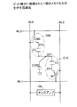
図16に基準電圧発生回路104の具体例を示す。基準電圧発生部104Bと基準電圧駆動部104Dとで構成される。基準電圧発生部104Bは、PMOSトランジスタM6を介して電源電圧VDDに接続されたダイオード接続のNMOSトランジスタM7と、NMOSトランジスタM9を介して接地電位GNDに接続されたダイオード接続のPMOSトランジスタM8とのソース端子同士が接続される。この構成によりトランジスタM7、M8のドレイン端子電圧は電源電圧VDDによらず一定のバイアス電圧を出力する。このバイアス電圧は、基準電圧駆動部104Dを構成するNMOSトランジスタM10及びPMOSトランジスタM11のゲート端子に入力される。トランジスタM10とM11のソース端子間が接続されて出力端子を構成するが、トランジスタM10とM11が各々ソースフォロアとして出力端子を基準電圧に維持する働きをする。尚、出力端子には基準電圧の補償素子として抵抗素子R1、R2を接続してもよい。
【0011】
図17は、メモリセルユニットU(図15、参照)を示す。1対のメモリセルC00とC10で構成されており、各々のメモリセルC00、C10は、セルキャパシタC0、C1がワード線WL0、WL1で制御されるNMOSトランジスタM0、M1を介してビット線BL0、/BL0に接続される。一般的にNMOSトランジスタM0、M1をトランファゲートと称する。トランスファゲートを介して、セルキャパシタC0、C1の一方の端子である電荷蓄積ノードST0、ST1とビット線BL0、/BL0との蓄積電荷の授受を行うことによりデータを記憶する。セルキャパシタC0、C1の他方の端子は、共通に接続されセルプレートCP1として基準電圧発生回路104により基準電圧VCPにバイアスされる。セルプレートCP1は、セルキャパシタC0、C1への電荷蓄積のための基準電圧となっているので、セルブロックB1内で共通電位となっており、有意な値の寄生容量としてCCP0が付加される。この寄生容量の全セルブロックB1乃至Bkについての総和が図15に示すセルプレート寄生容量CCPである。
【0012】
図18にメモリセルC00の断面図を示す。断面構造は全てのメモリセルで同一であるが、図18ではメモリセルC00に代表して付番する。ワード線WL0で制御されるNMOSトランジスタM0のドレイン端子が蓄積電荷ST0である。蓄積電荷ST0はセルキャパシタC0の一方の端子を構成しており、誘電体膜17を介してセルプレートCP1が配置されセルキャパシタC0を構成する。セルプレートCP1は、右方に延長されており、隣接するメモリセルのセルプレートCP1を介してセルブロックB1内の全てのセルキャパシタに共通に構成される。セルプレートCP1は、上層層間膜としてPSG膜19で保護され、メモリセル間においては窒化膜15上に形成される。これらの層間膜15、19との間に寄生容量成分が存在するため、セルプレートCP1として寄生容量CCP0が付加され、DRAM1000全体としてセルプレート寄生容量CCPとなる。
【0013】
アクセス動作は、データ読み出し・書き込み、及びリフレッシュの各々について、センスアンプ回路による差動増幅動作までは同様に行われる。即ち、行アドレスに対応するワード線WL0乃至WLnにより選択されたメモリセルC00乃至Cnmは、蓄積ノードがビット線BL0乃至/BLmに接続される。読み出された蓄積電荷は、ビット線対の微小電荷となり、これをセンスアンプ回路が差動増幅する。差動増幅によりデータの読み出し、あるいはリフレッシュが行われる(書込み動作については、この後に外部からの書き込みでデータを強制的に反転する。)。
【0014】
ここで、セルキャパシタC0、C1の蓄積ノードST0、ST1における急峻な電位変動が2回発生する。1回目は、蓄積ノードST0、ST1がビット線BL0乃至/BLmに接続される際である。セルキャパシタ容量に対してビット線容量が大きいため、接続時に蓄積電荷の再分配が行われ、蓄積ノードST0、ST1の電位は、略接地電位GNDあるいは内部降圧電圧Viicから、ビット線のイコライズ電圧であるVPR(略1/2・Viic)付近まで変化する。この変化はセルキャパシタC0、C1を介してセルプレートCP1に容量結合されて伝えられ、セルプレートCP1における寄生容量と合わせ電荷の分配が行われてセルプレート電位VCPを変動させる。しかしセンスアンプ回路が起動し差動増幅が行われると、ビット線電位は、1/2・ViicからGNDあるいはViic電位にリストアされる。この電位変動も同様にセルプレートCP1に容量結合されてセルプレート電位VCPを変動させる。これらの容量結合による電位変動は互いに逆方向であり両者は対となって印加されるので、結果的にセルプレート電位VCPに変動はない。
【0015】
【発明が解決しようとする課題】
しかしながら、電源投入時には、蓄積電荷はなく全てのセルキャパシタの蓄積ノードには蓄積電荷は存在しないかあっても微小である。この時のアクセス動作により以下に詳述する問題が発生する虞がある。
【0016】
図19に示すとおり電源投入と共に電源電圧VDDが上昇する。電源電圧VDDの上昇に従い基準電圧発生回路104が動作を開始してビット線電位VPR及びセルプレート電位VCPが1/2・Viicまで上昇する。この時セルプレート電位VCPからセルキャパシタC0、C1を構成する蓄積ノードST0、ST1への容量結合により電荷が注入される。注入された電荷は蓄積ノードST0、ST1における接合容量やゲート容量にも再分配されるため、蓄積ノードST0、ST1の電位VSTは、1/2・Viicより若干低い電位となる。
【0017】
この状態で、リフレッシュ動作等のアクセス動作が行われると、ワード線WLが活性化されて蓄積ノードST0、ST1とビット線BL0乃至/BLmが接続される。この時ビット線電位はVPR(=1/2・Viic)にイコライズされており、蓄積ノードST0、ST1の電位VSTにほぼ等しく電荷の移動は僅かであるため蓄積ノードST0、ST1はほぼ同電位を保持する。ここでダミーワード線DWLが活性化されるに伴い、ビット線BL0乃至/BLmがダミーキャパシタDC00乃至DC1mを介して容量結合を受け電荷の注入が行われるため、蓄積ノードST0、ST1の電位VSTは1/2・Viicより若干上昇する。この電位関係においてセンスアンプ回路が起動すると、蓄積ノードST0、ST1の電位VSTは内部降圧電圧Viicレベルまで上昇する。この電位上昇は、セルキャパシタC0、C1を介して容量結合によりセルプレートCP1に電荷供給を行いセルプレート電位VCPを上昇させる。尚、詳細な説明は省略するが、ダミーワード線DWLがない構成では、ビット線BL0乃至/BLmは接地電位GNDにリストアされ、セルプレート電位VCPは負側に容量結合を受ける。電位方向を反対にすれば以下の説明と同様な動作を行い同様な問題を有する。以下の説明は、ダミーワード線DWLの存在のもとでセルプレート電位VCPが上昇する場合についてのものである。
【0018】
セルプレート電位VCPが回復しないうちに順次ワード線WL0乃至WLnが選択されて上記の動作が繰り返されると、センスアンプ回路の活性化の度に発生する容量結合によるセルプレート電位VCPの上昇が蓄積し、最終的には内部降圧電圧Viicのレベルまで上昇してしまう虞がある。この現象は一回の動作でリストアされるメモリセルC00乃至Cnmの数が多いほど顕著に現れる。通常のアクセス動作に比して選択されるワード線WL0乃至WLnの数が多いリフレッシュ動作が代表的な場合である。セルキャパシタ容量を増加できない中で大容量化が進展する状況においてリフレッシュ周期を維持するためには、一回のリフレッシュ動作において選択されるメモリセルC00乃至Cnmの数は増加するので、今後の大容量化に伴い顕著に発生する虞がある。但し、発生原因はこれに留まるものではなく、アドレッシング等のアーキテクチャ構成やプロセステクノロジに依存する各容量成分の分布の仕方によっては、大容量化は条件とならず、また通常アクセスにおいても発生する可能性がある。
【0019】
こうした現象が、電源投入直後に“0”データの書込みを行ったメモリセルC00乃至Cnmの存在のもとに発生すると、セルプレートCP1の電位上昇に伴って、“0”データ書込み済みの蓄積ノードST0、ST1にもセルプレートCP1からの容量結合により電荷が供給されてしまい、蓄積ノードの電位VSTが上昇してしまう。この電位が1/2・Viicを越えて上昇するとこのメモリセルC00乃至Cnmから“0”データの読み出しができなくなり、データ化けが発生してしまい問題である。
【0020】
また、セルプレートCP1の電位が上昇している状態で、メモリセルC00乃至Cnmに1データを書き込んだ場合には、電荷蓄積ノードST0、ST1に充分な正の電荷が蓄積されないため、データ消失等が発生してしまう虞があり問題である。
【0021】
また、セルプレート電位VCPが最大で内部降圧電圧Viicまで上昇する虞がある。この後に0データを書き込むと、セルキャパシタC0、C1の端子間の誘電体膜17(図18、参照)に過大な電界ストレスが印加されることとなる。デバイスの信頼性に悪影響を及ぼすこととなり問題である。
【0022】
この状態を回避するためには、容量結合により供給された電荷を基準電圧発生回路104が吸収することが必要となる。そこで、基準電圧発生回路104の駆動能力を十分に大きくすることが考えられる。しかしながら、この方策では、基準電圧発生回路104での消費電流が増大してしまい低消費電流動作の要求に反するため実現することはできない。また回路規模も大きくならざるを得ず、チップ面積上の制約からも実現は困難である。
【0023】
また、大容量化に伴い多数のメモリセルC00乃至Cnmを配置するようになり、前述したようにセルブロックB1乃至Bkの配置領域は広大となる。VCP線の総配線長は長大となり、配線経路上の寄生抵抗RCP0乃至RCPkがセルプレート寄生容量CCPと組み合わされ遅延回路を形成してしまう。基準電圧発生回路104の駆動能力にも拘らず容量結合により生じた電荷の吸収を阻むこととなる。
【0024】
本発明は前記従来技術の問題点を解消するためになされたものであり、メモリセルに電荷蓄積用のセルキャパシタを備え、電荷の蓄積よりデータ記憶を行なう半導体記憶装置において、電源投入時において、全てのセルキャパシタの電荷蓄積ノードには蓄積電荷は存在しないかあっても微小である状態からアクセス動作に移行する場合おいても、セルプレート電位が変動しない半導体記憶装置を提供することを目的とする。
【0025】
【課題を解決するための手段】
前記目的を達成するために、請求項1に係る半導体記憶装置は、容量素子に電荷を蓄積することによりデータを記憶する複数の記憶セルを備え、各容量素子の第1端子を共通に接続して基準端子とすると共に、電荷の蓄積を、各容量素子の第2端子への電荷の注入・放出により行う半導体記憶装置において、基準端子に接続され、各容量素子の第2端子への電荷の注入・放出の際に各容量素子により容量結合されて注入される電荷に伴う基準電圧の電位変動を抑制する電位変動抑制容量素子と、基準端子と電位変動抑制容量素子とを接続する容量接続スイッチ素子と、電源電圧の投入を検知する電源検知回路とを備え、電源検知回路による検知に基づき生成される、所定パルス幅のパルス信号により計時される所定期間、容量接続スイッチ素子を導通して、基準端子と電位変動抑制容量素子とを電気的に接続することを特徴とする。
【0026】
そして、請求項2に係る半導体記憶装置は、請求項1に記載の半導体記憶装置において、各容量素子の第2端子への電荷の注入・放出の経路として所定数の記憶セル毎に設けられる複数のデータ線と、各データ線に基準電圧を供給する第1配線と、基準端子に基準電圧を供給する第2配線と、第1配線と第2配線とを接続する配線接続スイッチ素子と、電源電圧の投入を検知する電源検知回路とを備えており、電源検知回路からの信号に基づき、配線接続スイッチ素子を接続制御することを特徴とする。
【0027】
請求項1の半導体記憶装置では、電源検知回路による検知に基づき生成される、所定パルス幅のパルス信号により計時される所定期間、容量接続スイッチ素子が導通して、基準端子と電位変動抑制容量素子とが電気的に接続される。このとき各容量素子の第2端子に注入・放出される電荷に伴い容量結合されて基準端子に注入される電荷による基準電圧の電位変動を抑制する。
【0028】
請求項2の半導体記憶装置では、第1配線及び第2配線を介して、所定数の記憶セルが接続される複数のデータ線及び基準端子に基準電圧を供給している。電源検知回路からの信号に基づいて、配線接続スイッチ素子により第1配線と第2配線とを接続する。
【0029】
これにより、電源投入時に、電荷が蓄積されておらず0データも1データも存在しない記憶セルの容量素子に電荷を注入あるいは放出する場合に、容量素子の第2端子から基準端子への容量結合により移動する電荷が存在しても、電位変動抑制容量素子の存在により、あるいは複数のデータ線で総和される配線容量が接続されることにより、基準端子に供給される基準電圧の電位変動を抑制することができる。
【0030】
また、第1配線と第2配線を接続することにより、基準端子への配線抵抗を低減することができるので、基準電圧の発生回路の駆動能力を充分有効に活用することができ、容量結合により移動する電荷を有効に吸収して基準端子に供給される基準電圧の電位変動を抑制することができる。
【0031】
また、第1配線と第2配線との接続は電源投入時に限定することができるので、第1配線と第2配線とを分けることにより両者の独立性を維持してノイズ等による相互干渉を排除したり、試験時に個々に異なる電圧を印加できるという従来からの効果を有したまま、電源投入時における基準端子に供給される基準電圧の電位変動を抑制することができる。
【0032】
これらの手段により、電源投入時に、書き込まれたデータのデータ化けや消失を有効に防止することができ、容量素子の端子間の誘電体膜に過大電界ストレスが印加されることがなく信頼性上問題となる動作は発生しない。そして、これらの効果を実現するために、基準電圧の発生回路の駆動能力を必要以上に大きくする必要がないため、消費電流増大の負担やチップ占有面積増大の負担も最小限に抑制することができる。
【0033】
また、請求項3に係る半導体記憶装置は、請求項1に記載の半導体記憶装置において、基準端子に供給すべき基準電圧値信号を生成する基準電圧発生部と、複数の記憶セルのうち所定数の記憶セル毎に配置され、基準電圧値信号を受けて、基準電圧を所定数の記憶セルにおける基準端子の対応部分に供給する複数の基準電圧駆動部とを備えることを特徴とする。
【0034】
請求項3の半導体記憶装置では、複数の記憶セルのうち所定数の記憶セル毎に基準端子の対応部分に各々に配置される基準電圧駆動部から基準電圧を供給する。基準電圧駆動部から出力される基準電圧は、基準電圧発生部で生成される基準電圧値信号に応じて設定される。
【0035】
これにより、基準電圧の発生回路を、1つの基準電圧発生部と複数の基準電圧駆動部に分割して構成する。基準電圧発生部から基準電圧駆動部へ接続される基準電圧値信号は、電圧バイアス信号であるため入力インピーダンスを高く設定でき長い配線長を引き回しても大きな電位差は発生しないので、基準電圧駆動部を、駆動すべき基準端子の近傍に配置することができる。基準電圧駆動部と基準端子の間に配線抵抗、配線容量等の負荷が介在しないので、基準端子の電位を効果的に保持でき、基準端子の電位変動を抑制することができる。
【0036】
また、個々の基準電圧駆動部が駆動すべき基準端子は、所定数の記憶セル毎の対応部分に限定されるので、駆動すべき負荷を小さくすることができ、基準電圧駆動部の駆動能力を小さく抑えることができる。従って、基準電圧駆動部の回路規模を小さく設定することにより、チップ上の占有面積を必要最小限にすることができる。
【0037】
また、請求項4に係る半導体記憶装置は、容量素子に電荷を蓄積することによりデータを記憶する複数の記憶セルを備え、各容量素子の第1端子を共通に接続して基準端子とすると共に、電荷の蓄積を、各容量素子の第2端子への電荷の注入・放出により行う半導体記憶装置において、電源電圧の投入を検知する電源検知回路を備え、電源検知回路からの信号に基づき、電荷が注入される容量素子の第2端子を有する記憶セルと、電荷が放出される容量素子の第2端子を有する記憶セルとが同数であることを特徴とする。
【0038】
また、請求項5に係る半導体記憶装置は、請求項4に記載の半導体記憶装置において、各容量素子の第2端子への電荷の注入・放出の経路として所定数の記憶セル毎に設けられる複数のデータ線と、各データ線を2本で1対のデータ線対として接続してデータ線対の電位差を差動増幅する複数のセンスアンプ回路と、各データ線と各容量素子の第2端子とを電気的に接続する複数の選択線とを備え、電源検知回路からの信号に基づき、選択される所定数の選択線により、所定数のデータ線対を構成する各データ線に同数の容量素子の第2端子を電気的に接続することを特徴とする。
【0039】
また、請求項6に係る半導体記憶装置は、請求項4に記載の半導体記憶装置において、各容量素子の第2端子への電荷の注入・放出の経路として所定数の記憶セル毎に設けられる複数のデータ線と、各データ線と各容量素子の第2端子とを電気的に接続する複数の選択線と、各容量素子の第2端子から蓄積電荷が各データ線に放出された際、各データ線に電荷を追加補充する複数のダミー選択線と、各ダミー選択線の論理レベルを選択的に反転する反転選択回路とを備え、電源検知回路からの信号に基づき、選択される所定数の選択線及びダミー選択線により、所定数の容量素子の第2端子に電荷を注入・放出する際、各ダミー選択線のうちの半分を反転選択回路により論理反転することを特徴とする。
【0040】
また、請求項7に係る半導体記憶装置は、請求項4乃至6の少なくとも何れか1項に記載の半導体記憶装置において、複数の記憶セルのうち所定数の記憶セルを一単位として纏めたセルブロックを複数備え、電源検知回路からの信号に基づく動作は、各セルブロック単位で行なわれることを特徴とする。
【0041】
請求項4の半導体記憶装置では、電源検知回路からの信号によって、電荷が注入される記憶セルの数と電荷が放出される記憶セルの数とが同数となる。
【0042】
請求項5の半導体記憶装置では、電源検知回路からの信号によって、所定数の記憶セルが接続される複数のデータ線と各記憶セルの容量素子とを電気的に接続する複数の選択線が活性化し、センスアンプ回路に接続され対をなす所定数のデータ線対を構成するデータ線毎に同数の容量素子を接続する。
【0043】
請求項6の半導体記憶装置では、電源検知回路からの信号によって、所定数の記憶セルが接続される複数のデータ線と各記憶セルの容量素子とを電気的に接続する複数の選択線が活性化する。更に各データ線に放出された電荷を追加補充する各ダミー選択線も合わせて活性化する。この時、各ダミー選択線の半分について論理レベルを反転して各データ線に反転した電荷の追加補充を行なう。
【0044】
請求項7の半導体記憶装置では、複数の記憶セルのうち所定数の記憶セルを一単位として纏めたセルブロック単位で電源検知回路からの信号に基づく動作を行なう。
【0045】
これにより、電荷が注入される記憶セルと電荷が放出される記憶セルとが対となるので、容量素子を介して基準端子に容量結合する電荷は相殺され、基準端子における電位変動を抑制することができる。
【0046】
この記憶セルの対は、センスアンプ回路に接続され対をなすデータ線対を構成する各データ線に対して同数の記憶セルを選択してやれば、書き込みデータの選択を意識的に行なう必要なく、電荷注入と電荷放出の記憶セルをセンスアンプ回路に接続されるデータ線対の間で同数とし、容量素子の第2端子と基準端子との間の移動電荷を相殺して基準端子の電位変動を抑制することができる。
【0047】
また、各データ線に放出された電荷を追加補充するダミー選択線を使用する場合は、ダミー選択線の半分について論理レベルを反転してやれば、書き込みデータの選択を意識的に行なう必要はなく、電荷注入される容量素子と電荷放出される容量素子とを同数に設定して、容量素子の第2端子と基準端子との間の移動電荷を相殺して基準端子の電位変動を抑制することができる。
【0048】
また、この移動電荷の相殺動作を、所定数の記憶セルを一単位として纏めたセルブロック単位で行なえば、電荷注入と電荷放出との記憶セルが比較的近接するため、移動電荷を効率的に相殺することができる。
【0049】
また、請求項8に係る半導体記憶装置は、容量素子に電荷を蓄積することによりデータを記憶する複数の記憶セルを備え、各容量素子の第1端子を共通に接続して基準端子とすると共に、電荷の蓄積を、各容量素子の第2端子への電荷の注入・放出により行う半導体記憶装置において、各容量素子の第2端子への電荷の注入・放出の経路として所定数の記憶セル毎に設けられる複数のデータ線と、各データ線に基準電圧を供給する第1配線と、基準端子に基準電圧を供給する第2配線と、第1配線あるいは第2配線と所定電圧との間に設けられたクランプスイッチ素子と、各データ線と各容量素子の第2端子とを電気的に接続する複数の選択線と、電源電圧の投入を検知する電源検知回路とを備え、電源検知回路からの信号に基づき、クランプスイッチ素子を制御して第1配線あるいは第2配線を所定電圧に固定し、所定数の選択線を選択して各容量素子の第2端子を設定電圧にし、更に所定数の選択線を非選択とした後、クランプスイッチ素子を制御して第1配線あるいは第2配線から所定電位を切り離し、基準電圧を供給することを特徴とする。
【0050】
また、請求項9に係る半導体記憶装置は、請求項8に記載の半導体記憶装置において、所定電圧は、容量素子の第2端子におけるハイレベル電圧あるいはローレベル電圧であり、基準電圧は、ハイレベル電圧とローレベル電圧との相加平均電圧であり、第1配線が所定電圧に固定される場合、設定電圧は所定電圧であり、所定数の選択線を非選択とした後も各容量素子の第2端子は設定電圧を保持し、第2配線が所定電圧のうちハイレベル電圧あるいはローレベル電圧の一方の電圧に固定される場合、設定電圧は基準電圧となり、所定数の選択線を非選択とした後は、第2配線が基準電圧となる際、基準端子からの容量結合により、各容量素子の第2端子は所定電圧のうちハイレベル電圧あるいはローレベル電圧の他方の電圧となることを特徴とする。
【0051】
請求項8の半導体記憶装置では、第1配線及び第2配線を介して、所定数の記憶セルが接続される複数のデータ線及び基準端子に基準電圧を供給する。電源検知回路からの信号に基づいて、クランプスイッチ素子により、第1あるいは第2配線は所定電圧に固定される。所定数の記憶セルを接続する複数のデータ線と各容量素子とを電気的に接続する複数の選択線が選択されて各容量素子の第2端子を設定電圧にした後、所定数の選択線を非選択としクランプスイッチ素子を制御して第1あるいは第2配線から所定電位を切り離し基準電圧を供給する。
【0052】
請求項9の半導体記憶装置では、第1及び第2配線を介して、データ線及び基準端子に基準電圧として容量素子におけるハイレベル電圧とローレベル電圧との相加平均電圧を供給している。電源検知回路からの信号に基づいて、第1あるいは第2配線はハイレベル電圧あるいはローレベル電圧に固定される。クランプスイッチ素子により、第1配線がハイレベル電圧あるいはローレベル電圧に固定される場合は、各容量素子の第2端子もハイレベル電圧あるいはローレベル電圧となり、この電圧は選択線を非選択とした後も保持される。第2配線がハイレベル電圧あるいはローレベル電圧に固定される場合は、各容量素子の第2端子は基準電圧である相加平均電圧となり、この電圧は選択線を非選択とした後は、第2配線が基準電圧となる際、基準端子からの容量結合によりローレベル電圧あるいはハイレベル電圧となる。これは選択線の選択前の第2配線の電圧とは反対の関係である。第1あるいは第2配線は基準電圧となる。
【0053】
これにより、第1配線を所定電圧に固定すれば所定数の選択線を選択するだけで所定数の容量素子の第2端子をデータ書き込み状態の電荷蓄積状態にすることができる。この電荷蓄積状態への移行は、センスアンプ回路による差動増幅動作等を行う必要はなく、所定数の選択線の選択も1サイクルで行なうこともでき移行動作は短時間とすることができる。従って、容量素子の第2端子への電荷の注入・放出に伴う基準端子の電位変動が収まるまでの時間を充分に確保することができる。
【0054】
また第2配線を所定電圧に固定すれば所定数の選択線を選択することにより所定数の容量素子の第2端子を基準電圧レベルの電荷蓄積状態にした後、第2配線の固定を解除して正規の電圧に移行する際、容量素子を介しての容量結合により容量素子の第2端子をデータ書き込み状態の電荷蓄積状態にすることができる。この電荷蓄積状態への移行は、基準端子が固定された所定電圧から正規の電圧に移行する際の容量素子を介しての容量結合を利用して行なわれる。従って、容量結合に伴う電荷移動が容量素子の第2端子及び基準端子の電位変動を誘発することなく、更に容量素子の第2端子への電荷注入・放出に利用されてデータ書き込みを補助する効果を奏する。
【0055】
何れの場合も、センスアンプ回路による差動増幅動作等を行う必要はなく、所定数の選択線の選択も1サイクルで行なうこともでき、短時間でデータ書き込みを完了することができる。そして選択線の選択動作は、既存の回路を有効に流用することができ、更に試験回路等の回路をそのまま流用することもできる。
【0056】
【発明の実施の形態】
以下、本発明の半導体記憶装置について具体化した第1乃至第7実施形態を図1乃至図14に基づき図面を参照しつつ詳細に説明する。図1は、第1実施形態の半導体記憶装置を示す回路ブロック図である。図2は、第1実施形態の効果を示す説明図である。図3は、第2実施形態の半導体記憶装置を示す回路ブロック図である。図4は、第3実施形態の半導体記憶装置を示す回路ブロック図である。図5は、第3実施形態の半導体記憶装置の動作を示す波形図である。図6は、第3実施形態の半導体記憶装置の動作を示す回路図である。図7は、第4実施形態の半導体記憶装置を示す回路ブロック図である。図8は、ダミーセルの例を示す回路図である。図9は、第4実施形態の半導体記憶装置の動作を示す波形図である。図10は、第5実施形態の半導体記憶装置を示す回路ブロック図である。第11図は、第5実施形態の半導体記憶装置の動作を示す波形図である。図12は、第6実施形態の半導体記憶装置を示す回路ブロック図である。図13は、第6実施形態の半導体記憶装置の動作を示す波形図である。第14図は、第7実施形態の半導体記憶装置を示す回路ブロック図である。
【0057】
図1に示す第1実施形態の半導体記憶装置1(以下、DRAM1と称する。)は、従来技術のDRAM1000(図15、参照)に加えて、基準電圧発生回路104からの基準電圧VPR、VCPの供給線であるVPR線、VCP線について、各セルブロックB1乃至Bk毎に両線を接続するNMOSトランジスタM1乃至Mkを備える。NMOSトランジスタM1乃至Mkのゲート端子は共通に信号φCPRに接続される。ここで、φCPRは電源投入後の所定時間に正の論理レベルを出力する信号である。φCPR信号を生成する回路として、電源投入を検知して所定期間のパルス信号を出力するパワーオンリセット回路の出力信号を利用することができる。またこの信号を受けて、パワーオンリセット信号のパルス幅を所定時間に拡張する回路として、パルス信号の終端エッジに対してのみ遅延する応答特性をもった回路を付加することも可能である。
【0058】
大容量DRAM1においては、セルブロックB1乃至Bkの配置領域は広大であるため各供給線(VPR線、VCP線)の総配線長は長大となり配線経路上に寄生抵抗RPR0乃至RPRk、RCP0乃至RCPkが存在する。従って、各セルブロックB1乃至Bk毎にVPR線とVCP線とを短絡するNMOSトランジスタM1乃至Mkを備えることにより、電源投入時に、両配線が各セルブロックB1乃至Bk毎に短絡される。
【0059】
また、各ビット線BL0乃至/BLmには、トランスファゲートを介して多数のメモリセルC00乃至Cnmが接続されている。トランスファゲートはNMOSトランジスタで構成されており、そのドレイン端子がビット線BL0乃至/BLmに接続されている。そのため、ビット線BL0乃至/BLmには多数の接合容量が付加されることとなる。更に大容量DRAM1においては、ビット線BL0乃至/BLm間の距離やワード線WL0乃至WLnとの交差距離が共に近接しているため、線間容量も大きなものとならざるを得ず、個々のビット線BL0乃至/BLmの配線容量CBL、CBBL(図2、参照)は大きなものとなる。
そして図2に示すように、この配線容量CBL、CBBLがビット線イコライズ時に全てのビット線BL0乃至/BLmについて加算されてビット線イコライズ容量CPRが形成される。ビット線イコライズ容量CPRは、セルプレート寄生容量CCPに比して無視できない大きさとなる。またセルプレート寄生容量CCPは、各メモリセルユニットUにおけるセルプレートCP1に付加する寄生容量CCP1の総和である。
【0060】
第1実施形態のDRAM1では、電源投入時に、電荷が蓄積されておらず“0”データも“1”データも存在しないメモリセルC00乃至Cnmの容量素子に電荷を注入あるいは放出する場合に、第2端子である電荷蓄積ノードから基準端子であるセルプレートCP1への容量結合により移動する電荷が存在しても、複数のデータ線であるビット線BL0乃至/BLmで総和される配線容量であるビット線イコライズ容量CPRが接続されることにより、セルプレートCP1の電位変動を抑制することができる。この時、ビット線イコライズ容量CPRは、セルブロックB1乃至Bk毎に分轄して配置されるので、個々のビット線イコライズ容量CPRに付加される寄生抵抗は大きなものとはならず、容量成分との組み合わせで不要な遅延成分が付加されることはない。ビット線イコライズ容量CPRに代えて、電位変動抑制容量素子をセルプレートCP1に接続しても、同様の効果を奏することができる。
【0061】
また、第1配線であるVPR線と第2配線であるVCP線とを接続することにより、基準電圧発生回路104とセルプレートCP1との間の配線抵抗を低減することができるので、基準電圧発生回路104の駆動能力を充分有効に活用することができ、容量結合により移動する電荷を有効に吸収してセルプレートCP1の電位変動を抑制することができる。
【0062】
また、VPR線とVCP線との接続は電源投入時に限定することができるので、VPR線とVCP線とを分けることにより両者の独立性を維持してノイズ等による相互干渉を排除したり、試験時に個々に異なる電圧を印加できるという従来からの効果を有したまま、電源投入時におけるセルプレートCP1の電位変動を抑制することができる。
【0063】
これらの効果により、電源投入時に、書き込みデータのデータ化けや消失を有効に防止することができ、容量素子であるセルキャパシタC0、C1の端子間の誘電体膜17に過大電界ストレスが印加されることがなく信頼性上問題となる動作は発生しない。そして、これらの効果を実現するために、基準電圧発生回路104の駆動能力を必要以上に大きくする必要がないため、消費電流増大の負担やチップ占有面積増大の負担も最小限に抑制することができる。
【0064】
尚、電位変動抑制容量素子とセルプレートCP1との接続を、容量接続スイッチ素子により、電源投入時に限定して行うように構成することも可能である。これにより、通常動作時においてセルプレートCP1に電位変動抑制容量素子を付加することなく、電源投入時においてのみ付加してセルプレートCP1の電位変動を抑制することができる。
【0065】
また、電位変動抑制容量素子をセルブロックB1乃至Bk毎に分割して配置することもできる。これにより、ビット線イコライズ容量CPRの場合と同様に、個々の電位変動抑制容量成分に付加される寄生抵抗は大きなものとはならず、容量成分との組み合わせで不要な遅延成分が付加されることはない。
【0066】
また、電位変動抑制容量素子、容量接続スイッチ素子、あるいは配線接続スイッチ素子M1乃至Mkは、セルブロックB1乃至Bkが配置されている記憶セル領域であるメモリセル領域に配置することができる。例えば、電位変動抑制容量素子は、メモリセルC00乃至Cnmのセルキャパシタを構成するセルプレートCP1の上に所定の酸化膜を介して導電性電極を形成してやればセルプレートCP1上に重ねて配置することができ、チップ上に特別に占有面積を確保する必要はない。また配線接続スイッチ素子M1乃至Mkは、セルブロックB1乃至Bk毎に1つ備えてやればよく、チップ上の占有面積は極僅かでありメモリセル領域を圧迫することなく配置できる。
【0067】
また、配線接続スイッチ素子M1乃至MkはNMOSトランジスタで例示したが、PMOSトランジスタで構成することもできる。またPMOS及びNMOSトランジスタをペア接続するいわゆるトランスミッションゲートやその他のスイッチング特性を奏する回路であれば適用することができる。容量接続スイッチ素子についても同様に、NMOSトランジスタ、PMOSトランジスタ、トランスミッションゲート、あるいはその他のスイッチング回路等で構成することができる。
【0068】
図3に示す第2実施形態の半導体記憶装置2(以下、DRAM2と称する。)では、従来技術のDRAM1000(図15、参照)における基準電圧発生回路104に代えて、基準電圧発生回路104の構成要素である基準電圧発生部104Bと基準電圧駆動部104D乃至104Dを分けて配置する。基準電圧駆動部104D乃至104Dは、セルブロックB1乃至Bk毎に分散して配置され、各々のセルブロックB1乃至BkにおけるセルプレートCP1乃至CP1にVCP電圧を供給する。基準電圧駆動部104Dは、基準電圧駆動部104D乃至104Dが出力すべき基準電圧を設定するための基準電圧値信号を出力する。MOSトランジスタM6及びM7の接続点、MOSトランジスタM8及びM9の接続点から出力される信号は、バイアス電圧信号として基準電圧駆動部104D乃至104DのNMOSトランジスタM10乃至M10、及びPMOSトランジスタM11乃至M11の各ゲート端子に入力される。
【0069】
また、従来技術のDRAM1000におけるNMOSトランジスタMPR、MCPに代えて、各基準電圧駆動部104D乃至104Dの出力を分轄して、NMOSトランジスタMPR1乃至MPRk、及びMCP1乃至MCPkを介してビット線BL0〜/BLm乃至BL0〜/BLm、及びセルプレートCP1乃至CP1に接続して、それぞれを独立にバイアスするように設定することも可能である。
【0070】
第2実施形態のDRAM2では、基準電圧発生回路を、基準電圧発生部104Bと基準電圧駆動部104D乃至104Dに分割する。基準電圧発生部104Bから基準電圧駆動部104D乃至104Dへ接続される基準電圧値信号は、電圧バイアス信号であるため高い入力インピーダンスのMOSトランジスタM10乃至M10、M11乃至M11に設定すれば、長い配線長を引き回しても大きな電位差は発生しない。そのため基準電圧駆動部104D乃至104DをセルプレートCP1乃至CP1の近傍に配置することができる。基準電圧駆動部104D乃至104DとセルプレートCP1乃至CP1の間に配線抵抗、配線容量等の負荷が介在しないので、セルプレートCP1乃至CP1の電位を効果的に保持でき、セルプレートCP1乃至CP1の電位変動を抑制することができる。
【0071】
また、個々の基準電圧駆動部104Dが駆動すべきセルプレートCP1は、セルブロックB1乃至Bk毎に限定されるので、駆動すべき負荷を小さくすることができ、基準電圧駆動部104D乃至104Dの駆動能力を小さく抑えることができる。従って、基準電圧駆動部104D乃至104Dの回路規模を小さく設定することにより、チップ上の占有面積を必要最低限にすることができる。ビット線BL0〜/BLm乃至BL0〜/BLm、及びセルプレートCP1乃至CP1を各々独立にバイアスするために設置するNMOSトランジスタMPR1乃至MPRk、及びMCP1乃至MCPkの素子サイズも、基準電圧駆動部104D乃至104Dが駆動すべき負荷がセルブロックB1乃至Bk毎に限定されているので、小さく設定することができる。
【0072】
尚、基準電圧駆動部104D乃至104Dは、セルブロックB1乃至Bkが配置されている記憶セル領域であるメモリセル領域に配置することができる。セルブロックB1乃至Bk毎のセルプレートCP1のみに限定して駆動できればよいので、個々の基準電圧駆動部104Dは限定された駆動能力でよく、従って回路規模も小さくなりチップ上の占有面積は極僅かでありメモリセル領域を圧迫することなく配置できる。
【0073】
また、NMOSトランジスタMPR1乃至MPRk、及びMCP1乃至MCPkは、PMOSトランジスタで構成することもできる。またPMOS及びNMOSトランジスタをペア接続するいわゆるトランスミッションゲートやその他のスイッチング特性を奏する回路であれば適用することができる。
【0074】
図4に示す第3実施形態の半導体記憶装置3(以下、DRAM3と称する。)では、従来技術のDRAM1000(図15、参照)に加えて、電源電圧の投入を検知する電源検知回路105と、電源検知回路105からのパルス出力信号PORのパルス幅を拡張するパルス拡張回路70と、パルス拡張回路70からの出力信号φYを受けて動作する制御回路80を備える。制御回路80はワード線活性化信号φXと共に、センスアンプ群活性化信号LEを出力する。両信号は各セルブロックB1乃至Bkに出力される。電源検知回路105、パルス拡張回路70は既存の回路を利用することができる。例えば、電源検知回路105は、パワーオンリセット回路であり、出力信号として電源投入時に正のパルス信号PORを出力する。またパルス拡張回路70は、正の入力パルス信号PORに対して終端のパルスエッジであるフォールエッジにのみ遅延を付加する回路である。出力信号として入力パルス信号PORの終端側にパルス幅が拡張された拡張パルス信号φYを出力する。
【0075】
次に、電源起動時における回路動作を図5の波形図に基づき説明する。電源が投入され電源電圧VDDが立ち上がると、電源検知回路105から正のパルス信号PORが出力される。このパルス信号PORが入力されるパルス拡張回路70からは、正の拡張パルス信号φYが出力される。この拡張パルス信号φYは、パルス信号PORのフォールエッジを遅延させて終端側にパルス幅を拡張した信号である。拡張パルス信号φYは制御回路80に入力される。制御回路80からは、先ず、センスアンプ群活性化信号LEが出力される。この信号によりセンスアンプ群102に備えられる全てのセンスアンプ回路が一斉に活性化される。これにより、各センスアンプ回路に接続されているビット線対BL0と/BL0〜BLmと/BLmを差動増幅する。ビット線対毎のイコライズ電圧の差異、センスアンプ回路の感度差、差動増幅時の擾乱等の不確定要因により各ビット線対は差動増幅されることとなる。従って、ビット線対間の差動増幅方向は不確定である。
【0076】
ビット線対BL0と/BL0〜BLmと/BLmの差動増幅が完了するタイミングを待って、制御回路80はワード線活性化信号φXを出力してワードドライバ群101に備えられる全ワード線WL0〜WLnを一斉に選択する。ワード線が選択されると各メモリセルC00乃至CnmのトランスファーゲートM0、M1が導通し、セルキャパシタC0、C1の電荷蓄積ノードST0、ST1が各ビット線に接続される。この時点では、各ビット線対は差動増幅されているので、差動増幅の後の電圧が各セルキャパシタC0、C1に書き込まれることとなる(図5では、ST0に論理ハイレベル電圧、ST1に論理ローレベル電圧が書き込まれる場合を示す。)全てのビット線はセンスアンプ回路を挟んで対となっているので、差動増幅動作されたビット線対においては、論理ハイレベル電圧が書き込まれるセルキャパシタC0、C1の数と論理ローレベル電圧が書き込まれるセルキャパシタC0、C1の数とが同数となる。
【0077】
セルキャパシタC0、C1への書き込み終了後、拡張パルス信号φYの終了に伴い、制御回路80は、ワード線活性化信号φXを非活性としてワード線WL0〜WLnの選択を解除した後に、センスアンプ群活性化信号LEを解除して全センスアンプ回路を非活性としビット線対をイコライズして動作を完了する。この動作を電源投入から通常の動作が行われるまでの待機時間であるいわゆるポーズ時間内に実行する。
【0078】
第3実施形態のDRAM3では、電荷が注入されるメモリセルC00〜Cnmと電荷が放出されるメモリセルC00〜Cnmとが対となるので、セルキャパシタC0、C1を介してセルプレートCP1に容量結合する電荷は相殺され、セルプレートCP1における電位変動を抑制することができる。
【0079】
この様子を示したのが、図6である。センスアンプ回路106により差動増幅された電位差によりビット線対BL0と/BL0はリストアされる。今仮に、ビット線BL0が論理ハイレベル電圧に、ビット線/BL0が論理ローレベル電圧にリストアされているとする。この状態でワード線WL0、WL1が選択されると、トランスファゲートを構成するNMOSトランジスタM0、M1は共に導通して、メモリセルの電荷蓄積ノードST0、ST1をビット線BL0、/BL0に接続する。則ち、電荷蓄積ノードST0は論理ハイレベル電圧となり電荷が注入される。逆に電荷蓄積ノードST1は論理ローレベル電圧となり電荷が放出される。電荷蓄積ノードST0、ST1に電荷が注入・放出されると、セルキャパシタC0、C1を介して容量結合することによりセルプレートCP1に電荷が放出・注入される。具体的には、電荷蓄積ノードST0に注入された電荷によりセルキャパシタC0によりセルプレートCP1に電荷が注入される(これをΔC+とする。)。電荷蓄積ノードST1から放出された電荷によりセルキャパシタC1によりセルプレートCP1から電荷が放出される(これをΔC−とする。)。ここで、ワード線WL0、WL1選択前の電荷蓄積ノードST0、ST1の電位は、略ビット線対のイコライズ電圧と同じであり、この電圧はリストア時の論理ハイ・ローレベル電圧の相加平均値である。従って、両セルキャパシタC0、C1による容量結合の効果は略等しくなる(ΔC+=ΔC−)。従って、容量結合によりセルプレートCP1に注入・放出される電荷は相殺する。よって、セルプレートCP1に電位変動は発生しない。
【0080】
メモリセルユニットUにおけるメモリセルC00〜Cnmの対に接続されるビット線対BL0と/BL0〜BLmと/BLmから、ビット線毎に同数のメモリセルを選択してやれば、書き込みデータの選択を意識的に行なう必要なく、電荷注入と電荷放出のメモリセルの間の移動電荷を相殺してセルプレートCP1の電位変動を抑制することができる。
【0081】
尚、ワード線活性化信号φXでは一斉に全ワード線WL0〜WLnを選択し、センスアンプ群活性化信号LEでは、全センスアンプ回路を一斉に活性化し全ビット線対BL0と/BL0〜BLmと/BLmを一斉にリストアする場合を示した。この場合には、全てのメモリセルC00乃至Cnmにデータを書き込むこととなりその後のアクセス動作においてセルプレートCP1に電位変動が発生しない。しかしながら、セルプレートCP1の電位変動は、基準電圧発生回路104の駆動能力と容量結合とのバランスで決まる現象である。従って、基準電圧発生回路104が許せば全てを一斉に活性化する必要はなく、基準電圧発生回路104の駆動能力の範囲内で、活性化するワード線及びビット線対を一部に限定することもできる。
【0082】
また、上述の第3実施形態では、センスアンプ回路の活性化によるビット線対BL0と/BL0〜BLmと/BLmのリストアの後にワード線WL0乃至WLnを選択してビット線とセルキャパシタC0、C1とを接続してセルキャパシタC0、C1にリストア電圧を書き込むシーケンスを示した。しかしながら、書き込むべき電圧については論理ハイレベル電圧と論理ローレベル電圧で同数にするという制約があるだけである。従って、ビット線対における任意の差電圧をリストアして書き込めば条件を満足する。則ち、ワード線の選択タイミングとセンスアンプ回路の活性化タイミングとの間に時間的に重なり合う期間を設定してやれば両者の起動及び終了タイミングには特に制約を設けることなく自由に設定することができる。
【0083】
また、電源投入時の信号としては、上述の拡張パルス信号φYが利用できる他、パワーオンリセット回路等の電源検知回路105からの出力信号を直接使用することもできる。またパルス信号の論理としては、上述の正のパルスの他、負のパルスを使用することもできる。更にパワーオンリセット回路等の電源検知回路105からの出力信号はパルス信号である必要はなく、電源投入を検知することができれば、2値出力の信号であってもよい。
【0084】
また、第3実施形態における回路動作は、セルブロック単位で行うことが好ましい。これにより、容量結合により相互に反対方向に電荷の移動が発生するメモリセル同士が近接する位置に存在することとなり、移動電荷の相殺効果を向上させることが可能である。
【0085】
図7に示す第4実施形態の半導体記憶装置4(以下、DRAM4と称する。)では、第3実施形態のDRAM3(図4、参照)に加えて、制御回路80からの出力信号φXを受けて、活性化するワード線WL0〜WLnに対応してダミーワード線DWL0、DWL1の論理を反転制御する反転指示信号φIを出力する反転選択回路60と、反転指示信号φIを受けて、信号φXにより選択されるダミーワード線DWL0、DWL1を反転する反転スイッチ回路I1乃至Ikを備える。
【0086】
ここで、ダミーワード線DWL0、DWL1とは、センスアンプ群102に備えられるセンスアンプ回路の差動増幅動作を確実にするために、ビット線対BL0と/BL0乃至BLmと/BLmにダミーセルDC00乃至DC1mを介しての容量結合により電荷を追加供給するものである。本実施形態では、電荷を追加供給して各ビット線の電位を上昇させる情報“1”を読み易くするアシスト1効果を奏する構成である。
【0087】
図8には、具体的なダミーセル構成を示す。ここでは6種類のダミーセル構成を例示している。(1)は、ダミーワード線DWLによりトランスファゲートMを制御してセルキャパシタCMの容量値より少ない容量値を有するダミーセルキャパシタCM/2(この例では、半分の容量値を有する。)をビット線BL、/BLに接続する構成である。メモリセルの構成と同様な構成を有している。(2)は、ビット線BL、/BLとダミーワード線DWLとの間にダミーキャパシタDCを接続するものである。ダミーワード線DWLの起動により容量結合して電荷を供給する。(3)及び(4)は、NMOSトランジスタMNのゲート容量を利用する構成である。ゲート端子を、ビット線BL、/BLとダミーワード線DWLとの何れに接続するかで2つの構成がある。(5)及び(6)は、(3)及び(4)におけるNMOSトランジスタMNに代えて、PMOSトランジスタMPを使用する構成である。
【0088】
さて、電源起動時における回路動作を図9の波形図に基づき説明する。ここでは、図17のメモリセル対の回路図も併せて参考にしながら説明する。電源が投入され電源電圧VDDが立ち上がると、電源検知回路105から正のパルス信号PORが出力される。このパルス信号PORが入力されるパルス拡張回路70からは、正の拡張パルス信号φYが出力される。拡張パルス信号φYが入力される制御回路80からは、ワード線活性化信号φXとセンスアンプ群活性化信号LEとが出力される。
【0089】
先ず、ワード線活性化信号φXにより選択されるワード線WL0が立ち上がりトランスファゲートM0を導通して、電源起動時のセルプレートCP1からの容量結合により基準電圧(例えば、1/2・Viic)の近傍にまで昇圧されていた電荷蓄積ノードST0は、基準電圧(例えば、1/2・Viic)にイコライズされていたビット線BL0と接続する。その後ダミーワード線DWL0が選択されることにより、ビット線BL0にアシスト1効果が作用してビット線電位を上昇させ、ビット線/BL0との電位差を拡大してリストア動作を待つ。
【0090】
次に、センスアンプ群活性化信号LEが活性化して各センスアンプ回路が起動し、ビット線対BL0と/BL0をリストアすることにより、電荷蓄積ノードST0に1データが書き込まれる。則ち、電荷蓄積ノードST0に電荷が注入される。
【0091】
プリチャージ動作の後、ワード線活性化信号φXによりワード線WL1が選択され同様の動作を繰り返す。ただし、プリチャージ期間に出力信号φXを受けて反転選択回路60からダミーワード線DWL1の論理を反転制御する反転指示信号φIが出力されるので、反転スイッチ回路I1乃至Ikは、ワード線活性化信号φXからダミーワード線DWL1への経路に信号反転回路G9を付加する。
【0092】
従って、ダミーワード線DWL1の信号遷移の方向が反転されて、ビット線/BL0にビット線の電位を下降させて情報“0”を読み易くするアシスト0効果が作用してビット線電位を下降させ、電荷蓄積ノードST1には0データが書き込まれる。則ち、電荷蓄積ノードST1からは電荷が放出される。
【0093】
メモリセルの電荷蓄積ノードへの書き込みが、1データ書き込みと0データ書き込みとで同数となるようにダミーワード線の半分について、信号遷移の方向を反転して書き込み動作を繰り返す。
【0094】
第4実施形態のDRAM4では、電荷が注入されるメモリセルC00〜Cnmと電荷が放出されるメモリセルC00〜Cnmとが対となるので、セルキャパシタC0、C1を介してセルプレートCP1に容量結合する電荷は相殺され、セルプレートCP1における電位変動を抑制することができる。
【0095】
また、センスアンプ回路による差動増幅の動作余裕を向上させるためにダミーセルDC00乃至DC1mを使用する場合には、ダミーセルに容量結合するダミー選択線DWL0、DWL1の半分について論理レベルを反転する。これによりビット線BL0〜/BLmへのダミーセルを介してのアシスト1の電荷供給のうちの半分をアシスト0の電荷供給とすることができる。メモリセルC00乃至Cnmへの書き込みデータの選択を意識的に行なう必要はなく、電荷注入されるセルキャパシタC0、C1と電荷放出されるセルキャパシタC0、C1とを同数に設定して、電荷蓄積ノードST0、ST1とセルプレートCP1との間の移動電荷を相殺してセルプレートCP1の電位変動を抑制することができる。
【0096】
尚、第4実施形態では、相補なデータを書き込むメモリセルC00乃至Cnmの数については言及していないが、全てのメモリセルにデータを書き込めばその後のアクセス動作によってセルプレートCP1に電位変動が発生することはない。しかしながら、セルプレートCP1の電位変動は、基準電圧発生回路104の駆動能力と容量結合とのバランスで決まる現象である。従って、基準電圧発生回路104が許せば全メモリセルに書き込む必要はなく、基準電圧発生回路104の駆動能力の範囲内で、活性化するワード線及びビット線対を一部に限定することもできる。
【0097】
また、ワード線の選択とビット線の活性化との順序についても、上述の順番に限定されることはなく、アシスト1とアシスト0が同数になるようにしてリストアされたビット線対の差電圧を書き込めれば条件を満足する。則ち、ワード線の選択タイミングとセンスアンプ回路の活性化タイミングとの間に時間的に重なり合う期間を設定してやれば両者の起動及び終了タイミングには特に制約を設けることなく自由に設定することができる。
【0098】
更にワード線WL0乃至WLnとダミーワード線DWL0、DWL1との立ち上がり順序についても、上述のシーケンスに限定される必要はない。ダミーワード線によるアシスト1とアシスト0が設定できるタイミングであれば、ダミーワード線をワード線と同時に立ち上げても、先だって立ち上げてもよい。
【0099】
また、ダミーセルDC00乃至DC1mの容量値をセルキャパシタの容量値の半分として説明したが(図8、(1))、これに限定されるものではなく、アシスト動作が確実に行われれば、容量値は自由に設定することができる。
【0100】
また、第4実施形態における回路動作は、セルブロック単位で行うことが好ましい。これにより、容量結合により相互に反対方向に電荷の移動が発生するメモリセルC00乃至Cnm同士が、近接する位置に存在することとなり、移動電荷の相殺効果を向上させることが可能である。
【0101】
このほかにも、電荷が注入されるメモリセルC00乃至Cnmと放出されるメモリセルとが同数になるような方法であれば、容量結合によるセルキャパシタCP1への電荷の移動は相殺されて電位変動を抑えることができる。例えば、論理ハイレベル、即ち1データ、あるいは論理ローレベル、即ち0データで固定されたデータを、ビット線対BL0と/BL0乃至BLmと/BLmを構成する各ビット線に接続されているメモリセルを同数選択して書き込んでやれば、セルキャパシタC0、C1への電荷の注入と放出が同数となり同様の効果が得られる。
【0102】
図10に示す第5実施形態の半導体記憶装置5(以下、DRAM5と称する。)では、従来技術のDRAM1000(図15、参照)に加えて、第3実施形態のDRAM3における電源検知回路105と、パルス拡張回路70を備える。パルス拡張回路70からの拡張パルス信号φYは、ワードドライバ群101に入力される。またVCP線を接地電位GNDに固定するNMOSトランジスタ10のゲート端子に入力されると共にノアゲート9に入力される。ノアゲート9の他方の入力には、従来技術のDRAM1000においてNMOSトランジスタMCPのゲート端子に入力されていたコントロール信号φCPが入力される。
【0103】
電源投入時に出力される拡張パルス信号φYは、ワードドライバ群101を介して全てのワード線WL0〜WLnを選択する。またノアゲート9の出力信号をローレベルに固定することによりNMOSトランジスタMCPを非道通として、VCP線を基準電圧発生回路104から切り離すと共に、NMOSトランジスタ10により、VCP線を接地電位GNDレベルに固定する。
【0104】
電源起動時における回路動作は、図11の波形図に示すとおりである。以下の説明では、必要に応じて図17のメモリセル対の回路図を参考にする。則ち、電源が投入され電源電圧VDDが立ち上がると、電源検知回路105から正のパルス信号PORが出力される。このパルス信号PORが入力されるパルス拡張回路70からは、正の拡張パルス信号φYが出力される。拡張パルス信号φYは、VCP線を接地電位GNDレベルに固定するので、電源電圧VDDの上昇と共にVPRの電圧レベルは上昇するが、VCPレベルは接地電位GNDレベルを維持する。この状態で全てのワード線WL0〜WLnが選択される。ビット線BL0乃至/BLmと全てのメモリセルC00乃至Cnmが接続され、メモリセルの電荷蓄積ノードST0、ST1がVPR線の電圧レベルである基準電圧(例えば、1/2・Viic)まで上昇する。
【0105】
この後、拡張パルス信号φYが終了して全ワード線WL0乃至WLnが閉じる。この後の電荷蓄積ノードST0、ST1はどの電圧レベルにも電気的に接続されないフローティングノードとなる。拡張パルス信号φYの終了に伴い、VCP線は接地電位GNDレベルから解放されると共に、基準電圧発生回路104に接続される。VCP線は、接地電圧GNDから基準電圧(例えば、1/2・Viic)まで上昇する。この時、セルキャパシタC0、C1を介して容量結合により電荷が移動し電荷蓄積ノードST0、ST1を基準電圧(例えば、1/2・Viic)分だけ上昇させる。容量結合前の電位が基準電圧(例えば、1/2・Viic)であるから、結果的に電荷蓄積ノードST0、ST1は、論理ハイレベル(例えば、Viic)となり、1データが書き込まれたのと同じ状態になる。
【0106】
第5実施形態のDRAM5では、第2配線であるVCP線を所定電圧である接地電位GNDに固定すれば、全ての選択線であるワード線WL0乃至WLnを活性化することにより、全ての電荷蓄積ノードST0、ST1に基準電圧(例えば、1/2・Viic)レベルまで充電する。その後、VCP線の接地電位GNDレベルへの固定を解除して正規の電圧である基準電圧(例えば、1/2・Viic)に移行する際、セルキャパシタC0、C1を介しての容量結合により電荷蓄積ノードを1データ書き込み状態の電荷蓄積状態にすることができる。この電荷蓄積状態への移行は、基準端子であるセルプレートCP1が固定された所定電圧である接地電位GNDから、正規の電圧である基準電圧(例えば、1/2・Viic)に移行する際の容量素子を介しての容量結合を利用して行なわれる。従って、容量結合に伴う電荷移動が電荷蓄積ノードST0、ST1及びセルプレートCP1の電位変動を誘発することなく、更に電荷蓄積ノードへの電荷注入・放出に利用されて1データ書き込みを補助する効果を奏する。
【0107】
図12に示す第6実施形態の半導体記憶装置6(以下、DRAM6と称する。)では、第5実施形態のDRAM5(図10、参照)におけるノアゲート9及びNMOSトランジスタ10に代えて、ノアゲート11及びNMOSトランジスタ12を備える。拡張パルス信号φYは、VPR線を接地電位GNDに固定するNMOSトランジスタ12のゲート端子に入力されると共にノアゲート11に入力される。ノアゲート11の他方の入力には、従来技術のDRAM1000においてNMOSトランジスタMPRのゲート端子に入力されていたコントロール信号φPRが入力される。
【0108】
電源投入時に出力される拡張パルス信号φYは、第5実施形態のDRAM5の場合と同様に、全てのワード線WL0乃至WLnを選択する。またNMOSトランジスタMPRを非道通としてVPR線を基準電圧発生回路104から切り離し、NMOSトランジスタ12によりVPR線を接地電位GNDに固定する。
【0109】
電源起動時における回路動作を、必要に応じて図17のメモリセル対の回路図を参考にしながら図13の波形図について説明する。電源が投入され電源電圧VDDが立ち上がると、電源検知回路105から正のパルス信号PORが出力される。このパルス信号PORが入力されるパルス拡張回路70からは、正の拡張パルス信号φYが出力される。拡張パルス信号φYは、VPR線を接地電位GNDに固定するので、電源電圧VDDの上昇と共にVCPの電圧レベルは上昇するが、VPRレベルは接地電位GNDを維持する。この状態で全てのワード線WL0乃至WLnが選択される。ビット線BL0乃至/BLmと全てのメモリセルC00乃至Cnmが接続され、メモリセルの電荷蓄積ノードST0、ST1がVPR線の電圧レベルである接地電位GNDとなる。
【0110】
この後、拡張パルス信号φYが終了して全ワード線WL0〜WLnが閉じる。この後の電荷蓄積ノードST0、ST1はどの電圧レベルにも電気的に接続されないフローティングノードとなる。拡張パルス信号φYの終了に伴い、VPR線は接地電位GNDから解放されると共に基準電圧発生回路104に接続される。VPR線は、接地電圧GNDから基準電圧(例えば、1/2・Viic)まで上昇する。
【0111】
電荷蓄積ノードST0、ST1が接地電位GNDに降下する際、セルキャパシタC0、C1を介して容量結合により電荷が移動しセルプレートCP1の電位が降下するが、この電位は、VCP線を介して基準電圧発生回路104からの電荷供給により回復する。電源投入から通常動作開始までのポーズ時間にセルプレートCP1が回復するように回路構成を設定することにより通常動作前に回復させることができる。
【0112】
第5実施形態のDRAM5では、VPR線を接地電位GNDに固定すれば、全てのワード線WL0乃至WLnを活性化するだけで全ての電荷蓄積ノードST0、ST1に0データの書き込み状態である電荷蓄積状態にすることができる。この電荷蓄積状態への移行は、各センスアンプ回路による差動増幅動作等を行う必要はなく全てのワード線の活性化も1サイクルで行なうこともでき移行動作は短時間とすることができる。また電荷蓄積ノードST0、ST1への0データ書き込みの際、容量結合によりセルプレートCP1の電位が降下するが、この電位は、VCP線を介して基準電圧発生回路104からの電荷供給により回復する。電源投入から通常動作開始までのポーズ時間にセルプレートCP1が回復するように回路構成を設定することにより通常動作前に回復させることができる。
【0113】
尚、選択されるワード線WL0乃至WLnの電圧レベルは、通常動作状態における電圧値である必要はない。ビット線BL0乃至/BLmを介してメモリセルC00乃至Cnmに書き込まれる電圧が、基準電圧(例えば、1/2・Viic)、あるいは接地電位GNDであるので、トランスファゲートであるNMOSトランジスタM0、M1の閾値電圧を越える電圧を印加できれば問題はない。
【0114】
また、全てのワード線WL0乃至WLnを選択すれば1サイクルで全てのメモリセルC00乃至Cnmにデータを書き込むことができ、その後のアクセス動作によってセルプレートCP1に電位変動が発生することはない。しかしながら、セルプレートCP1の電位変動は、基準電圧発生回路104の駆動能力と容量結合とのバランスで決まる現象である。従って、基準電圧発生回路104が許せば全メモリセルに書き込む必要はなく、基準電圧発生回路104の駆動能力の範囲内で、活性化するワード線を一部に限定することもできる。
【0115】
第5及び第6実施形態では、NMOSトランジスタ10及び12を使用し接地電位GNDにVCP線及びVPR線を固定する場合について例示したが、PMOSトランジスタに代えて論理ハイレベル電圧(例えば、Viic)に固定するようにすることもできる。この場合、第5実施形態では、メモリセルには0データが書き込まれ、第6実施形態では、メモリセルには1データが書き込まれる。
【0116】
第5及び第6実施形態においては、センスアンプ回路による差動増幅動作等を行う必要はなく、全てのワード線WL0乃至WLnの活性化も1サイクルで行なうこともでき、短時間でのデータ書き込みを完了することができる。そしてワード線の活性化動作は、既存の回路を有効に流用することができ、更に試験回路等の回路をそのまま流用することもできる。
【0117】
更に、第5実施形態と第6実施形態をマージした構成とすることもできる。則ち、VCP線とVPR線とを共に電位固定する構成である。
【0118】
VCP線及びVPR線を共に接地電位GNDに固定する場合は、ワード線WL0乃至WLnの選択により電荷蓄積ノードST0、ST1には0データが書き込まれる。この状態で、VCP線の固定を解除すればセルプレートCP1は、接地電位GNDから基準電圧(例えば、1/2・Viic)レベルに上昇するが、電荷蓄積ノードは、ビット線BL0乃至/BLmを介して接地電位GNDに固定されているので、容量結合による電荷蓄積ノードの電位変動は発生しない。ワード線の選択を解除した後、VPR線の固定を解除しビット線を基準電圧(例えば、1/2・Viic)レベルに上昇させた状態で、全てのメモリセルへの0データ書き込みが完了する。
【0119】
また、VCP線を接地電位GNDにしVPR線を論理ハイレベル(例えば、Viic)に固定する場合は、ワード線WL0乃至WLnの選択により電荷蓄積ノードST0、ST1には1データが書き込まれる。この状態で、VCP線の固定を解除すればセルプレートCP1は、接地電位GNDから基準電圧(例えば、1/2・Viic)レベルに上昇するが、電荷蓄積ノードは、ビット線を介して論理ハイレベル(例えば、Viic)に固定されているので、容量結合による電荷蓄積ノードの電位変動は発生しない。ワード線の選択を解除した後、VPR線の固定を解除しビット線を基準電圧(例えば、1/2・Viic)レベルに降下させた状態で、全てのメモリセルへの1データ書き込みが完了する。
【0120】
図14に示す第7実施形態の半導体記憶装置7(以下、DRAM7と称する。)では、従来技術のDRAM1000(図15、参照)における通常動作状態でのリフレッシュ制御回路107に加えて、リフレッシュトリが回路92、カウンタ回路94、遅延回路96を備える。更に電源電圧の投入を検知する電源検知回路105を備える。
【0121】
リフレッシュ制御回路107は、DRAM1000におけるセルフリフレッシュ動作を制御する回路である。図示しない制御回路からのSelfコマンドが入力されると、Entry回路は信号SREを出力する。この信号SREとリフレッシュ動作の時間間隔を計測するタイマからの信号TMRとによりControl回路は、リフレッシュ制御信号REFを出力する。リフレッシュ制御信号REFに基づきワードドライバ群101が各ワード線を順次選択してセルフリフレッシュ動作を行う。
【0122】
第7実施形態のDRAM7では、リフレッシュ制御回路107を利用する。電源検知回路105からのパルス出力信号PORは、リフレッシュトリガ回路92の入力段にあるナンドゲートG1に入力される。ナンドゲートG1の他方の入力端子は、遅延回路96からの出力信号CNTDが入力される。ナンドゲートG1への両入力信号が選択(共に、論理ハイレベル)されるとリフレッシュトリガ回路92からの出力信号は、リフレッシュ制御回路107のEntry回路を起動すると共にタイマに入力されリフレッシュ周期を短縮化する。本来の周期より短い周期でセルフリフレッシュ動作が開始される。各リフレッシュ動作は、信号REFを検知しているカウンタ回路94において計数される。計数値が規定回数に達したら出力信号CNTを出力し遅延回路96を介して信号CNTDとしてリフレッシュトリガ回路92に戻される。この時の信号CNTDは論理ローレベルであるので、これ以降リフレッシュトリガ回路92からトリガ信号が出力されなくなり、電源投入時の設定サイクルが終了する。
【0123】
リフレッシュ動作により、ワード線WL0乃至WLnが順次選択されながらセンスアンプ回路によりビット線対BL0と/BL0乃至BLmと/BLmがリストアされる。この動作は、電源投入時に引き続き行われるのでメモリセルC00乃至Cnmにはデータは存在していない状態である。則ち、電荷蓄積ノードST0、ST1には、セルプレートCP1の上昇に伴う容量結合により、基準電圧(例えば、1/2・Viic)より若干低い電位に保たれている。ここで、ワード線が選択され電荷蓄積ノードがビット線と接続されてリストアされる。このリストアは、ビット線対毎の保持電位の差異、センスアンプ回路の感度差、差動増幅時の擾乱等の不確定要因により定まる方向に行われる。従って、各メモリセルには1あるいは0の何れかのデータが書き込まれ、電荷蓄積ノードには電荷の注入・放出のいずれかが行われる。これにより、データ書き込みのないメモリセルはなくなりセルプレートの電位変動は発生しなくなる。
【0124】
第7実施形態のDRAM7では、リフレッシュ制御回路107によるセルフリフレッシュ動作により、所定数のメモリセルC00乃至Cnmにリフレッシュ動作を行なわせることにより、各セルプレートCP1をデータ書き込み状態である電荷蓄積状態にすることができる。
【0125】
そして、電源投入時の信号PORをリフレッシュトリガ回路92が受けて動作を開始すると共に、リフレッシュ周期を決定するリフレッシュ制御回路107内のタイマに作用して計測時間を短縮することにより、電源投入時における動作時間を短縮することができる。従って、電源投入から通常動作開始までのポーズ時間内にこれらの動作を行うようにタイマの計測時間を適宜に調整することができる。
【0126】
また、電荷蓄積ノードST0、ST1へのデータ書き込みの際、容量結合によりセルプレートCP1の電位が降下するが、この電位はVCP線を介して基準電圧発生回路104からの電荷供給により回復する。電源投入から通常動作開始までのポーズ時間にセルプレートCP1の電位が回復するように回路構成を設定することにより通常動作前に回復させることができる。
【0127】
尚、カウンタ回路94及び遅延回路96は必須の回路ではない。これらの回路がなくても内部タイミングが調整されていれば所定のメモリセルC00乃至Cnmへのデータ書き込みを行い、以後この動作を禁止することは可能である。
【0128】
また、全てのワード線WL0乃至WLnを選択するようにすれば、全てのメモリセルC00乃至Cnmにデータを書き込めるので、その後のアクセス動作によってセルプレートCP1に電位変動が発生することはない。しかしながら、セルプレートCP1の電位変動は、基準電圧発生回路104の駆動能力と容量結合とのバランスで決まる現象である。従って、基準電圧発生回路104が許せば全メモリセルに書き込む必要はなく、基準電圧発生回路104の駆動能力の範囲内で、活性化するワード線及びビット線対を一部に限定することもできる。
【0129】
尚、本発明は前記実施形態に限定されるものではなく、本発明の趣旨を逸脱しない範囲内で種々の改良、変形が可能であることは言うまでもない。
例えば、本実施形態においては、DRAMを例に取り説明したが、これに限定されるものではなく、同期型DRAM等の容量素子に電荷を蓄積することによりデータを記憶する構成の半導体記憶装置であれば適用することができる。
【0130】
(付記1) 容量素子に電荷を蓄積することによりデータを記憶する複数の記憶セルを備え、前記各容量素子の第1端子を複数の前記記憶セル間で共通に接続して基準端子とすると共に、前記電荷の蓄積を、前記各容量素子の第2端子への電荷の注入・放出により行う半導体記憶装置において、
前記基準端子に接続され、前記各容量素子の第2端子への電荷の注入・放出の際に前記各容量素子により容量結合されて注入される電荷に伴う電位変動を抑制する電位変動抑制容量素子を備えることを特徴とする半導体記憶装置。
(付記2) 前記基準端子と前記電位変動抑制容量素子とを接続する容量接続スイッチ素子と、
電源電圧の投入を検知する電源検知回路とを備え、
前記電源検知回路からの信号に基づき、前記容量接続スイッチ素子を接続制御することを特徴とする付記1に記載の半導体記憶装置。
(付記3) 前記各容量素子の第2端子への電荷の注入・放出の経路として所定数の前記記憶セル毎に設けられる複数のデータ線と、
前記各データ線に基準電圧を供給する第1配線と、
前記基準端子に基準電圧を供給する第2配線と、
前記第1配線と前記第2配線とを接続する配線接続スイッチ素子と、
電源電圧の投入を検知する電源検知回路とを備え、
前記電源検知回路からの信号に基づき、前記配線接続スイッチ素子を接続制御することを特徴とする付記2に記載の半導体記憶装置。
(付記4) 容量素子に電荷を蓄積することによりデータを記憶する複数の記憶セルを備え、前記各容量素子の第1端子を複数の前記記憶セル間で共通に接続して基準端子とすると共に、前記電荷の蓄積を、前記各容量素子の第2端子への電荷の注入・放出により行う半導体記憶装置において、
前記基準端子に供給すべき基準電圧値信号を生成する基準電圧発生部と、
複数の前記記憶セルのうち所定数の前記記憶セル毎に配置され、前記基準電圧値信号を受けて、基準電圧を所定数の前記記憶セルにおける前記基準端子の対応部分に供給する複数の基準電圧駆動部とを備えることを特徴とする半導体記憶装置。
(付記5) 複数の前記記憶セルのうち所定数の記憶セルを一単位として纏めたセルブロックを複数備え、
前記電位変動抑制容量素子、前記容量接続スイッチ素子、前記配線接続スイッチ素子、あるいは前記基準電圧駆動部は、前記セルブロック毎に配置されることを特徴とする付記1乃至4の少なくとも何れか1項に記載の半導体記憶装置。
(付記6) 前記各セルブロックが配置される記憶セル領域と、
各種制御回路が配置される周辺回路領域とを備え、
前記電位変動抑制容量素子、前記容量接続スイッチ素子、前記配線接続スイッチ素子、あるいは前記基準電圧駆動部は、前記記憶セル領域に配置されることを特徴とする付記1乃至4の少なくとも何れか1項に記載の半導体記憶装置。
(付記7) 容量素子に電荷を蓄積することによりデータを記憶する複数の記憶セルを備え、前記各容量素子の第1端子を複数の前記記憶セル間で共通に接続して基準端子とすると共に、前記電荷の蓄積を、前記各容量素子の第2端子への電荷の注入・放出により行う半導体記憶装置において、
電源電圧の投入を検知する電源検知回路を備え、
前記電源検知回路からの信号に基づき、電荷が注入される前記容量素子の第2端子を有する前記記憶セルと、電荷が放出される前記容量素子の第2端子を有する前記記憶セルとが同数であることを特徴とする半導体記憶装置。
(付記8) 前記各容量素子の第2端子への電荷の注入・放出の経路として所定数の前記記憶セル毎に設けられる複数のデータ線と、
前記各データ線を2本で1対のデータ線対として接続して前記データ線対の電位差を差動増幅する複数のセンスアンプ回路と、
前記各データ線と前記各容量素子の第2端子とを電気的に接続する複数の選択線とを備え、
前記電源検知回路からの信号に基づき、選択される所定数の前記選択線により、所定数の前記データ線対を構成する前記各データ線に、同数の前記容量素子の第2端子を電気的に接続することを特徴とする付記7に記載の半導体記憶装置。
(付記9) 前記各容量素子の第2端子への電荷の注入・放出の経路として所定数の前記記憶セル毎に設けられる複数のデータ線と、
前記各データ線と前記各容量素子の第2端子とを電気的に接続する複数の選択線と、
前記各容量素子の第2端子から蓄積電荷が前記各データ線に放出された際、前記各データ線に電荷を追加補充する複数のダミー選択線と、
前記各ダミー選択線の論理レベルを選択的に反転する反転選択回路とを備え、
前記電源検知回路からの信号に基づき、選択される所定数の前記選択線及び前記ダミー選択線により、所定数の前記容量素子の第2端子に電荷を注入・放出する際、前記各ダミー選択線のうちの半分を前記反転選択回路により論理反転することを特徴とする付記7に記載の半導体記憶装置。
(付記10) 前記各データ線と前記各容量素子の第2端子とを電気的に接続する複数の選択線と、
前記記憶セルへのデータ書き込み毎に、注入・放出する電荷を反転するトグル電荷を発生するデータ発生回路と、
前記電源検知回路からの信号に基づき、前記データ発生回路からの前記トグル電荷を、選択される所定数の前記選択線により、所定数の前記記憶セル毎に書き込むことを特徴とする付記7に記載の半導体記憶装置。
(付記11) 前記トグル電荷は、論理ハイレベル、あるいは論理ローレベルの固定データであり、
前記各データ線対を構成する前記各データ線に接続される前記各記憶セルから、前記データ線毎に同数の前記記憶セルを選択することを特徴とする付記10に記載の半導体記憶装置。
(付記12) 前記複数の記憶セルのうち所定数の記憶セルを一単位として纏めたセルブロックを複数備え、
前記電源検知回路からの信号に基づく前記動作は、前記各セルブロック単位で行なわれることを特徴とする付記7乃至11の少なくとも何れか1項に記載の半導体記憶装置。
(付記13) 容量素子に電荷を蓄積することによりデータを記憶する複数の記憶セルを備え、前記各容量素子の第1端子を複数の前記記憶セル間で共通に接続して基準端子とすると共に、前記電荷の蓄積を、前記各容量素子の第2端子への電荷の注入・放出により行う半導体記憶装置において、
前記各容量素子の第2端子への電荷の注入・放出の経路として所定数の前記記憶セル毎に設けられる複数のデータ線と、
前記各データ線に基準電圧を供給する第1配線と、
前記基準端子に基準電圧を供給する第2配線と、
前記第1配線あるいは前記第2配線と所定電圧との間に設けられたクランプスイッチ素子と、
前記各データ線と前記各容量素子の第2端子とを電気的に接続する複数の選択線と、
電源電圧の投入を検知する電源検知回路とを備え、
前記電源検知回路からの信号に基づき、
前記クランプスイッチ素子を制御して前記第1配線あるいは前記第2配線を前記所定電圧に固定し、
所定数の前記選択線を選択して、前記各容量素子の第2端子を設定電圧にし、
更に所定数の前記選択線を非選択とした後、前記クランプスイッチ素子を制御して前記第1配線あるいは前記第2配線から前記所定電位を切り離し、前記基準電圧を供給することを特徴とする半導体記憶装置。
(付記14) 前記所定電圧は、前記容量素子の第2端子におけるハイレベル電圧あるいはローレベル電圧であり、
前記基準電圧は、前記ハイレベル電圧と前記ローレベル電圧との相加平均電圧であり、
前記第1配線が前記所定電圧に固定される場合、前記設定電圧は前記所定電圧であり、所定数の前記選択線を非選択とした後も前記各容量素子の第2端子は前記設定電圧を保持し、
前記第2配線が前記所定電圧に固定される場合、前記設定電圧は前記基準電圧となり、所定数の前記選択線を非選択とした後、前記第2配線が前記基準電圧となる際、前記基準端子からの容量結合により前記各容量素子の第2端子は前記所定電圧と反対の電圧となることを特徴とする付記13に記載の半導体記憶装置。
(付記15) 容量素子に電荷を蓄積することによりデータを記憶する複数の記憶セルを備え、前記各容量素子の第1端子を複数の前記記憶セル間で共通に接続して基準端子とすると共に、前記電荷の蓄積を、前記各容量素子の第2端子への電荷の注入・放出により行う半導体記憶装置において、
前記各容量素子の第2端子への電荷の注入・放出の経路として所定数の前記記憶セル毎に設けられる複数のデータ線と、
前記各データ線に基準電圧を供給する第1配線と、
前記基準端子に基準電圧を供給する第2配線と、
前記第1及び前記第2配線と所定電圧との間に設けられた第1及び第2クランプスイッチ素子と、
前記各データ線と前記各容量素子の第2端子とを電気的に接続する複数の選択線と、
電源電圧の投入を検知する電源検知回路とを備え、
前記電源検知回路からの信号に基づき、
前記第1及び前記第2クランプスイッチ素子を制御して前記第1及び前記第2配線を所定電圧に固定し、
所定数の前記選択線を選択して、前記各容量素子の第2端子を設定電圧にすると共に、前記第2クランプスイッチ素子を制御して前記第2配線から前記所定電位を切り離し、前記基準電圧を供給し、
更に所定数の前記選択線を非選択とした後、前記第1クランプスイッチ素子を制御して前記第1配線から前記所定電位を切り離し、前記基準電圧を供給することを特徴とする半導体記憶装置。
(付記16) 前記所定電圧は、
前記第1配線については、前記記憶セルにおけるハイレベル電圧あるいはローレベル電圧であり、前記第2配線については、前記ローレベル電圧であり、
前記基準電圧は、前記ハイレベル電圧と前記ローレベル電圧との相加平均電圧であり、
前記設定電圧は前記所定電圧であり、所定数の前記選択線を非選択とした後も前記各容量素子の第2端子は前記設定電圧を保持することを特徴とする付記15に記載の半導体記憶装置。
(付記17) 前記電源検知回路からの信号に基づき、所定数の前記選択線を選択する回路は、試験時において試験信号に基づき、所定数の前記選択線を活性化する前記選択線の制御回路であることを特徴とする付記8乃至16の少なくとも何れか1項に記載の半導体記憶装置。
(付記18) 容量素子に電荷を蓄積することによりデータを記憶する複数の記憶セルを備え、前記各容量素子の第1端子を共通に接続して基準端子とすると共に、前記電荷の蓄積を、前記各容量素子の第2端子への電荷の注入・放出により行い、更に前記蓄積電荷をセルフリフレッシュするリフレッシュ制御回路を備える半導体記憶装置において、
電源電圧の投入を検知する電源検知回路を備え、
前記電源検知回路からの信号に基づき、前記リフレッシュ制御回路を起動することを特徴とする半導体記憶装置。
(付記19) 前記電源検知回路からの信号は、前記リフレッシュ制御回路におけるセルフリフレッシュ動作の周期を変更することを特徴とする付記18に記載の半導体記憶装置。
(付記20) 前記リフレッシュ制御回路へのトリガを発生するリフレッシュトリガ回路と、
前記リフレッシュ制御回路におけるリフレッシュ回数をカウントするリフレッシュ回数カウント回路とを備え、
前記リフレッシュ回数カウント回路によりセルフリフレッシュ動作の回数が所定回数となった場合、前記リフレッシュトリガ回路を非活性とすることを特徴とする付記18又は19に記載の半導体記憶装置。
(付記21) 前記電源検知回路は、パワーオンリセット回路であり、
前記電源検知回路からの信号は、パワーオンリセット回路からの出力信号、あるいは前記出力信号に基づき生成した所定パルス幅を有するパルス信号であることを特徴とする付記3及び7乃至20の少なくとも何れか1項に記載の半導体記憶装置。
(付記22) 容量素子に電荷を蓄積することによりデータを記憶する複数の記憶セルを備え、前記各容量素子の第1端子を共通に接続して基準端子とすると共に、前記電荷の蓄積を、前記各容量素子の第2端子への電荷の注入・放出により行う半導体記憶装置の制御方法において、
前記各容量素子の第2端子への電荷の注入・放出の際に前記各容量素子により容量結合されて注入される電荷に伴う電位変動を抑制するため電位変動抑制容量素子を前記基準端子に接続することを特徴とする半導体記憶装置の制御方法。
(付記23) 電源電圧が投入されたことを検知して、所定数の前記記憶セル毎に設けられる複数のデータ線に基準電圧を供給する第1配線と、前記基準端子に基準電圧を供給する第2配線とを接続することを特徴とする付記22に記載の半導体記憶装置の制御方法。
(付記24) 容量素子に電荷を蓄積することによりデータを記憶する複数の記憶セルを備え、前記各容量素子の第1端子を共通に接続して基準端子とすると共に、前記電荷の蓄積を、前記各容量素子の第2端子への電荷の注入・放出により行う半導体記憶装置の制御方法において、
電源電圧が投入されたことを検知して、所定数の前記記憶セルにおける前記各容量素子の第2端子に電荷を注入すると共に、これと同数の他の前記記憶セルにおける前記各容量素子の第2端子から電荷を放出することを特徴とする半導体記憶装置の制御方法。
(付記25) 前記各容量素子の第2端子への電荷の注入・放出の経路として所定数の前記記憶セル毎に設けられる複数のデータ線と、2本で1対のデータ線対を差動増幅する複数のセンスアンプ回路と、前記各データ線と前記各容量素子の第2端子とを電気的に接続する選択線とを有しており、
電源電圧が投入されたことを検知して、前記各選択線を選択することにより、所定数の前記データ線対を構成する前記各データ線に、同数の前記容量素子の第2端子を電気的に接続することを特徴とする付記24に記載の半導体記憶装置の制御方法。
(付記26) 前記各容量素子の第2端子への電荷の注入・放出の経路として所定数の前記記憶セル毎に設けられる複数のデータ線と、前記各データ線と前記各容量素子の第2端子とを電気的に接続する複数の選択線と、前記各容量素子の第2端子から蓄積電荷が前記各データ線に放出された際、前記各データ線に電荷を追加補充する複数のダミー選択線とを有しており、
電源電圧が投入されたことを検知して、前記各選択線及び前記各ダミー選択線を選択することにより、所定数の前記容量素子の第2端子に電荷を注入・放出する際、前記各ダミー選択線のうちの半分を論理反転することを特徴とする付記24に記載の半導体記憶装置の制御方法。
(付記27) 前記各データ線と前記各容量素子の第2端子とを電気的に接続する複数の選択線を有しており、
電源電圧が投入されたことを検知して、前記各選択線を選択することにより、所定数の前記記憶セル毎に電荷の注入と放出を交互に切り替えて前記データの書き込みを行なうことを特徴とする付記24に記載の半導体記憶装置の制御方法。
(付記28) 前記データの論理レベルは、論理ハイレベル、あるいは論理ローレベルの固定であり、
前記各データ線対を構成する前記各データ線に接続される前記各記憶セルから、前記データ線毎に同数の前記記憶セルを選択することを特徴とする付記27に記載の半導体記憶装置の制御方法。
(付記29) 前記制御方法による動作は、前記複数の記憶セルのうち所定数の記憶セルを一単位として纏めた各セルブロック単位で行なわれることを特徴とする付記24乃至28の少なくとも何れか1項に記載の半導体記憶装置の制御方法。
(付記30) 容量素子に電荷を蓄積することによりデータを記憶する複数の記憶セルを備え、前記各容量素子の第1端子を共通に接続して基準端子とすると共に、前記電荷の蓄積を、前記各容量素子の第2端子への電荷の注入・放出により行う半導体記憶装置の制御方法において、
前記各容量素子の第2端子への電荷の注入・放出の経路として所定数の前記記憶セル毎に設けられる複数のデータ線と、前記各データ線に基準電圧を供給する第1配線と、前記基準端子に基準電圧を供給する第2配線と、前記各データ線と前記各容量素子の第2端子とを電気的に接続する複数の選択線とを有しており、
電源電圧が投入されたことを検知して、前記第1配線あるいは前記第2配線を前記所定電圧に固定し、所定数の前記選択線を選択して前記各容量素子の第2端子を設定電圧にした後、所定数の前記選択線を非選択として、前記第1配線あるいは前記第2配線から前記所定電位を切り離して前記基準電圧を供給することを特徴とする半導体記憶装置の制御方法。
(付記31) 前記所定電圧は、前記容量素子の第2端子におけるハイレベル電圧あるいはローレベル電圧であり、
前記基準電圧は、前記ハイレベル電圧と前記ローレベル電圧との相加平均電圧であり、
前記第1配線が前記所定電圧に固定される場合、前記設定電圧は前記所定電圧であり、所定数の前記選択線を非選択とした後も前記各容量素子の第2端子は前記設定電圧を保持し、
前記第2配線が前記所定電圧に固定される場合、前記設定電圧は前記基準電圧となり、所定数の前記選択線を非選択とした後は、前記第2配線が前記基準電圧となる際、前記基準端子からの容量結合により前記各容量素子の第2端子は前記所定電圧と反対の電圧となることを特徴とする付記30に記載の半導体記憶装置の制御方法。
(付記32) 容量素子に電荷を蓄積することによりデータを記憶する複数の記憶セルを備え、前記各容量素子の第1端子を共通に接続して基準端子とすると共に、前記電荷の蓄積を、前記各容量素子の第2端子への電荷の注入・放出により行う半導体記憶装置の制御方法において、
前記各容量素子の第2端子への電荷の注入・放出の経路として所定数の前記記憶セル毎に設けられる複数のデータ線と、前記各データ線に基準電圧を供給する第1配線と、前記基準端子に基準電圧を供給する第2配線と、前記各データ線と前記各容量素子の第2端子とを電気的に接続する複数の選択線とを有しており、
電源電圧が投入されたことを検知して、前記第1及び前記第2配線を所定電圧に固定し、所定数の前記選択線を選択して、前記各容量素子の第2端子を設定電圧にすると共に、前記第2配線から前記所定電位を切り離して前記基準電圧を供給し、更に所定数の前記選択線を非選択とした後、前記第1配線から前記所定電位を切り離して前記基準電圧を供給することを特徴とする半導体記憶装置の制御方法。
(付記33) 前記所定電圧は、
前記第1配線については、前記記憶セルにおけるハイレベル電圧あるいはローレベル電圧であり、前記第2配線については、前記ローレベル電圧であり、
前記基準電圧は、前記ハイレベル電圧と前記ローレベル電圧との相加平均電圧であり、
前記設定電圧は前記所定電圧であり、所定数の前記選択線を非選択とした後も前記各容量素子の第2端子は前記設定電圧を保持することを特徴とする付記32に記載の半導体記憶装置の制御方法。
(付記34) 容量素子に電荷を蓄積することによりデータを記憶する複数の記憶セルを備え、前記各容量素子の第1端子を共通に接続して基準端子とすると共に、前記電荷の蓄積を、前記各容量素子の第2端子への電荷の注入・放出により行い、更に前記蓄積電荷をセルフリフレッシュするリフレッシュ制御回路を備える半導体記憶装置の制御方法において、
電源電圧が投入されたことを検知して、前記リフレッシュ制御回路を起動することを特徴とする半導体記憶装置の制御方法。
(付記35) 電源電圧が投入されたことを検知して、前記リフレッシュ制御回路におけるセルフリフレッシュ動作の周期を変更することを特徴とする付記34に記載の半導体記憶装置の制御方法。
(付記36) 前記リフレッシュ制御回路によるセルフリフレッシュ動作の回数が所定回数となった場合、前記リフレッシュ制御回路を非活性とすることを特徴とする付記34又は35に記載の半導体記憶装置の制御方法。
(付記37) 前記制御方法は、前記電源電圧が投入された後の所定期間において行なわれることを特徴とする付記22乃至36の少なくとも何れか1項に記載の半導体記憶装置の制御方法。
【0131】
【発明の効果】
本発明によれば、メモリセルに電荷蓄積用のセルキャパシタを備え、電荷の蓄積よりデータ記憶を行なう半導体記憶装置において、電源投入時において、全てのセルキャパシタの電荷蓄積ノードには蓄積電荷は存在しないかあっても微小である状態からアクセス動作に移行する場合おいても、セルプレート電位が変動しない半導体記憶装置を提供することが可能となる。
【図面の簡単な説明】
【図1】 第1実施形態の半導体記憶装置を示す回路ブロック図である。
【図2】 第1実施形態の効果を示す説明図である。
【図3】 第2実施形態の半導体記憶装置を示す回路ブロック図である。
【図4】 第3実施形態の半導体記憶装置を示す回路ブロック図である。
【図5】 第3実施形態の半導体記憶装置の動作を示す波形図である。
【図6】 第3実施形態の半導体記憶装置の動作を示す回路図である。
【図7】 第4実施形態の半導体記憶装置を示す回路ブロック図である。
【図8】 ダミーセルの例を示す回路図である。
【図9】 第4実施形態の半導体記憶装置の動作を示す波形図である。
【図10】 第5実施形態の半導体記憶装置を示す回路ブロック図である。
【図11】 第5実施形態の半導体記憶装置の動作を示す波形図である。
【図12】 第6実施形態の半導体記憶装置を示す回路ブロック図である。
【図13】 第6実施形態の半導体記憶装置の動作を示す波形図である。
【図14】 第7実施形態の半導体記憶装置を示す回路ブロック図である。
【図15】 従来技術の半導体記憶装置を示す回路ブロック図である。
【図16】 基準電圧発生回路を示す回路図である。
【図17】 ビット線対に接続された1組のメモリセル対を示す回路図である。
【図18】 メモリセルの断面図である。
【図19】 従来技術の半導体記憶装置の動作を示す波形図である。
【符号の説明】
9、11 ノアゲート
10、12 NMOSトランジスタ
60 反転選択回路
70 パルス拡張回路
80 制御回路
92 リフレッシュトリが回路
94 カウンタ回路
96 遅延回路
101 ワードドライバ群
102 センスアンプ群
103 ダミーワードドライバ群
104 基準電圧発生回路
104B 基準電圧発生部
104D 基準電圧駆動部
105 電源検知回路
107 リフレッシュ制御回路
C0、C1 セルキャパシタ
CP1 セルプレート
I1乃至Ik 反転スイッチ回路
M1乃至Mk NMOSトランジスタ
CCP セルプレート寄生容量
CPR ビット線イコライズ容量
ST0、ST1 電荷蓄積ノード[0001]
BACKGROUND OF THE INVENTION
The present invention relates to data storage in a memory cell of a semiconductor memory device, and more particularly, to charge retention in a semiconductor memory device in which a memory cell is provided with a cell capacitor for charge storage and stores data by charge storage. .
[0002]
[Prior art]
Conventionally, a random access memory (hereinafter referred to as a DRAM) has been used as a typical example of a semiconductor memory device having a cell capacitor for storing electric charge in a memory cell. FIG. 15 is a circuit block diagram illustrating a
[0003]
The memory cells C00 to Cnm corresponding to the bit line pairs BL0 and / BL0 to BLm and / BLm form a pair and constitute a memory cell unit U (see FIG. 17). A sense amplifier circuit is provided for each bit line pair BL0 and / BL0 to BLm and / BLm. A driver for driving the word lines WL0 to WLn is configured for each row address as the
[0004]
In addition, the stored charges held in the memory cells C00 to Cnm selected by the word lines WL0 to WLn are read to the bit lines BL0 to / BLm, differentially amplified by a sense amplifier circuit, and read as data. Alternatively, the stored charges in the memory cells C00 to Cnm are refreshed. Therefore, it is necessary to prepare for the next access by resetting the bit line pairs BL0 and / BL0 to BLm and / BLm (hereinafter referred to as equalize) for each access cycle. Therefore, equalization is performed by the bit
[0005]
At the time of equalization, all the bit lines BL0 to / BLm belonging to the cell block B1 are short-circuited by transistors (not shown) provided in the bit line equalize
[0006]
On the other hand, as will be described later, the cell plate CP1 of the cell capacitors (C0 and C1 in FIG. 17) for storing charges in the memory cells C00 to Cnm is also biased to the reference voltage VCP by the reference
[0007]
The reference voltages VPR and VCP are supplied to the cell blocks B1 to Bk through the NMOS transistors MPR and MCP via the VPR line and VCP line. In the large-
[0008]
The VPR line and VCP line are disconnected from the reference
[0009]
In recent large-
[0010]
FIG. 16 shows a specific example of the reference
[0011]
FIG. 17 shows the memory cell unit U (see FIG. 15). Each memory cell C00, C10 is composed of a pair of memory cells C00 and C10. Each of the memory cells C00, C10 has a bit line BL0, through NMOS transistors M0, M1 whose cell capacitors C0, C1 are controlled by word lines WL0, WL1. Connected to / BL0. In general, the NMOS transistors M0 and M1 are referred to as transfer gates. Data is stored by exchanging accumulated charges between the charge accumulation nodes ST0 and ST1, which are one terminals of the cell capacitors C0 and C1, and the bit lines BL0 and / BL0 via the transfer gate. The other terminals of the cell capacitors C0 and C1 are connected in common and are biased to the reference voltage VCP by the reference
[0012]
FIG. 18 shows a cross-sectional view of the memory cell C00. The cross-sectional structure is the same for all memory cells, but in FIG. 18, the memory cell C00 is numbered as a representative. The drain terminal of the NMOS transistor M0 controlled by the word line WL0 is the accumulated charge ST0. The stored charge ST0 constitutes one terminal of the cell capacitor C0, and the cell plate CP1 is disposed via the
[0013]
The access operation is similarly performed until the differential amplification operation by the sense amplifier circuit for each of the data read / write and refresh. That is, in the memory cells C00 to Cnm selected by the word lines WL0 to WLn corresponding to the row address, the storage nodes are connected to the bit lines BL0 to / BLm. The stored charge that has been read becomes a minute charge of the bit line pair, and this is differentially amplified by the sense amplifier circuit. Data is read or refreshed by differential amplification (for write operation, the data is forcibly inverted by external writing thereafter).
[0014]
Here, two steep potential fluctuations occur in the storage nodes ST0 and ST1 of the cell capacitors C0 and C1. The first time is when the storage nodes ST0 and ST1 are connected to the bit lines BL0 to / BLm. Since the bit line capacitance is larger than the cell capacitor capacitance, the stored charge is redistributed at the time of connection, and the potentials of the storage nodes ST0 and ST1 are substantially equal to the ground line GND or the internal step-down voltage Viic by the equalize voltage of the bit line. It changes to a certain VPR (approximately 1/2 · Vic). This change is transmitted by being capacitively coupled to the cell plate CP1 via the cell capacitors C0 and C1, and the charge is distributed together with the parasitic capacitance in the cell plate CP1, thereby changing the cell plate potential VCP. However, when the sense amplifier circuit is activated and differential amplification is performed, the bit line potential is restored from 1/2 · Vic to GND or Vic potential. Similarly, this potential variation is capacitively coupled to the cell plate CP1 to vary the cell plate potential VCP. The potential fluctuations due to these capacitive couplings are in opposite directions and are applied as a pair, and as a result, there is no fluctuation in the cell plate potential VCP.
[0015]
[Problems to be solved by the invention]
However, when the power is turned on, there is no accumulated charge, and the accumulated charge does not exist at the accumulation nodes of all the cell capacitors, but it is very small. The access operation at this time may cause a problem described in detail below.
[0016]
As shown in FIG. 19, the power supply voltage VDD increases as the power is turned on. As the power supply voltage VDD rises, the reference
[0017]
When an access operation such as a refresh operation is performed in this state, the word line WL is activated and the storage nodes ST0 and ST1 are connected to the bit lines BL0 to / BLm. At this time, the bit line potential is equalized to VPR (= 1/2 · Vic), and the storage nodes ST0 and ST1 have almost the same potential because the charge movement is almost equal to the potential VST of the storage nodes ST0 and ST1. Hold. Here, as the dummy word line DWL is activated, the bit lines BL0 to / BLm receive capacitive coupling through the dummy capacitors DC00 to DC1m, and charge injection is performed, so that the potential VST of the storage nodes ST0 and ST1 is Slightly higher than 1/2 · Vic. When the sense amplifier circuit is activated in this potential relationship, the potential VST of the storage nodes ST0 and ST1 rises to the internal step-down voltage Viic level. This potential increase causes the cell plate CP1 to be charged by capacitive coupling via the cell capacitors C0 and C1, thereby increasing the cell plate potential VCP. Although not described in detail, in the configuration without the dummy word line DWL, the bit lines BL0 to / BLm are restored to the ground potential GND, and the cell plate potential VCP receives capacitive coupling on the negative side. If the potential direction is reversed, the same operation as described below is performed and the same problem occurs. The following description is for the case where cell plate potential VCP rises in the presence of dummy word line DWL.
[0018]
If the word lines WL0 to WLn are sequentially selected and the above operation is repeated before the cell plate potential VCP is recovered, an increase in the cell plate potential VCP due to capacitive coupling generated every time the sense amplifier circuit is activated accumulates. Eventually, there is a risk that the voltage will rise to the level of the internal step-down voltage Viic. This phenomenon becomes more prominent as the number of memory cells C00 to Cnm restored in one operation increases. A typical case is a refresh operation in which the number of selected word lines WL0 to WLn is larger than that in a normal access operation. In order to maintain the refresh cycle in a situation where the capacity increase progresses while the cell capacitor capacity cannot be increased, the number of memory cells C00 to Cnm selected in one refresh operation increases. There is a possibility that it may be remarkably generated with the conversion. However, the cause of occurrence is not limited to this, and depending on the architecture configuration such as addressing and the distribution method of each capacity component depending on the process technology, the increase in capacity is not a condition, and it can also occur in normal access. There is sex.
[0019]
When such a phenomenon occurs in the presence of the memory cells C00 to Cnm in which “0” data has been written immediately after the power is turned on, as the potential of the cell plate CP1 increases, the storage node to which “0” data has been written is stored. Charges are also supplied to ST0 and ST1 due to capacitive coupling from the cell plate CP1, and the potential VST of the storage node rises. If this potential exceeds 1/2 · Vic, “0” data cannot be read from the memory cells C00 to Cnm, causing data corruption.
[0020]
Further, when one data is written in the memory cells C00 to Cnm in the state where the potential of the cell plate CP1 is rising, sufficient positive charges are not accumulated in the charge accumulation nodes ST0 and ST1, and therefore data loss, etc. This is a problem.
[0021]
Further, the cell plate potential VCP may increase up to the internal step-down voltage Viic. When 0 data is written thereafter, an excessive electric field stress is applied to the dielectric film 17 (see FIG. 18) between the terminals of the cell capacitors C0 and C1. This will adversely affect the reliability of the device.
[0022]
In order to avoid this state, it is necessary for the reference
[0023]
As the capacity increases, a large number of memory cells C00 to Cnm are arranged, and the arrangement area of the cell blocks B1 to Bk becomes large as described above. The total wiring length of the VCP line becomes long, and the parasitic resistances RCP0 to RCPk on the wiring path are combined with the cell plate parasitic capacitance CCP to form a delay circuit. Regardless of the driving capability of the reference
[0024]
The present invention has been made to solve the above-described problems of the prior art. In a semiconductor memory device that includes a cell capacitor for charge storage in a memory cell and stores data by charge storage, when power is turned on, An object of the present invention is to provide a semiconductor memory device in which the cell plate potential does not fluctuate even when the charge storage node of all the cell capacitors does not exist in the charge storage node but shifts from the minute state to the access operation. To do.
[0025]
[Means for Solving the Problems]
In order to achieve the above object, a semiconductor memory device according to
[0026]
A semiconductor memory device according to a second aspect is the semiconductor memory device according to the first aspect, wherein a plurality of semiconductor memory devices are provided for each predetermined number of memory cells as a path for injecting and discharging charges to the second terminal of each capacitive element. Data lines, a first wiring for supplying a reference voltage to each data line, a second wiring for supplying a reference voltage to a reference terminal, a wiring connection switch element for connecting the first wiring and the second wiring, a power supply And a power supply detection circuit for detecting the input of voltage, and the connection control of the wiring connection switch element is performed based on a signal from the power supply detection circuit.
[0027]
2. The semiconductor memory device according to
[0028]
According to another aspect of the semiconductor memory device of the present invention, a reference voltage is supplied to a plurality of data lines and reference terminals to which a predetermined number of memory cells are connected via the first wiring and the second wiring. Based on a signal from the power supply detection circuit, the wiring connection switch element connects the first wiring and the second wiring.
[0029]
Thus, when the power is turned on, when the charge is injected into or discharged from the capacitor element of the memory cell in which no charge is accumulated and neither 0 data nor 1 data exists, capacitive coupling from the second terminal to the reference terminal of the capacitor element Even if there is a charge that moves due to the presence of a potential fluctuation suppressing capacitance element, or by connecting a wiring capacitance that is summed by a plurality of data lines, the potential fluctuation of the reference voltage supplied to the reference terminal is suppressed. can do.
[0030]
In addition, since the wiring resistance to the reference terminal can be reduced by connecting the first wiring and the second wiring, the driving capability of the reference voltage generating circuit can be used sufficiently effectively. It is possible to effectively absorb the moving charge and suppress the potential fluctuation of the reference voltage supplied to the reference terminal.
[0031]
In addition, since the connection between the first wiring and the second wiring can be limited when the power is turned on, the first wiring and the second wiring are separated to maintain the independence of both and eliminate mutual interference due to noise or the like. In addition, the potential fluctuation of the reference voltage supplied to the reference terminal when the power is turned on can be suppressed while maintaining the conventional effect that different voltages can be individually applied during the test.
[0032]
These means can effectively prevent garbled data or disappearance of written data when power is turned on, so that an excessive electric field stress is not applied to the dielectric film between the terminals of the capacitive element. No problematic behavior occurs. In order to realize these effects, it is not necessary to unnecessarily increase the driving capability of the reference voltage generating circuit, so that it is possible to minimize the burden of increasing current consumption and the burden of increasing the chip occupation area. it can.
[0033]
According to a third aspect of the present invention, there is provided a semiconductor memory device according to the first aspect, wherein a reference voltage generating unit that generates a reference voltage value signal to be supplied to a reference terminal and a predetermined number of the plurality of memory cells are provided. And a plurality of reference voltage driving units that receive a reference voltage value signal and supply the reference voltage to corresponding portions of the reference terminals in a predetermined number of memory cells.
[0034]
According to another aspect of the semiconductor memory device of the present invention, the reference voltage is supplied from the reference voltage driving unit disposed in the corresponding portion of the reference terminal for each predetermined number of memory cells among the plurality of memory cells. The reference voltage output from the reference voltage driver is set according to the reference voltage value signal generated by the reference voltage generator.
[0035]
As a result, the reference voltage generating circuit is divided into one reference voltage generating unit and a plurality of reference voltage driving units. Since the reference voltage value signal connected from the reference voltage generator to the reference voltage driver is a voltage bias signal, the input impedance can be set high, and a large potential difference does not occur even if a long wiring length is routed. , Can be arranged in the vicinity of the reference terminal to be driven. Since no load such as wiring resistance or wiring capacitance is interposed between the reference voltage driving unit and the reference terminal, the potential of the reference terminal can be effectively held and the potential fluctuation of the reference terminal can be suppressed.
[0036]
In addition, since the reference terminal to be driven by each reference voltage driving unit is limited to a corresponding portion for each predetermined number of memory cells, the load to be driven can be reduced, and the driving capability of the reference voltage driving unit can be reduced. It can be kept small. Therefore, by setting the circuit scale of the reference voltage driver small, the occupied area on the chip can be minimized.
[0037]
According to a fourth aspect of the present invention, there is provided a semiconductor memory device including a plurality of memory cells for storing data by accumulating electric charges in a capacitor element, and commonly connecting the first terminals of the capacitor elements as a reference terminal. In the semiconductor memory device that accumulates charges by injecting / releasing charges to / from the second terminals of the respective capacitive elements, the semiconductor memory device includes a power supply detection circuit that detects the input of the power supply voltage. The number of memory cells having the second terminal of the capacitor element into which is injected is the same as the number of memory cells having the second terminal of the capacitor element from which charges are discharged.
[0038]
A semiconductor memory device according to a fifth aspect is the semiconductor memory device according to the fourth aspect, wherein a plurality of semiconductor memory devices are provided for each predetermined number of memory cells as a path for injecting and discharging charges to the second terminal of each capacitive element. A plurality of sense amplifier circuits for differentially amplifying the potential difference of the data line pair by connecting two data lines as a pair of data lines, and a second terminal of each data line and each capacitive element And a plurality of selection lines that are electrically connected to each other, and based on a signal from the power supply detection circuit, a predetermined number of selection lines are selected, and the same number of capacitors is provided for each data line constituting a predetermined number of data line pairs. The second terminal of the element is electrically connected.
[0039]
A semiconductor memory device according to a sixth aspect is the semiconductor memory device according to the fourth aspect, wherein a plurality of semiconductor memory devices are provided for each predetermined number of memory cells as a path for injecting and discharging charges to the second terminal of each capacitive element. Data lines, a plurality of selection lines that electrically connect each data line and the second terminal of each capacitive element, and when accumulated charges are discharged from the second terminal of each capacitive element to each data line, A plurality of dummy selection lines for additionally replenishing charge to the data lines and an inversion selection circuit for selectively inverting the logic level of each dummy selection line, and a predetermined number selected based on a signal from the power supply detection circuit When the charge is injected / discharged to / from the second terminals of a predetermined number of capacitor elements by the selection line and the dummy selection line, half of each dummy selection line is logically inverted by an inversion selection circuit.
[0040]
A semiconductor memory device according to a seventh aspect is the semiconductor memory device according to at least one of the fourth to sixth aspects, wherein a cell block in which a predetermined number of memory cells are grouped as a unit among a plurality of memory cells. And the operation based on the signal from the power supply detection circuit is performed for each cell block.
[0041]
According to another aspect of the semiconductor memory device of the present invention, the number of memory cells into which charges are injected and the number of memory cells from which charges are discharged are the same by a signal from the power supply detection circuit.
[0042]
According to another aspect of the semiconductor memory device of the present invention, a plurality of selection lines for electrically connecting a plurality of data lines to which a predetermined number of memory cells are connected and a capacitor element of each memory cell are activated by a signal from the power supply detection circuit. Thus, the same number of capacitive elements are connected to each data line constituting a predetermined number of data line pairs that are connected to the sense amplifier circuit.
[0043]
According to another aspect of the semiconductor memory device of the present invention, a plurality of selection lines that electrically connect a plurality of data lines to which a predetermined number of memory cells are connected and a capacitor element of each memory cell are activated by a signal from the power supply detection circuit. Turn into. Further, each dummy selection line for additionally replenishing charges discharged to each data line is also activated. At this time, for each half of each dummy selection line, the logic level is inverted and additional replenishment of the inverted charge to each data line is performed.
[0044]
According to another aspect of the semiconductor memory device of the present invention, an operation based on a signal from the power supply detection circuit is performed in cell block units in which a predetermined number of memory cells are grouped as a unit among a plurality of memory cells.
[0045]
As a result, the memory cell into which the charge is injected and the memory cell from which the charge is released are paired, so that the charge capacitively coupled to the reference terminal through the capacitive element is canceled out and the potential fluctuation at the reference terminal is suppressed. Can do.
[0046]
This memory cell pair is connected to the sense amplifier circuit, and if the same number of memory cells are selected for each data line constituting the pair of data lines, it is not necessary to consciously select write data and charge The number of memory cells for injection and charge emission is the same between the data line pairs connected to the sense amplifier circuit, and the potential fluctuation of the reference terminal is suppressed by canceling out the moving charge between the second terminal and the reference terminal of the capacitive element. can do.
[0047]
In addition, when using dummy selection lines that supplement the charge discharged to each data line, if the logic level is inverted for half of the dummy selection lines, there is no need to consciously select write data, By setting the same number of capacitive elements to be injected and capacitive elements to which charges are discharged, it is possible to cancel the movement charge between the second terminal and the reference terminal of the capacitive element and suppress the potential fluctuation of the reference terminal. .
[0048]
Further, if this mobile charge canceling operation is performed in units of cell blocks in which a predetermined number of memory cells are grouped as one unit, the memory cells for charge injection and charge discharge are relatively close to each other, so that the mobile charge can be efficiently transferred. Can be offset.
[0049]
According to another aspect of the present invention, there is provided a semiconductor memory device including a plurality of memory cells for storing data by accumulating electric charge in a capacitor element, and commonly connecting a first terminal of each capacitor element as a reference terminal. In a semiconductor memory device that accumulates charges by injecting / releasing charges to / from the second terminal of each capacitor element, a predetermined number of memory cells are used as paths for injecting / releasing charges to / from the second terminal of each capacitor element. A plurality of data lines, a first wiring for supplying a reference voltage to each data line, a second wiring for supplying a reference voltage to the reference terminal, and the first wiring or the second wiring between the predetermined voltage A clamp switch element provided, a plurality of selection lines for electrically connecting each data line and the second terminal of each capacitor element, and a power supply detection circuit for detecting the input of the power supply voltage. Based on the signal of The switch element is controlled to fix the first wiring or the second wiring to a predetermined voltage, a predetermined number of selection lines are selected, the second terminal of each capacitive element is set to a set voltage, and a predetermined number of selection lines are not selected. Then, the clamp switch element is controlled to disconnect a predetermined potential from the first wiring or the second wiring, and a reference voltage is supplied.
[0050]
The semiconductor memory device according to claim 9 is the semiconductor memory device according to claim 8, wherein the predetermined voltage is a high level voltage or a low level voltage at the second terminal of the capacitive element, and the reference voltage is a high level. When the first wiring is fixed to a predetermined voltage, the set voltage is a predetermined voltage, and even after deselecting a predetermined number of selection lines, the capacitance of each capacitive element The second terminal holds the set voltage, and when the second wiring is fixed to one of the high level voltage and the low level voltage among the predetermined voltages, the set voltage becomes the reference voltage and the predetermined number of selection lines are not selected. After that, when the second wiring becomes the reference voltage, the second terminal of each capacitive element becomes the other voltage of the high level voltage or the low level voltage among the predetermined voltages due to capacitive coupling from the reference terminal. Special To.
[0051]
According to another aspect of the semiconductor memory device of the present invention, a reference voltage is supplied to a plurality of data lines and reference terminals to which a predetermined number of memory cells are connected via the first wiring and the second wiring. Based on the signal from the power supply detection circuit, the first or second wiring is fixed to a predetermined voltage by the clamp switch element. After a plurality of selection lines that electrically connect a plurality of data lines that connect a predetermined number of memory cells and each of the capacitive elements are selected and a second terminal of each capacitive element is set to a set voltage, a predetermined number of selection lines Is selected and the clamp switch element is controlled to disconnect the predetermined potential from the first or second wiring and supply the reference voltage.
[0052]
According to another aspect of the semiconductor memory device of the present invention, an arithmetic average voltage of a high level voltage and a low level voltage in the capacitive element is supplied as a reference voltage to the data line and the reference terminal via the first and second wirings. Based on a signal from the power supply detection circuit, the first or second wiring is fixed to a high level voltage or a low level voltage. When the first wiring is fixed to the high level voltage or the low level voltage by the clamp switch element, the second terminal of each capacitive element also becomes the high level voltage or the low level voltage, and this voltage makes the selection line non-selected. It is retained afterwards. When the second wiring is fixed to a high level voltage or a low level voltage, the second terminal of each capacitive element becomes an arithmetic average voltage that is a reference voltage, and this voltage becomes the first after the selection line is not selected. When the two wires become the reference voltage, they become a low level voltage or a high level voltage due to capacitive coupling from the reference terminal. This is a relationship opposite to the voltage of the second wiring before selection of the selection line. The first or second wiring serves as a reference voltage.
[0053]
As a result, if the first wiring is fixed to a predetermined voltage, the second terminals of the predetermined number of capacitive elements can be brought into the charge storage state of the data write state only by selecting the predetermined number of selection lines. This transition to the charge storage state does not require a differential amplification operation or the like by the sense amplifier circuit, and the selection operation of a predetermined number of selection lines can also be performed in one cycle, and the transition operation can be performed in a short time. Accordingly, a sufficient time can be ensured until the potential fluctuation of the reference terminal accompanying the injection / discharge of charges to / from the second terminal of the capacitive element is settled.
[0054]
If the second wiring is fixed to a predetermined voltage, a predetermined number of selection lines are selected to bring the second terminals of the predetermined number of capacitive elements into a charge storage state at a reference voltage level, and then the second wiring is released. When shifting to the normal voltage, the second terminal of the capacitive element can be brought into the charge storage state of the data writing state by capacitive coupling through the capacitive element. The transition to the charge accumulation state is performed by using capacitive coupling via a capacitive element when shifting from a predetermined voltage with a fixed reference terminal to a normal voltage. Therefore, the effect of assisting the data writing by using the charge transfer accompanying the capacitive coupling without inducing the potential fluctuation of the second terminal and the reference terminal of the capacitive element and further injecting and releasing the charge to the second terminal of the capacitive element. Play.
[0055]
In any case, it is not necessary to perform a differential amplification operation or the like by the sense amplifier circuit, the selection of a predetermined number of selection lines can be performed in one cycle, and data writing can be completed in a short time. The selection line selection operation can effectively divert existing circuits, and can also divert circuits such as test circuits as they are..
[0056]
DETAILED DESCRIPTION OF THE INVENTION
Less thanHereinafter, first to seventh embodiments of the semiconductor memory device according to the present invention will be described in detail with reference to FIGS. 1 to 14 with reference to the drawings. FIG. 1 is a circuit block diagram showing the semiconductor memory device of the first embodiment. FIG. 2 is an explanatory diagram showing the effect of the first embodiment. FIG. 3 is a circuit block diagram showing the semiconductor memory device of the second embodiment. FIG. 4 is a circuit block diagram showing the semiconductor memory device of the third embodiment. FIG. 5 is a waveform diagram showing the operation of the semiconductor memory device of the third embodiment. FIG. 6 is a circuit diagram showing the operation of the semiconductor memory device of the third embodiment. FIG. 7 is a circuit block diagram showing the semiconductor memory device of the fourth embodiment. FIG. 8 is a circuit diagram showing an example of a dummy cell. FIG. 9 is a waveform diagram showing the operation of the semiconductor memory device of the fourth embodiment. FIG. 10 is a circuit block diagram showing the semiconductor memory device of the fifth embodiment. FIG. 11 is a waveform diagram showing the operation of the semiconductor memory device of the fifth embodiment. FIG. 12 is a circuit block diagram showing the semiconductor memory device of the sixth embodiment. FIG. 13 is a waveform diagram showing the operation of the semiconductor memory device of the sixth embodiment. FIG. 14 is a circuit block diagram showing the semiconductor memory device of the seventh embodiment.
[0057]
The semiconductor memory device 1 (hereinafter referred to as DRAM 1) of the first embodiment shown in FIG. 1 includes reference voltages VPR and VCP from the reference
[0058]
In the large-
[0059]
A large number of memory cells C00 to Cnm are connected to the bit lines BL0 to / BLm via transfer gates. The transfer gate is composed of an NMOS transistor, and its drain terminal is connected to the bit lines BL0 to / BLm. Therefore, a large number of junction capacitances are added to the bit lines BL0 to / BLm. Furthermore, in the
As shown in FIG. 2, the wiring capacitors CBL and CBBL are added to all the bit lines BL0 to / BLm at the time of bit line equalization to form a bit line equalization capacitor CPR. The bit line equalize capacitor CPR has a non-negligible magnitude compared to the cell plate parasitic capacitor CCP. The cell plate parasitic capacitance CCP is the total sum of the parasitic capacitance CCP1 added to the cell plate CP1 in each memory cell unit U.
[0060]
In the
[0061]
Further, by connecting the VPR line as the first wiring and the VCP line as the second wiring, the wiring resistance between the reference
[0062]
In addition, since the connection between the VPR line and the VCP line can be limited when the power is turned on, the VPR line and the VCP line are separated to maintain the independence of the two and eliminate mutual interference due to noise or the like. The potential fluctuation of the cell plate CP1 when the power is turned on can be suppressed while maintaining the conventional effect that different voltages can be applied individually.
[0063]
Due to these effects, it is possible to effectively prevent garbled or lost write data when power is turned on, and an excessive electric field stress is applied to the
[0064]
It should be noted that the connection between the potential fluctuation suppressing capacitor element and the cell plate CP1 can be configured to be limited to when the power is turned on by the capacitor connection switch element. As a result, the potential fluctuation of the cell plate CP1 can be suppressed by adding only when the power is turned on without adding the potential fluctuation suppressing capacitor element to the cell plate CP1 during the normal operation.
[0065]
Further, the potential variation suppressing capacitance element can be divided and arranged for each of the cell blocks B1 to Bk. As a result, as in the case of the bit line equalize capacitor CPR, the parasitic resistance added to each potential fluctuation suppressing capacitor component is not increased, and an unnecessary delay component is added in combination with the capacitor component. There is no.
[0066]
In addition, the potential fluctuation suppressing capacitor element, the capacitor connection switch element, or the wiring connection switch elements M1 to Mk can be arranged in a memory cell region that is a memory cell region in which the cell blocks B1 to Bk are arranged. For example, if the conductive electrode is formed on the cell plate CP1 constituting the cell capacitors of the memory cells C00 to Cnm via a predetermined oxide film, the potential fluctuation suppressing capacitor element is disposed on the cell plate CP1. It is not necessary to secure a special occupation area on the chip. The wiring connection switch elements M1 to Mk only need to be provided for each of the cell blocks B1 to Bk, and the occupied area on the chip is very small and can be arranged without pressing the memory cell region.
[0067]
In addition, although the wiring connection switch elements M1 to Mk are illustrated as NMOS transistors, they may be configured as PMOS transistors. Also, any circuit having a so-called transmission gate for connecting PMOS and NMOS transistors in pairs or other switching characteristics can be applied. Similarly, the capacitive connection switch element can be constituted by an NMOS transistor, a PMOS transistor, a transmission gate, or other switching circuit.
[0068]
In the semiconductor memory device 2 (hereinafter referred to as DRAM 2) of the second embodiment shown in FIG. 3, the configuration of the reference
[0069]
Further, instead of the NMOS transistors MPR and MCP in the
[0070]
In the
[0071]
Further, since the cell plate CP1 to be driven by each reference
[0072]
Note that the reference
[0073]
Further, the NMOS transistors MPR1 to MPRk and MCP1 to MCPk can also be configured by PMOS transistors. Also, any circuit having a so-called transmission gate for connecting PMOS and NMOS transistors in pairs or other switching characteristics can be applied.
[0074]
In the semiconductor memory device 3 (hereinafter referred to as DRAM 3) of the third embodiment shown in FIG. 4, in addition to the conventional DRAM 1000 (see FIG. 15), a power
[0075]
Next, the circuit operation at the time of power activation will be described based on the waveform diagram of FIG. When the power supply is turned on and the power supply voltage VDD rises, a positive pulse signal POR is output from the power
[0076]
[0077]
After the writing to the cell capacitors C0 and C1, the
[0078]
In the
[0079]
This is shown in FIG. The bit line pair BL0 and / BL0 is restored by the potential difference differentially amplified by the
[0080]
If the same number of memory cells are selected for each bit line from the bit line pairs BL0, / BL0 to BLm and / BLm connected to the pair of memory cells C00 to Cnm in the memory cell unit U, the selection of write data is conscious. Therefore, the potential fluctuation of the cell plate CP1 can be suppressed by canceling out the moving charge between the memory cell for charge injection and charge discharge.
[0081]
Note that all word lines WL0 to WLn are simultaneously selected by the word line activation signal φX, and all sense amplifier circuits are activated all at once by the sense amplifier group activation signal LE, and all bit line pairs BL0 and / BL0 to BLm are The case where / BLm is restored all at once is shown. In this case, data is written in all the memory cells C00 to Cnm, and the potential fluctuation does not occur in the cell plate CP1 in the subsequent access operation. However, the potential fluctuation of the cell plate CP1 is a phenomenon determined by the balance between the driving capability of the reference
[0082]
In the third embodiment, the word lines WL0 to WLn are selected after restoring the bit line pairs BL0, / BL0 to BLm and / BLm by activating the sense amplifier circuit, and the bit lines and the cell capacitors C0 and C1 are selected. And a sequence for writing the restore voltage to the cell capacitors C0 and C1. However, there is only a restriction that the number of voltages to be written is the same as the logic high level voltage and the logic low level voltage. Therefore, the condition is satisfied if an arbitrary differential voltage in the bit line pair is restored and written. In other words, if a time-overlapping period is set between the word line selection timing and the sense amplifier circuit activation timing, the start and end timings of both can be freely set without any particular restriction. .
[0083]
In addition to the above-described extended pulse signal φY, the output signal from the
[0084]
The circuit operation in the third embodiment is preferably performed in cell block units. As a result, the memory cells in which charge movement occurs in the opposite directions due to capacitive coupling are present at close positions, and it is possible to improve the movement charge canceling effect.
[0085]
7 receives the output signal φX from the
[0086]
Here, the dummy word lines DWL0 and DWL1 are dummy cells DC00 to DC00 to the bit line pairs BL0, / BL0 to BLm, and / BLm in order to ensure the differential amplification operation of the sense amplifier circuit included in the
[0087]
FIG. 8 shows a specific dummy cell configuration. Here, six types of dummy cell configurations are illustrated. (1) controls the transfer gate M by the dummy word line DWL to transfer the dummy cell capacitor CM / 2 (having a half capacitance value in this example) having a capacitance value smaller than that of the cell capacitor CM to the bit line. In this configuration, BL and / BL are connected. It has the same configuration as that of the memory cell. (2) connects a dummy capacitor DC between the bit lines BL, / BL and the dummy word line DWL. When the dummy word line DWL is activated, it is capacitively coupled to supply charges. (3) and (4) are configurations using the gate capacitance of the NMOS transistor MN. There are two configurations depending on whether the gate terminal is connected to the bit lines BL, / BL or the dummy word line DWL. In (5) and (6), a PMOS transistor MP is used instead of the NMOS transistor MN in (3) and (4).
[0088]
Now, the circuit operation at the time of power activation will be described with reference to the waveform diagram of FIG. Here, description will be made with reference to the circuit diagram of the memory cell pair in FIG. When the power supply is turned on and the power supply voltage VDD rises, a positive pulse signal POR is output from the power
[0089]
First, the word line WL0 selected by the word line activation signal φX rises to make the transfer gate M0 conductive, and in the vicinity of the reference voltage (for example, 1/2 · Vic) by capacitive coupling from the cell plate CP1 when the power supply is activated. The charge storage node ST0 that has been boosted up to is connected to the bit line BL0 that has been equalized to a reference voltage (eg, 1/2 · Viic). After that, by selecting the dummy word line DWL0, the
[0090]
Next, the sense amplifier group activation signal LE is activated to activate each sense amplifier circuit, and the bit line pair BL0 and / BL0 is restored, whereby 1 data is written to the charge storage node ST0. That is, charges are injected into the charge storage node ST0.
[0091]
After the precharge operation, the word line WL1 is selected by the word line activation signal φX and the same operation is repeated. However, since the inversion instruction signal φI which controls the inversion of the logic of the dummy word line DWL1 is output from the
[0092]
Therefore, the signal transition direction of the dummy word line DWL1 is reversed, and the
[0093]
The write operation is repeated by inverting the direction of signal transition for the half of the dummy word lines so that the number of writes to the charge storage node of the memory cell is the same for 1-data write and 0-data write.
[0094]
In the
[0095]
When dummy cells DC00 to DC1m are used to improve the operational margin for differential amplification by the sense amplifier circuit, the logic level is inverted for half of the dummy selection lines DWL0 and DWL1 that are capacitively coupled to the dummy cells. Thus, half of the
[0096]
In the fourth embodiment, the number of memory cells C00 to Cnm into which complementary data is written is not mentioned. However, if data is written in all the memory cells, the potential fluctuation occurs in the cell plate CP1 by the subsequent access operation. Never do. However, the potential fluctuation of the cell plate CP1 is a phenomenon determined by the balance between the driving capability of the reference
[0097]
Further, the order of the word line selection and the bit line activation is not limited to the above-described order, and the difference voltage between the bit line pair restored so that the number of
[0098]
Furthermore, the rising order of the word lines WL0 to WLn and the dummy word lines DWL0 and DWL1 need not be limited to the above-described sequence. The dummy word line may be activated at the same time as the word line, or may be activated in advance, as long as
[0099]
Further, although the capacitance values of the dummy cells DC00 to DC1m have been described as being half the capacitance value of the cell capacitor (FIG. 8, (1)), the capacitance value is not limited to this, and if the assist operation is performed reliably, the capacitance value Can be set freely.
[0100]
The circuit operation in the fourth embodiment is preferably performed in cell block units. As a result, the memory cells C00 to Cnm in which charge movement occurs in the opposite directions due to capacitive coupling are present at close positions, and the effect of canceling the moving charge can be improved.
[0101]
In addition, if the method is such that the number of memory cells C00 to Cnm into which charges are injected and the number of memory cells to be discharged are the same, the movement of charges to the cell capacitor CP1 due to capacitive coupling is canceled out and potential fluctuations occur. Can be suppressed. For example, a memory cell in which data fixed at a logic high level, ie, 1 data, or a logic low level, ie, 0 data, is connected to each bit line constituting the bit line pairs BL0 and / BL0 to BLm and / BLm. If the same number is selected and written, the same number of charges are injected into and discharged from the cell capacitors C0 and C1, and the same effect can be obtained.
[0102]
In the semiconductor memory device 5 (hereinafter referred to as DRAM 5) of the fifth embodiment shown in FIG. 10, in addition to the conventional DRAM 1000 (see FIG. 15), the
[0103]
The extended pulse signal φY output when the power is turned on selects all the word lines WL0 to WLn via the
[0104]
The circuit operation at the time of power activation is as shown in the waveform diagram of FIG. In the following description, the circuit diagram of the memory cell pair in FIG. 17 is referred to as necessary. That is, when the power supply is turned on and the power supply voltage VDD rises, the positive pulse signal POR is output from the power
[0105]
Thereafter, the expansion pulse signal φY ends and all the word lines WL0 to WLn are closed. The subsequent charge storage nodes ST0 and ST1 become floating nodes that are not electrically connected to any voltage level. As the extended pulse signal φY ends, the VCP line is released from the ground potential GND level and connected to the reference
[0106]
In the
[0107]
In the semiconductor memory device 6 (hereinafter referred to as DRAM 6) of the sixth embodiment shown in FIG. 12, instead of the NOR gate 9 and
[0108]
The extended pulse signal φY output when the power is turned on selects all the word lines WL0 to WLn as in the case of the
[0109]
The circuit operation at power-on will be described with reference to the waveform diagram of FIG. 13 with reference to the circuit diagram of the memory cell pair of FIG. 17 as necessary. When the power supply is turned on and the power supply voltage VDD rises, a positive pulse signal POR is output from the power
[0110]
Thereafter, the expansion pulse signal φY ends and all the word lines WL0 to WLn are closed. The subsequent charge storage nodes ST0 and ST1 become floating nodes that are not electrically connected to any voltage level. As the extended pulse signal φY ends, the VPR line is released from the ground potential GND and connected to the reference
[0111]
When the charge storage nodes ST0 and ST1 drop to the ground potential GND, charges move due to capacitive coupling through the cell capacitors C0 and C1, and the potential of the cell plate CP1 drops. This potential is reduced via the VCP line. Recovery is performed by supplying electric charges from the
[0112]
In the
[0113]
Note that the voltage levels of the selected word lines WL0 to WLn need not be the voltage values in the normal operation state. Since the voltages written to the memory cells C00 to Cnm via the bit lines BL0 to / BLm are the reference voltage (for example, 1/2 · Vic) or the ground potential GND, the NMOS transistors M0 and M1 that are transfer gates If a voltage exceeding the threshold voltage can be applied, there is no problem.
[0114]
If all the word lines WL0 to WLn are selected, data can be written to all the memory cells C00 to Cnm in one cycle, and the potential fluctuation does not occur in the cell plate CP1 by the subsequent access operation. However, the potential fluctuation of the cell plate CP1 is a phenomenon determined by the balance between the driving capability of the reference
[0115]
In the fifth and sixth embodiments, the case where the
[0116]
In the fifth and sixth embodiments, it is not necessary to perform a differential amplification operation or the like by the sense amplifier circuit, and all the word lines WL0 to WLn can be activated in one cycle, so that data can be written in a short time. Can be completed. In the word line activation operation, an existing circuit can be used effectively, and a circuit such as a test circuit can be used as it is.
[0117]
Further, the fifth embodiment and the sixth embodiment may be merged. That is, the potential of both the VCP line and the VPR line is fixed.
[0118]
When both the VCP line and the VPR line are fixed to the ground potential GND, 0 data is written to the charge storage nodes ST0 and ST1 by selecting the word lines WL0 to WLn. In this state, if the fixation of the VCP line is released, the cell plate CP1 rises from the ground potential GND to the reference voltage (for example, ½ · Vic) level. However, the charge storage nodes connect the bit lines BL0 to / BLm. Therefore, the potential of the charge storage node does not change due to capacitive coupling. After canceling the selection of the word line, writing of 0 data to all the memory cells is completed in a state where the fixation of the VPR line is released and the bit line is raised to the reference voltage (for example, 1/2 · Vic) level. .
[0119]
When the VCP line is set to the ground potential GND and the VPR line is fixed to a logic high level (for example, Viic), one data is written to the charge storage nodes ST0 and ST1 by selecting the word lines WL0 to WLn. If the fixation of the VCP line is released in this state, the cell plate CP1 rises from the ground potential GND to the reference voltage (for example, ½ · Vic) level, but the charge storage node is logic high via the bit line. Since it is fixed at the level (for example, Viic), the potential fluctuation of the charge storage node due to capacitive coupling does not occur. After canceling the selection of the word line, writing of one data to all the memory cells is completed in a state where the fixation of the VPR line is released and the bit line is lowered to the reference voltage (for example, 1/2 · Vic) level. .
[0120]
In the semiconductor memory device 7 (hereinafter referred to as DRAM 7) of the seventh embodiment shown in FIG. 14, in addition to the
[0121]
The
[0122]
In the
[0123]
The bit line pairs BL0, / BL0 to BLm, and / BLm are restored by the sense amplifier circuit while the word lines WL0 to WLn are sequentially selected by the refresh operation. Since this operation is continued when the power is turned on, there is no data in the memory cells C00 to Cnm. In other words, the charge storage nodes ST0 and ST1 are kept at a potential slightly lower than the reference voltage (for example, 1/2 · Vic) due to capacitive coupling accompanying the rise of the cell plate CP1. Here, the word line is selected and the charge storage node is connected to the bit line and restored. This restoration is performed in a direction determined by uncertain factors such as a difference in holding potential for each bit line pair, a difference in sensitivity of the sense amplifier circuit, and a disturbance during differential amplification. Accordingly, either 1 or 0 data is written in each memory cell, and either charge injection or discharge is performed on the charge storage node. As a result, there is no memory cell in which no data is written, and no potential fluctuations in the cell plate occur.
[0124]
In the
[0125]
Then, the
[0126]
Further, when data is written to the charge storage nodes ST0 and ST1, the potential of the cell plate CP1 drops due to capacitive coupling, but this potential is recovered by charge supply from the reference
[0127]
The
[0128]
Further, if all the word lines WL0 to WLn are selected, data can be written to all the memory cells C00 to Cnm, so that the potential fluctuation does not occur in the cell plate CP1 by the subsequent access operation. However, the potential fluctuation of the cell plate CP1 is a phenomenon determined by the balance between the driving capability of the reference
[0129]
The present invention is not limited to the above-described embodiment, and it goes without saying that various improvements and modifications can be made without departing from the spirit of the present invention.
For example, in the present embodiment, the DRAM has been described as an example. However, the present invention is not limited to this. The semiconductor memory device is configured to store data by accumulating charges in a capacitive element such as a synchronous DRAM. Can be applied if present.
[0130]
(Supplementary Note 1) A plurality of storage cells that store data by accumulating electric charge in a capacitive element are provided, and a first terminal of each of the capacitive elements is connected in common between the multiple storage cells as a reference terminal. In the semiconductor memory device in which the charge is accumulated by injecting / releasing charge to / from the second terminal of each capacitive element,
A potential fluctuation suppressing capacitive element that is connected to the reference terminal and suppresses a potential fluctuation associated with the charge that is capacitively coupled and injected by each capacitive element when the charge is injected into or discharged from the second terminal of each capacitive element. A semiconductor memory device comprising:
(Additional remark 2) The capacity | capacitance connection switch element which connects the said reference terminal and the said electric potential fluctuation suppression capacity element,
With a power supply detection circuit that detects the input of the power supply voltage,
The semiconductor memory device according to
(Supplementary Note 3) A plurality of data lines provided for each of a predetermined number of the memory cells as a path for injecting and discharging charges to the second terminal of each capacitive element;
A first wiring for supplying a reference voltage to each of the data lines;
A second wiring for supplying a reference voltage to the reference terminal;
A wiring connection switch element for connecting the first wiring and the second wiring;
With a power supply detection circuit that detects the input of the power supply voltage,
The semiconductor memory device according to
(Supplementary Note 4) A plurality of storage cells that store data by accumulating electric charges in a capacitor element are provided, and the first terminal of each capacitor element is connected in common between the plurality of memory cells to serve as a reference terminal. In the semiconductor memory device in which the charge is accumulated by injecting / releasing charge to / from the second terminal of each capacitive element,
A reference voltage generator for generating a reference voltage value signal to be supplied to the reference terminal;
A plurality of reference voltages that are arranged for a predetermined number of the memory cells among the plurality of memory cells, receive the reference voltage value signal, and supply a reference voltage to corresponding portions of the reference terminals in the predetermined number of the memory cells. A semiconductor memory device comprising: a drive unit.
(Supplementary Note 5) A plurality of cell blocks each including a predetermined number of memory cells as a unit among the plurality of memory cells are provided,
At least one of the
(Additional remark 6) The memory cell area | region where each said cell block is arrange | positioned,
A peripheral circuit area in which various control circuits are arranged,
At least one of the
(Supplementary Note 7) A plurality of memory cells that store data by accumulating electric charges in a capacitor element are provided, and the first terminal of each capacitor element is connected in common between the plurality of memory cells to serve as a reference terminal. In the semiconductor memory device in which the charge is accumulated by injecting / releasing charge to / from the second terminal of each capacitive element,
It has a power supply detection circuit that detects the supply of power supply voltage.
Based on a signal from the power supply detection circuit, the number of the memory cells having the second terminal of the capacitor element into which charges are injected is equal to the number of the memory cells having the second terminal of the capacitor element from which charges are discharged. There is provided a semiconductor memory device.
(Supplementary Note 8) A plurality of data lines provided for each of a predetermined number of the memory cells as a path for injecting and discharging charges to the second terminal of each capacitive element;
A plurality of sense amplifier circuits for differentially amplifying the potential difference between the data line pairs by connecting each of the data lines as a pair of data lines;
A plurality of selection lines for electrically connecting the data lines and the second terminals of the capacitive elements;
Based on a signal from the power supply detection circuit, the same number of the second terminals of the capacitive elements are electrically connected to each of the data lines constituting the predetermined number of the data line pairs by the predetermined number of the selected lines. Item 8. The semiconductor memory device according to
(Supplementary Note 9) A plurality of data lines provided for each of a predetermined number of the memory cells as a path for injecting and discharging charges to the second terminal of each capacitive element;
A plurality of selection lines for electrically connecting the data lines and the second terminals of the capacitive elements;
A plurality of dummy selection lines for additionally replenishing the data lines with accumulated charges when the accumulated charges are discharged from the second terminals of the capacitive elements to the data lines;
An inversion selection circuit that selectively inverts the logic level of each dummy selection line,
When each of the dummy selection lines injects / discharges charges to the second terminals of the predetermined number of the capacitive elements by the predetermined number of the selection lines and the dummy selection lines selected based on a signal from the power supply detection circuit. The semiconductor memory device according to
(Supplementary Note 10) A plurality of selection lines that electrically connect the data lines and the second terminals of the capacitive elements;
A data generation circuit that generates toggle charge that inverts charge that is injected and discharged every time data is written to the memory cell;
The
(Supplementary Note 11) The toggle charge is fixed data of logic high level or logic low level,
11. The semiconductor memory device according to
(Supplementary Note 12) A plurality of cell blocks each including a predetermined number of memory cells as a unit among the plurality of memory cells,
12. The semiconductor memory device according to
(Supplementary Note 13) A plurality of memory cells that store data by accumulating electric charges in a capacitor element are provided, and the first terminal of each capacitor element is commonly connected between the plurality of memory cells to serve as a reference terminal. In the semiconductor memory device in which the charge is accumulated by injecting / releasing charge to / from the second terminal of each capacitive element,
A plurality of data lines provided for each of a predetermined number of the memory cells as a path for injecting and discharging charges to the second terminal of each capacitive element;
A first wiring for supplying a reference voltage to each of the data lines;
A second wiring for supplying a reference voltage to the reference terminal;
A clamp switch element provided between the first wiring or the second wiring and a predetermined voltage;
A plurality of selection lines for electrically connecting the data lines and the second terminals of the capacitive elements;
With a power supply detection circuit that detects the input of the power supply voltage,
Based on the signal from the power supply detection circuit,
Controlling the clamp switch element to fix the first wiring or the second wiring to the predetermined voltage;
Select a predetermined number of the selection lines, and set the second terminal of each capacitive element to a set voltage,
Further, after deselecting a predetermined number of the selection lines, the clamp switch element is controlled to disconnect the predetermined potential from the first wiring or the second wiring and supply the reference voltage Storage device.
(Supplementary Note 14) The predetermined voltage is a high level voltage or a low level voltage at the second terminal of the capacitive element,
The reference voltage is an arithmetic average voltage of the high level voltage and the low level voltage,
When the first wiring is fixed to the predetermined voltage, the set voltage is the predetermined voltage, and the second terminal of each capacitive element does not have the set voltage even after a predetermined number of the selection lines are not selected. Hold and
When the second wiring is fixed to the predetermined voltage, the set voltage becomes the reference voltage, and when the second wiring becomes the reference voltage after deselecting a predetermined number of the selection lines, the reference voltage 14. The semiconductor memory device according to appendix 13, wherein the second terminal of each capacitive element has a voltage opposite to the predetermined voltage due to capacitive coupling from the terminal.
(Supplementary Note 15) A plurality of memory cells that store data by accumulating electric charges in a capacitor element are provided, and the first terminal of each capacitor element is connected in common between the plurality of memory cells to serve as a reference terminal. In the semiconductor memory device in which the charge is accumulated by injecting / releasing charge to / from the second terminal of each capacitive element,
A plurality of data lines provided for each of a predetermined number of the memory cells as a path for injecting and discharging charges to the second terminal of each capacitive element;
A first wiring for supplying a reference voltage to each of the data lines;
A second wiring for supplying a reference voltage to the reference terminal;
First and second clamp switch elements provided between the first and second wires and a predetermined voltage;
A plurality of selection lines for electrically connecting the data lines and the second terminals of the capacitive elements;
With a power supply detection circuit that detects the input of the power supply voltage,
Based on the signal from the power supply detection circuit,
Controlling the first and second clamp switch elements to fix the first and second wires to a predetermined voltage;
A predetermined number of the selection lines are selected, the second terminal of each capacitive element is set to a set voltage, the second clamp switch element is controlled to disconnect the predetermined potential from the second wiring, and the reference voltage Supply
Further, after deselecting a predetermined number of the selection lines, the first clamp switch element is controlled to disconnect the predetermined potential from the first wiring and supply the reference voltage.
(Supplementary Note 16) The predetermined voltage is:
The first wiring is a high level voltage or a low level voltage in the memory cell, and the second wiring is the low level voltage.
The reference voltage is an arithmetic average voltage of the high level voltage and the low level voltage,
16. The semiconductor memory according to
(Supplementary Note 17) A circuit that selects a predetermined number of the selection lines based on a signal from the power supply detection circuit is a control circuit for the selection lines that activates the predetermined number of the selection lines based on a test signal during a test. The semiconductor memory device according to at least one of appendices 8 to 16, wherein
(Supplementary Note 18) A plurality of storage cells that store data by storing electric charge in a capacitive element are provided, the first terminals of the capacitive elements are connected in common to serve as a reference terminal, In a semiconductor memory device comprising a refresh control circuit for performing self-refreshing of the stored charge, which is performed by injecting and releasing charges to and from the second terminal of each capacitive element,
It has a power supply detection circuit that detects the supply of power supply voltage.
A semiconductor memory device, wherein the refresh control circuit is activated based on a signal from the power supply detection circuit.
(Supplementary note 19) The semiconductor memory device according to supplementary note 18, wherein the signal from the power supply detection circuit changes a cycle of a self-refresh operation in the refresh control circuit.
(Supplementary Note 20) A refresh trigger circuit that generates a trigger to the refresh control circuit;
A refresh count circuit for counting the number of refreshes in the refresh control circuit,
20. The semiconductor memory device according to
(Supplementary Note 21) The power supply detection circuit is a power-on reset circuit,
The signal from the power supply detection circuit is an output signal from a power-on reset circuit, or a pulse signal having a predetermined pulse width generated based on the output signal, and at least one of
(Supplementary Note 22) A plurality of storage cells that store data by storing electric charge in a capacitive element are provided, the first terminals of the capacitive elements are connected in common to serve as a reference terminal, In the method of controlling a semiconductor memory device performed by injecting / releasing charges to the second terminal of each capacitive element,
In order to suppress potential fluctuations caused by charges that are capacitively coupled by the capacitive elements and injected when the charges are injected into and discharged from the second terminals of the capacitive elements, a potential fluctuation suppressing capacitive element is connected to the reference terminal. A method for controlling a semiconductor memory device.
(Additional remark 23) It detects that the power supply voltage was supplied, the 1st wiring which supplies a reference voltage to the several data line provided for every said predetermined number of said memory cells, and supplies a reference voltage to the said reference terminal The method for controlling a semiconductor memory device according to appendix 22, wherein the second wiring is connected.
(Supplementary Note 24) A plurality of storage cells that store data by storing electric charge in a capacitive element are provided, the first terminals of the capacitive elements are connected in common to serve as a reference terminal, In the method of controlling a semiconductor memory device performed by injecting / releasing charge to / from the second terminal of each capacitive element,
Detecting that a power supply voltage has been applied, injects charges into the second terminals of the capacitor elements in a predetermined number of the memory cells, and at the same time, sets the capacity of the capacitor elements in the other memory cells. A method for controlling a semiconductor memory device, wherein charges are discharged from two terminals.
(Supplementary Note 25) A plurality of data lines provided for each of a predetermined number of the memory cells as a path for injecting and discharging charges to the second terminal of each capacitive element, and a pair of two data lines are differentially provided. A plurality of sense amplifier circuits that amplify, and a selection line that electrically connects each data line and the second terminal of each capacitance element;
By detecting that the power supply voltage has been applied and selecting each of the selection lines, the same number of second terminals of the capacitive elements are electrically connected to the data lines constituting the predetermined number of data line pairs. 25. The method of controlling a semiconductor memory device according to appendix 24, wherein
(Supplementary Note 26) A plurality of data lines provided for each of a predetermined number of the memory cells as a path for injecting and discharging charges to the second terminal of each capacitive element, and each data line and the second of each capacitive element A plurality of selection lines for electrically connecting the terminals, and a plurality of dummy selections for additionally replenishing the data lines when accumulated charges are discharged from the second terminals of the capacitive elements to the data lines. Line and
By detecting that a power supply voltage has been applied and selecting each of the selection lines and each of the dummy selection lines, each dummy is injected when charge is injected into or discharged from the second terminals of a predetermined number of the capacitive elements. 25. The method of controlling a semiconductor memory device according to appendix 24, wherein half of the selection lines is logically inverted.
(Additional remark 27) It has the some selection line which electrically connects each said data line and the 2nd terminal of each said capacitive element,
By detecting that a power supply voltage has been applied and selecting each of the selection lines, the data writing is performed by alternately switching charge injection and discharge for each predetermined number of the memory cells. The method for controlling a semiconductor memory device according to attachment 24.
(Supplementary Note 28) The logical level of the data is fixed to a logical high level or a logical low level.
28. The control of a semiconductor memory device according to appendix 27, wherein the same number of the memory cells are selected for each data line from each of the memory cells connected to each data line constituting each data line pair. Method.
(Supplementary note 29) The operation according to the control method is performed in units of cell blocks each including a predetermined number of storage cells as a unit among the plurality of storage cells. The method for controlling a semiconductor memory device according to the item.
(Supplementary Note 30) A plurality of storage cells that store data by accumulating electric charge in a capacitor element, the first terminal of each of the capacitor elements is connected in common as a reference terminal, and the accumulation of the electric charge is In the method of controlling a semiconductor memory device performed by injecting / releasing charges to the second terminal of each capacitive element,
A plurality of data lines provided for each predetermined number of the memory cells as a path for injecting and discharging charges to the second terminal of each capacitive element; a first wiring for supplying a reference voltage to each of the data lines; A second wiring for supplying a reference voltage to a reference terminal; and a plurality of selection lines for electrically connecting the data lines and the second terminals of the capacitive elements;
Detecting that a power supply voltage has been applied, fixing the first wiring or the second wiring to the predetermined voltage, selecting a predetermined number of the selection lines, and setting the second terminal of each capacitive element to a set voltage Then, the predetermined number of the selection lines are not selected, the predetermined potential is disconnected from the first wiring or the second wiring, and the reference voltage is supplied.
(Supplementary Note 31) The predetermined voltage is a high level voltage or a low level voltage at the second terminal of the capacitive element,
The reference voltage is an arithmetic average voltage of the high level voltage and the low level voltage,
When the first wiring is fixed to the predetermined voltage, the set voltage is the predetermined voltage, and the second terminal of each capacitive element does not have the set voltage even after a predetermined number of the selection lines are not selected. Hold and
When the second wiring is fixed to the predetermined voltage, the set voltage becomes the reference voltage, and after deselecting a predetermined number of the selection lines, when the second wiring becomes the reference voltage, 32. The method of controlling a semiconductor memory device according to appendix 30, wherein the second terminal of each capacitive element becomes a voltage opposite to the predetermined voltage due to capacitive coupling from a reference terminal.
(Supplementary Note 32) A plurality of storage cells that store data by storing charges in a capacitor element are provided, the first terminals of the capacitor elements are connected in common as a reference terminal, and the charge storage is performed. In the method of controlling a semiconductor memory device performed by injecting / releasing charge to / from the second terminal of each capacitive element,
A plurality of data lines provided for each predetermined number of the memory cells as a path for injecting and discharging charges to the second terminal of each capacitive element; a first wiring for supplying a reference voltage to each of the data lines; A second wiring for supplying a reference voltage to a reference terminal; and a plurality of selection lines for electrically connecting the data lines and the second terminals of the capacitive elements;
Detecting that a power supply voltage has been applied, fixing the first and second wirings to a predetermined voltage, selecting a predetermined number of the selection lines, and setting the second terminal of each capacitive element to a set voltage And supplying the reference voltage by separating the predetermined potential from the second wiring, and further deselecting the predetermined number of the selection lines, and then disconnecting the predetermined potential from the first wiring and supplying the reference voltage. A method for controlling a semiconductor memory device, characterized by comprising:
(Supplementary Note 33) The predetermined voltage is:
The first wiring is a high level voltage or a low level voltage in the memory cell, and the second wiring is the low level voltage.
The reference voltage is an arithmetic average voltage of the high level voltage and the low level voltage,
33. The semiconductor memory according to appendix 32, wherein the set voltage is the predetermined voltage, and the second terminal of each capacitive element holds the set voltage even after a predetermined number of the selection lines are not selected. Control method of the device.
(Supplementary Note 34) A plurality of storage cells that store data by storing electric charge in a capacitive element are provided, the first terminals of the capacitive elements are connected in common to serve as a reference terminal, In a method for controlling a semiconductor memory device comprising a refresh control circuit for performing self-refreshing of the stored charge, which is performed by injecting and releasing charges to and from the second terminal of each capacitive element,
A method for controlling a semiconductor memory device, wherein the refresh control circuit is activated upon detecting that a power supply voltage has been applied.
(Supplementary note 35) The method for controlling a semiconductor memory device according to supplementary note 34, wherein the cycle of the self-refresh operation in the refresh control circuit is changed by detecting that the power supply voltage is turned on.
(Supplementary note 36) The method for controlling a semiconductor memory device according to supplementary note 34 or 35, wherein when the number of self-refresh operations by the refresh control circuit reaches a predetermined number, the refresh control circuit is deactivated.
(Supplementary Note 37) The method for controlling a semiconductor memory device according to any one of supplementary notes 22 to 36, wherein the control method is performed in a predetermined period after the power supply voltage is turned on.
[0131]
【The invention's effect】
According to the present invention, in a semiconductor memory device in which a memory cell includes a cell capacitor for storing charge and stores data by storing charge, the stored charge is present in the charge storage nodes of all the cell capacitors when the power is turned on. Even if it is not, even when the state is shifted from a very small state to the access operation, it is possible to provide a semiconductor memory device in which the cell plate potential does not vary.
[Brief description of the drawings]
FIG. 1 is a circuit block diagram showing a semiconductor memory device according to a first embodiment.
FIG. 2 is an explanatory diagram showing effects of the first embodiment.
FIG. 3 is a circuit block diagram showing a semiconductor memory device of a second embodiment.
FIG. 4 is a circuit block diagram showing a semiconductor memory device according to a third embodiment.
FIG. 5 is a waveform diagram showing an operation of the semiconductor memory device according to the third embodiment.
FIG. 6 is a circuit diagram showing an operation of the semiconductor memory device according to the third embodiment.
FIG. 7 is a circuit block diagram showing a semiconductor memory device according to a fourth embodiment.
FIG. 8 is a circuit diagram showing an example of a dummy cell.
FIG. 9 is a waveform diagram showing an operation of the semiconductor memory device according to the fourth embodiment.
FIG. 10 is a circuit block diagram showing a semiconductor memory device according to a fifth embodiment.
FIG. 11 is a waveform diagram showing an operation of the semiconductor memory device according to the fifth embodiment.
FIG. 12 is a circuit block diagram showing a semiconductor memory device according to a sixth embodiment.
FIG. 13 is a waveform diagram showing an operation of the semiconductor memory device according to the sixth embodiment.
FIG. 14 is a circuit block diagram showing a semiconductor memory device according to a seventh embodiment.
FIG. 15 is a circuit block diagram showing a conventional semiconductor memory device.
FIG. 16 is a circuit diagram showing a reference voltage generation circuit.
FIG. 17 is a circuit diagram showing one memory cell pair connected to a bit line pair;
FIG. 18 is a cross-sectional view of a memory cell.
FIG. 19 is a waveform diagram showing an operation of a conventional semiconductor memory device.
[Explanation of symbols]
9, 11 Noah Gate
10, 12 NMOS transistor
60 Inversion selection circuit
70 Pulse expansion circuit
80 Control circuit
92 Refresh circuit is circuit
94 Counter circuit
96 delay circuit
101 Word drivers
102 sense amplifier group
103 Dummy word driver group
104 Reference voltage generation circuit
104B Reference voltage generator
104D reference voltage driver
105 Power supply detection circuit
107 Refresh control circuit
C0, C1 Cell capacitor
CP1 cell plate
I1 to Ik inverting switch circuit
M1 to Mk NMOS transistors
CCP cell plate parasitic capacitance
CPR bit line equalization capacity
ST0, ST1 Charge storage node
Claims (9)
前記基準端子に接続され、前記各容量素子の第2端子への電荷の注入・放出の際に前記各容量素子により容量結合されて注入される電荷に伴う前記基準電圧の電位変動を抑制する電位変動抑制容量素子と、
前記基準端子と前記電位変動抑制容量素子とを接続する容量接続スイッチ素子と、
電源電圧の投入を検知する電源検知回路とを備え、
前記電源検知回路による検知に基づき生成される、所定パルス幅のパルス信号により計時される所定期間、前記容量接続スイッチ素子を導通して、前記基準端子と前記電位変動抑制容量素子とを電気的に接続することを特徴とする半導体記憶装置。A plurality of storage cells for storing data by accumulating charges in the capacitor element, and the first terminal of each capacitor element is connected in common between the plurality of memory cells as a reference terminal; In a semiconductor memory device that performs accumulation by injecting / releasing charge to / from the second terminal of each capacitive element,
A potential that is connected to the reference terminal and suppresses fluctuations in the potential of the reference voltage caused by the charge that is capacitively coupled and injected by each capacitive element when the charge is injected into or released from the second terminal of each capacitive element. A fluctuation suppressing capacitance element;
A capacitor connection switch element for connecting the reference terminal and the potential fluctuation suppressing capacitor element;
With a power supply detection circuit that detects the input of the power supply voltage,
The capacitance connection switch element is turned on for a predetermined period timed by a pulse signal having a predetermined pulse width generated based on detection by the power supply detection circuit, and the reference terminal and the potential variation suppression capacitance element are electrically connected. A semiconductor memory device characterized by being connected.
前記各データ線に基準電圧を供給する第1配線と、
前記基準端子に基準電圧を供給する第2配線と、
前記第1配線と前記第2配線とを接続する配線接続スイッチ素子と、
電源電圧の投入を検知する電源検知回路とを備え、
前記電源検知回路からの信号に基づき、前記配線接続スイッチ素子を接続制御することを特徴とする請求項1に記載の半導体記憶装置。A plurality of data lines provided for each of a predetermined number of the memory cells as a path for injecting and discharging charges to the second terminal of each capacitive element;
A first wiring for supplying a reference voltage to each of the data lines;
A second wiring for supplying a reference voltage to the reference terminal;
A wiring connection switch element for connecting the first wiring and the second wiring;
With a power supply detection circuit that detects the input of the power supply voltage,
2. The semiconductor memory device according to claim 1, wherein connection control of the wiring connection switch element is performed based on a signal from the power supply detection circuit.
複数の前記記憶セルのうち所定数の前記記憶セル毎に配置され、前記基準電圧値信号を受けて、基準電圧を所定数の前記記憶セルにおける前記基準端子の対応部分に供給する複数の基準電圧駆動部とを備えることを特徴とする請求項1に記載の半導体記憶装置。A reference voltage generator for generating a reference voltage value signal to be supplied to the reference terminal;
A plurality of reference voltages that are arranged for a predetermined number of the memory cells among the plurality of memory cells, receive the reference voltage value signal, and supply a reference voltage to corresponding portions of the reference terminals in the predetermined number of the memory cells. The semiconductor memory device according to claim 1, further comprising a drive unit.
電源電圧の投入を検知する電源検知回路を備え、
前記電源検知回路からの信号に基づき、電荷が注入される前記容量素子の第2端子を有する前記記憶セルと、電荷が放出される前記容量素子の第2端子を有する前記記憶セルとが同数であることを特徴とする半導体記憶装置。A plurality of storage cells for storing data by accumulating charges in the capacitor element, and the first terminal of each capacitor element is connected in common between the plurality of memory cells as a reference terminal; In a semiconductor memory device that performs accumulation by injecting / releasing charge to / from the second terminal of each capacitive element,
It has a power supply detection circuit that detects the supply of power supply voltage.
Based on a signal from the power supply detection circuit, the number of the memory cells having the second terminal of the capacitor element into which charges are injected is equal to the number of the memory cells having the second terminal of the capacitor element from which charges are discharged. There is provided a semiconductor memory device.
前記各データ線を2本で1対のデータ線対として接続して前記データ線対の電位差を差動増幅する複数のセンスアンプ回路と、
前記各データ線と前記各容量素子の第2端子とを電気的に接続する複数の選択線とを備え、
前記電源検知回路からの信号に基づき、選択される所定数の前記選択線により、所定数の前記データ線対を構成する前記各データ線に、同数の前記容量素子の第2端子を電気的に接続することを特徴とする請求項4に記載の半導体記憶装置。A plurality of data lines provided for each of a predetermined number of the memory cells as a path for injecting and discharging charges to the second terminal of each capacitive element;
A plurality of sense amplifier circuits for differentially amplifying the potential difference between the data line pairs by connecting each of the data lines as a pair of data lines;
A plurality of selection lines for electrically connecting the data lines and the second terminals of the capacitive elements;
Based on a signal from the power supply detection circuit, the same number of the second terminals of the capacitive elements are electrically connected to each of the data lines constituting the predetermined number of the data line pairs by the predetermined number of the selected lines. The semiconductor memory device according to claim 4, wherein the semiconductor memory device is connected.
前記各データ線と前記各容量素子の第2端子とを電気的に接続する複数の選択線と、
前記各容量素子の第2端子から蓄積電荷が前記各データ線に放出された際、前記各データ線に電荷を追加補充する複数のダミー選択線と、
前記各ダミー選択線の論理レベルを選択的に反転する反転選択回路とを備え、
前記電源検知回路からの信号に基づき、選択される所定数の前記選択線及び前記ダミー選択線により、所定数の前記容量素子の第2端子に電荷を注入・放出する際、前記各ダミー選択線のうちの半分を前記反転選択回路により論理反転することを特徴とする請求項4に記載の半導体記憶装置。A plurality of data lines provided for each of a predetermined number of the memory cells as a path for injecting and discharging charges to the second terminal of each capacitive element;
A plurality of selection lines for electrically connecting the data lines and the second terminals of the capacitive elements;
A plurality of dummy selection lines for additionally replenishing the data lines with accumulated charges when the accumulated charges are discharged from the second terminals of the capacitive elements to the data lines;
An inversion selection circuit that selectively inverts the logic level of each dummy selection line,
When each of the dummy selection lines injects / discharges electric charges to / from the second terminals of the capacitance elements by the predetermined number of the selection lines and the dummy selection lines selected based on a signal from the power supply detection circuit. 5. The semiconductor memory device according to claim 4, wherein half of the logic is logically inverted by the inversion selection circuit.
前記電源検知回路からの信号に基づく前記動作は、前記各セルブロック単位で行なわれることを特徴とする請求項4乃至6の少なくとも何れか1項に記載の半導体記憶装置。A plurality of cell blocks each including a predetermined number of memory cells as a unit among the plurality of memory cells,
7. The semiconductor memory device according to claim 4, wherein the operation based on a signal from the power supply detection circuit is performed for each cell block.
前記各容量素子の第2端子への電荷の注入・放出の経路として所定数の前記記憶セル毎に設けられる複数のデータ線と、
前記各データ線に基準電圧を供給する第1配線と、
前記基準端子に基準電圧を供給する第2配線と、
前記第1配線あるいは前記第2配線と所定電圧との間に設けられたクランプスイッチ素子と、
前記各データ線と前記各容量素子の第2端子とを電気的に接続する複数の選択線と、
電源電圧の投入を検知する電源検知回路とを備え、
前記電源検知回路からの信号に基づき、
前記クランプスイッチ素子を制御して前記第1配線あるいは前記第2配線を前記所定電圧に固定し、
所定数の前記選択線を選択して、前記各容量素子の第2端子を設定電圧にし、
更に所定数の前記選択線を非選択とした後、前記クランプスイッチ素子を制御して前記第1配線あるいは前記第2配線から前記所定電位を切り離し、前記基準電圧を供給することを特徴とする半導体記憶装置。A plurality of storage cells for storing data by accumulating charges in the capacitor element, and the first terminal of each capacitor element is connected in common between the plurality of memory cells as a reference terminal; In a semiconductor memory device that performs accumulation by injecting / releasing charge to / from the second terminal of each capacitive element,
A plurality of data lines provided for each of a predetermined number of the memory cells as a path for injecting and discharging charges to the second terminal of each capacitive element;
A first wiring for supplying a reference voltage to each of the data lines;
A second wiring for supplying a reference voltage to the reference terminal;
A clamp switch element provided between the first wiring or the second wiring and a predetermined voltage;
A plurality of selection lines for electrically connecting the data lines and the second terminals of the capacitive elements;
With a power supply detection circuit that detects the input of the power supply voltage,
Based on the signal from the power supply detection circuit,
Controlling the clamp switch element to fix the first wiring or the second wiring to the predetermined voltage;
Select a predetermined number of the selection lines, and set the second terminal of each capacitive element to a set voltage,
Further, after deselecting a predetermined number of the selection lines, the clamp switch element is controlled to disconnect the predetermined potential from the first wiring or the second wiring and supply the reference voltage Storage device.
前記基準電圧は、前記ハイレベル電圧と前記ローレベル電圧との相加平均電圧であり、
前記第1配線が前記所定電圧に固定される場合、前記設定電圧は前記所定電圧であり、所定数の前記選択線を非選択とした後も前記各容量素子の第2端子は前記設定電圧を保持し、
前記第2配線が前記所定電圧のうち前記ハイレベル電圧あるいは前記ローレベル電圧の一方の電圧に固定される場合、前記設定電圧は前記基準電圧となり、所定数の前記選択線を非選択とした後、前記第2配線が前記基準電圧となる際、前記基準端子からの容量結合により、前記各容量素子の第2端子は前記所定電圧のうち前記ハイレベル電圧あるいは前記ローレベル電圧の他方の電圧となることを特徴とする請求項8に記載の半導体記憶装置。 The predetermined voltage is a high level voltage or a low level voltage at the second terminal of the capacitive element,
The reference voltage is an arithmetic average voltage of the high level voltage and the low level voltage,
When the first wiring is fixed to the predetermined voltage, the set voltage is the predetermined voltage, and the second terminal of each capacitive element does not have the set voltage even after a predetermined number of the selection lines are not selected. Hold and
When the second wiring is fixed to one of the high level voltage and the low level voltage among the predetermined voltages, the set voltage becomes the reference voltage, and after a predetermined number of the selection lines are not selected. When the second wiring becomes the reference voltage, due to capacitive coupling from the reference terminal, the second terminal of each capacitive element is connected to the other one of the high level voltage or the low level voltage among the predetermined voltages. the semiconductor memory device according to claim 8, characterized in that.
Priority Applications (5)
| Application Number | Priority Date | Filing Date | Title |
|---|---|---|---|
| JP2001096380A JP3992449B2 (en) | 2001-03-29 | 2001-03-29 | Semiconductor memory device |
| TW090125810A TW559811B (en) | 2001-03-29 | 2001-10-18 | Semiconductor memory device and control method thereof |
| US09/983,148 US6567298B2 (en) | 2001-03-29 | 2001-10-23 | Semiconductor memory device and control method thereof |
| KR1020010069362A KR100776606B1 (en) | 2001-03-29 | 2001-11-08 | Semiconductor memory device |
| US10/404,153 US6847540B2 (en) | 2001-03-29 | 2003-04-02 | Semiconductor memory device and control method thereof |
Applications Claiming Priority (1)
| Application Number | Priority Date | Filing Date | Title |
|---|---|---|---|
| JP2001096380A JP3992449B2 (en) | 2001-03-29 | 2001-03-29 | Semiconductor memory device |
Publications (3)
| Publication Number | Publication Date |
|---|---|
| JP2002298576A JP2002298576A (en) | 2002-10-11 |
| JP2002298576A5 JP2002298576A5 (en) | 2005-02-24 |
| JP3992449B2 true JP3992449B2 (en) | 2007-10-17 |
Family
ID=18950298
Family Applications (1)
| Application Number | Title | Priority Date | Filing Date |
|---|---|---|---|
| JP2001096380A Expired - Fee Related JP3992449B2 (en) | 2001-03-29 | 2001-03-29 | Semiconductor memory device |
Country Status (4)
| Country | Link |
|---|---|
| US (2) | US6567298B2 (en) |
| JP (1) | JP3992449B2 (en) |
| KR (1) | KR100776606B1 (en) |
| TW (1) | TW559811B (en) |
Families Citing this family (13)
| Publication number | Priority date | Publication date | Assignee | Title |
|---|---|---|---|---|
| US7310356B2 (en) * | 2002-06-24 | 2007-12-18 | Paradyne Corporation | Automatic discovery of network core type |
| JP2004110863A (en) * | 2002-09-13 | 2004-04-08 | Renesas Technology Corp | Semiconductor memory |
| US7103330B2 (en) * | 2003-01-28 | 2006-09-05 | Koninklijke Philips Electronics N.V. | Method of transmitting information between an information transmitter and an information receiver |
| JP2004265533A (en) * | 2003-03-03 | 2004-09-24 | Matsushita Electric Ind Co Ltd | Semiconductor memory circuit |
| US7827077B2 (en) * | 2003-05-02 | 2010-11-02 | Visa U.S.A. Inc. | Method and apparatus for management of electronic receipts on portable devices |
| US7226857B2 (en) | 2004-07-30 | 2007-06-05 | Micron Technology, Inc. | Front-end processing of nickel plated bond pads |
| DE102004041658A1 (en) * | 2004-08-27 | 2006-03-09 | Infineon Technologies Ag | Method for testing an integrated semiconductor memory |
| JP2007164938A (en) * | 2005-12-16 | 2007-06-28 | Matsushita Electric Ind Co Ltd | Semiconductor memory apparatus |
| US7619944B2 (en) * | 2007-01-05 | 2009-11-17 | Innovative Silicon Isi Sa | Method and apparatus for variable memory cell refresh |
| US8804449B2 (en) | 2012-09-06 | 2014-08-12 | Micron Technology, Inc. | Apparatus and methods to provide power management for memory devices |
| US10122259B2 (en) * | 2015-09-16 | 2018-11-06 | Semiconductor Components Industries, Llc | Over power protection for power converter |
| US10217794B2 (en) | 2017-05-24 | 2019-02-26 | Globalfoundries Singapore Pte. Ltd. | Integrated circuits with vertical capacitors and methods for producing the same |
| US11450364B2 (en) * | 2020-08-27 | 2022-09-20 | Taiwan Semiconductor Manufacturing Company Ltd. | Computing-in-memory architecture |
Family Cites Families (24)
| Publication number | Priority date | Publication date | Assignee | Title |
|---|---|---|---|---|
| JPH0778991B2 (en) * | 1988-07-26 | 1995-08-23 | 株式会社東芝 | Semiconductor memory |
| JP2762589B2 (en) * | 1989-07-21 | 1998-06-04 | 日本電気株式会社 | Semiconductor memory circuit |
| JP2874469B2 (en) * | 1991-08-26 | 1999-03-24 | 日本電気株式会社 | Semiconductor dynamic RAM device |
| KR960006283B1 (en) * | 1991-08-26 | 1996-05-13 | 닛본덴기 가부시끼가이샤 | Semiconductor dram device |
| JPH05120870A (en) * | 1991-10-24 | 1993-05-18 | Nec Ibaraki Ltd | Refreshing method for d-ram |
| JPH05121650A (en) * | 1991-10-25 | 1993-05-18 | Nippon Telegr & Teleph Corp <Ntt> | Semiconductor integrated circuit device |
| JP3274728B2 (en) * | 1992-12-17 | 2002-04-15 | 株式会社 沖マイクロデザイン | Semiconductor integrated circuit device |
| JPH06223568A (en) * | 1993-01-29 | 1994-08-12 | Mitsubishi Electric Corp | Intermediate potential generation device |
| JP3297124B2 (en) * | 1993-02-24 | 2002-07-02 | 三菱電機株式会社 | Dynamic semiconductor memory device |
| JP3278981B2 (en) * | 1993-06-23 | 2002-04-30 | 株式会社日立製作所 | Semiconductor memory |
| JP2731701B2 (en) * | 1993-06-30 | 1998-03-25 | インターナショナル・ビジネス・マシーンズ・コーポレイション | DRAM cell |
| JPH07201177A (en) * | 1993-12-28 | 1995-08-04 | Sanyo Electric Co Ltd | Sharing system for 1/2 vcc generating circuit |
| JP3583482B2 (en) * | 1994-10-04 | 2004-11-04 | 株式会社ルネサステクノロジ | Semiconductor integrated circuit device |
| JP2576425B2 (en) * | 1994-10-27 | 1997-01-29 | 日本電気株式会社 | Ferroelectric memory device |
| JP3369041B2 (en) * | 1996-03-19 | 2003-01-20 | 富士通株式会社 | Semiconductor storage device |
| JPH1055681A (en) * | 1996-08-12 | 1998-02-24 | Sony Corp | Semiconductor device |
| KR100256253B1 (en) * | 1997-06-26 | 2000-05-15 | 김영환 | Nonvolatile semiconductor memory device |
| JPH1125688A (en) * | 1997-07-02 | 1999-01-29 | Oki Electric Ind Co Ltd | Semiconductor storage circuit |
| JP3492168B2 (en) * | 1997-10-21 | 2004-02-03 | シャープ株式会社 | Nonvolatile semiconductor memory device |
| JP2000030440A (en) * | 1998-07-08 | 2000-01-28 | Mitsubishi Electric Corp | Semiconductor memory |
| JP4334646B2 (en) * | 1999-01-20 | 2009-09-30 | パナソニック株式会社 | Method for controlling semiconductor memory device |
| JP2000215660A (en) * | 1999-01-25 | 2000-08-04 | Nec Corp | Semiconductor memory |
| JP3604576B2 (en) * | 1999-02-19 | 2004-12-22 | シャープ株式会社 | Ferroelectric memory device |
| JP4555416B2 (en) * | 1999-09-22 | 2010-09-29 | 富士通セミコンダクター株式会社 | Semiconductor integrated circuit and control method thereof |
-
2001
- 2001-03-29 JP JP2001096380A patent/JP3992449B2/en not_active Expired - Fee Related
- 2001-10-18 TW TW090125810A patent/TW559811B/en not_active IP Right Cessation
- 2001-10-23 US US09/983,148 patent/US6567298B2/en not_active Expired - Lifetime
- 2001-11-08 KR KR1020010069362A patent/KR100776606B1/en active IP Right Grant
-
2003
- 2003-04-02 US US10/404,153 patent/US6847540B2/en not_active Expired - Lifetime
Also Published As
| Publication number | Publication date |
|---|---|
| US20020141226A1 (en) | 2002-10-03 |
| KR100776606B1 (en) | 2007-11-16 |
| TW559811B (en) | 2003-11-01 |
| US20030202393A1 (en) | 2003-10-30 |
| US6567298B2 (en) | 2003-05-20 |
| JP2002298576A (en) | 2002-10-11 |
| US6847540B2 (en) | 2005-01-25 |
| KR20020077020A (en) | 2002-10-11 |
Similar Documents
| Publication | Publication Date | Title |
|---|---|---|
| KR890004762B1 (en) | The sense amplifier for high quality dram | |
| KR100655085B1 (en) | Semiconductor memory device having function for reducing voltage coupling between bit lines | |
| JP3992449B2 (en) | Semiconductor memory device | |
| US8477552B2 (en) | Memory device, semiconductor memory device and control method thereof | |
| JP3874655B2 (en) | Semiconductor memory device and data access method for semiconductor memory device | |
| JP2995370B2 (en) | Holding voltage circuit for integrated circuit memory and method thereof | |
| JP3399787B2 (en) | Semiconductor storage device | |
| JP2002298576A5 (en) | ||
| KR19990022584A (en) | Single-End Sensing Using DDR's Global Bit Line | |
| KR101223818B1 (en) | Memory circuits, systems, and methods for providing bit line equalization voltages | |
| US7619939B2 (en) | Semiconductor storage apparatus | |
| US6842388B2 (en) | Semiconductor memory device with bit line precharge voltage generating circuit | |
| US6687177B2 (en) | Reference cells with integration capacitor | |
| US7012831B2 (en) | Semiconductor memory device | |
| US7869292B2 (en) | Dynamic type semiconductor memory device and operation method of the same | |
| US20130121099A1 (en) | Amplifier circuit and semiconductor memory device | |
| JP2980368B2 (en) | Dynamic semiconductor memory device | |
| WO2023000490A1 (en) | Sensing amplification circuit and data readout method | |
| US5757707A (en) | Semiconductor memory device | |
| JP7114097B2 (en) | READ CIRCUIT FOR RESISTIVE MEMORY DEVICE AND METHOD FOR READ THE SAME | |
| US9412422B2 (en) | Memory device and method for putting a memory cell into a state with a reduced leakage current consumption | |
| US20090154275A1 (en) | Semiconductor device and testing method thereof | |
| KR100206917B1 (en) | Both direction global bitline sensing circuit of memory cell | |
| JPH05234366A (en) | Semiconductor memory device | |
| TW202405811A (en) | Memory with bitcell power boosting |
Legal Events
| Date | Code | Title | Description |
|---|---|---|---|
| A521 | Request for written amendment filed |
Free format text: JAPANESE INTERMEDIATE CODE: A523 Effective date: 20040318 |
|
| A621 | Written request for application examination |
Free format text: JAPANESE INTERMEDIATE CODE: A621 Effective date: 20040318 |
|
| A711 | Notification of change in applicant |
Free format text: JAPANESE INTERMEDIATE CODE: A711 Effective date: 20050830 |
|
| A131 | Notification of reasons for refusal |
Free format text: JAPANESE INTERMEDIATE CODE: A131 Effective date: 20060801 |
|
| RD04 | Notification of resignation of power of attorney |
Free format text: JAPANESE INTERMEDIATE CODE: A7424 Effective date: 20060803 |
|
| A521 | Request for written amendment filed |
Free format text: JAPANESE INTERMEDIATE CODE: A523 Effective date: 20060927 |
|
| A131 | Notification of reasons for refusal |
Free format text: JAPANESE INTERMEDIATE CODE: A131 Effective date: 20070410 |
|
| A521 | Request for written amendment filed |
Free format text: JAPANESE INTERMEDIATE CODE: A523 Effective date: 20070604 |
|
| TRDD | Decision of grant or rejection written | ||
| A01 | Written decision to grant a patent or to grant a registration (utility model) |
Free format text: JAPANESE INTERMEDIATE CODE: A01 Effective date: 20070717 |
|
| A61 | First payment of annual fees (during grant procedure) |
Free format text: JAPANESE INTERMEDIATE CODE: A61 Effective date: 20070724 |
|
| R150 | Certificate of patent or registration of utility model |
Free format text: JAPANESE INTERMEDIATE CODE: R150 Ref document number: 3992449 Country of ref document: JP Free format text: JAPANESE INTERMEDIATE CODE: R150 |
|
| FPAY | Renewal fee payment (event date is renewal date of database) |
Free format text: PAYMENT UNTIL: 20100803 Year of fee payment: 3 |
|
| S111 | Request for change of ownership or part of ownership |
Free format text: JAPANESE INTERMEDIATE CODE: R313111 |
|
| FPAY | Renewal fee payment (event date is renewal date of database) |
Free format text: PAYMENT UNTIL: 20100803 Year of fee payment: 3 |
|
| R350 | Written notification of registration of transfer |
Free format text: JAPANESE INTERMEDIATE CODE: R350 |
|
| FPAY | Renewal fee payment (event date is renewal date of database) |
Free format text: PAYMENT UNTIL: 20110803 Year of fee payment: 4 |
|
| FPAY | Renewal fee payment (event date is renewal date of database) |
Free format text: PAYMENT UNTIL: 20110803 Year of fee payment: 4 |
|
| S531 | Written request for registration of change of domicile |
Free format text: JAPANESE INTERMEDIATE CODE: R313531 |
|
| S533 | Written request for registration of change of name |
Free format text: JAPANESE INTERMEDIATE CODE: R313533 |
|
| FPAY | Renewal fee payment (event date is renewal date of database) |
Free format text: PAYMENT UNTIL: 20110803 Year of fee payment: 4 |
|
| R350 | Written notification of registration of transfer |
Free format text: JAPANESE INTERMEDIATE CODE: R350 |
|
| FPAY | Renewal fee payment (event date is renewal date of database) |
Free format text: PAYMENT UNTIL: 20110803 Year of fee payment: 4 |
|
| FPAY | Renewal fee payment (event date is renewal date of database) |
Free format text: PAYMENT UNTIL: 20120803 Year of fee payment: 5 |
|
| FPAY | Renewal fee payment (event date is renewal date of database) |
Free format text: PAYMENT UNTIL: 20130803 Year of fee payment: 6 |
|
| S111 | Request for change of ownership or part of ownership |
Free format text: JAPANESE INTERMEDIATE CODE: R313111 |
|
| R350 | Written notification of registration of transfer |
Free format text: JAPANESE INTERMEDIATE CODE: R350 |
|
| LAPS | Cancellation because of no payment of annual fees |