JP3988198B2 - Liquid crystal device, manufacturing method thereof, and liquid crystal display device using the same - Google Patents
Liquid crystal device, manufacturing method thereof, and liquid crystal display device using the same Download PDFInfo
- Publication number
- JP3988198B2 JP3988198B2 JP00646097A JP646097A JP3988198B2 JP 3988198 B2 JP3988198 B2 JP 3988198B2 JP 00646097 A JP00646097 A JP 00646097A JP 646097 A JP646097 A JP 646097A JP 3988198 B2 JP3988198 B2 JP 3988198B2
- Authority
- JP
- Japan
- Prior art keywords
- group
- liquid crystal
- general formula
- compound
- crystal device
- Prior art date
- Legal status (The legal status is an assumption and is not a legal conclusion. Google has not performed a legal analysis and makes no representation as to the accuracy of the status listed.)
- Expired - Lifetime
Links
- BNBHWILGCKROIU-UHFFFAOYSA-N CCCC(C)C(C(C)CC=C)NC=C Chemical compound CCCC(C)C(C(C)CC=C)NC=C BNBHWILGCKROIU-UHFFFAOYSA-N 0.000 description 1
Landscapes
- Liquid Crystal Substances (AREA)
Description
【0001】
【発明の属する技術分野】
本発明は、偏光板を使用しない液晶材料及び透明性固体物質を含有する調光層を有する液晶デバイスに関し、更に詳しくは、視野の遮断、透過を電気的又は熱的に操作し得る光散乱形の液晶デバイスに関する。本発明の液晶デバイスは、建物の窓やショーウインドウなどで視野遮断のスクリーンに利用されるとともに、文字や図形を表示し、高速応答性を以て電気的又は熱的に表示を切り換えることによって、広告板等の装飾表示板や時計、電卓の表示装置や、明るい画面を必要とする表示装置、特にコンピューター端末の表示装置やプロジェクションの表示装置として利用することができる。
【0002】
【従来の技術】
偏光板や配向処理を要さず、明るくコントラストの良い液晶デバイスを製造する方法として、ポリマー中に液晶滴を分散させ、そのポリマーをフィルム化する方法が知られている。特表昭58−501631号公報、米国特許第4435047号明細書には、カプセル化物質として、ゼラチン、アラビアゴム、ポリビニルアルコール等が提案され、これら以外にも、例えば、特表昭61−502128号公報、特開昭62−2231号公報等において知られている。
【0003】
しかしながら、ポリマー中に液晶滴を分散させた液晶デバイスでは、液晶材料の個々の屈折率とポリマーの屈折率との一致不一致を最適化する煩わしさ以外に、十分な透明性を得るのに25V以上と高い電圧を必要とし、表示用の液晶デバイスの実用化において重視される低い駆動電圧特性を備えていなかった。
【0004】
液晶表示用デバイスの実用化に要求される重要な特性である低電圧駆動性、高コントラスト、時分割駆動性を可能にする技術として、米国特許第5,304,323号明細書、特開平1−198725号公報には、液晶材料が連続層を形成し、この連続層中に、高分子物質が三次元網目状に分布した構造を有する液晶デバイスが開示されている。
【0005】
この目的に係わる液晶材料として、例えば、欧州特許第359,146号公報には、液晶材料の複屈折性や誘電率異方性を最適化する方法が開示されており、特開平6−222320号公報には、液晶材料の弾性定数を特定する技術が開示されている。
【0006】
また、特開平5−339573号公報及び特開平6−123866号公報には、フルオロ系化合物を用いることにより、プロジェクション表示でのコントラストが約40であるものが開示されている。
【0007】
この目的に係わる高分子材料として、例えば、特開平5−173118号公報には、特定の2官能アクリレートを含有する重合性組成物を重合した高分子物質により高電圧保持率、低電圧駆動の液晶デバイスを得る技術が開示されている。
【0008】
しかしながら、このような液晶デバイスに要求される特性は、抵抗値が高いこと、電圧保持率が優れていること、駆動電圧が低いこと、光散乱が強いこと、コントラスト比が大きいこと等、更に改良向上させることが求められており、現在も新しい提案がなされている。
【0009】
【発明が解決しようとする課題】
本発明が解決しようとする課題は、上述したような光散乱形の液晶デバイスにおいて、より低い電圧駆動性やより高いコントラスト比等の要求される表示特性を維持向上させると共に、比抵抗、電圧保持率の耐熱性を大幅に改善し、信頼性の高い光散乱形の液晶デバイスを提供することにある。更に詳しくは、アクティブ・マトリクス方式に要求される特性を有し、例えば、プロジェクション表示装置として利用することができる液晶デバイスを提供することにある。
【0010】
【課題を解決するための手段】
本発明者らは、上記の課題を達成するために、液晶デバイスの調光層を構成する液晶材料と透明性固体物質について鋭意検討した結果、上記課題を解決するに至った。
【0011】
即ち、本発明は上記課題を解決するために、透明性電極層を有する少なくとも一方が透明な2枚の基板と、2枚の基板間に挟持された調光層を有し、該調光層が液晶材料及び透明性固体物質を含有する光散乱形液晶デバイスにおいて、前記液晶材料が一般式(I−1)
【0012】
【化16】
(式中、R11は炭素原子数2〜7の直鎖状アルキル基又は直鎖状アルコキシル基を表わし、X11はフルオロ基、クロロ基、トリフルオロメトキシ基、トリフルオルメチル基、炭素原子数1〜5の直鎖状アルキル基又はアルコキシル基を表わし、X12、X13、Y1及びY2は各々独立的に水素原子又はフルオロ基を表わす。)
で表わされる化合物群(I−1)、一般式(I−2)
【0014】
【化17】
[式中、R12は炭素原子数2〜7の直鎖状アルキル基、直鎖状アルケニル基又は一般式
【0016】
【化18】
![]()
(式中、p及びqは各々独立的に1〜5の整数を表わす。)
で表わされるアルコキシアルキル基を表わし、X14はフルオロ基、クロロ基、トリフルオロメトキシ基、トリフルオルメチル基、炭素原子数1〜5の直鎖状アルキル基又はアルコキシル基を表わし、X15、X16、Y3及びY4は各々独立的に水素原子又はフルオロ基を表わし、nは0又は1を表わす。]
で表わされる化合物群(I−2)及び一般式(I−3)
【0018】
【化19】
(式中、R13は炭素原子数2〜7の直鎖状アルキル基又はアルケニル基を表わし、R14は炭素原子数1〜7の直鎖状アルキル基、アルコキシ基、アルケニル基又はアルケニルオキシ基を表わし、 Y5は水素原子、フルオロ基又はメチル基を表わし、Y6及びY7は各々独立的に水素原子又はフルオロ基を表わし、 Z1は単結合、−COO−、−C2H4−又は−C4H8−を表わし、rは0又は1を表わす。)
で表わされる化合物群(I−3)からなる3群の化合物群のうち、2又は3群の化合物群から各々選ばれる少なくと1つ以上の化合物を含有する液晶材料であり、
前記透明性固体物質が、一般式(II−1)
【0020】
【化20】
(式中、R41及びR42は水素原子又はメチル基を表わし、R′はアルキル分岐基を有していても良く又は脂環式で置換されていても良い炭素原子数が6〜50のアルキレン基を示す。)
で表わされるアルキレンジ(メタ)アクリレート誘導体から選ばれる高分子形成性化合物を含有する重合性組成物を重合してなる透明性固体物質であることを特徴とする液晶デバイスを提供する。
【0022】
更に、本発明は上記課題を解決するために、前記一般式(II−1)で表わされるアルキレンジ(メタ)アクリレート誘導体から選ばれる高分子形成性化合物が、一般式(II−2)
【0023】
【化21】
(式中、R41及びR42は水素原子又はメチル基を表わし、aは6〜24の整数を表わす。)
で表わされる化合物、一般式(II−3)
【0025】
【化22】
(式中、R41及びR42は水素原子又はメチル基を表わし、b及びcは各々独立的に1〜10の整数を表わし、dは1〜10の整数を表わし、eは0〜6の整数を表わす。)
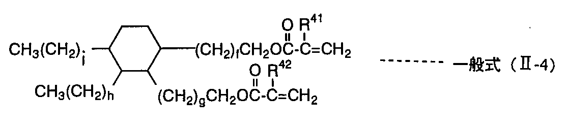
で表わされる化合物、一般式(II−4)
【0027】
【化23】
(式中、R41及びR42は水素原子又はメチル基を表わし、f、g、h及びiは各々独立的に0〜10の整数を表わす。)
で表わされる化合物及び一般式(II−5)
【0029】
【化24】
(式中、R41及びR42は水素原子又はメチル基を表わし、j、k、l及びmは各々独立的に0〜10の整数を表わす。)
で表わされる化合物から成る群から選ばれる高分子形成性化合物であることを特徴とする液晶デバイスを提供する。
【0031】
また、本発明は上記課題を解決するために、前記透明性固体物質が、前記アルキレンジ(メタ)アクリレート誘導体に加えて、更に単官能型(メタ)アクリレート誘導体を含有する重合性組成物を重合して成る透明性固体物質であり、又さらには該単官能型(メタ)アクリレート誘導体が、直鎖アルキル(メタ)アクリレート化合物、分岐アルキル鎖を有するアルキル(メタ)アクリレート化合物、あるいはこれら2種の化合物の混合物であることを特徴とし、更には又該アルキル(メタ)アクリレート化合物の炭素原子数が16〜30であることを特徴とする液晶デバイスを提供する。
【0032】
また、本発明は上記課題を解決するために、前記液晶材料が、6成分以上の化合物を含有し、複屈折率Δnが0.200以上であり、誘電率異方性Δεが5以上であり、少なくとも5〜75℃の全範囲でネマチック相を示すことを特徴とする液晶デバイスを提供する。
【0033】
更に、本発明は上記課題を解決するために、前記液晶材料が、一般式(III−1)
【0034】
【化25】
[式中、R21は炭素原子数2〜7の直鎖状アルキル基、直鎖状アルケニル基又は一般式
【0036】
【化26】
![]()
(式中、t及びuは各々独立的に1〜5の整数を表わす。)
で表わされるアルコキシアルキル基を表わし、X21はフルオロ基、クロロ基、トリフルオロメトキシ基又はトリフルオルメチル基を表わし、 Y8は水素原子又はフルオロ基を表わし、Z2は単結合、−COO−、−C2H4−、
−CH(CH3)CH2−又は−C4H8−を表わし、 環A1は1,4−シクロヘキシレン基又は1,4−フェニレン基を表わし、 sは0又は1を表わす。]
で表わされる化合物及び一般式(III−2)
【0038】
【化27】
(式中、R22は炭素原子数2〜7の直鎖状アルキル基又は直鎖状アルケニル基を表わし、X22はフルオロ基、クロロ基、トリフルオロメトキシ基又はトリフルオルメチル基を表わし、Y9は水素原子又はフルオロ基を表わし、Z3は単結合、
−COO−、−C2H4−、−CH(CH3)CH2−又は−C4H8−を表わし、環A2は1,4−シクロヘキシレン基又は1,4−フェニレン基を表わす。)
で表わされる化合物からなる第2群から選ばれる化合物を含有することを特徴とする液晶デバイスを提供する。
【0040】
更に、本発明は上記課題を解決するために、一般式(IV−1)
【0041】
【化28】
(式中、R31は炭素原子数2〜7の直鎖状アルキル基又はアルケニル基を表わし、R32は炭素原子数1〜7の直鎖状アルキル基、アルコキシ基、炭素原子数2〜5の直鎖状アルケニル基又はアルケニルオキシ基を表わし、Z4は単結合、
−COO−、−C2H4−又は−C4H8−を表わす。)
で表わされる化合物、
一般式(IV−2)
【0043】
【化29】
(式中、R33は炭素原子数2〜7の直鎖状アルキル基又はアルケニル基を表わし、R34は炭素原子数1〜7の直鎖状アルキル基、アルコキシ基、炭素原子数2〜5の直鎖状アルケニル基又はアルケニルオキシ基を表わし、Z5は単結合、
−COO−、−C2H4−又は−C4H8−を表わす。)
で表わされる化合物、
及び一般式(IV−3)
【0045】
【化30】
(式中、R35は炭素原子数2〜7の直鎖状アルキル基又はアルケニル基を表わし、R36は炭素原子数1〜7の直鎖状アルキル基、アルコキシ基、炭素原子数2〜5の直鎖状アルケニル基又はアルケニルオキシ基を表わし、Z6は単結合、
−COO−、−C2H4−又は−C4H8−を表わし、 環A3は1,4−シクロヘキシレン基又は1,4−フェニレン基を表わす。)
で表わされる化合物からなる第3群から選ばれる化合物を含有することを特徴とする液晶デバイスを提供する。
【0047】
【発明の実施の形態】
本発明の液晶デバイスは、次のようにして製造することができる。
即ち、電極層を有する少なくとも一方が透明な2枚の基板間に、(1)液晶材料、(2)高分子形成性化合物を含有する重合性組成物、(3)光重合開始剤を含有する均一溶液を介在させ、この溶液に波長350nm未満を遮断し、かつ、少なくとも波長370nm以下に光強度が存在する紫外線を照射することにより重合性組成物を重合させることによって、2枚の基板間に液晶材料を分散させた構造を有する透明性固体物質を形成して成る調光層、又は、液晶材料の連続層中に三次元網目構造を有する透明性固体物質を形成して成る調光層を形成する。
【0048】
ここで、紫外線波長350nm未満を遮断するとは、350nm未満に実質的に光強度が存在しないことを意味し、特にフィルター等を用いて紫外線の波長350nm未満を遮断することの意味は、JIS B7113(写真撮影用シャープカットガラスフィルター)により明記されているフィルターの吸収限界波長が、波長350nm以上に存在するフィルターを用いて得られた紫外線を示す。
【0049】
波長350nm未満を遮断し、かつ、少なくとも波長370nm以下に光強度が存在する紫外線を得る手段としては、例えば、紫外線カットフィルターを用いる方法や分光装置を用いる方法等が挙げられる。
【0050】
紫外線カットフィルターは、ガラスの如き堅固な材料であってもよく、プラスチックの如き柔軟性を有する材料であってもよい。又、液体状のものを容器に封入したものや透明性の板に塗布したものでもよく、粒子状に分散したものでもよい。
【0051】
紫外線をカットするフィルターとしては、例えば、「UV−37」、「SL−1A」(東芝ガラス社製)、「UV−36」、「L−37」、「L−38]、「B−480]、「LA−20」(HOYAガラス社製)等を挙げることができる。
【0052】
分光装置を用いる方法は、プリズムや回折格子等の分光光学部品を用いて、紫外線を分光し、任意の波長を有する紫外線を選択し、それらを重ね合わせて、目的のとする波長領域を有する紫外線を得る。
【0053】
本発明で使用する基板は、堅固な材料として、ガラスであっても良く、柔軟性を有する材料として、プラスチックフィルムの如きものであっても良い。この基板には、目的に応じて透明、不透明の適宜な電極が、その全面又は部分的に配置されても良い。尚、2枚の基板間には、通常、周知の液晶デバイスと同様、間隔保持用のスペーサーを介在させることもできる。本発明の液晶デバイスは、コンピュ−タ端末の表示装置やプロジェクションの表示装置等に利用される場合、透明性電極層に非線形素子又は能動素子を設けることが好ましい。
【0054】
本発明の液晶デバイスは、使用する液晶材料の液晶相の温度範囲によって液晶デバイスの動作温度範囲が制限されることから、本発明の液晶デバイスで使用する液晶材料は、広い温度で液晶相を示すものが好ましい。また、液晶デバイスのコントラストを高くする為に、本発明の液晶デバイスで使用する液晶材料は、大きな複屈折率(Δn)を示すものが好ましい。
【0055】
しかしながら、このような液晶材料には、しばしば、誘起した結晶相あるいは一部が結晶化したスメクチック相が発現し、逆に液晶相を狭くなるという問題を有したり、大きな複屈折率及び広い温度で液晶相を示すが、アクティブ・マトリクス方式に必須の特段に高い電圧保持率を達成するには至らなかった。更に、光散乱形液晶デバイスを作製した場合、電圧無印加時の光透過率T0が、 作製した直後の値あるいは電圧印加後長期に放置させた値に比べ電圧印加状態から無印加状態に切り替えた直後の値のほうが大きくなってしまうメモリー現象が発現し、結果的に液晶デバイスのコントラストを悪化させることになり、単にフルオロトラン系の液晶性化合物を含有する液晶材料を用いれば、好ましい結果に到るとは限らないものであった。
【0056】
また、液晶材料が好ましい特性を有しても、液晶デバイスを構成する透明性固体物質により、液晶デバイスのコントラストの悪化、電圧保持率の低下、あるいは不充分な電圧保持率の耐熱性等の問題を有していた。
【0057】
本発明は、液晶材料として、上記一般式(I−1)で表わされる化合物群(I−1)、上記一般式(I−2)で表わされる化合物群(I−2)及び上記一般式(I−3)で表わされる化合物群(I−3)からなる3群の化合物群のうち、2又は3群の化合物群から各々選ばれる少なくとも1つ以上の化合物を必須成分とし、かつ、透明性固体物質を形成させる重合性組成物として、上記一般式(II−1)で表わされるアルキレンジ(メタ)アクリレート誘導体より選ばれる高分子形成性化合物を必須成分とし、その中でも特に(II−2)〜(II−5)で表わされる化合物から成る群から選ばれる高分子形成性化合物を含有することによって、上記の課題を解決できることを見い出したことにある。
【0058】
上記一般式(I−1)で表わされる化合物において、X11が、フルオロ基、クロロ基、トリフルオロメトキシ基、トリフルオルメチル基の液晶性化合物は、誘電率異方性Δεが5〜25の範囲にあり、フルオロトラン構造を有するものである。上記一般式(I−1)〜(I−3)の代表的な化合物(No.1〜20)とその相転移温度を下記表1及び表2に示す。尚、下記表中、m.p.は結晶相から液晶相又は等方性液体相に相転移する温度を、c.p.は液晶相から等方性液体相に相転移する温度を夫々表わす。また、各化合物は、蒸留、カラム精製、再結晶等の方法を用いて不純物を除去し、充分精製したものを使用した。
【0059】
【表1】
【表2】
上記一般式(I−1)〜(I−3)で表わされる第1群の化合物は、シアノ基を含有していないにもかかわらず、複屈折率(Δn)が従来になく非常に大きいという特徴を有しており、これら化合物を使用することによって得られる液晶材料の複屈折率は非常に大きいものとなる。また、誘電率異方性(Δε)が大きく、電圧保持率が高いという特徴も有している。これにより、液晶デバイスの電圧無印加時の光透過率T0 や電圧保持率を向上させることができる。更に、上記一般式(I−1)〜(I−3)で表わされる第1群の化合物は、高分子形成性化合物とより高い相溶性を示す特異な現象を有している。このような効果は、表中のNo. 3〜6、9、11〜14、16〜20の化合物に有しており、多用することが好ましい。
【0062】
本発明で使用する液晶材料における各化合物の含有量は、第1群の一般式(I−1)で表わされる化合物を含有する場合、一般式(I−1)で表わされる化合物1種につき、夫々30重量%以下で含有することが好ましく、液晶材料における総含有量は、少なくとも5重量%以上の範囲が好ましく、10〜60重量%の範囲がより好ましく、15〜50重量%の範囲が特により好ましい。上記一般式(I−2)で表わされる化合物及び一般式(I−3)で表わされる化合物についても同様である。
【0063】
このような化合物を2種類以上混合することによって得た液晶材料は、広い温度範囲でネマチック液晶相を示すものであり、液晶表示装置として用いる場合、広い温度範囲で表示を可能とする。
【0064】
本発明の液晶デバイスの調光層中に占める液晶材料の比率は、60〜95重量%が好ましく、70〜90重量%の範囲が特に好ましい。
【0065】
本発明の液晶デバイスを構成する透明性固体物質は、高分子形成性化合物より成る重合組成物を重合させることにより形成することが好ましく、例えば、紫外線硬化型ビニル基を有する化合物を含有する重合性組成物及び光重合開始剤を液晶材料と混合した調光層形成材料を2枚の基板間に挟持した後、重合性組成物を光硬化させて作製する。高分子形成性化合物と液晶材料との相溶性がより高い場合、より広い温度域でより均一な溶液を得ることを可能とする。このような状態で高分子形成性化合物を硬化させると、片寄りが無いあるいは少ない状態で、光散乱性を有する調光層を作製することができ、駆動電圧やコントラスト比にムラの無い表示特性を得ると共に、白濁性のより均一な表示を達成した光散乱形液晶デバイスを提供できる。
【0066】
本発明の液晶デバイスで使用する上記一般式(II−1)〜(II−5)で表わされる高分子形成性化合物及び単官能型アルキル(メタ)アクリレートは、(メタ)アクロイルオキシ基以外の部分が、極性が低い直鎖、分岐あるいは環状の炭化水素構造より構成されるアクリレート誘導体化合物である。これらの化合物は、低極性であるため、液晶デバイスの駆動電圧を低下させる効果を有し、また、これらの化合物は、イオン性不純物との吸着性が小さいため、高抵抗であり、得られた液晶デバイスの電圧保持率を向上させることができ、更には、その耐熱性をも改善することができる。
【0067】
上記一般式(II−1)〜(II−5)で表わされる高分子形成性化合物及び単官能型アルキル(メタ)アクリレート誘導体は、上記液晶材料との相容性が高いので、均一な調光層を有する液晶デバイスを得ることができる。
【0068】
本発明で使用する上記一般式(II−1)及び(II−2)〜(II−5)で表わされる高分子形成性化合物は各々単独で使用することもできるが、混合して使用することもできる。特に、上記一般式(II−2)〜(II−5)の化合物から成る群から選ばれる高分子形成性化合物において、一般式(II−2)あるいは(II−3)の化合物は、重合性が良く上記液晶材料との相溶性も優れているため、液晶デバイスの散乱性を改善する効果が高く、又、一般式(II−4)及び(II−5)の混合物は、液晶デバイスの散乱性を向上させ、さらに液晶デバイスの駆動電圧の温度依存性を低減させるため、特に好ましい。
【0069】
本発明で使用する上記一般式(II−1)及び(II−2)〜(II−5)で表わされる代表的な高分子形成性化合物としては、例えば、1,6−ヘキサンジオールジアクリレート、1,9−ノナンジオールジアクリレート、1,12−ドデカンジオールジアクリレート、1,13−トリデカンジオールジアクリレート、1,14−テトラデカンジオールジアクリレート、3−メチル−1,5−ペンタンジオールジアクリレート、2−メチル−1,8−オクタンジオールジアクリレート、2,2−ジエチル−1,3−プロパンジオールジアクリレート、2−エチル−2−ブチルプロパンジオールジアクリレート、(1,2−ジアクロイルオキシオクチル−3−オクチル−4−ヘキシル)シクロヘキサン、9−ノニル−10−オクチルノナデカンジオールジアクリレート、オクタデカン−1,12−ジオールジアクリレート、2,4−ジエチル−1,5−オクタンジオールジアクリレート、水添ジシクロペンタジエニルジアクリレート等を挙げることができる。
【0070】
本発明で使用する上記一般式(II−1)及び(II−2)〜(II−5)で表わされる高分子形成性化合物は、例えば、(メタ)アクリル酸又は(メタ)アクリル酸クロリドを用いて、脂肪族ジオール化合物を(メタ)アクリル化することによって容易に製造することができる。
【0071】
上記一般式(II−1)及び(II−2)〜(II−5)で表わされる高分子形成性化合物の製造原料となる脂肪族ジオール化合物の市販品としては、東京化成社製の「1,6−ヘキサンジオール」、「1,9−ノナンジオール」、「1,2−テトラデカンジオール」、「ネオペンチルグリコール」、クラレ社製の「2−メチル−1,8−オクタンジオール」、「3−メチル−1,5−ペンタンジオール」、東亞合成社製の「ペスポールHP−1000((1,2−ヒドロキシオクチル−3−オクチル−4−ヘキシル)シクロヘキサンと9−ノニル−10−オクチルノナデカンジオールの混合物)」等を挙げることができる。
【0072】
本発明で使用する上記一般式(II−1)及び(II−2)〜(II−5)で表わされる高分子形成性化合物の市販品としては、例えば、共栄社化学社製の「ライトアクリレートNP−A(ネオペンチルグリコールジアクリレート)」、「ライトアクリレート1・6HX−A(1,6−ヘキサンジオールジアクリレート」、「1・9ND−A(1,9−ノナンジオールジアクリレート)」、「DCP−A」、第一製薬工業社製の「C9A(2−エチル−2−ブチルプロピレンジオールジアクリレート)」、化薬サートマー社製の「ケミリックC−2000(直鎖脂肪族ジアクリレート(C13.C14))」、新中村化学社製の「A−OCD((1,2−ヒドロキシオクチル−3−オクチル−4−ヘキシル)シクロヘキサンと9−ノニル−10−オクチルノナデカンジオールの混合物のジアクリレートエステル)」「A−ODD(主成分がオクタデカン−1,12−ジオールジアクリレート)等を挙げることができる。
【0073】
本発明で使用する上記一般式(II−1)及び(II−2)〜(II−5)で表わされる高分子形成性化合物の使用割合は、重合性組成物中の5〜95%の範囲が好ましく、20〜80%の範囲が特に好ましい。
【0074】
本発明で使用する単官能型(メタ)アクリレート誘導体は、重合硬化する際に、架橋度が低く調整されるので、液晶と高分子の界面のアンカリング力が弱まり、低電圧で駆動させる効果をもたらす。また、単官能型(メタ)アクリレート誘導体は、配合割合が大きすぎても小さすぎても高白濁性実現効果又は低電圧駆動化効果が小さくなる傾向にあるので好ましくない。このとき使用する重合性組成物中の単官能型(メタ)アクリレート誘導体の割合は、低電圧駆動を達成するために、90質量%以下の範囲が好ましく、10〜70質量%の範囲が特に好ましい。
【0075】
単官能型(メタ)アクリレート誘導体としては、(メタ)アクリル基を1つ持つ化合物であれば、いずれのものでも良いが、特に、単官能型アルキル(メタ)アクリレート誘導体は、低極性による液晶分子とのアンカーリング力低下により、更に低電圧駆動化するため、好ましい。
【0076】
アルキル(メタ)アクリレート誘導体のアルキル基の直鎖の炭素原子数は5〜23の範囲が好ましく、8〜18の範囲がより好ましい。これより炭素原子数が少ない場合は低電圧駆動化の効果が小さく、また、多すぎる場合は電圧無印加時の白濁性が低下する。又アルキル系(メタ)アクリレート誘導体は抵抗値が高く、アクティブ駆動用に好適である。
【0077】
更に、分岐鎖を有するアルキル(メタ)アクリレート類、分岐鎖を有するアルキル基置換ポリアルキレングリコール(メタ)アクリレート類、脂環式誘導(メタ)アクリレートは低温に於けるメモリー現象を防止する効果があり、汎用デバイスやアクティブ駆動用デバイスに好適である。
【0078】
更に本発明で使用する、単官能型アルキル(メタ)アクリレート誘導体のアルキル基の炭素原子数が16〜30である事が好ましい。アルキル基の炭素原子数が16未満では、パネル製造工程の真空注入時の真空度が高い場合、揮散していき易くなるため、特性的に安定したパネルが製造し難く、又調光層形成材料の繰り返し使用回数が制約されるため好ましくない。又該炭素原子数が30以上では液晶との相溶性が悪くなるため充分な散乱性を得ることが難しくなる。
【0079】
そのような単官能型アルキル(メタ)アクリレート誘導体としては、例えば、エチル(メタ)アクリレート、プロピル(メタ)アクリレート、ブチル(メタ)アクリレート、アミル(メタ)アクリレート、ヘキシル(メタ)アクリレート、ヘプチル(メタ)アクリレート、オクチル(メタ)アクリレート、ノニル(メタ)アクリレート、デシル(メタ)アクリレート、ドデシル(メタ)アクリレート、トリデシル(メタ)アクリレート、オクタデシル(メタ)アクリレート、ビフェニル(メタ)アクリレート、イソミリスチル(メタ)アクリレート、イソバルミチル(メタ)アクリレート、イソステアリル(メタ)アクリレート、イソイコシ
ル(メタ)アクリレート、イソドコシル(メタ)アクリレート、イソテトラコシル(メタ)アクリレート、イソヘキサコシル(メタ)アクリレート、イソオクタコシル(メタ)アクリレート、トリアコンチル(メタ)アクリレート、ネニル(メタ)アクリレート、ネロリジル(メタ)アクリレート、ファルネジル(メタ)アクリレート等を挙げることが出来る。
【0080】
又その他の単官能型(メタ)アクリレート誘導体としては、例えば、メトキシポリエチレングリコール(メタ)アクリレート、メトキシジエチレングリコール(メタ)アクリレート、2−メトキシエチル(メタ)アクリレート、エトキシエトキシエチル(メタ)アクリレート、ブトキシエチル(メタ)アクリレート、エトキシジエチレングリコール(メタ)アクリレート、メトキシトリエチレングリコール(メタ)アクリレート)、シクロヘキサン(メタ)アクリレート、シクロペンタン(メタ)アクリレート、シクロヘプタン(メタ)アクリレート、ビシクロヘプタン(メタ)アクリレート、ノルボルネン(メタ)アクリレート、ビシクロペンタン(メタ)アクリレート、ビシクロオクタン(メタ)アクリレート、トリシクロヘプタン(メタ)アクリレート、トリシクロデカン(メタ)アクリレート、コレステロール(メタ)アクリレート、スチレン、クロロスチレン、α−メチルスチレン、ジビニルベンゼン:置換基として、ベンジル、フェノキシエチル、アルコキシフェニル、アルリル、メタリル、グリシジル、2−ヒドロキシエチル、2−ヒドロキシプロピル、3−クロロ−2−ヒドロキシプロピル、ジメチルアミノエチル、ジエチルアミノエチル等の如き基を有するアクリレート、メタクリレート及びフマレート;1,3−ブチレングリコール、テトラメチレングリコール、ヘキサメチレングリコール、ネオペンチルグリコール、トリメチロールプロパン、グリセリン及びペンタエリスリトール等のモノ(メタ)アクリレート;酢酸ビニル、酪酸ビニル又は安息香酸ビニル、アクリロニトリル、セチルビニルエーテル、リモネン、シクロヘキセン、ジアリルフタレート、ジアリルイソフタレート、2−、3− 又は4−ビニルピリジン、アクリル酸、メタクリル酸、アクリルアミド、メタクリルアミド、N−ヒドロキシメチルアクリルアミド又はN−ヒドロキシエチルメタクリルアミド及びそれらのアルキルエーテル化合物等を挙げることができる。
【0081】
本発明においては、重合性組成物として、上記以外の各種多官能(メタ)アクリレート誘導体を併用することができる。
そのような多官能(メタ)アクリレート誘導体としては、例えば、1,3−ブチレングリコール、テトラメチレングリコール、ヘキサメチレングリコール、ネオペンチルグリコール、トリメチロールプロパン、グリセリン及びペンタエリスリトール等のポリ(メタ)アクリレート;ネオペンチルグリコール1モルに2モル以上のエチレンオキサイド若しくはプロピレンオキサイドを付加して得たジオールのジ(メタ)アクリレート;トリメチロールプロパン1モルに3モル以上のエチレンオキサイド若しくはプロピレンオキサイドを付加して得たトリオールのジ又はトリ(メタ)アクリレート;ビスフェノールA1モルに2モル以上のエチレンオキサイド若しくはプロピレンオキサイドを付加して得たジオールのジ(メタ)アクリレート;2−ヒドロキシエチル(メタ)アクリレート1モルとフェニルイソシアネート若しくはn−ブチルイソシアネート1モルとの反応生成物;ジペンタエリスリトールのポリ(メタ)アクリレート;トリメチロールプロパントリアクリレート、トリシクロデカンジメチロールジアクリレート、トリス−(アクリルオキシエチル)イソシアヌレート、カプロラクトン変性ヒドロキシピバリン酸エステルネオペンチルグリコールジアクリレートを挙げることができる。
【0082】
光重合開始剤としては、例えば、2−ヒドロキシ−2−メチル−1−フェニルプロパン−1−オン(メルク社製「ダロキュア1173」)、1−ヒドロキシシクロヘキシルフェニルケトン(チバ・ガイギー社製「イルガキュア184」)、1−(4−イソプロピルフェニル)−2−ヒドロキシ−2−メチルプロパン−1−オン(メルク社製「ダロキュア1116」)、ベンジルジメチルケタール(チバ・ガイギー社製「イルガキュア651」)、2−メチル−1−〔4−(メチルチオ)フェニル〕−2−モルホリノプロパノン−1(チバ・ガイギー社製「イルガキュア907」)、2,4−ジエチルチオキサントン(日本化薬社製「カヤキュアDETX」)とp−ジメチルアミノ安息香酸エチル(日本化薬社製「カヤキュアEPA」)との混合物、イソプロピルチオキサントン(ワードプレキンソツプ社製「カンタキュアーITX」)とp−ジメチルアミノ安息香酸エチルとの混合物、アシルホスフィンオキシド(BASF社製「ルシリンTPO」)等が挙げられ、特に、2−ヒドロキシ−2−メチル−1−フェニルプロパン−1−オン(メルク社製「ダロキュア1173」)、1−ヒドロキシシクロヘキシルフェニルケトン(チバ・ガイギー社製「イルガキュア184」)、ベンジルジメチルケタール(チバ・ガイギー社製「イルガキュア651」)が好ましい。
【0083】
調光層形成材料中の光重合開始剤の使用割合は、0.05〜2.5重量%の範囲が好ましく、0.1〜1.0%の範囲が特に好ましい。光重合開始剤が0.05重量%より少ない場合、調光層形成時の重合組成物の重合速度が遅くなり、適切な網目構造が形成できず、光散乱が低下する傾向があるので、好ましくなく、2.5重量%より多い場合、液晶デバイスの電圧保持率が低下する傾向があるので、好ましくない。
【0084】
本願請求項9記載の発明において使用する6成分以上の液晶性化合物を含有し、複屈折率(△n)が0.200以上であって、誘電率異方性△εが5以上であり、少なくとも5〜75℃でネマチック相を示す液晶材料は、アクティブ・マトリックス方式において必要な高い電圧保持率を得るために、有用である。そのような液晶材料は、上記一般式(I−1)で表わされる化合物群(I−1)、上記一般式(I−2)で表わされる化合物群(I−2)及び上記一般式(I−3)で表わされる化合物群(I−3)からなる3群の化合物群のうち、2又は3群の化合物群から各々選ばれる少なくとも1つ以上の化合物を必須成分とし、かつ、第3成分を含有する場合、シアノ基を有しない液晶性化合物を用いることが好ましい。使用する液晶性化合物としては、トラン系化合物が好ましく、フルオロトラン系化合物が特に好ましく、少なくとも1種以上の3つの環を有するフルオロトラン系化合物を主構成成分として使用することがより好ましい。
【0085】
使用する液晶材料の誘電率異方性△εは、5〜20の範囲が好ましい。フルオロトラン系化合物は、誘電率異方性(Δε)が5以上であり、低い駆動電圧特性を得るのに好ましい。
【0086】
このような化合物を少なくとも6成分以上の化合物で混合することによって、より好ましくは7〜20成分で構成することによって、得られる液晶材料は、広い温度範囲でネマチック相を示すことができ、液晶表示装置として用いる場合、より広い温度範囲で表示を可能とする。
【0087】
高い電圧保持率を有する液晶デバイスを調製するには、より高い比抵抗の液晶材料を用いることが好ましく、比抵抗としては1011Ω・cm以上が好ましく、1012Ω・cm以上がより好ましく、1013Ω・cm以上が最も好ましい。
【0088】
本願請求項10に記載の発明は、上記一般式(I−1)で表わされる化合物群(I−1)、上記一般式(I−2)で表わされる化合物群(I−2)及び上記一般式(I−3)で表わされる化合物群(I−3)からなる3群の化合物群のうち、2又は3群の化合物群から各々選ばれる少なくとも1つ以上の化合物を必須成分として含有し、これと組み合わせて用いる化合物として、上記一般式(III−1)で表わされる化合物及び上記一般式(III−2) で表わされる化合物から成る第2群から選ばれる化合物を見い出し、この液晶材料を用いた液晶デバイスは、この液晶材料の液晶相より広い温度域で、特に、低温での動作が可能な特性を示すことを見い出したことに特徴を有する。
【0089】
更に本願請求項11の発明は、上記一般式(I−1)で表わされる化合物群(I−1)、上記一般式(I−2)で表わされる化合物群(I−2)及び上記一般式(I−3)で表わされる化合物群(I−3)からなる3群の化合物群のうち、2又は3群の化合物群から各々選ばれる少なくとも1つ以上の化合物を必須成分として含有し、必要に応じて、上記一般式(III−1)で表わされる化合物及び上記一般式(III−2) で表わされる化合物から成る第2群から選ばれる化合物を含有する液晶材料に、上記一般式(IV−1)〜(IV−3)で表わされる化合物を含有させることによって、上述した高い相溶性を損なうことがないか、あるいは改善されることを見い出したことに特徴を有する。
【0090】
上記一般式(III−1)〜(III−2)で表わされる第2群の化合物及び上記一般式(IV−1)〜(IV−3)で表わされる第3群の化合物は、誘電率異方性、弾性定数あるいは粘性を調整するのに有用であり、液晶デバイスの特性を改善させることが可能なものである。
【0091】
上記一般式(III−1)〜(III−2)で表わされる第2群の化合物及び一般式(IV−1)〜(IV−3)で表わされる第3群の化合物の具体例を下記表3に示した。
【0092】
【表3】
上記一般式(I−1)で表わされる化合物群(I−1)、上記一般式(I−2)で表わされる化合物群(I−2)及び上記一般式(I−3)で表わされる化合物群(I−3)からなる3群の化合物群のうち、2又は3群の化合物群から各々選ばれる少なくとも1つ以上の化合物を必須成分として含有する液晶材料に、第2群から選ばれる化合物及び/又は第3群から選ばれる化合物を加えることによって、液晶材料の複屈折率(Δn)を用途に応じて容易に最適化することができる。第2群から選ばれる化合物及び第3群から選ばれる化合物は、必須成分としてが入する液晶性化合物との相溶性が良好であり、結晶相又はスメクチック相とネマチック相との相転移温度を低温側に拡大し易い傾向を示す。特に、上記一般式(III−1)で表わされる化合物は、 この効果が大きい。更に、上記一般式(IV−1)又は上記一般式(IV−4)で表わされる化合物は、液晶材料の粘性を低減させる効果も同時に示すので、優れている。
【0094】
本発明で使用する液晶材料における各化合物の含有量は、第2群の一般式(III−1) で表わされる化合物1種につき、夫々0〜20重量%の範囲で含有することが好ましく、液晶材料中における総含有量は、多くとも50重量%以下の範囲が好ましく、0〜40重量%の範囲がより好ましく、5〜30重量%の範囲が特により好ましい。一般式(III−2)で表わされる化合物についても同様である。
【0095】
本発明で使用する液晶材料における各化合物の含有量は、第3群の一般式(IV−1)で表わされる化合物1種につき、夫々0〜30重量%の範囲で含有することが好ましく、液晶材料中における総含有量は、多くとも40重量%以下の範囲が好ましく、0〜30重量%の範囲がより好ましく、5〜20重量%の範囲が特に好ましい。一般式(IV−2)〜(IV−3)で表わされる化合物についても同様である。
【0096】
第2群、第3群の化合物において、R21、R22、R31〜R36がアルケニル基である化合物を組み合わせると、液晶相、白濁性、駆動電圧を更に改善させる効果が期待され、特に末端基がCH2=CH−(CH2)−のアルケニル基である場合、弾性定数の調整に優位である。
【0097】
一般式(III−1)で表わされる化合物及び一般式(III−2)で表わされる化合物において、環A1及びA2が、1,4−フェニレン基である化合物が好ましい。
【0098】
本願請求項12記載の発明は、液晶材料として、一般式(I−2)で表わされる化合物及び一般式(I−3)で表わされる化合物から成る群から選ばれた1種又はそれ以上の化合物において、1個又はそれ以上の水素原子を重水素原子に置換したシクロヘキサン環を1個又は2個有する化合物を用いる点に特徴を有する。このようにして得た液晶材料は、低温でのネマチック相を安定化させたり、低温保存に対しネマチック液晶性をより長期に保持できるものである。本発明者らは、重水素原子に置換したシクロヘキサン環を有する化合物を用いたこのような効果を特開平6−312949号公報、特開平7−34066号公報等で明らかにした。また、液晶デバイスの表示特性においても、重水素原子に置換したシクロヘキサン環を有した化合物が、重水素原子に置換されていないシクロヘキサン環を有した化合物と比較して、有為差のある弾性定数又はそれらの比を示しており、この弾性定数の関係を後述するような方法に応用することによって、駆動電圧等の電気光学特性を調整できるものである。
【0099】
本発明者らは、特開平6−222320号公報において、液晶材料の物性値と液晶デバイスの表示特性との関係が次式(a)で表わされることを示した。
【0100】
【数1】
なお、Vthはしきい値電圧を表わし、1Kii及び2Kiiは弾性定数を表わし、iは1、2又は3を表わし、△εは誘電率異方性を表わし、<r>は透明性固体物質界面の平均空隙間隔を表わし、Aは液晶分子に対する透明性固体物質のアンカリングエネルギーを表わし、dは透明性電極を有する基板間の距離を表わす。
【0102】
この数式は、透明性固体界面が液晶分子に与える規制力が弾性定数KiiとアンカリングエネルギーAの比によって変化することを意味しており、特にその効果が実際の平均空隙間隔<r>よりKii/Aの量だけ実質的に広げる作用を為し、従って、効果的に駆動電圧を低減させることを示している。この関係は、本発明においても応用することができ、液晶材料を構成する液晶性化合物によって液晶材料の誘電率異方性Δεと弾性定数を選定することにより、低い電圧で駆動するより好ましい液晶デバイスを得ることができる。
【0103】
高い温度域での動作特性を重視する場合は、上記一般式(I−1)で表わされる化合物及び上記一般式(I−2)で表わされる化合物と、上記一般式(III−2)で表わされる化合物、 上記一般式(IV−3)とを組み合わせた液晶材料を用いることが好ましい。低い温度域での動作特性を重視する場合は、上記一般式(I−2)及び(I−3)で表わされる化合物、 上記一般式(III−1)で表わされる化合物、上記一般式(IV−1)〜(IV−3)で表わされる化合物とを組み合わせることが好ましい。
【0104】
高い白濁性を得る目的には、上記一般式(I−1)〜(I−3)で表わされる化合物で組み合わせることが好ましく、 更に上記一般式(III−2)で表わされる化合物と組み合わせることが好ましい。
【0105】
低駆動電圧を得る目的には、上記一般式(I−1)及び(I−2)で表わされる化合物と、 上記一般式(III−1)で表わされる化合物とを組み合わせることが好ましい。
【0106】
本発明で使用する液晶材料は、上記に示した化合物の他、液晶材料の他の特性、即ち等方性液体と液晶の相転移温度、融点、粘度、Δn、重合性組成物等との溶解性及び透明性固体物質界面の改質等を改善することを目的として、適宜通常この技術分野で液晶材料として認識されるものを混合しても良いが、シアノ基を有する液晶性化合物を含有する液晶材料は、電圧保持率を低下させる傾向にあるため、分子内にシアノ基を有しない液晶性化合物が第三成分の液晶材料として好ましい、そのような液晶材料としては、例えば、アルキル基、アルケニル基、アルコキシル基、フルオロ基、クロロ基、トリフルオロメチル基、トリフルオロメトキシ基を置換基として有する4−置換安息香酸4−置換フェニルエステル、4−置換シクロヘキサンカルボン酸4−置換フェニルエステル、4−置換シクロヘキサンカルボン酸4’−置換ビフェニルエステル、(4−置換シクロヘキサンカルボニルオキシ)安息香酸4−フェニルエステル、(4−置換シクロヘキシル)安息香酸4−置換シクロヘキサンエステル、4−置換4’−置換ビフェニル、4−置換4”−置換ターフェニル等の液晶性化合物が挙げられる。
【0107】
本発明で使用する液晶材料は、透明性電極層を有する2枚の基板間に液晶材料の小滴を透明性固体物質中に分散させたデバイスにも有用なものであることが期待される。基板間に形成される透明性固体物質は、繊維状あるいは粒子状に分散するものでも、液晶材料を小滴状に分散させたフィルムのものでも良いが、三次元網目状の構造を有するものがより好ましい。
【0108】
このような透明性固体物質から形成された三次元網目状構造の網目サイズは、光の波長に比べて大きすぎたり、小さすぎる場合、光散乱性が衰える傾向にあるので、0.5〜3μmの範囲が好ましい。また、調光層の厚みは、使用目的に応じ、2〜50μmの範囲が好ましく、5〜30μmの範囲が特に好ましい。
【0109】
このようにして製造された本発明の液晶デバイスは、本発明者らが光散乱不透明状態と透明状態を利用する液晶デバイスを構成する液晶材料と透明性固体物質について鋭意検討し、液晶材料を構成する液晶性化合物、高分子形成性化合物との相溶性及び重合性組成物の好ましい構成を見い出したことにより、より低い電圧駆動性やより高い調光層の抵抗値、あるいはより高いコントラスト比等の表示特性を維持向上させると共に、メモリー現象を低減し、白濁性のより均一な表示を達成し、これにより、アクティブ・マトリクス方式に要求される特性を有するものである。また、本発明の液晶デバイスは、例えば、プロジェクション表示装置として利用することができる。
【0110】
【実施例】
以下、実施例を用いて本発明を更に詳細に説明する。しかしながら、本発明はこれらの実施例に限定されるものではない。
【0111】
なお、以下の実施例及び比較例において「%」は「重量%」を表わす。また、各実施例及び比較例中の評価特性の各々は以下の記号及び内容を意味する。
【0112】
(1)V90、V10:
電圧無印加時のデバイスの光透過率(T0)を0%とし、 印加電圧の増大に伴って光透過率が変化しなくなったときの透過率(T100) を100%とする時、光透過率90%と成る印加電圧(V)をV90、光透過率10%と成るときの印加電圧をV10とする。
【0113】
(2)コントラスト:
デバイスを測光上から外した状態で、光源の点灯時の光透過率を100%とし、消灯時の光透過率を0%とし、電圧無印加時のデバイスの光透過率をT0、 印加電圧の増大に伴って飽和した光透過率をT100とするとき、 T100/T0で表わされる値である。尚、集光角が6゜となる光学装置を用いて測定した。
【0114】
(3)保持率:
デバイスを150℃の温度で1時間エージングした後、温度80℃、フレーム周波数60Hz、ピーク電圧V90、ON状態の時間64μ秒の矩形波を印加し、ON状態で蓄積された電荷をQ0、 OFF状態で漏れる電流を高インピーダンス電圧計で測定し、残存電荷をQとしたとき、 (Q/Q0)×100で表わされる値である。
【0115】
(4)TMLC:
液晶材料と高分子形成性化合物を均一溶液となるに必要な温度で混合した混合物において、冷却時に等方性液体からネマチック相に転移温度又は相分離する温度とする。
【0116】
なお、 各液晶材料の物性として記載されたTN-Iはネマチック相−等方性液体相転移温度を、△εは誘電異方性を、△nは複屈折率を意味しており、Vthは8μmのTN型液晶デバイスで測定されたしきい値電圧を示したものである。
【0117】
【0118】
液晶組成物(3−1)の組成:
【0119】
【化31】
この調光層形成材料を、平均粒径10μmのスペーサーが介在した2枚のITO電極ガラス基板を用いて作製した大きさ50×50mmの空セルに、均一溶液の転移温度TMLCより10℃高い温度の下で真空注入した。 これを、均一溶液の転移温度TMLCより3℃高い温度に保持しながら、 「UV−36」(HOYAガラス社製、360nm付近以下をカット)を介して、 15mW/cm2の照度のメタルハライドランプ紫外線を60秒照射して高分子形成化合物を硬化させて、液晶材料と透明性固体物質から成る調光層を有する液晶デバイスを得た。得られた液晶デバイスについて、基板間に形成された硬化物の断面を走査型電子顕微鏡を用いて観察したところ、ポリマーから成る三次元ネットワーク構造の透明性固体物質が認められた。得られた液晶デバイスは、ムラの無い均一な表示特性を示しており、その諸特性は、以下の通りであった。
【0122】
液晶デバイスの特性:
V10 : 4.8 V
V90 : 7.5 V
T0 : 1.80%
T100 : 88.1 %
コントラスト: 1:49
保持率 : 98.8 %
【0123】
実施例1で得た液晶デバイスは、均一でむらのない表示特性を達成し、かつ、低電圧で駆動し、高電圧保持率を有する信頼性の高いものであった。
【0124】
(実施例2)
実施例1において、液晶組成物(3−1)に代えて、下記液晶組成物(3−2)を使用した以外は、実施例1と同様にして液晶材料と透明性固体物質から成る調光層を有する液晶デバイスを得た。得られた液晶デバイスの諸特性は以下の通りであった。
【0125】
液晶組成物(3−2)の組成:
【0126】
【化32】
液晶デバイスの特性:
V10 : 4.5 V
V90 : 6.8 V
T0 : 1.60%
T100 : 88.6 %
コントラスト: 1:55
保持率 : 98.6 %
【0129】
実施例2で得た液晶デバイスは、均一でむらのない表示特性を達成し、かつ、低電圧で駆動し、高電圧保持率を有する信頼性の高いものであった。
【0130】
(実施例3)
実施例1において、液晶組成物(3−1)に代えて、下記液晶組成物(3−3)を使用した以外は、実施例1と同様にして液晶材料と透明性固体物質から成る調光層を有する液晶デバイスを得た。得られた液晶デバイスの諸特性は以下の通りであった。
【0131】
液晶組成物(3−3)の組成:
【0132】
【化33】
液晶デバイスの特性:
V10 : 3.3 V
V90 : 5.0 V
T0 : 0.80%
T100 : 88.4 %
コントラスト: 1:111
保持率 : 98.8 %
【0135】
実施例3で得た液晶デバイスは、均一でむらのない表示特性を達成し、かつ、低電圧で駆動し、高電圧保持率を有する信頼性の高いものであった。
【0136】
(実施例4)
実施例1において、液晶組成物(3−1)に代えて、下記液晶組成物(3−4)を使用した以外は、実施例1と同様にして液晶材料と透明性固体物質から成る調光層を有する液晶デバイスを得た。得られた液晶デバイスの諸特性は以下の通りであった。
【0137】
液晶組成物(3−4)の組成:
【0138】
【化34】
液晶デバイスの特性:
V10 : 4.6 V
V90 : 6.5 V
T0 : 1.15%
T100 : 87.9 %
コントラスト: 1:76
保持率 : 98.5 %
【0141】
実施例4で得た液晶デバイスは、均一でむらのない表示特性を達成し、かつ、低電圧で駆動し、高電圧保持率を有する信頼性の高いものであった。
【0142】
(実施例5)
実施例1において、液晶組成物(3−1)に代えて、下記液晶組成物(3−5)を使用した以外は、実施例1と同様にして液晶材料と透明性固体物質から成る調光層を有する液晶デバイスを得た。得られた液晶デバイスの諸特性は以下の通りであった。
【0143】
液晶組成物(3−5)の組成:
【0144】
【化35】
液晶デバイスの特性:
V10 : 3.2 V
V90 : 8.2 V
T0 : 1.50%
T100 : 87.6 %
コントラスト: 1:58
保持率 : 98.7 %
【0147】
実施例5で得た液晶デバイスは、均一でむらのない表示特性を達成し、かつ、低電圧で駆動し、高電圧保持率を有する信頼性の高いものであった。
【0148】
(実施例6)
実施例1において、液晶組成物(3−1)に代えて、下記液晶組成物(3−6)を使用した以外は、実施例1と同様にして液晶材料及び透明性固体物質から成る調光層を有する液晶デバイスを得た。得られた液晶デバイスの諸特性は、以下の通りであった。
【0149】
液晶組成物(3−6)の組成:
【0150】
【化36】
液晶デバイスの特性:
V10 : 3.4 V
V90 : 8.5 V
T0 : 1.80%
T100 : 88.7 %
コントラスト: 1:49
保持率 : 96.3 %
【0153】
上記液晶組成物(3−5)の結晶相−ネマチック相転移温度(TCN)は2℃であったが、実施例6で得た液晶デバイスは、−15〜2℃の温度範囲でも動作可能であった。このような特性は、従来の光散乱形液晶デバイスと比較して、広い動作温度範囲を示し、かつ均一でむらのない表示特性を達成し、広告板等の装飾表示板や時計等の表示装置、又はプロジェクション表示装置等に有用なものであった。
【0154】
(比較例1)
実施例1において、液晶組成物(3−1)に代えて、下記液晶組成物(3−7)を使用した以外は、実施例1と同様にして液晶材料と透明性固体物質から成る調光層を有する液晶デバイスを得た。得られた液晶デバイスの諸特性は以下の通りであった。
【0155】
液晶組成物(3−7)の組成:
【0156】
【化37】
液晶デバイスの特性:
V10 : 3.2 V
V90 : 8.2 V
T0 : 2.80%
T100 : 88.8 %
コントラスト: 1:32
保持率 : 10.1%
【0159】
比較例1で得た液晶デバイスは、広い動作温度範囲を示し、かつ均一でむらのない表示特性を達成しているが、液晶材料がシアノ基を有する液晶性化合物を含有するため、高温エージング後の電圧保持率が大きく低下し、アクティブ・マトリクス方式駆動ができないことが理解できる。
【0160】
(実施例7)
実施例1において、高分子形成性化合物「A−OCD」に代えて、「ケミリックC−2000」(化薬サートマー社製、炭素原子数14〜15の直鎖脂肪族ジアクリレート)を使用した以外は、実施例1と同様にして液晶材料と透明性固体物質から成る調光層を有する液晶デバイスを得た。得られた液晶デバイスの諸特性は以下の通りであった。
【0161】
液晶デバイスの特性:
V10 : 4.8 V
V90 : 7.1 V
T0 : 1.80%
T100 : 87.1 %
コントラスト: 1:48
保持率 : 98.3%
【0162】
実施例7で得た液晶デバイスは、均一でむらのない表示特性を達成し、かつ、低電圧で駆動し、高電圧保持率を有する信頼性の高いものであった。
【0163】
(実施例8)
実施例1において、高分子形成性化合物「A−OCD」に代えて、「C9A」(第一製薬工業社製、2−エチル−2−ブチルプロピレンジオールジアクリレート)を使用した以外は、実施例1と同様にして液晶材料と透明性固体物質から成る調光層を有する液晶デバイスを得た。得られた液晶デバイスの諸特性は以下の通りであった。
【0164】
液晶デバイスの特性:
V10 : 5.0 V
V90 : 7.8 V
T0 : 1.85%
T100 : 88.9 %
コントラスト: 1:48
保持率 : 98.8%
【0165】
実施例8で得た液晶デバイスは、均一でむらのない表示特性を達成し、かつ、低電圧で駆動し、高電圧保持率を有する信頼性の高いものであった。
【0166】
(実施例9)
実施例1において、高分子形成性化合物「L−A」に代えて、「IM−A」(共栄社化学社製、イソミリスチルアクリレート)を使用した以外は、実施例1と同様にして液晶材料と透明性固体物質から成る調光層を有する液晶デバイスを得た。得られた液晶デバイスの諸特性は以下の通りであった。
【0167】
液晶デバイスの特性:
V10 : 5.2 V
V90 : 7.9 V
T0 : 1.81%
T100 : 89.0 %
コントラスト: 1:49
保持率 : 98.5%
【0168】
実施例9で得た液晶デバイスは、均一でむらのない表示特性を達成し、かつ、低電圧で駆動し、高電圧保持率を有する信頼性の高いものであった。
【0169】
(実施例10)
実施例1において、高分子形成性化合物「L−A」に代えて、「LTA」(大阪有機化学社製、ドデシルアクリレート、イソドデシルアクリレート、トリデシルアクリレート、イソトリデシルアクリレートの混合物)を使用した以外は、実施例1と同様にして液晶材料と透明性固体物質から成る調光層を有する液晶デバイスを得た。得られた液晶デバイスの諸特性は以下の通りであった。
【0170】
液晶デバイスの特性:
V10 : 4.9 V
V90 : 7.1 V
T0 : 1.8%
T100 : 89.5 %
コントラスト: 1:50
保持率 : 98.4%
【0171】
実施例10で得た液晶デバイスは、均一でむらのない表示特性を達成し、かつ、低電圧で駆動し、高電圧保持率を有する信頼性の高いものであった。
【0172】
【0173】
液晶デバイスの特性:
V10 : 3.2 V
V90 : 4.9 V
T0 : 1.8%
T100 : 89.5 %
コントラスト: 1:50
保持率 : 98.5%
【0174】
実施例11で得た液晶デバイスは、均一でむらのない表示特性を達成し、かつ、低電圧で駆動し、高電圧保持率を有する信頼性の高いものであった。
【0175】
(比較例2)
実施例1において、高分子形成性化合物「A−OCD」に代えて、「A−400」(新中村化学社製、ポリエチレングリコールジアクリレート)を使用した以外は、実施例1と同様にして液晶材料と透明性固体物質から成る調光層を有する液晶デバイスを得た。得られた液晶デバイスの諸特性は以下の通りであった。
【0176】
液晶デバイスの特性:
V10 : 5.1 V
V90 : 9.6 V
T0 : 1.80%
T100 : 88.6%
コントラスト: 1:49
保持率 : 25.3%
【0177】
比較例2で得た液晶デバイスは、高分子形成性化合物として、極性基を有するモノマー材料を含有するため、高温エージング後の電圧保持率が大きく低下し、アクティブ・マトリクス方式駆動ができないことが理解できる。
【0178】
(比較例3)
実施例1において、高分子形成性化合物「A−OCD」に代えて、「R−551」(日本化薬社製、エチレンオキシド変性ビスフェノールAジアクリレート)を使用した以外は、実施例1と同様にして液晶材料と透明性固体物質から成る調光層を有する液晶デバイスを得た。得られた液晶デバイスの諸特性は以下の通りであった。
【0179】
液晶デバイスの特性:
V10 : 9.5 V
V90 : 15.1 V
T0 : 1.80%
T100 : 84.3 %
コントラスト: 1:47
保持率 : 40.3%
【0180】
比較例3で得た液晶デバイスは、高分子形成性化合物として、極性基を有するモノマー材料を含有するため、高温エージング後の電圧保持率が大きく低下し、アクティブ・マトリクス方式駆動ができないことが理解できる。
【0181】
(比較例4)
実施例1の調光層形成材料を、平均粒径10μmのスペーサーが介在した2枚のITO電極ガラス基板を用いて作製した大きさ50×50mmの空セルに、均一溶液の転移温度TMLCより10℃高い温度の下で真空注入した。 これを、均一溶液の転移温度TMLCより3℃高い温度に保持しながら、 「UV−34」(HOYAガラス社製、340nm付近以下をカット)を介して、 15mW/cm2の照度のメタルハライドランプ紫外線を60秒照射して高分子形成化合物を硬化させて、液晶材料と透明性固体物質から成る調光層を有する液晶デバイスを得た。得られた液晶デバイスについて、基板間に形成された硬化物の断面を走査型電子顕微鏡を用いて観察したところ、三次元ネットワーク構造の透明性固体物質は認められなかった。得られた液晶デバイスの諸特性は、以下の通りであった。
【0182】
液晶デバイスの特性:
V10 : 4.5 V
V90 : 7.1 V
T0 : 1.9%
T100 : 89.0 %
コントラスト: 1:47
保持率 : 75.6 %
【0183】
比較例4で得た液晶デバイスは、340nm付近以下の紫外線をカットしたため、電圧保持率がやや低下し、アクティブ・マトリクス方式駆動は可能ではあるものの、十分な信頼性が得られていないことが理解できる。
【0184】
(実施例12)
実施例1において、高分子形成性化合物「ラウリルアクリレート」に代えて、「NKエステルISA」(新中村化学社製、イソステアリルアクリレート)を使用した以外は、実施例1と同様にして液晶材料と透明性固体物質から成る調光層を有する液晶デバイスを得た。得られた液晶デバイスの諸特性は以下の通りであった。
【0185】
液晶デバイスの特性:
V10 : 3.8 V
V90 : 6.1 V
T0 : 2.0 %
T100 : 88.5 %
コントラスト: 1:45
保持率 : 97.8%
【0186】
実施例12で得た液晶デバイスは、均一でむらのない表示特性を達成し、かつ、低電圧で駆動し、高電圧保持率を有する信頼性の高いものであった。
又、回収された調光層形成材料の繰り返し使用可能回数は約50回と実施例1の5回に比べ飛躍的に多いものであった。
【0187】
【0188】
液晶デバイスの特性:
V10 : 3.5 V
V90 : 5.5 V
T0 : 2.2%
T100 : 89.4 %
コントラスト: 1:41
保持率 : 98.5%
【0189】
実施例13で得た液晶デバイスは、均一でむらのない表示特性を達成し、かつ、低電圧で駆動し、高電圧保持率を有する信頼性の高いものであった。
又、回収された調光層形成材料の繰り返し使用可能回数は約60回と実施例11の10回に比べ多いものであった。
【0190】
(実施例14)
実施例13において、高分子形成性化合物「NKエステルISA」に代えて、「NKエステルISA」6.8%、「TO−1336」(東亞合成社製、イソセチルアクリレート)4.0%の混合物を使用した以外は、実施例1と同様にして液晶材料と透明性固体物質から成る調光層を有する液晶デバイスを得た。得られた液晶デバイスの諸特性は以下の通りであった。
【0191】
液晶デバイスの特性:
V10 : 3.8 V
V90 : 6.0 V
T0 : 2.5 %
T100 : 89.4 %
コントラスト: 1:36
保持率 : 97.8%
【0192】
実施例14で得た液晶デバイスは、均一でむらのない表示特性を達成し、かつ、低電圧で駆動し、高電圧保持率を有する信頼性の高いものであった。
又、回収された調光層形成材料の繰り返し使用可能回数は約40回と実施例1の5回に比べ飛躍的に多いものであった。
【0193】
(実施例15)
実施例13において、高分子形成性化合物「NKエステルISA」に代えて、「TO−1339」(東亞合成社製、イソテトラコサニルアクリレート)(6.8%、「ライトエステルIS−A」(共栄社製、イソステアリルアクリレート)4.0%の混合物を使用した以外は、実施例1と同様にして液晶材料と透明性固体物質から成る調光層を有する液晶デバイスを得た。得られた液晶デバイスの諸特性は以下の通りであった。
【0194】
液晶デバイスの特性:
V10 : 3.4 V
V90 : 5.7 V
T0 : 2.8 %
T100 : 89.5 %
コントラスト: 1:32
保持率 : 98.8%
【0195】
実施例15で得た液晶デバイスは、均一でむらのない表示特性を達成し、かつ、低電圧で駆動し、高電圧保持率を有する信頼性の高いものであった。
又、回収された調光層形成材料の繰り返し使用可能回数は約60回と実施例1の5回に比べ飛躍的に多いものであった。
【0196】
(実施例16)
実施例13において、高分子形成性化合物「A−OCD」に代えて、「A−ODD」(新中村化学社製、オクタデカン−1,12−ジオールジアクリレートを使用した以外は、実施例1と同様にして液晶材料と透明性固体物質から成る調光層を有する液晶デバイスを得た。得られた液晶デバイスの諸特性は以下の通りであった。
【0197】
液晶デバイスの特性:
V10 : 4.3 V
V90 : 6.5 V
T0 : 1.7 %
T100 : 89.3 %
コントラスト: 1:53
保持率 : 97.5%
【0198】
実施例16で得た液晶デバイスは、均一でむらのない表示特性を達成し、かつ、低電圧で駆動し、高電圧保持率を有する信頼性の高いものであった。
又、回収された調光層形成材料の繰り返し使用可能回数は約50回と多いものであった。
【0199】
(実施例17)
実施例13において、高分子形成性化合物「A−OCD」に代えて、「DCP−A」(共栄化学社製、水添ジシクロペンタジエニルジアクリレート)
を使用した以外は、実施例1と同様にして液晶材料と透明性固体物質から成る調光層を有する液晶デバイスを得た。得られた液晶デバイスの諸特性は以下の通りであった。
【0200】
液晶デバイスの特性:
V10 : 4.8 V
V90 : 7.5 V
T0 : 1.6 %
T100 : 88.9 %
コントラスト: 1:56
保持率 : 98.0%
【0201】
実施例17で得た液晶デバイスは、均一でむらのない表示特性を達成し、かつ、低電圧で駆動し、高電圧保持率を有する信頼性の高いものであった。
又、回収された調光層形成材料の繰り返し使用可能回数は約50回と多いものであった。
【0202】
【発明の効果】
本発明の液晶デバイスは、より低い電圧駆動性やより高い調光層の電圧保持率、あるいはより高いコントラスト比等の表示特性が維持向上したものであり、メモリー現象が低減し、白濁性のより均一な表示を示し、アクティブ・マトリクス方式に要求される特性を有するものであるので、例えば、プロジェクション表示装置として利用することができる。また、液晶デバイスの真空注入法を用いるパネル製造工程において、調光層形成材料の使用回数を大幅に向上することが可能となるため、パネルコストを低減させることができる。[0001]
BACKGROUND OF THE INVENTION
The present invention relates to a liquid crystal device which does not use a polarizing plate and a liquid crystal device having a light control layer containing a transparent solid substance, and more specifically, a light scattering type capable of electrically or thermally controlling the blocking and transmission of a visual field. It relates to the liquid crystal device. The liquid crystal device of the present invention is used as a screen for blocking visual field in a building window, a show window, etc., displays characters and figures, and switches the display electrically or thermally with high-speed response, thereby providing an advertising board. It can be used as a decorative display board such as a clock, a display device for a calculator, a display device requiring a bright screen, particularly a display device for a computer terminal or a projection display device.
[0002]
[Prior art]
As a method for producing a bright and high-contrast liquid crystal device without requiring a polarizing plate or an alignment treatment, a method of dispersing liquid crystal droplets in a polymer and forming the polymer into a film is known. In Japanese Patent Publication No. 58-501631 and US Pat. No. 4,435,047, gelatin, gum arabic, polyvinyl alcohol and the like are proposed as encapsulating materials. This is known in Japanese Patent Laid-Open No. 62-2231.
[0003]
However, in a liquid crystal device in which liquid crystal droplets are dispersed in a polymer, 25 V or more is required to obtain sufficient transparency in addition to the trouble of optimizing the coincidence / mismatch between the individual refractive index of the liquid crystal material and the refractive index of the polymer. However, it does not have the low drive voltage characteristics that are important in the practical application of liquid crystal devices for display.
[0004]
US Pat. No. 5,304,323, Japanese Patent Application Laid-Open No. 1 (1999) discloses a technology that enables low voltage drivability, high contrast, and time-division drivability, which are important characteristics required for practical use of liquid crystal display devices. JP-A-198725 discloses a liquid crystal device having a structure in which a liquid crystal material forms a continuous layer, and polymer substances are distributed in a three-dimensional network in the continuous layer.
[0005]
As a liquid crystal material related to this purpose, for example, European Patent No. 359,146 discloses a method for optimizing the birefringence and dielectric anisotropy of a liquid crystal material. The gazette discloses a technique for specifying an elastic constant of a liquid crystal material.
[0006]
Japanese Patent Application Laid-Open Nos. 5-339573 and 6-123866 disclose that the contrast in projection display is about 40 by using a fluoro compound.
[0007]
As a polymer material related to this purpose, for example, Japanese Patent Application Laid-Open No. 5-173118 discloses a liquid crystal having a high voltage holding ratio and a low voltage driven by a polymer material obtained by polymerizing a polymerizable composition containing a specific bifunctional acrylate. A technique for obtaining a device is disclosed.
[0008]
However, the characteristics required for such a liquid crystal device are further improved, such as a high resistance value, an excellent voltage holding ratio, a low driving voltage, a strong light scattering, and a large contrast ratio. There is a need for improvement, and new proposals are still being made.
[0009]
[Problems to be solved by the invention]
The problem to be solved by the present invention is to maintain and improve the required display characteristics such as lower voltage drivability and higher contrast ratio in the light scattering type liquid crystal device as described above, as well as specific resistance and voltage holding. It is an object of the present invention to provide a highly reliable light-scattering liquid crystal device with greatly improved heat resistance. More specifically, an object of the present invention is to provide a liquid crystal device that has characteristics required for an active matrix system and can be used as, for example, a projection display device.
[0010]
[Means for Solving the Problems]
In order to achieve the above-mentioned problems, the present inventors have intensively studied the liquid crystal material and the transparent solid substance constituting the light control layer of the liquid crystal device, and as a result, have come to solve the above problems.
[0011]
That is, in order to solve the above problems, the present invention has at least one transparent electrode layer having two transparent substrates and a light control layer sandwiched between the two substrates, and the light control layer Is a light scattering liquid crystal device containing a liquid crystal material and a transparent solid substance, wherein the liquid crystal material is represented by the general formula (I-1)
[0012]
Embedded image
(Wherein R 11 Represents a linear alkyl group having 2 to 7 carbon atoms or a linear alkoxyl group, and X 11 Represents a fluoro group, a chloro group, a trifluoromethoxy group, a trifluoromethyl group, a linear alkyl group having 1 to 5 carbon atoms or an alkoxyl group, and X 12 , X 13 , Y 1 And Y 2 Each independently represents a hydrogen atom or a fluoro group. )
Compound group (I-1) represented by general formula (I-2)
[0014]
Embedded image
[Wherein R 12 Is a linear alkyl group having 2 to 7 carbon atoms, a linear alkenyl group, or a general formula
[0016]
Embedded image
![]()
(Wherein p and q each independently represents an integer of 1 to 5)
X represents an alkoxyalkyl group represented by X 14 Represents a fluoro group, a chloro group, a trifluoromethoxy group, a trifluoromethyl group, a linear alkyl group having 1 to 5 carbon atoms or an alkoxyl group, and X 15 , X 16 , Y Three And Y Four Each independently represents a hydrogen atom or a fluoro group, and n represents 0 or 1. ]
Compound group (I-2) represented by general formula (I-3)
[0018]
Embedded image
(Wherein R 13 Represents a linear alkyl group or alkenyl group having 2 to 7 carbon atoms, R 14 Represents a linear alkyl group having 1 to 7 carbon atoms, an alkoxy group, an alkenyl group or an alkenyloxy group, Y Five Represents a hydrogen atom, a fluoro group or a methyl group, and Y 6 And Y 7 Each independently represents a hydrogen atom or a fluoro group, Z 1 Is a single bond, -COO-, -C 2 H Four -Or-C Four H 8 -Represents, and r represents 0 or 1. )
A liquid crystal material containing at least one compound each selected from two or three compound groups among the three compound groups consisting of the compound group (I-3) represented by:
The transparent solid substance has the general formula (II-1)
[0020]
Embedded image
(Wherein R 41 And R 42 Represents a hydrogen atom or a methyl group, and R ′ represents an alkylene group having 6 to 50 carbon atoms which may have an alkyl branching group or may be substituted with an alicyclic group. )
And a transparent solid material obtained by polymerizing a polymerizable composition containing a polymer-forming compound selected from alkylene di (meth) acrylate derivatives represented by the formula:
[0022]
Furthermore, in order to solve the above-mentioned problems, the present invention provides a polymer-forming compound selected from the alkylenedi (meth) acrylate derivatives represented by the general formula (II-1).
[0023]
Embedded image
(Wherein R 41 And R 42 Represents a hydrogen atom or a methyl group, and a represents an integer of 6 to 24. )
A compound represented by general formula (II-3):
[0025]
Embedded image
(Wherein R 41 And R 42 Represents a hydrogen atom or a methyl group, b and c each independently represent an integer of 1 to 10, d represents an integer of 1 to 10, and e represents an integer of 0 to 6. )
A compound represented by formula (II-4):
[0027]
Embedded image
(Wherein R 41 And R 42 Represents a hydrogen atom or a methyl group, and f, g, h and i each independently represents an integer of 0 to 10. )
And a compound represented by the general formula (II-5)
[0029]
Embedded image
(Wherein R 41 And R 42 Represents a hydrogen atom or a methyl group, and j, k, l and m each independently represents an integer of 0 to 10. )
A liquid crystal device characterized by being a polymer-forming compound selected from the group consisting of compounds represented by:
[0031]
In order to solve the above problems, the present invention polymerizes a polymerizable composition in which the transparent solid substance further contains a monofunctional (meth) acrylate derivative in addition to the alkylene di (meth) acrylate derivative. In addition, the monofunctional (meth) acrylate derivative may be a linear alkyl (meth) acrylate compound, an alkyl (meth) acrylate compound having a branched alkyl chain, or two kinds of these Provided is a liquid crystal device characterized by being a mixture of compounds, and further having 16 to 30 carbon atoms in the alkyl (meth) acrylate compound.
[0032]
In order to solve the above problems, the present invention provides that the liquid crystal material contains a compound having 6 or more components, a birefringence Δn of 0.200 or more, and a dielectric anisotropy Δε of 5 or more. The liquid crystal device is characterized by exhibiting a nematic phase in the entire range of at least 5 to 75 ° C.
[0033]
Furthermore, in order to solve the above-mentioned problems, the present invention provides the liquid crystal material represented by the general formula (III-1)
[0034]
Embedded image
[Wherein R twenty one Is a linear alkyl group having 2 to 7 carbon atoms, a linear alkenyl group, or a general formula
[0036]
Embedded image
![]()
(Wherein t and u each independently represents an integer of 1 to 5)
X represents an alkoxyalkyl group represented by X twenty one Represents a fluoro group, a chloro group, a trifluoromethoxy group or a trifluoromethyl group, Y 8 Represents a hydrogen atom or a fluoro group, Z 2 Is a single bond, -COO-, -C 2 H Four −,
-CH (CH Three ) CH 2 -Or-C Four H 8 -Represents ring A 1 Represents a 1,4-cyclohexylene group or a 1,4-phenylene group, and s represents 0 or 1. ]
And a compound represented by the general formula (III-2)
[0038]
Embedded image
(Wherein R twenty two Represents a linear alkyl group having 2 to 7 carbon atoms or a linear alkenyl group, and X twenty two Represents a fluoro group, a chloro group, a trifluoromethoxy group or a trifluoromethyl group; 9 Represents a hydrogen atom or a fluoro group, Z Three Is a single bond,
-COO-, -C 2 H Four -, -CH (CH Three ) CH 2 -Or-C Four H 8 -Represents ring A 2 Represents a 1,4-cyclohexylene group or a 1,4-phenylene group. )
The liquid crystal device characterized by containing the compound chosen from the 2nd group which consists of a compound represented by these.
[0040]
Furthermore, in order to solve the above-mentioned problems, the present invention provides a general formula (IV-1)
[0041]
Embedded image
(Wherein R 31 Represents a linear alkyl group or alkenyl group having 2 to 7 carbon atoms, R 32 Represents a linear alkyl group having 1 to 7 carbon atoms, an alkoxy group, a linear alkenyl group having 2 to 5 carbon atoms or an alkenyloxy group; Four Is a single bond,
-COO-, -C 2 H Four -Or-C Four H 8 Represents-. )
A compound represented by
Formula (IV-2)
[0043]
Embedded image
(Wherein R 33 Represents a linear alkyl group or alkenyl group having 2 to 7 carbon atoms, R 34 Represents a linear alkyl group having 1 to 7 carbon atoms, an alkoxy group, a linear alkenyl group having 2 to 5 carbon atoms or an alkenyloxy group; Five Is a single bond,
-COO-, -C 2 H Four -Or-C Four H 8 Represents-. )
A compound represented by
And general formula (IV-3)
[0045]
Embedded image
(Wherein R 35 Represents a linear alkyl group or alkenyl group having 2 to 7 carbon atoms, R 36 Represents a linear alkyl group having 1 to 7 carbon atoms, an alkoxy group, a linear alkenyl group having 2 to 5 carbon atoms or an alkenyloxy group; 6 Is a single bond,
-COO-, -C 2 H Four -Or-C Four H 8 -Represents ring A Three Represents a 1,4-cyclohexylene group or a 1,4-phenylene group. )
The liquid crystal device characterized by containing the compound chosen from the 3rd group which consists of a compound represented by these.
[0047]
DETAILED DESCRIPTION OF THE INVENTION
The liquid crystal device of the present invention can be manufactured as follows.
That is, at least one having an electrode layer contains (1) a liquid crystal material, (2) a polymerizable composition containing a polymer-forming compound, and (3) a photopolymerization initiator between two transparent substrates. By interposing a uniform solution, polymerizing the polymerizable composition by irradiating the solution with ultraviolet light having a wavelength of less than 350 nm and having a light intensity at least at a wavelength of 370 nm or less, between the two substrates. A light control layer formed by forming a transparent solid material having a structure in which a liquid crystal material is dispersed, or a light control layer formed by forming a transparent solid material having a three-dimensional network structure in a continuous layer of liquid crystal material Form.
[0048]
Here, blocking the ultraviolet wavelength of less than 350 nm means that there is substantially no light intensity below 350 nm. In particular, the meaning of blocking the ultraviolet wavelength of less than 350 nm using a filter or the like is JIS B7113 ( The ultraviolet light obtained by using a filter whose absorption limit wavelength of the filter specified by the sharp-cut glass filter for photography is present at a wavelength of 350 nm or more is shown.
[0049]
Examples of means for obtaining ultraviolet rays that block the wavelength of less than 350 nm and have light intensity at least at a wavelength of 370 nm or less include a method using an ultraviolet cut filter and a method using a spectroscopic device.
[0050]
The ultraviolet cut filter may be a rigid material such as glass, or may be a flexible material such as plastic. Further, a liquid in a container, a liquid coated on a transparent plate, or a particle dispersed may be used.
[0051]
Examples of filters that cut off ultraviolet rays include “UV-37”, “SL-1A” (manufactured by Toshiba Glass), “UV-36”, “L-37”, “L-38”, “B-480”. ], "LA-20" (manufactured by HOYA Glass Co., Ltd.) and the like.
[0052]
A method using a spectroscopic device is a method in which ultraviolet light having a desired wavelength region is selected by spectrally separating ultraviolet rays using a spectroscopic optical component such as a prism or a diffraction grating, selecting ultraviolet rays having arbitrary wavelengths, and superposing them. Get.
[0053]
The substrate used in the present invention may be glass as a rigid material, or may be a plastic film as a flexible material. Depending on the purpose, appropriate transparent and opaque electrodes may be disposed on the entire surface or a part of the substrate. It should be noted that a spacer for maintaining a gap can be usually interposed between the two substrates, as in a known liquid crystal device. When the liquid crystal device of the present invention is used in a display device for a computer terminal, a display device for projection, or the like, it is preferable to provide a non-linear element or an active element in the transparent electrode layer.
[0054]
In the liquid crystal device of the present invention, since the operating temperature range of the liquid crystal device is limited by the temperature range of the liquid crystal phase of the liquid crystal material used, the liquid crystal material used in the liquid crystal device of the present invention exhibits a liquid crystal phase at a wide temperature. Those are preferred. In order to increase the contrast of the liquid crystal device, the liquid crystal material used in the liquid crystal device of the present invention preferably exhibits a large birefringence (Δn).
[0055]
However, such a liquid crystal material often has a problem that an induced crystal phase or a smectic phase partially crystallized appears, and conversely narrows the liquid crystal phase, or has a large birefringence and a wide temperature range. Although the liquid crystal phase is shown, the voltage holding ratio required for the active matrix method is not achieved. Furthermore, when a light scattering type liquid crystal device is manufactured, the light transmittance T when no voltage is applied. 0 However, the memory phenomenon that the value immediately after switching from the voltage application state to the non-application state becomes larger than the value immediately after fabrication or the value left for a long time after voltage application, resulting in the liquid crystal device. Contrast will be deteriorated, and if a liquid crystal material containing a fluorotolane liquid crystalline compound is simply used, a preferable result is not always achieved.
[0056]
In addition, even if the liquid crystal material has desirable characteristics, problems such as deterioration of the contrast of the liquid crystal device, reduction of the voltage holding ratio, or heat resistance of insufficient voltage holding ratio due to the transparent solid material constituting the liquid crystal device. Had.
[0057]
In the present invention, as the liquid crystal material, the compound group (I-1) represented by the above general formula (I-1), the compound group (I-2) represented by the above general formula (I-2), and the above general formula ( Among the three compound groups consisting of the compound group (I-3) represented by I-3), at least one compound selected from two or three compound groups is an essential component, and transparency As a polymerizable composition for forming a solid substance, a polymer-forming compound selected from alkylene di (meth) acrylate derivatives represented by the above general formula (II-1) is an essential component, and among these, (II-2) It has been found that the above-mentioned problems can be solved by containing a polymer-forming compound selected from the group consisting of compounds represented by (II-5).
[0058]
In the compound represented by the general formula (I-1), X 11 However, a liquid crystalline compound of a fluoro group, a chloro group, a trifluoromethoxy group, or a trifluoromethyl group has a dielectric anisotropy Δε in the range of 5 to 25 and has a fluorotolane structure. Tables 1 and 2 below show typical compounds (No. 1 to 20) of the above general formulas (I-1) to (I-3) and their phase transition temperatures. In the table below, m.p. represents the temperature at which the crystal phase transitions into the liquid crystal phase or isotropic liquid phase, and c.p. represents the temperature at which the liquid crystal phase transitions into the isotropic liquid phase. . Moreover, each compound used the thing which removed the impurity using methods, such as distillation, column refinement | purification, and recrystallization, and fully refine | purified.
[0059]
[Table 1]
[Table 2]
Although the first group of compounds represented by the above general formulas (I-1) to (I-3) does not contain a cyano group, the birefringence index (Δn) is unprecedented and very high. The liquid crystal material obtained by using these compounds has a very high birefringence. In addition, the dielectric anisotropy (Δε) is large and the voltage holding ratio is high. Thereby, the light transmittance T when no voltage is applied to the liquid crystal device. 0 And the voltage holding ratio can be improved. Furthermore, the first group of compounds represented by the above general formulas (I-1) to (I-3) has a unique phenomenon that exhibits higher compatibility with the polymer-forming compound. Such an effect is possessed by the compounds Nos. 3 to 6, 9, 11 to 14, and 16 to 20 in the table, and is preferably used frequently.
[0062]
When the content of each compound in the liquid crystal material used in the present invention contains the compound represented by the general formula (I-1) of the first group, per one compound represented by the general formula (I-1), Each content is preferably 30% by weight or less, and the total content in the liquid crystal material is preferably at least 5% by weight or more, more preferably 10 to 60% by weight, and particularly preferably 15 to 50% by weight. Is more preferable. The same applies to the compound represented by the general formula (I-2) and the compound represented by the general formula (I-3).
[0063]
A liquid crystal material obtained by mixing two or more kinds of such compounds exhibits a nematic liquid crystal phase in a wide temperature range. When used as a liquid crystal display device, display is possible in a wide temperature range.
[0064]
The proportion of the liquid crystal material in the light control layer of the liquid crystal device of the present invention is preferably from 60 to 95% by weight, particularly preferably from 70 to 90% by weight.
[0065]
The transparent solid material constituting the liquid crystal device of the present invention is preferably formed by polymerizing a polymerization composition comprising a polymer-forming compound, for example, a polymerizable material containing a compound having an ultraviolet curable vinyl group. The light control layer forming material obtained by mixing the composition and the photopolymerization initiator with the liquid crystal material is sandwiched between two substrates, and then the polymerizable composition is photocured. When the compatibility between the polymer-forming compound and the liquid crystal material is higher, a more uniform solution can be obtained in a wider temperature range. When the polymer-forming compound is cured in such a state, a light-modulating layer having light scattering properties can be produced with little or no deviation, and display characteristics without unevenness in driving voltage and contrast ratio. And a light-scattering liquid crystal device that achieves more uniform display of white turbidity.
[0066]
The polymer-forming compound represented by the general formulas (II-1) to (II-5) and the monofunctional alkyl (meth) acrylate used in the liquid crystal device of the present invention are other than (meth) acryloyloxy groups. The portion is an acrylate derivative compound composed of a linear, branched or cyclic hydrocarbon structure having a low polarity. Since these compounds have low polarity, they have the effect of lowering the driving voltage of the liquid crystal device, and because these compounds have low adsorptivity with ionic impurities, they have high resistance and were obtained. The voltage holding ratio of the liquid crystal device can be improved, and furthermore, its heat resistance can also be improved.
[0067]
Since the polymer-forming compound represented by the general formulas (II-1) to (II-5) and the monofunctional alkyl (meth) acrylate derivative are highly compatible with the liquid crystal material, uniform dimming A liquid crystal device having a layer can be obtained.
[0068]
The polymer-forming compounds represented by the above general formulas (II-1) and (II-2) to (II-5) used in the present invention can be used alone or in combination. You can also. In particular, in the polymer-forming compound selected from the group consisting of the compounds of the general formulas (II-2) to (II-5), the compound of the general formula (II-2) or (II-3) is polymerizable. And the compatibility with the above liquid crystal material is excellent, so the effect of improving the scattering property of the liquid crystal device is high, and the mixture of the general formulas (II-4) and (II-5) is the scattering of the liquid crystal device. This is particularly preferable in order to improve the performance and reduce the temperature dependence of the driving voltage of the liquid crystal device.
[0069]
As typical polymer forming compounds represented by the above general formulas (II-1) and (II-2) to (II-5) used in the present invention, for example, 1,6-hexanediol diacrylate, 1,9-nonanediol diacrylate, 1,12-dodecanediol diacrylate, 1,13-tridecanediol diacrylate, 1,14-tetradecanediol diacrylate, 3-methyl-1,5-pentanediol diacrylate, 2-methyl-1,8-octanediol diacrylate, 2,2-diethyl-1,3-propanediol diacrylate, 2-ethyl-2-butylpropanediol diacrylate, (1,2-diacroyloxyoctyl -3-octyl-4-hexyl) cyclohexane, 9-nonyl-10-octylnonadecandioe Diacrylate, octadecane-1,12-diol diacrylate, 2,4-diethyl-1,5-octanediol diacrylate, mention may be made of hydrogenated dicyclopentadienyl diacrylate.
[0070]
The polymer-forming compounds represented by the general formulas (II-1) and (II-2) to (II-5) used in the present invention are, for example, (meth) acrylic acid or (meth) acrylic acid chloride. And can be easily produced by (meth) acrylating an aliphatic diol compound.
[0071]
As a commercial item of the aliphatic diol compound used as the manufacturing raw material of the polymer forming compound represented by the general formulas (II-1) and (II-2) to (II-5), “1” manufactured by Tokyo Chemical Industry Co., Ltd. , 6-hexanediol "," 1,9-nonanediol "," 1,2-tetradecanediol "," neopentyl glycol "," 2-methyl-1,8-octanediol "manufactured by Kuraray," 3 -Methyl-1,5-pentanediol "," Pespol HP-1000 ((1,2-hydroxyoctyl-3-octyl-4-hexyl) cyclohexane and 9-nonyl-10-octylnonadecanediol, manufactured by Toagosei Co., Ltd. And the like).
[0072]
As a commercial item of the polymer forming compound represented by the general formulas (II-1) and (II-2) to (II-5) used in the present invention, for example, “Light Acrylate NP” manufactured by Kyoeisha Chemical Co., Ltd. -A (neopentyl glycol diacrylate) "," Light acrylate 1.6HX-A (1,6-hexanediol diacrylate) "," 1.9ND-A (1,9-nonanediol diacrylate) "," DCP -A "," C9A (2-ethyl-2-butylpropylenediol diacrylate) "manufactured by Daiichi Pharmaceutical Co., Ltd.," Chemic C-2000 (linear aliphatic diacrylate (C13.C14) manufactured by Kayaku Sartomer Co., Ltd. " )) "," A-OCD ((1,2-hydroxyoctyl-3-octyl-4-hexyl) cyclohexane and 9-nonyl-10-octane "manufactured by Shin-Nakamura Chemical Co., Ltd. Renault pats diacrylate esters of Kanji mixture of all) "" A-ODD (main component can be mentioned octadecane-1,12-diol diacrylate), and the like.
[0073]
The proportion of the polymer-forming compound represented by the general formulas (II-1) and (II-2) to (II-5) used in the present invention is in the range of 5 to 95% in the polymerizable composition. Is preferable, and the range of 20 to 80% is particularly preferable.
[0074]
Since the monofunctional type (meth) acrylate derivative used in the present invention is adjusted to have a low degree of crosslinking when polymerized and cured, the anchoring force at the interface between the liquid crystal and the polymer is weakened, and the effect of being driven at a low voltage Bring. In addition, the monofunctional (meth) acrylate derivative is not preferable because the high white turbidity realizing effect or the low voltage driving effect tends to be small if the blending ratio is too large or too small. The proportion of the monofunctional (meth) acrylate derivative in the polymerizable composition used at this time is preferably 90% by mass or less and particularly preferably 10 to 70% by mass in order to achieve low voltage driving. .
[0075]
The monofunctional (meth) acrylate derivative may be any compound as long as it is a compound having one (meth) acrylic group. In particular, the monofunctional alkyl (meth) acrylate derivative is a liquid crystal molecule with low polarity. This is preferable because the driving voltage is further lowered by lowering the anchoring force.
[0076]
The linear carbon atom number of the alkyl group of the alkyl (meth) acrylate derivative is preferably in the range of 5 to 23, and more preferably in the range of 8 to 18. When the number of carbon atoms is smaller than this, the effect of low voltage driving is small, and when it is too large, the cloudiness when no voltage is applied is lowered. Alkyl (meth) acrylate derivatives have high resistance values and are suitable for active driving.
[0077]
Furthermore, branched alkyl (meth) acrylates, branched alkyl group-substituted polyalkylene glycol (meth) acrylates and alicyclic derivatized (meth) acrylates have the effect of preventing memory phenomenon at low temperatures. It is suitable for general-purpose devices and active drive devices.
[0078]
Furthermore, it is preferable that the carbon atom number of the alkyl group of the monofunctional alkyl (meth) acrylate derivative used in the present invention is 16 to 30. If the number of carbon atoms in the alkyl group is less than 16, if the degree of vacuum at the time of vacuum injection in the panel manufacturing process is high, it will be easier to volatilize, making it difficult to produce a panel that is characteristically stable. Since the number of times of repeated use is restricted, it is not preferable. On the other hand, if the number of carbon atoms is 30 or more, the compatibility with the liquid crystal deteriorates, and it becomes difficult to obtain sufficient scattering properties.
[0079]
Examples of such monofunctional alkyl (meth) acrylate derivatives include ethyl (meth) acrylate, propyl (meth) acrylate, butyl (meth) acrylate, amyl (meth) acrylate, hexyl (meth) acrylate, heptyl (meth) ) Acrylate, octyl (meth) acrylate, nonyl (meth) acrylate, decyl (meth) acrylate, dodecyl (meth) acrylate, tridecyl (meth) acrylate, octadecyl (meth) acrylate, biphenyl (meth) acrylate, isomyristyl (meth) Acrylate, isovalmityl (meth) acrylate, isostearyl (meth) acrylate, isokoshi
(Meth) acrylate, isodocosyl (meth) acrylate, isotetracosyl (meth) acrylate, isohexacosyl (meth) acrylate, isooctacosyl (meth) acrylate, triacontyl (meth) acrylate, nenyl (meth) acrylate, nerolidyl (meth) acrylate, farnesyl ( And (meth) acrylate.
[0080]
Other monofunctional (meth) acrylate derivatives include, for example, methoxypolyethylene glycol (meth) acrylate, methoxydiethylene glycol (meth) acrylate, 2-methoxyethyl (meth) acrylate, ethoxyethoxyethyl (meth) acrylate, and butoxyethyl. (Meth) acrylate, ethoxydiethylene glycol (meth) acrylate, methoxytriethylene glycol (meth) acrylate), cyclohexane (meth) acrylate, cyclopentane (meth) acrylate, cycloheptane (meth) acrylate, bicycloheptane (meth) acrylate, norbornene (Meth) acrylate, bicyclopentane (meth) acrylate, bicyclooctane (meth) acrylate, tricycloheptane (me ) Acrylate, tricyclodecane (meth) acrylate, cholesterol (meth) acrylate, styrene, chlorostyrene, α-methylstyrene, divinylbenzene: As a substituent, benzyl, phenoxyethyl, alkoxyphenyl, allyl, methallyl, glycidyl, 2- Acrylates, methacrylates and fumarates having groups such as hydroxyethyl, 2-hydroxypropyl, 3-chloro-2-hydroxypropyl, dimethylaminoethyl, diethylaminoethyl, etc .; 1,3-butylene glycol, tetramethylene glycol, hexamethylene glycol, Mono (meth) acrylates such as neopentyl glycol, trimethylolpropane, glycerin and pentaerythritol; vinyl acetate, vinyl butyrate or vinyl benzoate , Acrylonitrile, cetyl vinyl ether, limonene, cyclohexene, diallyl phthalate, diallyl isophthalate, 2-, 3- or 4-vinyl pyridine, acrylic acid, methacrylic acid, acrylamide, methacrylamide, N-hydroxymethyl acrylamide or N-hydroxyethyl methacryl Examples thereof include amides and alkyl ether compounds thereof.
[0081]
In the present invention, various polyfunctional (meth) acrylate derivatives other than those described above can be used in combination as the polymerizable composition.
Examples of such polyfunctional (meth) acrylate derivatives include poly (meth) acrylates such as 1,3-butylene glycol, tetramethylene glycol, hexamethylene glycol, neopentyl glycol, trimethylolpropane, glycerin and pentaerythritol; Di (meth) acrylate of diol obtained by adding 2 mol or more of ethylene oxide or propylene oxide to 1 mol of neopentyl glycol; obtained by adding 3 mol or more of ethylene oxide or propylene oxide to 1 mol of trimethylolpropane Diol or tri (meth) acrylate of triol; di (meth) acrylate of diol obtained by adding 2 mol or more of ethylene oxide or propylene oxide to 1 mol of bisphenol A; 2 Reaction product of 1 mol of hydroxyethyl (meth) acrylate and 1 mol of phenyl isocyanate or n-butyl isocyanate; poly (meth) acrylate of dipentaerythritol; trimethylolpropane triacrylate, tricyclodecane dimethylol diacrylate, tris- (Acrylicoxyethyl) isocyanurate, caprolactone-modified hydroxypivalate ester neopentyl glycol diacrylate.
[0082]
Examples of the photopolymerization initiator include 2-hydroxy-2-methyl-1-phenylpropan-1-one (“Darocur 1173” manufactured by Merck & Co.), 1-hydroxycyclohexyl phenyl ketone (“Irgacure 184 manufactured by Ciba Geigy) )), 1- (4-isopropylphenyl) -2-hydroxy-2-methylpropan-1-one ("Darocur 1116" manufactured by Merck & Co.), benzyldimethyl ketal ("Irgacure 651" manufactured by Ciba Geigy), 2 -Methyl-1- [4- (methylthio) phenyl] -2-morpholinopropanone-1 (“Irgacure 907” manufactured by Ciba Geigy), 2,4-diethylthioxanthone (“Kayacure DETX” manufactured by Nippon Kayaku Co., Ltd.) And p-dimethylaminobenzoic acid ethyl (“Kayacure EPA” manufactured by Nippon Kayaku Co., Ltd.) Products, a mixture of isopropylthioxanthone (“Kantacure ITX” manufactured by Ward Prekinsop) and ethyl p-dimethylaminobenzoate, acylphosphine oxide (“Lucirin TPO” manufactured by BASF), and the like. -Hydroxy-2-methyl-1-phenylpropan-1-one ("Darocur 1173" manufactured by Merck), 1-hydroxycyclohexyl phenyl ketone ("Irgacure 184" manufactured by Ciba-Geigy), benzyldimethyl ketal (Ciba-Geigy) “Irgacure 651”) is preferred.
[0083]
The use ratio of the photopolymerization initiator in the light control layer forming material is preferably in the range of 0.05 to 2.5% by weight, particularly preferably in the range of 0.1 to 1.0%. When the photopolymerization initiator is less than 0.05% by weight, the polymerization rate of the polymerization composition at the time of forming the light control layer is slow, an appropriate network structure cannot be formed, and light scattering tends to decrease. If the amount is more than 2.5% by weight, the voltage holding ratio of the liquid crystal device tends to decrease, which is not preferable.
[0084]
The liquid crystal compound of 6 or more components used in the invention of claim 9 of the present application is contained, the birefringence (Δn) is 0.200 or more, the dielectric anisotropy Δε is 5 or more, A liquid crystal material exhibiting a nematic phase at a temperature of at least 5 to 75 ° C. is useful for obtaining a high voltage holding ratio necessary in an active matrix system. Such a liquid crystal material includes the compound group (I-1) represented by the general formula (I-1), the compound group (I-2) represented by the general formula (I-2), and the general formula (I). -3) Among the three compound groups consisting of the compound group (I-3), at least one compound selected from two or three compound groups is an essential component, and the third component When it contains, it is preferable to use the liquid crystalline compound which does not have a cyano group. The liquid crystalline compound to be used is preferably a tolan compound, particularly preferably a fluoro tolan compound, and more preferably a fluoro tolan compound having at least one or more three rings as a main component.
[0085]
The dielectric anisotropy Δε of the liquid crystal material used is preferably in the range of 5-20. Fluorotolane compounds have a dielectric anisotropy (Δε) of 5 or more, and are preferable for obtaining low driving voltage characteristics.
[0086]
By mixing such compounds with at least 6 or more compounds, more preferably 7 to 20 components, the resulting liquid crystal material can exhibit a nematic phase over a wide temperature range, and can be used for liquid crystal display. When used as an apparatus, display is possible in a wider temperature range.
[0087]
In order to prepare a liquid crystal device having a high voltage holding ratio, it is preferable to use a liquid crystal material having a higher specific resistance. 11 Ω · cm or more is preferable 10 12 More preferably, it is Ω · cm or more. 13 Most preferably Ω · cm or more.
[0088]
The invention described in claim 10 includes the compound group (I-1) represented by the general formula (I-1), the compound group (I-2) represented by the general formula (I-2), and the general Containing at least one compound selected from 2 or 3 compound groups as an essential component among the 3 compound groups consisting of the compound group (I-3) represented by the formula (I-3), As a compound used in combination with this, a compound selected from the second group consisting of a compound represented by the above general formula (III-1) and a compound represented by the above general formula (III-2) was found, and this liquid crystal material was used. The liquid crystal device is characterized in that it has been found to exhibit characteristics capable of operating in a temperature range wider than the liquid crystal phase of the liquid crystal material, particularly at a low temperature.
[0089]
Furthermore, the invention of claim 11 of the present application includes the compound group (I-1) represented by the above general formula (I-1), the compound group (I-2) represented by the above general formula (I-2), and the above general formula. It contains at least one compound selected from 2 or 3 compound groups as an essential component among the 3 compound groups consisting of the compound group (I-3) represented by (I-3), and is necessary The liquid crystal material containing a compound selected from the second group consisting of a compound represented by the general formula (III-1) and a compound represented by the general formula (III-2) It is characterized in that it has been found that the high compatibility mentioned above is not impaired or improved by containing the compounds represented by -1) to (IV-3).
[0090]
The second group of compounds represented by the general formulas (III-1) to (III-2) and the third group of compounds represented by the general formulas (IV-1) to (IV-3) have different dielectric constants. It is useful for adjusting the directionality, elastic constant or viscosity, and can improve the characteristics of the liquid crystal device.
[0091]
Specific examples of the second group of compounds represented by the general formulas (III-1) to (III-2) and the third group of compounds represented by the general formulas (IV-1) to (IV-3) are shown in the following table. It was shown in 3.
[0092]
[Table 3]
Compound Group (I-1) Represented by General Formula (I-1), Compound Group (I-2) Represented by General Formula (I-2), and Compound Represented by General Formula (I-3) A compound selected from the second group in a liquid crystal material containing, as an essential component, at least one compound selected from two or three compound groups among the three compound groups consisting of the group (I-3) In addition, by adding a compound selected from the third group, the birefringence (Δn) of the liquid crystal material can be easily optimized depending on the application. The compound selected from the second group and the compound selected from the third group have good compatibility with the liquid crystal compound into which the essential component is contained, and the phase transition temperature between the crystalline phase or the smectic phase and the nematic phase is low. It tends to expand to the side. In particular, the compound represented by the general formula (III-1) has a large effect. Furthermore, the compound represented by the general formula (IV-1) or the general formula (IV-4) is excellent because it also exhibits the effect of reducing the viscosity of the liquid crystal material.
[0094]
The content of each compound in the liquid crystal material used in the present invention is preferably in the range of 0 to 20% by weight per one compound represented by the general formula (III-1) of the second group. The total content in the material is preferably at most 50% by weight or less, more preferably 0 to 40% by weight, and particularly preferably 5 to 30% by weight. The same applies to the compound represented by formula (III-2).
[0095]
The content of each compound in the liquid crystal material used in the present invention is preferably in the range of 0 to 30% by weight per one compound represented by the general formula (IV-1) of the third group. The total content in the material is preferably at most 40% by weight, more preferably 0 to 30% by weight, particularly preferably 5 to 20% by weight. The same applies to the compounds represented by the general formulas (IV-2) to (IV-3).
[0096]
In the compounds of Groups 2 and 3, R twenty one , R twenty two , R 31 ~ R 36 In combination with a compound in which alkenyl groups are combined, the effect of further improving the liquid crystal phase, white turbidity, and driving voltage is expected. 2 = CH- (CH 2 ) -Alkenyl group is advantageous in adjusting the elastic constant.
[0097]
In the compound represented by formula (III-1) and the compound represented by formula (III-2), ring A 1 And A 2 Is a 1,4-phenylene group.
[0098]
The invention according to claim 12 of the present application provides the liquid crystal material as one or more compounds selected from the group consisting of a compound represented by formula (I-2) and a compound represented by formula (I-3). In the present invention, a compound having one or two cyclohexane rings in which one or more hydrogen atoms are substituted with deuterium atoms is used. The liquid crystal material thus obtained can stabilize the nematic phase at low temperatures and can maintain nematic liquid crystal properties for a longer period of time when stored at low temperatures. The present inventors have clarified such an effect using a compound having a cyclohexane ring substituted with a deuterium atom in JP-A-6-312949 and JP-A-7-34066. In addition, in the display characteristics of liquid crystal devices, a compound having a cyclohexane ring substituted with a deuterium atom is significantly different from a compound having a cyclohexane ring not substituted with a deuterium atom. Alternatively, their ratios are shown, and the electro-optical characteristics such as the driving voltage can be adjusted by applying this elastic constant relationship to a method described later.
[0099]
The present inventors have shown in JP-A-6-222320 that the relationship between the physical property value of the liquid crystal material and the display characteristics of the liquid crystal device is represented by the following equation (a).
[0100]
[Expression 1]
Vth represents a threshold voltage, 1 Kii and 2 Kii represents an elastic constant, i represents 1, 2 or 3, Δε represents dielectric anisotropy, <r> represents an average gap distance at the interface of the transparent solid material, and A represents transparency to liquid crystal molecules. Represents the anchoring energy of the conductive solid material, and d represents the distance between the substrates having transparent electrodes.
[0102]
This formula means that the regulating force exerted on the liquid crystal molecules by the transparent solid interface varies depending on the ratio of the elastic constant Kii and the anchoring energy A. In particular, the effect is Kii from the actual average gap interval <r>. It shows that the effect of substantially expanding by the amount of / A is achieved, and therefore the drive voltage is effectively reduced. This relationship can also be applied in the present invention, and a more preferable liquid crystal device that is driven at a low voltage by selecting the dielectric anisotropy Δε and elastic constant of the liquid crystal material by the liquid crystal compound constituting the liquid crystal material. Can be obtained.
[0103]
When emphasizing operating characteristics in a high temperature range, the compound represented by the general formula (I-1), the compound represented by the general formula (I-2), and the general formula (III-2) are represented. It is preferable to use a liquid crystal material in combination with the above-described compound and the general formula (IV-3). When emphasizing operating characteristics in a low temperature range, the compounds represented by the above general formulas (I-2) and (I-3), the compounds represented by the above general formula (III-1), the above general formula (IV It is preferable to combine the compounds represented by -1) to (IV-3).
[0104]
For the purpose of obtaining high turbidity, it is preferable to combine with the compounds represented by the above general formulas (I-1) to (I-3), and further to combine with the compound represented by the above general formula (III-2). preferable.
[0105]
For the purpose of obtaining a low driving voltage, it is preferable to combine the compounds represented by the general formulas (I-1) and (I-2) with the compound represented by the general formula (III-1).
[0106]
In addition to the compounds shown above, the liquid crystal material used in the present invention has other characteristics of the liquid crystal material, that is, isotropic liquid and liquid crystal phase transition temperature, melting point, viscosity, Δn, solubility in polymerizable composition, etc. For the purpose of improving the property and the modification of the interface of the transparent solid substance, a material normally recognized as a liquid crystal material in this technical field may be mixed as appropriate, but it contains a liquid crystalline compound having a cyano group Since the liquid crystal material tends to decrease the voltage holding ratio, a liquid crystalline compound having no cyano group in the molecule is preferable as the third component liquid crystal material. Examples of such a liquid crystal material include an alkyl group, an alkenyl group, and the like. Group, alkoxyl group, fluoro group, chloro group, trifluoromethyl group, 4-substituted benzoic acid 4-substituted phenyl ester having 4-trifluorophenyl group as substituent, 4-substituted cyclohexane Rubonic acid 4-substituted phenyl ester, 4-substituted cyclohexanecarboxylic acid 4′-substituted biphenyl ester, (4-substituted cyclohexanecarbonyloxy) benzoic acid 4-phenyl ester, (4-substituted cyclohexyl) benzoic acid 4-substituted cyclohexane ester, Examples thereof include liquid crystalline compounds such as 4-substituted 4′-substituted biphenyl and 4-substituted 4 ″ -substituted terphenyl.
[0107]
The liquid crystal material used in the present invention is expected to be useful for a device in which liquid crystal material droplets are dispersed in a transparent solid substance between two substrates having a transparent electrode layer. The transparent solid substance formed between the substrates may be dispersed in the form of fibers or particles, or may be a film in which liquid crystal material is dispersed in droplets, but has a three-dimensional network structure. More preferred.
[0108]
If the mesh size of the three-dimensional network structure formed from such a transparent solid material is too large or too small compared to the wavelength of light, the light scattering property tends to decrease, so 0.5 to 3 μm. The range of is preferable. The thickness of the light control layer is preferably in the range of 2 to 50 μm, particularly preferably in the range of 5 to 30 μm, depending on the purpose of use.
[0109]
The liquid crystal device of the present invention thus manufactured is a liquid crystal material that the present inventors have intensively studied about a liquid crystal material and a transparent solid substance constituting a liquid crystal device using a light scattering opaque state and a transparent state. The liquid crystal compound, the compatibility with the polymer-forming compound, and the preferred composition of the polymerizable composition, the lower voltage drivability, higher resistance of the light control layer, or higher contrast ratio, etc. The display characteristics are maintained and improved, the memory phenomenon is reduced, and a more uniform display of white turbidity is achieved, thereby having characteristics required for the active matrix system. The liquid crystal device of the present invention can be used as, for example, a projection display device.
[0110]
【Example】
Hereinafter, the present invention will be described in more detail with reference to examples. However, the present invention is not limited to these examples.
[0111]
In the following examples and comparative examples, “%” represents “% by weight”. Each evaluation characteristic in each example and comparative example means the following symbols and contents.
[0112]
(1) V 90 , V Ten :
Light transmittance of device when no voltage is applied (T 0 ) Is 0%, and the transmittance (T) when the light transmittance does not change as the applied voltage increases. 100 ) Is 100%, the applied voltage (V) at which the light transmittance is 90% is V 90 The applied voltage when the light transmittance is 10% is V Ten And
[0113]
(2) Contrast:
With the device removed from photometry, the light transmittance when the light source is turned on is 100%, the light transmittance when the light is turned off is 0%, and the light transmittance of the device when no voltage is applied is T 0 The light transmittance saturated with increasing applied voltage is expressed as T 100 When T 100 / T 0 It is a value represented by. In addition, it measured using the optical apparatus whose condensing angle | corner is 6 degrees.
[0114]
(3) Retention rate:
After aging the device at a temperature of 150 ° C. for 1 hour, the temperature is 80 ° C., the frame frequency is 60 Hz, and the peak voltage is V 90 Apply a rectangular wave with a time of 64 μs in the ON state, and charge accumulated in the ON state to Q 0 When the current leaked in the OFF state is measured with a high impedance voltmeter and the residual charge is Q, (Q / Q 0 ) × 100.
[0115]
(4) T MLC :
In a mixture in which a liquid crystal material and a polymer-forming compound are mixed at a temperature necessary to form a uniform solution, a transition temperature or a temperature at which phase separation occurs from an isotropic liquid to a nematic phase during cooling.
[0116]
In addition, T described as the physical property of each liquid crystal material NI Means nematic phase-isotropic liquid phase transition temperature, Δε means dielectric anisotropy, Δn means birefringence, V th Shows the threshold voltage measured with an 8 μm TN liquid crystal device.
[0117]
[0118]
Composition of liquid crystal composition (3-1):
[0119]
Embedded image
This dimming layer forming material was transferred to an empty cell having a size of 50 × 50 mm using two ITO electrode glass substrates with spacers having an average particle diameter of 10 μm, and a transition temperature T of a uniform solution. MLC Vacuum injection was performed at a temperature higher by 10 ° C. This is the transition temperature T of the homogeneous solution. MLC 15 mW / cm through “UV-36” (manufactured by HOYA Glass Co., Ltd., cut below around 360 nm) while maintaining a temperature higher by 3 ° C. 2 A metal halide lamp having an illuminance of 60 nm was irradiated for 60 seconds to cure the polymer-forming compound to obtain a liquid crystal device having a light control layer composed of a liquid crystal material and a transparent solid substance. When the cross section of the cured product formed between the substrates of the obtained liquid crystal device was observed using a scanning electron microscope, a transparent solid substance having a three-dimensional network structure composed of a polymer was observed. The obtained liquid crystal device showed uniform display characteristics without unevenness, and the characteristics were as follows.
[0122]
LCD device characteristics:
V Ten : 4.8 V
V 90 : 7.5 V
T 0 : 1.80%
T 100 : 88.1%
Contrast: 1:49
Retention rate: 98.8%
[0123]
The liquid crystal device obtained in Example 1 achieved uniform and uniform display characteristics, was driven at a low voltage, and had a high voltage holding ratio and high reliability.
[0124]
(Example 2)
In Example 1, dimming comprising a liquid crystal material and a transparent solid substance was performed in the same manner as in Example 1 except that the following liquid crystal composition (3-2) was used instead of the liquid crystal composition (3-1). A liquid crystal device having a layer was obtained. Various characteristics of the obtained liquid crystal device were as follows.
[0125]
Composition of liquid crystal composition (3-2):
[0126]
Embedded image
LCD device characteristics:
V Ten : 4.5 V
V 90 : 6.8 V
T 0 : 1.60%
T 100 : 88.6%
Contrast: 1:55
Retention rate: 98.6%
[0129]
The liquid crystal device obtained in Example 2 achieved uniform and uniform display characteristics, was driven at a low voltage, and had a high voltage holding ratio and high reliability.
[0130]
(Example 3)
In Example 1, dimming comprising a liquid crystal material and a transparent solid substance was performed in the same manner as in Example 1 except that the following liquid crystal composition (3-3) was used instead of the liquid crystal composition (3-1). A liquid crystal device having a layer was obtained. Various characteristics of the obtained liquid crystal device were as follows.
[0131]
Composition of liquid crystal composition (3-3):
[0132]
Embedded image
LCD device characteristics:
V Ten : 3.3 V
V 90 : 5.0 V
T 0 : 0.80%
T 100 : 88.4%
Contrast: 1: 111
Retention rate: 98.8%
[0135]
The liquid crystal device obtained in Example 3 achieved uniform and uniform display characteristics, was driven at a low voltage, and had a high voltage holding ratio and high reliability.
[0136]
(Example 4)
In Example 1, dimming comprising a liquid crystal material and a transparent solid substance was performed in the same manner as in Example 1 except that the following liquid crystal composition (3-4) was used instead of the liquid crystal composition (3-1). A liquid crystal device having a layer was obtained. Various characteristics of the obtained liquid crystal device were as follows.
[0137]
Composition of liquid crystal composition (3-4):
[0138]
Embedded image
LCD device characteristics:
V Ten : 4.6 V
V 90 : 6.5 V
T 0 : 1.15%
T 100 : 87.9%
Contrast: 1:76
Retention rate: 98.5%
[0141]
The liquid crystal device obtained in Example 4 achieved uniform and uniform display characteristics, was driven at a low voltage, and had a high voltage holding ratio and high reliability.
[0142]
(Example 5)
In Example 1, dimming comprising a liquid crystal material and a transparent solid substance was performed in the same manner as in Example 1 except that the following liquid crystal composition (3-5) was used instead of the liquid crystal composition (3-1). A liquid crystal device having a layer was obtained. Various characteristics of the obtained liquid crystal device were as follows.
[0143]
Composition of liquid crystal composition (3-5):
[0144]
Embedded image
LCD device characteristics:
V Ten : 3.2 V
V 90 : 8.2 V
T 0 : 1.50%
T 100 : 87.6%
Contrast: 1:58
Retention rate: 98.7%
[0147]
The liquid crystal device obtained in Example 5 achieved a uniform and non-uniform display characteristic, was driven at a low voltage, and had a high voltage holding ratio and high reliability.
[0148]
(Example 6)
In Example 1, dimming comprising a liquid crystal material and a transparent solid substance was performed in the same manner as in Example 1 except that the following liquid crystal composition (3-6) was used instead of the liquid crystal composition (3-1). A liquid crystal device having a layer was obtained. Various characteristics of the obtained liquid crystal device were as follows.
[0149]
Composition of liquid crystal composition (3-6):
[0150]
Embedded image
LCD device characteristics:
V Ten : 3.4 V
V 90 : 8.5 V
T 0 : 1.80%
T 100 : 88.7%
Contrast: 1:49
Retention rate: 96.3%
[0153]
Crystal phase-nematic phase transition temperature (T) of the liquid crystal composition (3-5) CN ) Was 2 ° C., but the liquid crystal device obtained in Example 6 was operable even in the temperature range of −15 to 2 ° C. Compared with conventional light scattering type liquid crystal devices, these characteristics show a wide operating temperature range and achieve uniform and non-uniform display characteristics. Display devices such as decorative display boards such as billboards and watches Or a projection display device or the like.
[0154]
(Comparative Example 1)
In Example 1, dimming comprising a liquid crystal material and a transparent solid substance was performed in the same manner as in Example 1 except that the following liquid crystal composition (3-7) was used instead of the liquid crystal composition (3-1). A liquid crystal device having a layer was obtained. Various characteristics of the obtained liquid crystal device were as follows.
[0155]
Composition of liquid crystal composition (3-7):
[0156]
Embedded image
LCD device characteristics:
V Ten : 3.2 V
V 90 : 8.2 V
T 0 : 2.80%
T 100 : 88.8%
Contrast: 1:32
Retention rate: 10.1%
[0159]
The liquid crystal device obtained in Comparative Example 1 exhibits a wide operating temperature range and achieves uniform and uniform display characteristics. However, since the liquid crystal material contains a liquid crystalline compound having a cyano group, Thus, it can be understood that the active matrix method driving cannot be performed.
[0160]
(Example 7)
In Example 1, instead of the polymer-forming compound “A-OCD”, “Chemic C-2000” (manufactured by Kayaku Sartomer, linear aliphatic diacrylate having 14 to 15 carbon atoms) was used. Obtained a liquid crystal device having a light control layer composed of a liquid crystal material and a transparent solid substance in the same manner as in Example 1. Various characteristics of the obtained liquid crystal device were as follows.
[0161]
LCD device characteristics:
V Ten : 4.8 V
V 90 : 7.1 V
T 0 : 1.80%
T 100 : 87.1%
Contrast: 1:48
Retention rate: 98.3%
[0162]
The liquid crystal device obtained in Example 7 achieved a uniform and uniform display characteristic, was driven at a low voltage, and had a high voltage holding ratio and high reliability.
[0163]
(Example 8)
In Example 1, instead of the polymer-forming compound “A-OCD”, “C9A” (Daiichi Pharmaceutical Co., Ltd., 2-ethyl-2-butylpropylenediol diacrylate) was used. As in Example 1, a liquid crystal device having a light control layer composed of a liquid crystal material and a transparent solid substance was obtained. Various characteristics of the obtained liquid crystal device were as follows.
[0164]
LCD device characteristics:
V Ten : 5.0 V
V 90 : 7.8 V
T 0 : 1.85%
T 100 : 88.9%
Contrast: 1:48
Retention rate: 98.8%
[0165]
The liquid crystal device obtained in Example 8 achieved uniform and uniform display characteristics, was driven at a low voltage, and had a high voltage holding ratio and high reliability.
[0166]
Example 9
In Example 1, in place of the polymer-forming compound “LA”, “IM-A” (isomyristyl acrylate, manufactured by Kyoeisha Chemical Co., Ltd.) was used. A liquid crystal device having a light control layer made of a transparent solid material was obtained. Various characteristics of the obtained liquid crystal device were as follows.
[0167]
LCD device characteristics:
V Ten : 5.2 V
V 90 : 7.9 V
T 0 : 1.81%
T 100 : 89.0%
Contrast: 1:49
Retention rate: 98.5%
[0168]
The liquid crystal device obtained in Example 9 achieved uniform and uniform display characteristics, was driven at a low voltage, and had a high voltage holding ratio and high reliability.
[0169]
(Example 10)
In Example 1, instead of the polymer-forming compound “LA”, “LTA” (manufactured by Osaka Organic Chemical Co., Ltd., a mixture of dodecyl acrylate, isododecyl acrylate, tridecyl acrylate, isotridecyl acrylate) was used. Except for the above, a liquid crystal device having a light control layer composed of a liquid crystal material and a transparent solid material was obtained in the same manner as in Example 1. Various characteristics of the obtained liquid crystal device were as follows.
[0170]
LCD device characteristics:
V Ten : 4.9 V
V 90 : 7.1 V
T 0 : 1.8%
T 100 : 89.5%
Contrast: 1:50
Retention rate: 98.4%
[0171]
The liquid crystal device obtained in Example 10 achieved uniform and uniform display characteristics, was driven at a low voltage, and had a high voltage holding ratio and high reliability.
[0172]
[0173]
LCD device characteristics:
V Ten : 3.2 V
V 90 : 4.9 V
T 0 : 1.8%
T 100 : 89.5%
Contrast: 1:50
Retention rate: 98.5%
[0174]
The liquid crystal device obtained in Example 11 achieved a uniform and uniform display characteristic, was driven at a low voltage, and had a high voltage holding ratio and high reliability.
[0175]
(Comparative Example 2)
In Example 1, in place of the polymer-forming compound “A-OCD”, “A-400” (manufactured by Shin-Nakamura Chemical Co., Ltd., polyethylene glycol diacrylate) was used, and the liquid crystal was the same as in Example 1. A liquid crystal device having a light control layer composed of a material and a transparent solid substance was obtained. Various characteristics of the obtained liquid crystal device were as follows.
[0176]
LCD device characteristics:
V Ten : 5.1 V
V 90 : 9.6 V
T 0 : 1.80%
T 100 : 88.6%
Contrast: 1:49
Retention rate: 25.3%
[0177]
It is understood that the liquid crystal device obtained in Comparative Example 2 contains a monomer material having a polar group as a polymer-forming compound, so that the voltage holding ratio after high-temperature aging is greatly reduced and active matrix driving cannot be performed. it can.
[0178]
(Comparative Example 3)
In Example 1, instead of the polymer-forming compound “A-OCD”, “R-551” (manufactured by Nippon Kayaku Co., Ltd., ethylene oxide-modified bisphenol A diacrylate) was used. Thus, a liquid crystal device having a light control layer composed of a liquid crystal material and a transparent solid material was obtained. Various characteristics of the obtained liquid crystal device were as follows.
[0179]
LCD device characteristics:
V Ten : 9.5 V
V 90 : 15.1 V
T 0 : 1.80%
T 100 : 84.3%
Contrast: 1:47
Retention rate: 40.3%
[0180]
It is understood that the liquid crystal device obtained in Comparative Example 3 contains a monomer material having a polar group as a polymer-forming compound, so that the voltage holding ratio after high-temperature aging is greatly reduced and active matrix driving cannot be performed. it can.
[0181]
(Comparative Example 4)
The dimming layer forming material of Example 1 was transferred to a 50 × 50 mm empty cell prepared using two ITO electrode glass substrates with spacers having an average particle diameter of 10 μm, and a uniform solution transition temperature T MLC Vacuum injection was performed at a temperature higher by 10 ° C. This is the transition temperature T of the homogeneous solution. MLC 15 mW / cm through “UV-34” (made by HOYA Glass Co., Ltd., cut around 340 nm or less) while maintaining a temperature higher by 3 ° C. 2 A metal halide lamp having an illuminance of 60 nm was irradiated for 60 seconds to cure the polymer-forming compound to obtain a liquid crystal device having a light control layer composed of a liquid crystal material and a transparent solid substance. With respect to the obtained liquid crystal device, the cross section of the cured product formed between the substrates was observed using a scanning electron microscope. As a result, a transparent solid substance having a three-dimensional network structure was not recognized. Various characteristics of the obtained liquid crystal device were as follows.
[0182]
LCD device characteristics:
V Ten : 4.5 V
V 90 : 7.1 V
T 0 : 1.9%
T 100 : 89.0%
Contrast: 1:47
Retention rate: 75.6%
[0183]
It is understood that the liquid crystal device obtained in Comparative Example 4 cuts ultraviolet rays of about 340 nm or less, so that the voltage holding ratio is slightly reduced and active matrix driving is possible, but sufficient reliability is not obtained. it can.
[0184]
(Example 12)
In Example 1, in place of the polymer-forming compound “lauryl acrylate”, “NK ester ISA” (manufactured by Shin-Nakamura Chemical Co., Ltd., isostearyl acrylate) was used in the same manner as in Example 1 to obtain a liquid crystal material. A liquid crystal device having a light control layer made of a transparent solid material was obtained. Various characteristics of the obtained liquid crystal device were as follows.
[0185]
LCD device characteristics:
V Ten : 3.8 V
V 90 : 6.1 V
T 0 : 2.0%
T 100 : 88.5%
Contrast: 1:45
Retention rate: 97.8%
[0186]
The liquid crystal device obtained in Example 12 achieved uniform and uniform display characteristics, was driven at a low voltage, and had a high voltage holding ratio and high reliability.
Further, the number of times the collected light control layer forming material could be used repeatedly was about 50 times, which was much larger than the number of times of Example 1.
[0187]
[0188]
LCD device characteristics:
V Ten : 3.5 V
V 90 : 5.5 V
T 0 : 2.2%
T 100 : 89.4%
Contrast: 1:41
Retention rate: 98.5%
[0189]
The liquid crystal device obtained in Example 13 achieved uniform and uniform display characteristics, was driven at a low voltage, and had a high voltage holding ratio and high reliability.
Further, the number of times the collected light control layer forming material could be used repeatedly was about 60 times, which was larger than 10 times in Example 11.
[0190]
(Example 14)
In Example 13, instead of the polymer-forming compound “NK ester ISA”, a mixture of “NK ester ISA” 6.8%, “TO-1336” (manufactured by Toagosei Co., Ltd., isocetyl acrylate) 4.0% A liquid crystal device having a light control layer composed of a liquid crystal material and a transparent solid material was obtained in the same manner as in Example 1 except that the above was used. Various characteristics of the obtained liquid crystal device were as follows.
[0191]
LCD device characteristics:
V Ten : 3.8 V
V 90 : 6.0 V
T 0 : 2.5%
T 100 : 89.4%
Contrast: 1:36
Retention rate: 97.8%
[0192]
The liquid crystal device obtained in Example 14 achieved uniform and uniform display characteristics, was driven at a low voltage, and had a high voltage holding ratio and high reliability.
In addition, the number of times the collected light control layer forming material could be used repeatedly was about 40 times, which was much larger than that in Example 1.
[0193]
(Example 15)
In Example 13, instead of the polymer-forming compound “NK ester ISA”, “TO-1339” (manufactured by Toagosei Co., Ltd., isotetracosanyl acrylate) (6.8%, “light ester IS-A” ( A liquid crystal device having a light control layer composed of a liquid crystal material and a transparent solid material was obtained in the same manner as in Example 1 except that 4.0% of a mixture (isostearyl acrylate, manufactured by Kyoeisha) was used. Various characteristics of the device were as follows.
[0194]
LCD device characteristics:
V Ten : 3.4 V
V 90 : 5.7 V
T 0 : 2.8%
T 100 : 89.5%
Contrast: 1:32
Retention rate: 98.8%
[0195]
The liquid crystal device obtained in Example 15 achieved uniform and uniform display characteristics, was driven at a low voltage, and had a high voltage holding ratio and high reliability.
Further, the number of times the collected light control layer forming material could be used repeatedly was about 60 times, which was much larger than the 5 times in Example 1.
[0196]
(Example 16)
In Example 13, instead of the polymer-forming compound “A-OCD”, “A-ODD” (manufactured by Shin-Nakamura Chemical Co., Ltd., except that octadecane-1,12-diol diacrylate was used) In the same manner, a liquid crystal device having a light control layer composed of a liquid crystal material and a transparent solid substance was obtained, and various characteristics of the obtained liquid crystal device were as follows.
[0197]
LCD device characteristics:
V Ten : 4.3 V
V 90 : 6.5 V
T 0 : 1.7%
T 100 : 89.3%
Contrast: 1:53
Retention rate: 97.5%
[0198]
The liquid crystal device obtained in Example 16 achieved uniform and uniform display characteristics, was driven at a low voltage, and had a high voltage holding ratio and high reliability.
Further, the collected light control layer forming material can be used repeatedly as many as about 50 times.
[0199]
(Example 17)
In Example 13, instead of the polymer-forming compound “A-OCD”, “DCP-A” (manufactured by Kyoei Chemical Co., Ltd., hydrogenated dicyclopentadienyl diacrylate)
A liquid crystal device having a light control layer composed of a liquid crystal material and a transparent solid material was obtained in the same manner as in Example 1 except that the above was used. Various characteristics of the obtained liquid crystal device were as follows.
[0200]
LCD device characteristics:
V Ten : 4.8 V
V 90 : 7.5 V
T 0 : 1.6%
T 100 : 88.9%
Contrast: 1:56
Retention rate: 98.0%
[0201]
The liquid crystal device obtained in Example 17 achieved uniform and uniform display characteristics, was driven at a low voltage, and had a high voltage holding ratio and high reliability.
Further, the collected light control layer forming material can be used repeatedly as many as about 50 times.
[0202]
【The invention's effect】
The liquid crystal device of the present invention maintains and improves display characteristics such as a lower voltage drivability, a higher voltage holding ratio of the light control layer, or a higher contrast ratio, reduces the memory phenomenon, and improves white turbidity. Since it shows uniform display and has characteristics required for the active matrix system, it can be used as, for example, a projection display device. Moreover, in the panel manufacturing process using the vacuum injection method of the liquid crystal device, the number of times of use of the light control layer forming material can be greatly improved, so that the panel cost can be reduced.
Claims (16)
Priority Applications (1)
| Application Number | Priority Date | Filing Date | Title |
|---|---|---|---|
| JP00646097A JP3988198B2 (en) | 1996-01-19 | 1997-01-17 | Liquid crystal device, manufacturing method thereof, and liquid crystal display device using the same |
Applications Claiming Priority (3)
| Application Number | Priority Date | Filing Date | Title |
|---|---|---|---|
| JP8-7421 | 1996-01-19 | ||
| JP742196 | 1996-01-19 | ||
| JP00646097A JP3988198B2 (en) | 1996-01-19 | 1997-01-17 | Liquid crystal device, manufacturing method thereof, and liquid crystal display device using the same |
Publications (2)
| Publication Number | Publication Date |
|---|---|
| JPH09255954A JPH09255954A (en) | 1997-09-30 |
| JP3988198B2 true JP3988198B2 (en) | 2007-10-10 |
Family
ID=26340603
Family Applications (1)
| Application Number | Title | Priority Date | Filing Date |
|---|---|---|---|
| JP00646097A Expired - Lifetime JP3988198B2 (en) | 1996-01-19 | 1997-01-17 | Liquid crystal device, manufacturing method thereof, and liquid crystal display device using the same |
Country Status (1)
| Country | Link |
|---|---|
| JP (1) | JP3988198B2 (en) |
Cited By (1)
| Publication number | Priority date | Publication date | Assignee | Title |
|---|---|---|---|---|
| CN105038815A (en) * | 2015-07-13 | 2015-11-11 | 石家庄诚志永华显示材料有限公司 | Liquid crystal composition |
Families Citing this family (10)
| Publication number | Priority date | Publication date | Assignee | Title |
|---|---|---|---|---|
| JP4876300B2 (en) * | 1999-06-30 | 2012-02-15 | Dic株式会社 | Nematic liquid crystal composition and liquid crystal display device using the same |
| JP4665266B2 (en) * | 1999-07-01 | 2011-04-06 | Dic株式会社 | Nematic liquid crystal composition and liquid crystal display device using the same |
| JP4665265B2 (en) * | 1999-07-01 | 2011-04-06 | Dic株式会社 | Nematic liquid crystal composition and liquid crystal display device using the same |
| JP2001026779A (en) * | 1999-07-16 | 2001-01-30 | Dainippon Ink & Chem Inc | Nematic liquid crystal composition and liquid crystal display device using the same |
| JP4691746B2 (en) * | 1999-07-28 | 2011-06-01 | Dic株式会社 | Nematic liquid crystal composition and liquid crystal display device using the same |
| JP4691747B2 (en) * | 1999-07-30 | 2011-06-01 | Dic株式会社 | Nematic liquid crystal composition and liquid crystal display device using the same |
| US6838017B1 (en) * | 2000-09-05 | 2005-01-04 | Hrl Laboratories, Llc | Polar tolane liquid crystals |
| JP4623358B2 (en) * | 2004-03-05 | 2011-02-02 | Dic株式会社 | Light scattering liquid crystal device and light control layer forming material |
| JP4911336B2 (en) * | 2005-08-31 | 2012-04-04 | Dic株式会社 | Polymer dispersion type liquid crystal display device |
| JP5240486B2 (en) * | 2005-09-30 | 2013-07-17 | Dic株式会社 | Polymer stabilized liquid crystal display element composition and polymer dispersed liquid crystal display element |
Family Cites Families (13)
| Publication number | Priority date | Publication date | Assignee | Title |
|---|---|---|---|---|
| US4891152A (en) * | 1987-12-28 | 1990-01-02 | Hughes Aircraft Company | Dispersion of liquid crystal droplets in a photopolymerized matrix and devices made therefrom |
| JP2674853B2 (en) * | 1990-01-29 | 1997-11-12 | メルク パテント ゲゼルシャフト ミット ベシュレンクテル ハフトング | 3,4-Difluorophenyl-substituted bicyclohexyl |
| US5292452A (en) * | 1990-09-14 | 1994-03-08 | Hoffmann-La Roche Inc. | Alkenylcyclohexane liquid crystalline compounds |
| DE59208815D1 (en) * | 1991-11-19 | 1997-09-25 | Merck Patent Gmbh | Fluorine-substituted tolanes and liquid-crystalline mixtures containing them |
| JP3116493B2 (en) * | 1991-12-26 | 2000-12-11 | 大日本インキ化学工業株式会社 | Liquid crystal device |
| DE59302475D1 (en) * | 1992-02-21 | 1996-06-13 | Hoffmann La Roche | Process for the disinclination-free orientation of liquid crystals |
| JPH06108052A (en) * | 1992-09-29 | 1994-04-19 | Dainippon Ink & Chem Inc | Nematic liquid crystal composition and liquid crystal display device using the same |
| JPH06194633A (en) * | 1992-12-25 | 1994-07-15 | Dainippon Ink & Chem Inc | Liquid crystal device manufacturing method |
| JP3513894B2 (en) * | 1993-01-27 | 2004-03-31 | 大日本インキ化学工業株式会社 | Liquid crystal device and method of manufacturing the same |
| JPH07175051A (en) * | 1993-03-31 | 1995-07-14 | Ricoh Co Ltd | Liquid crystal / prepolymer composition and liquid crystal display device using the same |
| JP3506261B2 (en) * | 1993-05-27 | 2004-03-15 | 大日本インキ化学工業株式会社 | Nematic liquid crystal composition and liquid crystal display device using the same |
| JP3508176B2 (en) * | 1993-10-06 | 2004-03-22 | 大日本インキ化学工業株式会社 | Liquid crystal device |
| JP3427905B2 (en) * | 1994-02-25 | 2003-07-22 | 大日本インキ化学工業株式会社 | Liquid crystal device |
-
1997
- 1997-01-17 JP JP00646097A patent/JP3988198B2/en not_active Expired - Lifetime
Cited By (2)
| Publication number | Priority date | Publication date | Assignee | Title |
|---|---|---|---|---|
| CN105038815A (en) * | 2015-07-13 | 2015-11-11 | 石家庄诚志永华显示材料有限公司 | Liquid crystal composition |
| CN105038815B (en) * | 2015-07-13 | 2017-09-29 | 石家庄诚志永华显示材料有限公司 | Liquid-crystal composition |
Also Published As
| Publication number | Publication date |
|---|---|
| JPH09255954A (en) | 1997-09-30 |
Similar Documents
| Publication | Publication Date | Title |
|---|---|---|
| EP0313053B1 (en) | Liquid crystal device | |
| JP3355680B2 (en) | Acrylate compounds and liquid crystal devices using them | |
| JP3503753B2 (en) | Acrylate compounds and liquid crystal devices using them | |
| JP3988198B2 (en) | Liquid crystal device, manufacturing method thereof, and liquid crystal display device using the same | |
| JP3951323B2 (en) | Nematic liquid crystal composition and liquid crystal display device using the same | |
| JP3131954B2 (en) | Liquid crystal device | |
| JP4003091B2 (en) | Nematic liquid crystal composition and liquid crystal display device using the same | |
| JP3508176B2 (en) | Liquid crystal device | |
| JPH11106752A (en) | Nematic liquid crystal composition and liquid crystal display device using the same | |
| JP3928748B2 (en) | Liquid crystal device and manufacturing method thereof | |
| JP3598614B2 (en) | Liquid crystal device and method of manufacturing the same | |
| JP3692431B2 (en) | Liquid crystal device and liquid crystal display device using the same | |
| JP3427905B2 (en) | Liquid crystal device | |
| JP3401680B2 (en) | Liquid crystal device | |
| JP3477880B2 (en) | Liquid crystal device and method of manufacturing the same | |
| JP3503752B2 (en) | Acrylate compounds and liquid crystal devices using them | |
| JP5055725B2 (en) | Polymer-dispersed liquid crystal display element composition and polymer-dispersed liquid crystal display element | |
| JP3596039B2 (en) | Liquid crystal device | |
| JPH11100579A (en) | Nematic liquid crystal composition and liquid crystal display device using the same | |
| JP3598605B2 (en) | Liquid crystal device and method of manufacturing the same | |
| JPH09258180A (en) | Liquid crystal device and manufacturing method thereof | |
| JPH09251157A (en) | Liquid crystal device and manufacturing method thereof | |
| JPH07318910A (en) | Liquid crystal device manufacturing method | |
| JP3692432B2 (en) | Manufacturing method of light scattering type liquid crystal display element | |
| JPH0717938A (en) | Liquid crystal device and novel acrylate compound |
Legal Events
| Date | Code | Title | Description |
|---|---|---|---|
| RD01 | Notification of change of attorney |
Free format text: JAPANESE INTERMEDIATE CODE: A7421 Effective date: 20050621 |
|
| A131 | Notification of reasons for refusal |
Free format text: JAPANESE INTERMEDIATE CODE: A131 Effective date: 20070220 |
|
| A521 | Request for written amendment filed |
Free format text: JAPANESE INTERMEDIATE CODE: A523 Effective date: 20070423 |
|
| TRDD | Decision of grant or rejection written | ||
| A01 | Written decision to grant a patent or to grant a registration (utility model) |
Free format text: JAPANESE INTERMEDIATE CODE: A01 Effective date: 20070626 |
|
| A61 | First payment of annual fees (during grant procedure) |
Free format text: JAPANESE INTERMEDIATE CODE: A61 Effective date: 20070709 |
|
| FPAY | Renewal fee payment (event date is renewal date of database) |
Free format text: PAYMENT UNTIL: 20100727 Year of fee payment: 3 |
|
| R150 | Certificate of patent or registration of utility model |
Free format text: JAPANESE INTERMEDIATE CODE: R150 |
|
| FPAY | Renewal fee payment (event date is renewal date of database) |
Free format text: PAYMENT UNTIL: 20100727 Year of fee payment: 3 |
|
| FPAY | Renewal fee payment (event date is renewal date of database) |
Free format text: PAYMENT UNTIL: 20110727 Year of fee payment: 4 |
|
| FPAY | Renewal fee payment (event date is renewal date of database) |
Free format text: PAYMENT UNTIL: 20110727 Year of fee payment: 4 |
|
| FPAY | Renewal fee payment (event date is renewal date of database) |
Free format text: PAYMENT UNTIL: 20120727 Year of fee payment: 5 |
|
| S533 | Written request for registration of change of name |
Free format text: JAPANESE INTERMEDIATE CODE: R313533 |
|
| FPAY | Renewal fee payment (event date is renewal date of database) |
Free format text: PAYMENT UNTIL: 20120727 Year of fee payment: 5 |
|
| R350 | Written notification of registration of transfer |
Free format text: JAPANESE INTERMEDIATE CODE: R350 |
|
| FPAY | Renewal fee payment (event date is renewal date of database) |
Free format text: PAYMENT UNTIL: 20120727 Year of fee payment: 5 |
|
| FPAY | Renewal fee payment (event date is renewal date of database) |
Free format text: PAYMENT UNTIL: 20120727 Year of fee payment: 5 |
|
| FPAY | Renewal fee payment (event date is renewal date of database) |
Free format text: PAYMENT UNTIL: 20130727 Year of fee payment: 6 |
|
| R250 | Receipt of annual fees |
Free format text: JAPANESE INTERMEDIATE CODE: R250 |
|
| R250 | Receipt of annual fees |
Free format text: JAPANESE INTERMEDIATE CODE: R250 |
|
| R250 | Receipt of annual fees |
Free format text: JAPANESE INTERMEDIATE CODE: R250 |
|
| R250 | Receipt of annual fees |
Free format text: JAPANESE INTERMEDIATE CODE: R250 |
|
| EXPY | Cancellation because of completion of term |