JP3983334B2 - Method for manufacturing semiconductor device - Google Patents
Method for manufacturing semiconductor device Download PDFInfo
- Publication number
- JP3983334B2 JP3983334B2 JP05384397A JP5384397A JP3983334B2 JP 3983334 B2 JP3983334 B2 JP 3983334B2 JP 05384397 A JP05384397 A JP 05384397A JP 5384397 A JP5384397 A JP 5384397A JP 3983334 B2 JP3983334 B2 JP 3983334B2
- Authority
- JP
- Japan
- Prior art keywords
- amorphous silicon
- silicon film
- film
- metal element
- opening
- Prior art date
- Legal status (The legal status is an assumption and is not a legal conclusion. Google has not performed a legal analysis and makes no representation as to the accuracy of the status listed.)
- Expired - Fee Related
Links
- 238000000034 method Methods 0.000 title claims description 24
- 238000004519 manufacturing process Methods 0.000 title claims description 16
- 239000004065 semiconductor Substances 0.000 title claims description 15
- 229910021417 amorphous silicon Inorganic materials 0.000 claims description 61
- 229910052751 metal Inorganic materials 0.000 claims description 43
- 239000002184 metal Substances 0.000 claims description 43
- 239000000758 substrate Substances 0.000 claims description 34
- 239000013078 crystal Substances 0.000 claims description 30
- 229910052759 nickel Inorganic materials 0.000 claims description 26
- 238000002425 crystallisation Methods 0.000 claims description 25
- VYPSYNLAJGMNEJ-UHFFFAOYSA-N Silicium dioxide Chemical compound O=[Si]=O VYPSYNLAJGMNEJ-UHFFFAOYSA-N 0.000 claims description 24
- 230000008025 crystallization Effects 0.000 claims description 22
- 238000010438 heat treatment Methods 0.000 claims description 19
- 229910052814 silicon oxide Inorganic materials 0.000 claims description 19
- XUIMIQQOPSSXEZ-UHFFFAOYSA-N Silicon Chemical compound [Si] XUIMIQQOPSSXEZ-UHFFFAOYSA-N 0.000 claims description 17
- 229910052710 silicon Inorganic materials 0.000 claims description 17
- 239000010703 silicon Substances 0.000 claims description 17
- 229910021419 crystalline silicon Inorganic materials 0.000 claims description 13
- KRHYYFGTRYWZRS-UHFFFAOYSA-N Fluorane Chemical compound F KRHYYFGTRYWZRS-UHFFFAOYSA-N 0.000 claims description 12
- XLYOFNOQVPJJNP-UHFFFAOYSA-N water Substances O XLYOFNOQVPJJNP-UHFFFAOYSA-N 0.000 claims description 11
- 230000015572 biosynthetic process Effects 0.000 claims description 6
- 238000010306 acid treatment Methods 0.000 claims description 5
- 239000012535 impurity Substances 0.000 claims description 4
- 239000000463 material Substances 0.000 claims description 3
- 229910052763 palladium Inorganic materials 0.000 claims description 3
- 238000000059 patterning Methods 0.000 claims description 3
- 229910052697 platinum Inorganic materials 0.000 claims description 3
- 150000003377 silicon compounds Chemical class 0.000 claims description 3
- 229910052802 copper Inorganic materials 0.000 claims description 2
- 229910052737 gold Inorganic materials 0.000 claims description 2
- 229910052741 iridium Inorganic materials 0.000 claims description 2
- 229910052742 iron Inorganic materials 0.000 claims description 2
- 229910052762 osmium Inorganic materials 0.000 claims description 2
- 229910052703 rhodium Inorganic materials 0.000 claims description 2
- 229910052707 ruthenium Inorganic materials 0.000 claims description 2
- 230000002940 repellent Effects 0.000 claims 2
- 239000005871 repellent Substances 0.000 claims 2
- 239000010408 film Substances 0.000 description 176
- PXHVJJICTQNCMI-UHFFFAOYSA-N Nickel Chemical compound [Ni] PXHVJJICTQNCMI-UHFFFAOYSA-N 0.000 description 50
- 239000000243 solution Substances 0.000 description 28
- 239000010407 anodic oxide Substances 0.000 description 14
- 239000010409 thin film Substances 0.000 description 14
- 229910052782 aluminium Inorganic materials 0.000 description 13
- XAGFODPZIPBFFR-UHFFFAOYSA-N aluminium Chemical compound [Al] XAGFODPZIPBFFR-UHFFFAOYSA-N 0.000 description 13
- 239000010410 layer Substances 0.000 description 11
- 229910021420 polycrystalline silicon Inorganic materials 0.000 description 7
- LYCAIKOWRPUZTN-UHFFFAOYSA-N Ethylene glycol Chemical compound OCCO LYCAIKOWRPUZTN-UHFFFAOYSA-N 0.000 description 6
- 239000011521 glass Substances 0.000 description 6
- 239000012298 atmosphere Substances 0.000 description 5
- 239000008151 electrolyte solution Substances 0.000 description 5
- 230000003647 oxidation Effects 0.000 description 5
- 238000007254 oxidation reaction Methods 0.000 description 5
- 239000010453 quartz Substances 0.000 description 5
- MQRWBMAEBQOWAF-UHFFFAOYSA-N acetic acid;nickel Chemical compound [Ni].CC(O)=O.CC(O)=O MQRWBMAEBQOWAF-UHFFFAOYSA-N 0.000 description 4
- QVGXLLKOCUKJST-UHFFFAOYSA-N atomic oxygen Chemical compound [O] QVGXLLKOCUKJST-UHFFFAOYSA-N 0.000 description 4
- 230000000694 effects Effects 0.000 description 4
- 239000011229 interlayer Substances 0.000 description 4
- 239000011159 matrix material Substances 0.000 description 4
- 229940078494 nickel acetate Drugs 0.000 description 4
- 239000001301 oxygen Substances 0.000 description 4
- 229910052760 oxygen Inorganic materials 0.000 description 4
- QTBSBXVTEAMEQO-UHFFFAOYSA-N Acetic acid Chemical compound CC(O)=O QTBSBXVTEAMEQO-UHFFFAOYSA-N 0.000 description 3
- MUBZPKHOEPUJKR-UHFFFAOYSA-N Oxalic acid Chemical compound OC(=O)C(O)=O MUBZPKHOEPUJKR-UHFFFAOYSA-N 0.000 description 3
- KDLHZDBZIXYQEI-UHFFFAOYSA-N Palladium Chemical compound [Pd] KDLHZDBZIXYQEI-UHFFFAOYSA-N 0.000 description 3
- OAICVXFJPJFONN-UHFFFAOYSA-N Phosphorus Chemical compound [P] OAICVXFJPJFONN-UHFFFAOYSA-N 0.000 description 3
- 238000010586 diagram Methods 0.000 description 3
- 150000002500 ions Chemical class 0.000 description 3
- 239000004973 liquid crystal related substance Substances 0.000 description 3
- 230000001590 oxidative effect Effects 0.000 description 3
- 229910052698 phosphorus Inorganic materials 0.000 description 3
- 239000011574 phosphorus Substances 0.000 description 3
- BASFCYQUMIYNBI-UHFFFAOYSA-N platinum Substances [Pt] BASFCYQUMIYNBI-UHFFFAOYSA-N 0.000 description 3
- 229920005591 polysilicon Polymers 0.000 description 3
- 238000002230 thermal chemical vapour deposition Methods 0.000 description 3
- NBIIXXVUZAFLBC-UHFFFAOYSA-N Phosphoric acid Chemical compound OP(O)(O)=O NBIIXXVUZAFLBC-UHFFFAOYSA-N 0.000 description 2
- 229910052581 Si3N4 Inorganic materials 0.000 description 2
- FEWJPZIEWOKRBE-UHFFFAOYSA-N Tartaric acid Natural products [H+].[H+].[O-]C(=O)C(O)C(O)C([O-])=O FEWJPZIEWOKRBE-UHFFFAOYSA-N 0.000 description 2
- 150000001875 compounds Chemical class 0.000 description 2
- 239000012299 nitrogen atmosphere Substances 0.000 description 2
- 230000002093 peripheral effect Effects 0.000 description 2
- 238000005268 plasma chemical vapour deposition Methods 0.000 description 2
- 229910052706 scandium Inorganic materials 0.000 description 2
- SIXSYDAISGFNSX-UHFFFAOYSA-N scandium atom Chemical compound [Sc] SIXSYDAISGFNSX-UHFFFAOYSA-N 0.000 description 2
- HQVNEWCFYHHQES-UHFFFAOYSA-N silicon nitride Chemical compound N12[Si]34N5[Si]62N3[Si]51N64 HQVNEWCFYHHQES-UHFFFAOYSA-N 0.000 description 2
- 235000002906 tartaric acid Nutrition 0.000 description 2
- 239000011975 tartaric acid Substances 0.000 description 2
- ZOXJGFHDIHLPTG-UHFFFAOYSA-N Boron Chemical compound [B] ZOXJGFHDIHLPTG-UHFFFAOYSA-N 0.000 description 1
- ZAMOUSCENKQFHK-UHFFFAOYSA-N Chlorine atom Chemical compound [Cl] ZAMOUSCENKQFHK-UHFFFAOYSA-N 0.000 description 1
- UFHFLCQGNIYNRP-UHFFFAOYSA-N Hydrogen Chemical compound [H][H] UFHFLCQGNIYNRP-UHFFFAOYSA-N 0.000 description 1
- GRYLNZFGIOXLOG-UHFFFAOYSA-N Nitric acid Chemical compound O[N+]([O-])=O GRYLNZFGIOXLOG-UHFFFAOYSA-N 0.000 description 1
- CBENFWSGALASAD-UHFFFAOYSA-N Ozone Chemical compound [O-][O+]=O CBENFWSGALASAD-UHFFFAOYSA-N 0.000 description 1
- 230000002159 abnormal effect Effects 0.000 description 1
- 239000002253 acid Substances 0.000 description 1
- 229910000147 aluminium phosphate Inorganic materials 0.000 description 1
- 238000002048 anodisation reaction Methods 0.000 description 1
- 239000007864 aqueous solution Substances 0.000 description 1
- 229910052796 boron Inorganic materials 0.000 description 1
- 239000000969 carrier Substances 0.000 description 1
- 238000006243 chemical reaction Methods 0.000 description 1
- 239000000460 chlorine Substances 0.000 description 1
- 229910052801 chlorine Inorganic materials 0.000 description 1
- 238000004140 cleaning Methods 0.000 description 1
- 239000002537 cosmetic Substances 0.000 description 1
- 230000007423 decrease Effects 0.000 description 1
- 230000007547 defect Effects 0.000 description 1
- 238000001312 dry etching Methods 0.000 description 1
- 238000001035 drying Methods 0.000 description 1
- 238000005401 electroluminescence Methods 0.000 description 1
- 238000005516 engineering process Methods 0.000 description 1
- 238000005530 etching Methods 0.000 description 1
- 230000001747 exhibiting effect Effects 0.000 description 1
- 229910052736 halogen Inorganic materials 0.000 description 1
- 150000002367 halogens Chemical class 0.000 description 1
- 239000001257 hydrogen Substances 0.000 description 1
- 229910052739 hydrogen Inorganic materials 0.000 description 1
- 230000010365 information processing Effects 0.000 description 1
- 230000002401 inhibitory effect Effects 0.000 description 1
- 239000011133 lead Substances 0.000 description 1
- 230000014759 maintenance of location Effects 0.000 description 1
- 239000012528 membrane Substances 0.000 description 1
- 238000002156 mixing Methods 0.000 description 1
- 229910021421 monocrystalline silicon Inorganic materials 0.000 description 1
- AIYYMMQIMJOTBM-UHFFFAOYSA-L nickel(ii) acetate Chemical compound [Ni+2].CC([O-])=O.CC([O-])=O AIYYMMQIMJOTBM-UHFFFAOYSA-L 0.000 description 1
- 229910017604 nitric acid Inorganic materials 0.000 description 1
- 235000006408 oxalic acid Nutrition 0.000 description 1
- 230000001737 promoting effect Effects 0.000 description 1
- 239000011347 resin Substances 0.000 description 1
- 229920005989 resin Polymers 0.000 description 1
- 239000012266 salt solution Substances 0.000 description 1
- 229910021332 silicide Inorganic materials 0.000 description 1
- FVBUAEGBCNSCDD-UHFFFAOYSA-N silicide(4-) Chemical compound [Si-4] FVBUAEGBCNSCDD-UHFFFAOYSA-N 0.000 description 1
- WNUPENMBHHEARK-UHFFFAOYSA-N silicon tungsten Chemical compound [Si].[W] WNUPENMBHHEARK-UHFFFAOYSA-N 0.000 description 1
- 238000004544 sputter deposition Methods 0.000 description 1
- 230000003746 surface roughness Effects 0.000 description 1
- 229910052715 tantalum Inorganic materials 0.000 description 1
- GUVRBAGPIYLISA-UHFFFAOYSA-N tantalum atom Chemical compound [Ta] GUVRBAGPIYLISA-UHFFFAOYSA-N 0.000 description 1
- WFKWXMTUELFFGS-UHFFFAOYSA-N tungsten Chemical compound [W] WFKWXMTUELFFGS-UHFFFAOYSA-N 0.000 description 1
- 229910052721 tungsten Inorganic materials 0.000 description 1
- 239000010937 tungsten Substances 0.000 description 1
Images


Classifications
-
- H—ELECTRICITY
- H01—ELECTRIC ELEMENTS
- H01L—SEMICONDUCTOR DEVICES NOT COVERED BY CLASS H10
- H01L27/00—Devices consisting of a plurality of semiconductor or other solid-state components formed in or on a common substrate
- H01L27/02—Devices consisting of a plurality of semiconductor or other solid-state components formed in or on a common substrate including semiconductor components specially adapted for rectifying, oscillating, amplifying or switching and having at least one potential-jump barrier or surface barrier; including integrated passive circuit elements with at least one potential-jump barrier or surface barrier
- H01L27/12—Devices consisting of a plurality of semiconductor or other solid-state components formed in or on a common substrate including semiconductor components specially adapted for rectifying, oscillating, amplifying or switching and having at least one potential-jump barrier or surface barrier; including integrated passive circuit elements with at least one potential-jump barrier or surface barrier the substrate being other than a semiconductor body, e.g. an insulating body
- H01L27/1214—Devices consisting of a plurality of semiconductor or other solid-state components formed in or on a common substrate including semiconductor components specially adapted for rectifying, oscillating, amplifying or switching and having at least one potential-jump barrier or surface barrier; including integrated passive circuit elements with at least one potential-jump barrier or surface barrier the substrate being other than a semiconductor body, e.g. an insulating body comprising a plurality of TFTs formed on a non-semiconducting substrate, e.g. driving circuits for AMLCDs
- H01L27/1259—Multistep manufacturing methods
- H01L27/127—Multistep manufacturing methods with a particular formation, treatment or patterning of the active layer specially adapted to the circuit arrangement
- H01L27/1274—Multistep manufacturing methods with a particular formation, treatment or patterning of the active layer specially adapted to the circuit arrangement using crystallisation of amorphous semiconductor or recrystallisation of crystalline semiconductor
- H01L27/1277—Multistep manufacturing methods with a particular formation, treatment or patterning of the active layer specially adapted to the circuit arrangement using crystallisation of amorphous semiconductor or recrystallisation of crystalline semiconductor using a crystallisation promoting species, e.g. local introduction of Ni catalyst
-
- H—ELECTRICITY
- H01—ELECTRIC ELEMENTS
- H01L—SEMICONDUCTOR DEVICES NOT COVERED BY CLASS H10
- H01L21/00—Processes or apparatus adapted for the manufacture or treatment of semiconductor or solid state devices or of parts thereof
- H01L21/02—Manufacture or treatment of semiconductor devices or of parts thereof
- H01L21/02104—Forming layers
- H01L21/02365—Forming inorganic semiconducting materials on a substrate
- H01L21/02367—Substrates
- H01L21/0237—Materials
- H01L21/02373—Group 14 semiconducting materials
- H01L21/02381—Silicon, silicon germanium, germanium
-
- H—ELECTRICITY
- H01—ELECTRIC ELEMENTS
- H01L—SEMICONDUCTOR DEVICES NOT COVERED BY CLASS H10
- H01L21/00—Processes or apparatus adapted for the manufacture or treatment of semiconductor or solid state devices or of parts thereof
- H01L21/02—Manufacture or treatment of semiconductor devices or of parts thereof
- H01L21/02104—Forming layers
- H01L21/02365—Forming inorganic semiconducting materials on a substrate
- H01L21/02367—Substrates
- H01L21/0237—Materials
- H01L21/0242—Crystalline insulating materials
-
- H—ELECTRICITY
- H01—ELECTRIC ELEMENTS
- H01L—SEMICONDUCTOR DEVICES NOT COVERED BY CLASS H10
- H01L21/00—Processes or apparatus adapted for the manufacture or treatment of semiconductor or solid state devices or of parts thereof
- H01L21/02—Manufacture or treatment of semiconductor devices or of parts thereof
- H01L21/02104—Forming layers
- H01L21/02365—Forming inorganic semiconducting materials on a substrate
- H01L21/02367—Substrates
- H01L21/0237—Materials
- H01L21/02422—Non-crystalline insulating materials, e.g. glass, polymers
-
- H—ELECTRICITY
- H01—ELECTRIC ELEMENTS
- H01L—SEMICONDUCTOR DEVICES NOT COVERED BY CLASS H10
- H01L21/00—Processes or apparatus adapted for the manufacture or treatment of semiconductor or solid state devices or of parts thereof
- H01L21/02—Manufacture or treatment of semiconductor devices or of parts thereof
- H01L21/02104—Forming layers
- H01L21/02365—Forming inorganic semiconducting materials on a substrate
- H01L21/02436—Intermediate layers between substrates and deposited layers
- H01L21/02439—Materials
- H01L21/02488—Insulating materials
-
- H—ELECTRICITY
- H01—ELECTRIC ELEMENTS
- H01L—SEMICONDUCTOR DEVICES NOT COVERED BY CLASS H10
- H01L21/00—Processes or apparatus adapted for the manufacture or treatment of semiconductor or solid state devices or of parts thereof
- H01L21/02—Manufacture or treatment of semiconductor devices or of parts thereof
- H01L21/02104—Forming layers
- H01L21/02365—Forming inorganic semiconducting materials on a substrate
- H01L21/02518—Deposited layers
- H01L21/02521—Materials
- H01L21/02524—Group 14 semiconducting materials
- H01L21/02532—Silicon, silicon germanium, germanium
-
- H—ELECTRICITY
- H01—ELECTRIC ELEMENTS
- H01L—SEMICONDUCTOR DEVICES NOT COVERED BY CLASS H10
- H01L21/00—Processes or apparatus adapted for the manufacture or treatment of semiconductor or solid state devices or of parts thereof
- H01L21/02—Manufacture or treatment of semiconductor devices or of parts thereof
- H01L21/02104—Forming layers
- H01L21/02365—Forming inorganic semiconducting materials on a substrate
- H01L21/02656—Special treatments
- H01L21/02664—Aftertreatments
- H01L21/02667—Crystallisation or recrystallisation of non-monocrystalline semiconductor materials, e.g. regrowth
- H01L21/02672—Crystallisation or recrystallisation of non-monocrystalline semiconductor materials, e.g. regrowth using crystallisation enhancing elements
-
- H—ELECTRICITY
- H01—ELECTRIC ELEMENTS
- H01L—SEMICONDUCTOR DEVICES NOT COVERED BY CLASS H10
- H01L21/00—Processes or apparatus adapted for the manufacture or treatment of semiconductor or solid state devices or of parts thereof
- H01L21/02—Manufacture or treatment of semiconductor devices or of parts thereof
- H01L21/02104—Forming layers
- H01L21/02365—Forming inorganic semiconducting materials on a substrate
- H01L21/02656—Special treatments
- H01L21/02664—Aftertreatments
- H01L21/02667—Crystallisation or recrystallisation of non-monocrystalline semiconductor materials, e.g. regrowth
- H01L21/02675—Crystallisation or recrystallisation of non-monocrystalline semiconductor materials, e.g. regrowth using laser beams
- H01L21/02686—Pulsed laser beam
-
- H—ELECTRICITY
- H01—ELECTRIC ELEMENTS
- H01L—SEMICONDUCTOR DEVICES NOT COVERED BY CLASS H10
- H01L29/00—Semiconductor devices adapted for rectifying, amplifying, oscillating or switching, or capacitors or resistors with at least one potential-jump barrier or surface barrier, e.g. PN junction depletion layer or carrier concentration layer; Details of semiconductor bodies or of electrodes thereof ; Multistep manufacturing processes therefor
- H01L29/66—Types of semiconductor device ; Multistep manufacturing processes therefor
- H01L29/66007—Multistep manufacturing processes
- H01L29/66075—Multistep manufacturing processes of devices having semiconductor bodies comprising group 14 or group 13/15 materials
- H01L29/66227—Multistep manufacturing processes of devices having semiconductor bodies comprising group 14 or group 13/15 materials the devices being controllable only by the electric current supplied or the electric potential applied, to an electrode which does not carry the current to be rectified, amplified or switched, e.g. three-terminal devices
- H01L29/66409—Unipolar field-effect transistors
- H01L29/66477—Unipolar field-effect transistors with an insulated gate, i.e. MISFET
- H01L29/66742—Thin film unipolar transistors
- H01L29/6675—Amorphous silicon or polysilicon transistors
- H01L29/66757—Lateral single gate single channel transistors with non-inverted structure, i.e. the channel layer is formed before the gate
-
- Y—GENERAL TAGGING OF NEW TECHNOLOGICAL DEVELOPMENTS; GENERAL TAGGING OF CROSS-SECTIONAL TECHNOLOGIES SPANNING OVER SEVERAL SECTIONS OF THE IPC; TECHNICAL SUBJECTS COVERED BY FORMER USPC CROSS-REFERENCE ART COLLECTIONS [XRACs] AND DIGESTS
- Y10—TECHNICAL SUBJECTS COVERED BY FORMER USPC
- Y10S—TECHNICAL SUBJECTS COVERED BY FORMER USPC CROSS-REFERENCE ART COLLECTIONS [XRACs] AND DIGESTS
- Y10S148/00—Metal treatment
- Y10S148/016—Catalyst
Landscapes
- Engineering & Computer Science (AREA)
- Physics & Mathematics (AREA)
- Power Engineering (AREA)
- Chemical & Material Sciences (AREA)
- Condensed Matter Physics & Semiconductors (AREA)
- General Physics & Mathematics (AREA)
- Computer Hardware Design (AREA)
- Microelectronics & Electronic Packaging (AREA)
- Manufacturing & Machinery (AREA)
- Crystallography & Structural Chemistry (AREA)
- Materials Engineering (AREA)
- Optics & Photonics (AREA)
- Chemical Kinetics & Catalysis (AREA)
- Thin Film Transistor (AREA)
- Recrystallisation Techniques (AREA)
Description
【0001】
【発明の属する技術分野】
本明細書で開示する発明は結晶性を有する半導体を用いた半導体装置の作製方法に関する。
【0002】
【従来の技術】
薄膜半導体を用いた薄膜トランジスタ(以下TFT等)が知られている。このTFTは、基板上に薄膜半導体を形成し、この薄膜半導体を用いて構成されるものである。このTFTは、各種集積回路に利用されているが、特に電気光学装置特にアクティブマトリックス型の液晶表示装置の各画素の設けられたスイッチング素子、周辺回路部分に形成されるドライバー素子として注目されている。
【0003】
従来、TFTに利用される薄膜半導体としては、非晶質珪素膜を用いられていたが、より高性能を得るために結晶性を有する珪素膜(結晶性珪素膜)を用いることが試みられている。
【0004】
結晶性珪素膜を用いたTFTは、非晶質珪素膜を用いたものに比較して2桁以上の高速動作が可能となり、これまで外付けのIC回路によって構成されていた液晶表示装置の周辺駆動回路を、アクティブマトリクス回路と同一基板上に作製できる。
【0005】
従来の結晶性珪素膜は、非晶質珪素膜をプラズマCVD法や減圧熱CVD法で成膜した後、加熱処理又はレーザー光の照射を行うことで結晶化させることにより得られている。
【0006】
しかしながら、加熱により結晶化する方法は、広い面積にわたって結晶性珪素薄膜を得ることができるという特徴を有していながら、
(1)高い加熱温度が必要とされる。(ガラス基板の利用が困難である)
(2)得られる結晶性が十分でない。
といった問題を有している。
【0007】
他方、レーザー光の照射による方法は、基板にガラス基板を利用できるという優位性があるものの、生産性や大面積に対する処理が困難であるという問題がある。
【0008】
〔本発明の背景〕
そこで、本発明人等は、非晶質珪素膜にニッケルやパラジウム、さらには鉛等の結晶化を助長する金属元素を添加し、従来よりも低い温度の加熱処理で結晶性珪素膜を得る技術を開発した。(特開平7−130652号公報参照)
【0009】
この方法によって、結晶化の速度を上げ、短時間で結晶化できるだけでなく、従来の加熱のみによる結晶化の方法やレーザー光の照射のみによる非晶質膜の結晶化に比較すると、広い面積にわたり、高い結晶性を均一に得ることができるようになった。
【0010】
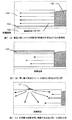
【発明が解決しようとする課題】
上述した金属元素を利用した結晶化の方法の概略を以下に示す。まず図5(A)に示すようにガラス基板501上に下地膜として酸化珪素膜502を成膜し、さらに非晶質珪素膜503を成膜する。
【0011】
次に酸素雰囲気中においてUV光を照射し、非晶質珪素膜の表面に極薄い酸化膜を形成する。これは、後に導入されるニッケルを含んだ溶液が非晶質珪素膜の表面から弾かれてしまうことを防ぐためである。
【0012】
次に酸化珪素膜でなるマスク504を形成する。そしてマスク504に開口505を形成する。次にニッケルを含んだ溶液を塗布し、さらにスピンコータによって、余分な溶液を吹き飛ばすことにより、506で示されるように溶液が微量に保持された状態を得る。(図5(B))
【0013】
次に加熱処理を施し、508で示されるような基板に平行な方向への結晶成長を行わせる。
【0014】
この際、酸化珪素膜でなるマスク504が存在している関係で成長が阻害されれてしまう。
【0015】
これは、マスク504と珪素膜との間に働く応力が関係する考えられるが詳細は不明である。
【0016】
この問題を回避するために、図5(B)の状態の後、マスク504を除去し、その後に加熱処理を行うことが考えられる。しかしその場合、ニッケルも同時に除去されてしまい、その後の結晶化に影響が出る。
【0017】
本明細書で開示する発明は、上述した基板に平行な方向への結晶成長における障害を取り除いた技術を提供することを課題とする。
【0018】
【課題を解決するための手段】
【0019】
本明細書で開示する発明の一つは、
絶縁表面を有する基板上に形成された非晶質珪素膜の一部を除去し、珪素の結晶化を助長する金属元素を導入するための領域を形成する工程と、
前記金属元素を添加するための領域に当該金属元素を選択的に保持させる工程と、
加熱処理を施し、前記金属元素添加領域から基板に平行な方向への結晶成長を行わす工程と、
を有することを特徴とする。
【0020】
また上記構成において、
当該金属元素の導入は、金属元素を含む溶液を塗布することにより行われ、
当該金属元素の選択的な保持は、珪素膜の前記溶液に対する撥水性を利用して行われることを特徴とする。
【0021】
また上記構成において、
結晶成長の際、結晶成長が行われる領域は、その表面が露呈していることを特徴とする。
【0022】
また他の発明として、
非晶質珪素膜の表面にから珪素の結晶化を助長する金属元素を導入する方法であって、
非晶質珪素膜の表面における疎水性を選択的に制御することのより、当該金属元素の導入量を位置的に制御することを特徴とする。
【0023】
これは、非晶質珪素膜の表面の疎水性を位置的に制御することにより、金属元素の導入を選択的に行うものである。
【0024】
例えば、非晶質珪素膜の一部に酸化膜を形成する。すると、その領域の濡れ性が向上する。そして、その状態で金属元素を含んだ溶液塗布することにより、その領域だけに当該金属元素を導入したり、その領域だけ当該金属元素の導入量を多くすることができる。
【0025】
珪素の結晶化を助長する金属元素しては、Niを利用することがその効果や再現性の点から最も好ましい。
【0026】
またこの金属元素としては、Fe、Co、Ni、Ru、Rh、Pd、Os、Ir、Pt、Cu、Auから選ばれた一種または複数種類の元素を利用することができる。
【0027】
出発膜としては、非晶質珪素膜の代わりに珪素化合物でなる非晶質膜を利用することができる。例えば、Six Ge1-x (0<x<1)で示される非晶質膜を用いることができる。
【0028】
【発明の実施の形態】
【0029】
まず、非晶質珪素膜203を成膜する。〔図2(A)〕
【0030】
そして、非晶質珪素膜203の一部を除去し、205で示される金属元素を導入するための領域を形成する。〔図2(B)〕
【0031】
次に非晶質珪素膜203に対して撥水性(疎水性)を示すニッケル元素を含んだ溶液(例えばニッケル酢酸塩溶液)を全面に塗布する。
【0032】
溶液に含ませる金属元素の量は、その溶液の種類にも依存するが、概略の傾向としてはニッケル量として溶液に対して200ppm〜1ppm、好ましくは50ppm〜1ppm(重量換算)とすることが望ましい。これは、結晶化終了後における膜中のニッケル濃度や耐フッ酸性に鑑みて決められる値である。
【0033】
図2(B)の状態においては、塗布された溶液は非晶質珪素膜の表面において弾かれる。
【0034】
そして、図2(C)に示すように非晶質珪素膜の一部が除去された領域(この領域では下地膜202が露呈している)のみに溶液が存在する状態となる。
【0035】
この状態では、図1(a)に示すように非晶質珪素膜103の側面に溶液150が存在した状態となる。ここで、100はガラス基板、102は下地の酸化珪素膜である。
【0036】
この状態で加熱処理を施すことにより、ニッケル元素が拡散し107(図2の場合は207)で示されるような基板に平行な方向への結晶成長が進行する。(図1(a),(図2(D))
【0037】
この結晶成長の際、珪素膜の表面には何も形成されていない(少なくとも人為的な成膜や処理は行われていない)ので、結晶成長がスムーズに進行する。
【0038】
上記の結晶化のための加熱処理の温度は、550℃〜650℃の温度から選択することが好ましい。
【0039】
これは、550℃よりも温度が低いと結晶化が進行せず、また650℃よりも温度が高いとニッケルの作用によらない結晶化が進行し、ニッケルの作用による結晶化を阻害するからである。
【0040】
非晶質珪素膜の一部を除去して得られる図2(B)205で示される形状(長さ、深さ、幅等の寸法)は、珪素膜の結晶性及び金属元素の量を制御する上で重要となる。
【0041】
また、図2に示す工程においては、図1(a)及び図2(B)で示す工程の以前に、非晶質珪素膜203を酸化させたり、非晶質珪素膜203上に他の膜を積層させないことが重要となる。
【0042】
図1(b)に示すように非晶質珪素膜103を酸化させ、酸化珪素膜104を形成した場合、酸化珪素膜では、十分な疎水性(撥水性)が得られないため、非晶質珪素膜上面に、溶液が残ってしまい、金属元素添加領域のみに金属元素を保持することが困難になる。
【0043】
更に、その後の工程である結晶化処理を行った場合、図1(b)のように、酸化膜と非晶質珪素膜の界面の影響により、結晶化が妨げられ、良好な結晶性を得ることができない。
【0044】
また図1(c)に示すように非晶質表面の意図しない領域からの結晶成長が進行し、特定の領域からの基板に平行な方向への結晶成長を阻害する状態が生じてしまう。(異なる領域からの結晶成長がぶつかると、そこで粒界が形成され結晶成長は停止する)
【0045】
以上のことから、金属元素を含んだ溶液を塗布する前に非晶質珪素膜表面の汚れ及び自然酸化膜をフッ酸処理等で除去することで、十分な撥水性を有する珪素膜表面を形成することが望ましい。
【0046】
また、非晶質珪素膜表面の汚れ及び自然酸化膜をフッ酸処理等で除去した後に酸化性雰囲気(例えば空気)に触れさせずに溶液を塗布し、さらに加熱処理する工程とすることが好ましい。
【0047】
【実施例】
〔実施例1〕
図2〜図4に本実施例の薄膜トランジスタの作製工程を示す。
【0048】
まず、石英基板200上に下地膜202として酸化珪素膜を30nmÅの厚さに成膜する。なお、石英基板の表面の平滑性が良く、また洗浄を十分にするのであれば、この下地膜202は特に必要ない。
【0049】
なお、絶縁基板としては石英基板を用いたが、その他に、ガラス基板、表面に絶縁膜膜を成膜した単結晶シリコン基板や多結晶シリコン基板を用いてもよい。
【0050】
次に結晶性珪素膜の出発膜となる非晶質珪素膜203を減圧熱CVD法でもって、60nmの厚さに成膜する。(図2(A))
【0051】
この非晶質珪素膜の厚さは、200nm以下とすることが好ましい。
【0052】
次に非晶質珪素膜に205で示されるような開口を形成する。開口205は、図面の奥行及び手前方向に長手方向を有する細長い長方形を有している。この開口205の幅は10μm以上とするのが適当である。またその端部は、後の工程で形成しようとする活性層の島領域よりも離れるように設計する。
【0053】
この開口において、下地膜である酸化珪素膜202が露呈する。
【0054】
次に、非晶質珪素膜表面の汚れ及び自然酸化膜をフッ酸処理等で除去する。
【0055】
そして重量換算で10ppmのニッケル元素を含んだ酢酸ニッケル溶液を塗布する。そして図示しないスピナーを用いてスピンドライを行い非晶質珪素膜上面に存在する余分な溶液を除去する。
【0056】
酢酸ニッケル塩溶液は、非晶質珪素膜に対して十分な撥水性を有している。こうして、ニッケル元素が図2(C)の点線206で示されるような状態で存在した状態が得られる。
【0057】
この状態では、開口205以外の領域では、ニッケル酢酸塩溶液は非晶質珪素膜の表面から弾かれている。そして、ニッケル元素が開口205の側壁において、非晶質珪素膜の一部に選択的に接して保持された状態が得られる。
【0058】
次に水素を3%含有した極力酸素を含まない窒素雰囲気中において、600℃、8時間の加熱処理を行う。すると、図2(D)の207で示されるように基板200に平行な方向への結晶成長が進行する。
【0059】
この結晶成長は、ニッケル元素が導入された開口205の領域(金属元素添加口)から基板に平行な方向へと進行する。
【0060】
この結晶成長により得られる横成長した結晶性珪素膜の表面は、従来の低温ポリシリコンや高温ポリシリコンに比較して非常に平滑性の良いものが得られる。これは、結晶粒界の延在する方向が概略そろっていることに起因すると考えられる。
【0061】
一般の多結晶珪素やポリシリコンと呼ばれる珪素膜は、その表面の凹凸は±10nm以上ある。しかし、本実施例で示すような横成長をさせた場合は、その表面の凹凸は±3nm以下であることが観察されている。この凹凸は、ゲイト絶縁膜との間の界面特性を悪化させるものであり、極力小さいものであることが好ましい。
【0062】
上記の結晶化のために加熱処理条件においては、この横成長を100μm以上にわたって行わすことができる。
【0063】
図2(D)に示す状態を得た後、レーザー光の照射を行なってもよい。即ち、レーザー光の照射により、さらに結晶化を助長させてもよい。このレーザー光の照射は、膜中に存在するニッケル元素の固まりを分散させ、後にニッケル元素を除去し易くする効果を有している。なお、この段階でレーザー光の照射を行っても、さらに横成長が進行することはない。
【0064】
レーザー光としては、紫外領域の波長を有するエキシマレーザーを利用することができる。例えば、KrFエキシマレーザー(波長248nm)やXeClエキシマレーザー(波長308nm)を利用することができる。
【0065】
次にハロゲン元素を含有した酸素雰囲気、例えばHClを3体積%含んだ酸素雰囲気中において、950℃の加熱処理を行い、図示しない熱酸化膜を200Åの厚さに成膜する。この熱酸化膜の形成に従い、珪素膜の膜厚は100Å程度その膜厚が減少する。即ち、珪素膜の膜厚は、500Å程度となる。
【0066】
この工程においては、熱酸化膜の形成に従い、膜中の不安定な結合状態を有する珪素元素が熱酸化膜の形成に利用される。そして、膜中の欠陥が減少し、より高い結晶性を得ることができる。
【0067】
また同時に熱酸化膜の形成および塩素の作用により膜中よりニッケル元素のゲッタリングが行われる。
【0068】
熱酸化膜を形成したら、図示しない熱酸化膜を除去する。こうして、ニッケル元素の含有濃度を減少させた結晶性珪素膜を得る。こうして得られた結晶性珪素膜は、一方向に結晶構造が延在した(この方向は結晶成長方向に一致する)構造を有している。即ち、細長い円柱状の結晶体が複数の一方向に延在した結晶粒界を介して、複数平行に並んでいるような構造を有している。
【0069】
次にパターニングを行うことにより、横成長領域でなるパターンを形成する。この島状の領域301が後にTFTの活性層となる。(図3(E))
【0070】
ここでは、ソース領域とドレイン領域とを結ぶ方向と結晶成長方向とが一致または概略一致するようにパターンの位置取りを行う。こうすることで、キャリアの移動する方向と結晶格子が連続して延在する方向とを合わせることができ、結果として高い特性のTFTを得ることができる。
【0071】
そして、301でなるパターンを形成後にプラズマCVD法で酸化珪素膜315を500Åの厚さに成膜する。(図3(F))
【0072】
さらに熱酸化法により熱酸化膜311を300Åの厚さに成膜する。こうしてCVD酸化珪素膜315と熱酸化膜311とでなる厚さ800Åのゲイト絶縁膜を得る。(図3(G))
【0073】
ゲイト絶縁膜を形成することにより、活性層となるパターン301の膜厚は、350Åとなる。これは、300Å厚の熱酸化膜311の成膜により、さらに活性層パターンの表面が150Åの厚さでもって目減りするからである。
【0074】
次にゲイト電極を形成するためのアルミニウム膜をスパッタ法で4000Åの厚さに成膜する。このアルミニウム膜中には、スカンジウムを0.2 重量%含有させる。
【0075】
アルミニウム膜中にスカンジウムを含有させるのは、後の工程において、ヒロックやウィスカーが発生することを抑制するためである。ヒロックやウィスカーというのは、加熱の際のアルミニウムの異常成長に起因する針状あるいは刺状の突起部のことである。
【0076】
ゲイト電極を形成するための材料として、アルミウニム以外にタンタル(Ta)、高濃度にリン(P)がドープされた多結晶シリコン、タングステンのシリサイド(WSi)、またはリンドープされた多結晶シリコンとタングステンのシリサイドの積層また混成した構造を利用することもできる。
【0077】
アルミニウム膜を成膜したら、図示しない緻密な陽極酸化膜を形成する。この陽極酸化膜は、3%の酒石酸を含んだエチレングルコール溶液を電解溶液とし、アルミニウム膜を陽極、白金を陰極として行う。この工程においては、アルミニウム膜上に緻密な膜質を有する陽極酸化膜を100Åの厚さに成膜する。
【0078】
この図示しない陽極酸化膜は、後に形成されるレジストマスクとの密着性を向上させる役割を有している。
【0079】
この陽極酸化膜の膜厚は、陽極酸化時の印加電圧によって制御することができる。
【0080】
次にレジストマスク322を形成する。そしてこのレジストマスクを利用して、アルミニウム膜を318で示されるパターンにパターニングする。こうして図3(H)に示す状態を得る。
【0081】
ここで再度の陽極酸化を行う。ここでは、3%のシュウ酸水溶液を電解溶液として用いる。この電解溶液中において、アルミニウムのパターン318を陽極とした陽極酸化を行うことにより、多孔質状の陽極酸化膜が形成される。
【0082】
この工程においては、上部に密着性の高いレジストマスク322が存在する関係で、アルミニウムパターンの側面に選択的に陽極酸化膜419が形成される。(図4(I))
【0083】
この陽極酸化膜は、その膜厚を数μmまで成長させることができる。ここでは、その膜厚を6000Åとする。なお、その成長距離は、陽極酸化時間によって制御することができる。
【0084】
そしてレジストマスク322を除去する。次に再度の緻密な陽極酸化膜の形成を行う。即ち、前述した3%の酒石酸を含んだエチレングルコール溶液を電解溶液とした陽極酸化を再び行う。
【0085】
この工程においては、多孔質状の陽極酸化膜419中に電解溶液が進入する関係から、420で示されるように緻密な膜質を有する陽極酸化膜が形成される。
【0086】
この緻密な陽極酸化膜420の膜厚は1000Åとする。この膜厚の制御は印加電圧によって行う。
【0087】
ここで、露呈した酸化珪素膜315をエッチングする。またCVD酸化酸化珪素膜315及び熱酸化膜311とでなるゲイト絶縁膜をエッチングする。このエッチングはドライエッチングを利用する。
【0088】
こうして図4(J)に示す状態を得る。そして酢酸と硝酸とリン酸とを混合した混酸を用いて多孔質状の陽極酸化膜419を除去する。
【0089】
図4(J)に示す状態を得たら、不純物イオンの注入を行う。ここでは、Nチャネル型の薄膜トランジスタを作製するためにP(リン)イオンの注入をプラズマドーピング法でもって行う。
【0090】
この工程においては、ヘビードープがされる430と434の領域とライトドープがされる431と433の領域が形成される。これは、残存した酸化珪素膜315が半透過なマスクとして機能し、注入されたイオンの一部がそこで遮蔽されるからである。
【0091】
本実施例においてもオフセットゲイト領域は形成されているが、その寸法が小さいのでその存在による寄与が小さく、また図面が煩雑になるので図中には記載していない。
【0092】
ここで、433で示されるのが、LDD(ライトドープドレイン)領域と称される領域である。(図4(J))
【0093】
なお、緻密な陽極酸化膜420の膜厚を2000Å以上というように厚くした場合、その膜厚でもってチャネル形成領域432の外側にオフセットゲイト領域を形成することができる。
【0094】
〔実施例2〕
本実施例は、非晶質珪素膜の表面の疎水性を選択的に制御することのより、結晶性の異なるTFTを選択的に作製する例を示す。
【0095】
次に層間絶縁膜440として酸化珪素膜、または窒化珪素膜、またはその積層膜を形成する。層間絶縁膜としては、酸化珪素膜または窒化珪素膜上に樹脂材料でなる層を用いてもよい。
【0096】
そしてコンタクトホールの形成を行い、ソース電極441とドレイン電極442の形成を行う。こうして図4(K)に示す薄膜トランジスタが完成する。
【0097】
〔実施例2〕
本実施例は、非晶質珪素膜の表面の疎水性を選択的に制御することのより、化粧性の異なるTFTを選択的に作製する例を示す。
【0098】
即ち、非晶質珪素膜の一部に酸化膜を形成することにより、その領域の濡れ性を向上させ(即ち、疎水性を低下させる)、その領域のみに選択的に多くのニッケル元素を導入する場合の例を示す。
【0099】
一般的に金属元素の濃度を高くした場合、高い結晶性が得られ、得られるTFTの移動度は大きなものとなる。しかし、特性不安定性やOFF電流の値は大きなものとなる。
【0100】
また、一般論としてPチャネル型のTFT(PTFT)は、特性が安定しているが、移動度が小さい。他方、Nチャネル型のTFT(NTFT)は、移動度が大きいが、ホットキャリア効果のために特性が不安定であるという傾向がある。
【0101】
そこで、本実施例では、Pチャネル型のTFTを構成する結晶性珪素膜は、高い濃度での金属元素を利用して作製し、他方Nチャネル型のTFTを構成する結晶性珪素膜は、低い濃度での金属元素を利用して作製する。
【0102】
図6に本実施例の作製工程を示す。まずガラス基板601(または石英基板)上に下地膜として酸化珪素膜602を成膜する。
【0103】
次に非晶質珪素膜603を減圧熱CVD法で成膜する。
【0104】
次に選択的に極薄い酸化膜(図示せず)を全体に成膜、さらに選択的に酸化膜604を成膜する。ここでは、酸化雰囲気中でのUV光の照射により酸化膜を成膜する。酸化膜を成膜方法としては、オゾン水等の酸化作用の溶液を用いてもよい。
【0105】
こうして図6(A)に示す状態を得る。次にニッケル酢酸塩溶液を塗布する。この時、酸化膜604が成膜されている領域は、その表面の疎水性が低下しているので、そこには他の領域に比較してより多くのニッケル元素が接して保持される状態となる。(図6(B))
【0106】
そして、それに対応して、得られる結晶性も異なるものとなる。こうして高い結晶性を有する領域606と、それに比較して結晶性が低い領域607とを得る。(図6(C))
【0107】
次に加熱処理を施す。この加熱処理は、窒素雰囲気中において、600℃、4時間行う。
【0108】
この際、膜の全体が結晶化する。この結晶化の際、非晶質珪素膜の表面に接して存在しているニッケル元素の量(密度)は、酸化膜605が成膜されている領域では多く、他の領域ではそれに比較して少ない。
【0109】
そして、それに対応して、得られる結晶性も異なるものとなる。こうして他界結晶性を有する領域606と、それに比較して結晶性が低い領域607とを得る。(図6(C))
【0110】
次にパターニングを行い、608と609で示される領域を形成する。ここで、領域608の結晶性は、領域609の結晶性よりも高い。これらの領域は、後にTFTの活性層となる。(図6(D))
【0111】
次にゲイト絶縁膜600を形成する。そして、アルミニウムでなるゲイト電極610、612を形成する。ゲイト電極の周囲には陽極酸化膜611、613を形成する。
【0112】
次に選択的にリンおよびボロンのドーピングを行うことにより、PTFTのソース領域614、チャネル領域615、ドレイン領域616を自己整合的に形成する。(図6(E))
【0113】
また同時にNTFTのソース領域617、チャネル領域618、ドレイン領域619を自己整合的に形成する。(図6(E))
【0114】
次に層間絶縁膜620を成膜し、さらにコンタクトホールを形成して、PTFTのソース電極621、ドレイン電極622を形成する。また、NTFTのソース電極623、ドレイン電極624を形成する。
【0115】
こうして、PTFTとNTFTとを得る。この構成においては、PTFTを構成する活性層の結晶性がNTFTを構成する活性層の結晶性よりも高い。
【0116】
従って、相対的にPTFTの移動度を高くすることができる。PTFTの特性はNTFTに比較すれば安定しているので、ニッケル元素濃度が多少高くなっても総合的には問題とはならない。
【0117】
他方、NTFTにおいては、活性層中におけるニッケル元素の濃度を減らし、特性の安定性を高めることができる。
【0118】
こうして、PTFTとNTFTの移動度の違いを是正し、さらに特性の安定の違いを是正することができる。
【0119】
【発明の効果】
本明細書で開示する発明は、珪素膜が有する撥水性を利用することにより、珪素の結晶化を助長する金属元素を含有する溶液を塗布する際に、選択的な塗布を実現し、そのことにより、基板に平行な方向への結晶成長を行わせることができる。このような構成は、結晶成長領域の上部に結晶成長を阻害するマスクが形成されていないので、結晶成長が妨げられず、質の高い結晶性領域を得ることができる。
【0120】
この技術を利用すると、高い特性を有するTFTを高い再現性でもって、また特性をそろえて得ることができる。
【0121】
本明細書で開示した発明は、透過型、反射型のアクティブマトリクス型の液晶表示装置の、アクティブマトリクス回路と同一基板に形成される周辺回路を構成するのみでなく、他にEL(エレクトロルミネセンス)素子を用いた表示装置、その他薄膜トランジスタを用いた種々の回路にて利用することができる。
【0122】
また、本明細書で開示した発明は、薄膜トランジスタを利用した各種集積回路、及びその各種集積回路を利用した装置の作製に利用することができる。このような装置としては、例えば携帯型の情報処理端末やビデオカメラを挙げることができる。
【図面の簡単な説明】
【図1】 本発明の結晶化時における金属元素の添加を行う開口付近を示す断面図
【図2】 薄膜トランジスタの作製工程を示す図
【図3】 薄膜トランジスタの作製工程を示す図
【図4】 薄膜トランジスタの作製工程を示す図
【図5】 従来の技術における結晶化方法を示す図。
【図6】 薄膜トランジスタの作製工程を示す図。
【符号の説明】
100 絶縁基板
102 下地膜
103 非晶質珪素膜
104 酸化珪素膜
107 結晶成長方向
150 金属元素添加口に保持された化合物溶液
151 非晶質珪素膜上面に残留した化合物溶液
200 石英基板
202 下地膜
203 非晶質珪素膜
205 非晶質珪素膜の開口(金属元素添加口)
206 基板に接して保持されたニッケル元素
301 活性層(半導体)の島領域
311 熱酸化膜
315 酸化珪素膜(ゲイト絶縁膜)
318 アルミニウム膜
322 レジストマスク
419 多孔質な酸化膜
420 緻密な酸化膜
430 ソース領域
431 低濃度不純物領域
432 チャネル領域
433 低濃度不純物領域(LDD領域)
434 ドレイン領域
440 層間絶縁膜
441 ソース電極
442 ドレイン電極[0001]
BACKGROUND OF THE INVENTION
The invention disclosed in this specification relates to a method for manufacturing a semiconductor device using a crystalline semiconductor.
[0002]
[Prior art]
A thin film transistor (hereinafter referred to as TFT) using a thin film semiconductor is known. This TFT is formed by forming a thin film semiconductor on a substrate and using this thin film semiconductor. This TFT is used in various integrated circuits, and is particularly attracting attention as a switching element provided with each pixel of an electro-optical device, particularly an active matrix liquid crystal display device, and a driver element formed in a peripheral circuit portion. .
[0003]
Conventionally, amorphous silicon films have been used as thin film semiconductors used in TFTs, but attempts have been made to use crystalline silicon films (crystalline silicon films) in order to obtain higher performance. Yes.
[0004]
A TFT using a crystalline silicon film can operate at a high speed of two orders of magnitude or more compared to a TFT using an amorphous silicon film, and the periphery of a liquid crystal display device that has been configured by an external IC circuit so far. The driver circuit can be manufactured over the same substrate as the active matrix circuit.
[0005]
A conventional crystalline silicon film is obtained by forming an amorphous silicon film by a plasma CVD method or a low pressure thermal CVD method and then crystallizing the film by heat treatment or laser light irradiation.
[0006]
However, the method of crystallization by heating has the feature that a crystalline silicon thin film can be obtained over a wide area,
(1) A high heating temperature is required. (Use of glass substrate is difficult)
(2) The crystallinity obtained is not sufficient.
Have the problem.
[0007]
On the other hand, the method using laser light irradiation has an advantage that a glass substrate can be used as a substrate, but has a problem that it is difficult to process productivity and a large area.
[0008]
[Background of the present invention]
Therefore, the present inventors have added a metal element that promotes crystallization, such as nickel, palladium, and lead, to the amorphous silicon film, and obtains a crystalline silicon film by heat treatment at a temperature lower than that of the prior art. Developed. (Refer to Japanese Patent Laid-Open No. 7-130652)
[0009]
By this method, the crystallization speed can be increased and not only can be crystallized in a short time, but also over a wide area compared to the conventional crystallization method by heating alone or crystallization of an amorphous film only by laser light irradiation. High crystallinity can be obtained uniformly.
[0010]
[Problems to be solved by the invention]
An outline of the crystallization method using the metal element described above is shown below. First, as shown in FIG. 5A, a
[0011]
Next, UV light is irradiated in an oxygen atmosphere to form an extremely thin oxide film on the surface of the amorphous silicon film. This is to prevent the nickel-containing solution introduced later from being repelled from the surface of the amorphous silicon film.
[0012]
Next, a
[0013]
Next, heat treatment is performed, and crystal growth is performed in a direction parallel to the substrate as indicated by 508.
[0014]
At this time, the growth is hindered due to the presence of the
[0015]
This is considered to be related to the stress acting between the
[0016]
In order to avoid this problem, it is conceivable to remove the
[0017]
An object of the invention disclosed in this specification is to provide a technique that eliminates the obstacle in crystal growth in a direction parallel to the substrate described above.
[0018]
[Means for Solving the Problems]
[0019]
One of the inventions disclosed in this specification is:
Removing a part of the amorphous silicon film formed over the substrate having an insulating surface and forming a region for introducing a metal element that promotes crystallization of silicon;
Selectively holding the metal element in a region for adding the metal element;
Performing a heat treatment, and performing crystal growth in a direction parallel to the substrate from the metal element addition region;
It is characterized by having.
[0020]
In the above configuration,
The introduction of the metal element is performed by applying a solution containing the metal element,
The selective retention of the metal element is performed using water repellency of the silicon film with respect to the solution.
[0021]
In the above configuration,
During crystal growth, the region where crystal growth is performed is characterized in that the surface is exposed.
[0022]
As another invention,
A method of introducing a metal element that promotes crystallization of silicon from the surface of an amorphous silicon film,
The introduction amount of the metal element is controlled in position by selectively controlling the hydrophobicity on the surface of the amorphous silicon film.
[0023]
This selectively introduces a metal element by positionally controlling the hydrophobicity of the surface of the amorphous silicon film.
[0024]
For example, an oxide film is formed on part of the amorphous silicon film. Then, the wettability of the region is improved. Then, by applying a solution containing a metal element in that state, the metal element can be introduced only into the region, or the amount of the metal element introduced can be increased only in the region.
[0025]
As a metal element for promoting crystallization of silicon, it is most preferable to use Ni from the viewpoint of its effect and reproducibility.
[0026]
Further, as this metal element, one or more kinds of elements selected from Fe, Co, Ni, Ru, Rh, Pd, Os, Ir, Pt, Cu, and Au can be used.
[0027]
As the starting film, an amorphous film made of a silicon compound can be used instead of the amorphous silicon film. For example, an amorphous film represented by Si x Ge 1-x (0 <x <1) can be used.
[0028]
DETAILED DESCRIPTION OF THE INVENTION
[0029]
First, an
[0030]
Then, a part of the
[0031]
Next, a solution containing nickel element exhibiting water repellency (hydrophobicity) (for example, nickel acetate solution) is applied to the entire surface of the
[0032]
The amount of the metal element contained in the solution depends on the type of the solution, but as a general tendency, it is desirable that the nickel amount is 200 ppm to 1 ppm, preferably 50 ppm to 1 ppm (weight conversion) with respect to the solution. . This is a value determined in view of the nickel concentration in the film and the hydrofluoric acid resistance after crystallization is completed.
[0033]
In the state of FIG. 2B, the applied solution is repelled on the surface of the amorphous silicon film.
[0034]
Then, as shown in FIG. 2C, the solution exists only in a region where a part of the amorphous silicon film is removed (in this region, the
[0035]
In this state, the
[0036]
By performing heat treatment in this state, nickel element diffuses and crystal growth proceeds in a direction parallel to the substrate as indicated by 107 (207 in the case of FIG. 2). (FIG. 1 (a), (FIG. 2 (D))
[0037]
During this crystal growth, nothing is formed on the surface of the silicon film (at least no artificial film formation or treatment is performed), so that the crystal growth proceeds smoothly.
[0038]
The temperature of the heat treatment for crystallization is preferably selected from temperatures of 550 ° C to 650 ° C.
[0039]
This is because if the temperature is lower than 550 ° C., crystallization does not proceed, and if the temperature is higher than 650 ° C., crystallization is not caused by the action of nickel, and the crystallization due to the action of nickel is inhibited. is there.
[0040]
The shape (length, depth, width, etc.) shown in FIG.
[0041]
In the process shown in FIG. 2, the
[0042]
When the
[0043]
Further, when the subsequent crystallization process is performed, the crystallization is hindered by the influence of the interface between the oxide film and the amorphous silicon film as shown in FIG. I can't.
[0044]
In addition, as shown in FIG. 1C, crystal growth from an unintended region of the amorphous surface proceeds, and a state of inhibiting crystal growth from a specific region in a direction parallel to the substrate occurs. (If crystal growth from different areas collides, a grain boundary is formed and crystal growth stops.)
[0045]
From the above, the silicon film surface with sufficient water repellency is formed by removing dirt and natural oxide film on the amorphous silicon film surface by hydrofluoric acid treatment etc. before applying the solution containing metal element It is desirable to do.
[0046]
In addition, it is preferable that the surface of the amorphous silicon film and the natural oxide film are removed by hydrofluoric acid treatment or the like, and then the solution is applied without being exposed to an oxidizing atmosphere (for example, air), followed by heat treatment. .
[0047]
【Example】
[Example 1]
2 to 4 show a manufacturing process of the thin film transistor of this embodiment.
[0048]
First, a silicon oxide film is formed as a
[0049]
Note that although a quartz substrate is used as the insulating substrate, a glass substrate or a single crystal silicon substrate or a polycrystalline silicon substrate having an insulating film formed on the surface may be used.
[0050]
Next, an
[0051]
The thickness of the amorphous silicon film is preferably 200 nm or less.
[0052]
Next, an opening as indicated by 205 is formed in the amorphous silicon film. The
[0053]
In this opening, the
[0054]
Next, the surface of the amorphous silicon film and the natural oxide film are removed by hydrofluoric acid treatment or the like.
[0055]
Then, a nickel acetate solution containing 10 ppm of nickel element in terms of weight is applied. Then, spin drying is performed using a spinner (not shown) to remove excess solution existing on the upper surface of the amorphous silicon film.
[0056]
The nickel acetate salt solution has sufficient water repellency for the amorphous silicon film. In this way, a state is obtained in which the nickel element is present as shown by the dotted
[0057]
In this state, in a region other than the
[0058]
Next, heat treatment is performed at 600 ° C. for 8 hours in a nitrogen atmosphere containing 3% hydrogen and containing as little oxygen as possible. Then, crystal growth in a direction parallel to the
[0059]
This crystal growth proceeds in the direction parallel to the substrate from the region of the
[0060]
The surface of the laterally grown crystalline silicon film obtained by this crystal growth has a very smooth surface compared to conventional low-temperature polysilicon and high-temperature polysilicon. This is considered due to the fact that the extending directions of the crystal grain boundaries are roughly aligned.
[0061]
A general silicon film called polycrystalline silicon or polysilicon has a surface roughness of ± 10 nm or more. However, when lateral growth as shown in this example is performed, it has been observed that the surface irregularities are ± 3 nm or less. This unevenness deteriorates the interface characteristics with the gate insulating film, and is preferably as small as possible.
[0062]
In the heat treatment conditions for the above crystallization, this lateral growth can be performed over 100 μm or more.
[0063]
After obtaining the state shown in FIG. 2D, laser light irradiation may be performed. That is, crystallization may be further promoted by laser light irradiation. This laser light irradiation has the effect of dispersing the mass of nickel elements present in the film and facilitating removal of the nickel elements later. Note that even if laser light irradiation is performed at this stage, the lateral growth does not proceed further.
[0064]
As the laser light, an excimer laser having a wavelength in the ultraviolet region can be used. For example, a KrF excimer laser (wavelength 248 nm) or a XeCl excimer laser (wavelength 308 nm) can be used.
[0065]
Next, heat treatment is performed at 950 ° C. in an oxygen atmosphere containing a halogen element, for example, an oxygen atmosphere containing 3% by volume of HCl, and a thermal oxide film (not shown) is formed to a thickness of 200 mm. As the thermal oxide film is formed, the film thickness of the silicon film decreases by about 100 mm. That is, the thickness of the silicon film is about 500 mm.
[0066]
In this step, silicon elements having an unstable bonding state in the film are used for forming the thermal oxide film in accordance with the formation of the thermal oxide film. And the defect in a film | membrane reduces and higher crystallinity can be obtained.
[0067]
At the same time, nickel elements are gettered from the film by the formation of a thermal oxide film and the action of chlorine.
[0068]
After forming the thermal oxide film, the thermal oxide film (not shown) is removed. In this way, a crystalline silicon film having a reduced nickel element concentration is obtained. The crystalline silicon film thus obtained has a structure in which the crystal structure extends in one direction (this direction coincides with the crystal growth direction). That is, it has a structure in which a plurality of elongated cylindrical crystals are arranged in parallel through a plurality of crystal grain boundaries extending in one direction.
[0069]
Next, patterning is performed to form a pattern composed of laterally grown regions. This island-shaped
[0070]
Here, the pattern is positioned so that the direction connecting the source region and the drain region and the crystal growth direction match or approximately match. By doing so, the direction in which the carriers move and the direction in which the crystal lattice continuously extends can be matched, and as a result, a TFT with high characteristics can be obtained.
[0071]
Then, after the
[0072]
Further, a
[0073]
By forming the gate insulating film, the film thickness of the
[0074]
Next, an aluminum film for forming a gate electrode is formed to a thickness of 4000 mm by sputtering. This aluminum film contains 0.2% by weight of scandium.
[0075]
The reason why scandium is contained in the aluminum film is to suppress generation of hillocks and whiskers in the subsequent process. Hillocks and whiskers are needle-like or stab-like protrusions resulting from abnormal growth of aluminum during heating.
[0076]
As a material for forming the gate electrode, in addition to aluminum, tantalum (Ta), polycrystalline silicon doped with phosphorus (P) at a high concentration, tungsten silicide (WSi), or phosphorous-doped polycrystalline silicon and tungsten A stacked or mixed structure of silicide can also be used.
[0077]
When the aluminum film is formed, a dense anodic oxide film (not shown) is formed. The anodic oxide film is formed using an ethylene glycol solution containing 3% tartaric acid as an electrolytic solution, an aluminum film as an anode, and platinum as a cathode. In this step, an anodic oxide film having a dense film quality is formed on the aluminum film to a thickness of 100 mm.
[0078]
This anodic oxide film (not shown) has a role of improving adhesion with a resist mask to be formed later.
[0079]
The film thickness of this anodic oxide film can be controlled by the applied voltage during anodic oxidation.
[0080]
Next, a resist
[0081]
Here, anodic oxidation is performed again. Here, a 3% oxalic acid aqueous solution is used as the electrolytic solution. In this electrolytic solution, a porous anodic oxide film is formed by performing anodization using the
[0082]
In this step, an
[0083]
This anodic oxide film can be grown to a thickness of several μm. Here, the film thickness is 6000 mm. The growth distance can be controlled by the anodic oxidation time.
[0084]
Then, the resist
[0085]
In this step, an anodic oxide film having a dense film quality is formed as indicated by 420 because the electrolytic solution enters the porous
[0086]
The dense
[0087]
Here, the exposed
[0088]
In this way, the state shown in FIG. Then, the porous
[0089]
After obtaining the state shown in FIG. 4J, impurity ions are implanted. Here, in order to manufacture an N-channel thin film transistor, P (phosphorus) ions are implanted by a plasma doping method.
[0090]
In this step,
[0091]
In this embodiment, the offset gate region is formed, but since the size thereof is small, the contribution due to its existence is small, and the drawing becomes complicated, so it is not shown in the drawing.
[0092]
Here, a region denoted by 433 is a region called an LDD (lightly doped drain) region. (Fig. 4 (J))
[0093]
When the thickness of the dense
[0094]
[Example 2]
This embodiment shows an example in which TFTs having different crystallinities are selectively manufactured by selectively controlling the hydrophobicity of the surface of an amorphous silicon film.
[0095]
Next, a silicon oxide film, a silicon nitride film, or a stacked film thereof is formed as the
[0096]
Then, contact holes are formed, and a
[0097]
[Example 2]
This embodiment shows an example in which TFTs having different cosmetic properties are selectively manufactured by selectively controlling the hydrophobicity of the surface of an amorphous silicon film.
[0098]
That is, by forming an oxide film on a part of the amorphous silicon film, the wettability of the region is improved (that is, the hydrophobicity is lowered), and a large amount of nickel element is selectively introduced only into the region. An example of the case is shown.
[0099]
In general, when the concentration of the metal element is increased, high crystallinity is obtained, and the mobility of the obtained TFT is increased. However, the characteristic instability and the value of the OFF current are large.
[0100]
In general, a P-channel TFT (PTFT) has stable characteristics but low mobility. On the other hand, an N-channel TFT (NTFT) has high mobility, but tends to have unstable characteristics due to the hot carrier effect.
[0101]
Therefore, in this embodiment, the crystalline silicon film constituting the P-channel TFT is manufactured using a metal element at a high concentration, while the crystalline silicon film constituting the N-channel TFT is low. Fabricate using metal element at concentration.
[0102]
FIG. 6 shows a manufacturing process of this example. First, a silicon oxide film 602 is formed as a base film on a glass substrate 601 (or a quartz substrate).
[0103]
Next, an
[0104]
Next, an extremely thin oxide film (not shown) is selectively formed on the entire surface, and an oxide film 604 is further selectively formed. Here, an oxide film is formed by irradiation with UV light in an oxidizing atmosphere. As a method for forming the oxide film, an oxidizing solution such as ozone water may be used.
[0105]
In this way, the state shown in FIG. Next, a nickel acetate solution is applied. At this time, since the hydrophobicity of the surface of the region where the oxide film 604 is formed is reduced, more nickel element is held in contact therewith than the other regions. Become. (Fig. 6 (B))
[0106]
Correspondingly, the crystallinity obtained is also different. Thus, a region 606 having high crystallinity and a region 607 having lower crystallinity than that are obtained. (Fig. 6 (C))
[0107]
Next, heat treatment is performed. This heat treatment is performed at 600 ° C. for 4 hours in a nitrogen atmosphere.
[0108]
At this time, the entire film is crystallized. At the time of crystallization, the amount (density) of nickel element existing in contact with the surface of the amorphous silicon film is large in the region where the oxide film 605 is formed, and compared with that in other regions. Few.
[0109]
Correspondingly, the crystallinity obtained is also different. In this way, a region 606 having other-field crystallinity and a region 607 having lower crystallinity than that are obtained. (Fig. 6 (C))
[0110]
Next, patterning is performed to form regions indicated by 608 and 609. Here, the crystallinity of the region 608 is higher than the crystallinity of the region 609. These regions will later become the active layer of the TFT. (Fig. 6 (D))
[0111]
Next, a gate insulating film 600 is formed. Then, gate electrodes 610 and 612 made of aluminum are formed. Anodized films 611 and 613 are formed around the gate electrode.
[0112]
Next, the source region 614, the channel region 615, and the drain region 616 of the PTFT are formed in a self-alignment manner by selectively doping with phosphorus and boron. (Fig. 6 (E))
[0113]
At the same time, the NTFT source region 617, channel region 618, and drain region 619 are formed in a self-aligned manner. (Fig. 6 (E))
[0114]
Next, an
[0115]
Thus, PTFT and NTFT are obtained. In this configuration, the crystallinity of the active layer constituting the PTFT is higher than the crystallinity of the active layer constituting the NTFT.
[0116]
Therefore, the mobility of PTFT can be relatively increased. Since the characteristics of PTFT are stable as compared with NTFT, even if the nickel element concentration is somewhat higher, there is no problem overall.
[0117]
On the other hand, in NTFT, the density | concentration of the nickel element in an active layer can be reduced and the stability of a characteristic can be improved.
[0118]
In this way, the difference in mobility between PTFT and NTFT can be corrected, and further, the difference in characteristic stability can be corrected.
[0119]
【The invention's effect】
The invention disclosed in this specification realizes selective application when applying a solution containing a metal element that promotes crystallization of silicon by utilizing the water repellency of a silicon film. Thus, crystal growth in a direction parallel to the substrate can be performed. In such a configuration, since a mask that inhibits crystal growth is not formed above the crystal growth region, crystal growth is not hindered, and a high-quality crystalline region can be obtained.
[0120]
If this technology is used, a TFT having high characteristics can be obtained with high reproducibility and uniform characteristics.
[0121]
The invention disclosed in this specification not only constitutes a peripheral circuit formed on the same substrate as the active matrix circuit of the transmissive and reflective active matrix liquid crystal display device, but also EL (electroluminescence). ) It can be used in display devices using elements and other various circuits using thin film transistors.
[0122]
The invention disclosed in this specification can be used for manufacturing various integrated circuits using thin film transistors and devices using the various integrated circuits. Examples of such an apparatus include a portable information processing terminal and a video camera.
[Brief description of the drawings]
1 is a cross-sectional view showing the vicinity of an opening to which a metal element is added during crystallization according to the present invention. FIG. 2 is a diagram showing a manufacturing process of a thin film transistor. FIG. 3 is a diagram showing a manufacturing process of a thin film transistor. FIG. 5 is a diagram showing a crystallization method in the prior art.
6A and 6B illustrate a manufacturing process of a thin film transistor.
[Explanation of symbols]
100 Insulating
206
318
434
Claims (7)
前記非晶質珪素膜の一部を除去して、前記非晶質珪素膜に開口を形成し、
前記非晶質珪素膜表面の汚れ及び自然酸化膜をフッ酸処理により除去して撥水性とし、
前記非晶質珪素膜の開口に、珪素の結晶化を助長する金属元素を導入して、前記開口の側面に前記金属元素を選択的に接して保持させ、
前記非晶質珪素膜を加熱することにより、前記開口の側面から、前記基板に対して平行な方向に結晶成長を行わせ、
前記金属元素は、前記金属元素を含む溶液を前記非晶質珪素膜に塗布することにより導入され、
前記金属元素は、前記非晶質珪素膜の表面における前記溶液に対する撥水性を利用して前記開口に選択的に接して保持されることを特徴とする半導体装置の作製方法。Forming an amorphous silicon film over a substrate having an insulating surface;
Removing part of the amorphous silicon film to form an opening in the amorphous silicon film;
The surface of the amorphous silicon film and the natural oxide film are removed by hydrofluoric acid treatment to make it water repellent.
Introducing a metal element that promotes crystallization of silicon into the opening of the amorphous silicon film, selectively holding the metal element in contact with the side surface of the opening,
By heating the amorphous silicon film, crystal growth is performed in a direction parallel to the substrate from the side surface of the opening,
The metal element is introduced by applying a solution containing the metal element to the amorphous silicon film,
The method for manufacturing a semiconductor device, wherein the metal element is selectively held in contact with the opening by utilizing water repellency with respect to the solution on the surface of the amorphous silicon film.
前記非晶質珪素膜の一部を除去して、前記非晶質珪素膜に開口を形成し、
前記非晶質珪素膜表面の汚れ及び自然酸化膜をフッ酸処理により除去して撥水性とし、
前記非晶質珪素膜の開口に、珪素の結晶化を助長する金属元素を導入して、前記開口の側面に前記金属元素を選択的に接して保持させ、
前記非晶質珪素膜を加熱することにより、前記開口の側面から、前記基板に対して平行な方向に結晶成長を行わせ、
前記金属元素は、前記金属元素を含む溶液を前記非晶質珪素膜に塗布することにより導入され、
前記金属元素は、前記非晶質珪素膜の表面における前記溶液に対する撥水性を利用して前記開口に選択的に接して保持され、
前記金属元素の導入量は、前記開口の形状によって制御されることを特徴とする半導体装置の作製方法。Forming an amorphous silicon film over a substrate having an insulating surface;
Removing part of the amorphous silicon film to form an opening in the amorphous silicon film;
The surface of the amorphous silicon film and the natural oxide film are removed by hydrofluoric acid treatment to make it water repellent.
Introducing a metal element that promotes crystallization of silicon into the opening of the amorphous silicon film, selectively holding the metal element in contact with the side surface of the opening,
By heating the amorphous silicon film, crystal growth is performed in a direction parallel to the substrate from the side surface of the opening,
The metal element is introduced by applying a solution containing the metal element to the amorphous silicon film,
The metal element is held in selective contact with the opening using water repellency with respect to the solution on the surface of the amorphous silicon film,
The method for manufacturing a semiconductor device, wherein the amount of the metal element introduced is controlled by the shape of the opening.
前記結晶成長により得られた結晶性珪素膜をパターニングして島状領域を形成し、
前記島状領域にゲイト絶縁膜及びゲイト電極を形成し、
前記島状領域に不純物を導入して、ソース領域、ドレイン領域及びチャネル形成領域を形成することを特徴とする半導体装置の作製方法。In claim 1 or claim 2,
Patterning the crystalline silicon film obtained by the crystal growth to form an island region;
Forming a gate insulating film and a gate electrode in the island region;
A method for manufacturing a semiconductor device, wherein an impurity is introduced into the island region to form a source region, a drain region, and a channel formation region.
前記基板と非晶質珪素膜の間には、酸化珪素膜が形成されていることを特徴とする半導体装置の作製方法。In any one of Claims 1 thru | or 3 ,
A method for manufacturing a semiconductor device, wherein a silicon oxide film is formed between the substrate and the amorphous silicon film.
前記金属元素は、Fe、Co、Ni、Ru、Rh、Pd、Os、Ir、Pt、Cu、Auから選ばれた一種または複数種類の元素であることを特徴とする半導体装置の作製方法。In any one of Claims 1 thru | or 4 ,
The method of manufacturing a semiconductor device, wherein the metal element is one or more kinds of elements selected from Fe, Co, Ni, Ru, Rh, Pd, Os, Ir, Pt, Cu, and Au.
前記非晶質珪素膜の代わりに珪素化合物でなる非晶質膜を形成することを特徴とする半導体装置の作製方法。In any one of Claims 1 thru | or 5 ,
A method for manufacturing a semiconductor device, wherein an amorphous film made of a silicon compound is formed instead of the amorphous silicon film.
前記珪素化合物は、SixGe1-x(0<x<1)で示される材料であることを特徴とする半導体装置の作製方法。In claim 6 ,
The method for manufacturing a semiconductor device, wherein the silicon compound is a material represented by Si x Ge 1-x (0 <x <1).
Priority Applications (4)
| Application Number | Priority Date | Filing Date | Title |
|---|---|---|---|
| JP05384397A JP3983334B2 (en) | 1997-02-20 | 1997-02-20 | Method for manufacturing semiconductor device |
| US09/026,888 US6093587A (en) | 1997-02-20 | 1998-02-19 | Crystallization of amorphous silicon film using a metal catalyst |
| KR10-1998-0005251A KR100472159B1 (en) | 1997-02-20 | 1998-02-20 | Manufacturing method of semiconductor device |
| US09/621,943 US6764928B1 (en) | 1997-02-20 | 2000-07-24 | Method of manufacturing an El display device |
Applications Claiming Priority (1)
| Application Number | Priority Date | Filing Date | Title |
|---|---|---|---|
| JP05384397A JP3983334B2 (en) | 1997-02-20 | 1997-02-20 | Method for manufacturing semiconductor device |
Publications (2)
| Publication Number | Publication Date |
|---|---|
| JPH10233365A JPH10233365A (en) | 1998-09-02 |
| JP3983334B2 true JP3983334B2 (en) | 2007-09-26 |
Family
ID=12954069
Family Applications (1)
| Application Number | Title | Priority Date | Filing Date |
|---|---|---|---|
| JP05384397A Expired - Fee Related JP3983334B2 (en) | 1997-02-20 | 1997-02-20 | Method for manufacturing semiconductor device |
Country Status (3)
| Country | Link |
|---|---|
| US (1) | US6093587A (en) |
| JP (1) | JP3983334B2 (en) |
| KR (1) | KR100472159B1 (en) |
Families Citing this family (17)
| Publication number | Priority date | Publication date | Assignee | Title |
|---|---|---|---|---|
| US6331457B1 (en) * | 1997-01-24 | 2001-12-18 | Semiconductor Energy Laboratory., Ltd. Co. | Method for manufacturing a semiconductor thin film |
| JP3844566B2 (en) * | 1997-07-30 | 2006-11-15 | 株式会社半導体エネルギー研究所 | Method for manufacturing semiconductor device |
| JP3980159B2 (en) * | 1998-03-05 | 2007-09-26 | 株式会社半導体エネルギー研究所 | Method for manufacturing semiconductor device |
| US6312979B1 (en) * | 1998-04-28 | 2001-11-06 | Lg.Philips Lcd Co., Ltd. | Method of crystallizing an amorphous silicon layer |
| US7153729B1 (en) | 1998-07-15 | 2006-12-26 | Semiconductor Energy Laboratory Co., Ltd. | Crystalline semiconductor thin film, method of fabricating the same, semiconductor device, and method of fabricating the same |
| US7294535B1 (en) | 1998-07-15 | 2007-11-13 | Semiconductor Energy Laboratory Co., Ltd. | Crystalline semiconductor thin film, method of fabricating the same, semiconductor device, and method of fabricating the same |
| US7282398B2 (en) * | 1998-07-17 | 2007-10-16 | Semiconductor Energy Laboratory Co., Ltd. | Crystalline semiconductor thin film, method of fabricating the same, semiconductor device and method of fabricating the same |
| US7084016B1 (en) | 1998-07-17 | 2006-08-01 | Semiconductor Energy Laboratory Co., Ltd. | Crystalline semiconductor thin film, method of fabricating the same, semiconductor device, and method of fabricating the same |
| US6559036B1 (en) | 1998-08-07 | 2003-05-06 | Semiconductor Energy Laboratory Co., Ltd. | Semiconductor device and method of manufacturing the same |
| US6855584B2 (en) * | 2001-03-29 | 2005-02-15 | Semiconductor Energy Laboratory Co., Ltd. | Method of manufacturing a semiconductor device |
| US6312999B1 (en) * | 2001-03-29 | 2001-11-06 | Chartered Semiconductor Manufacturing Ltd. | Method for forming PLDD structure with minimized lateral dopant diffusion |
| JP4854866B2 (en) * | 2001-04-27 | 2012-01-18 | 株式会社半導体エネルギー研究所 | Method for manufacturing semiconductor device |
| TW550648B (en) * | 2001-07-02 | 2003-09-01 | Semiconductor Energy Lab | Semiconductor device and method of manufacturing the same |
| KR100461155B1 (en) * | 2002-02-05 | 2004-12-13 | 한국과학기술원 | Fabrication of polysilicon thin film |
| US6939754B2 (en) * | 2003-08-13 | 2005-09-06 | Sharp Laboratories Of America, Inc. | Isotropic polycrystalline silicon and method for producing same |
| US7964925B2 (en) * | 2006-10-13 | 2011-06-21 | Hewlett-Packard Development Company, L.P. | Photodiode module and apparatus including multiple photodiode modules |
| KR20080065460A (en) * | 2007-01-09 | 2008-07-14 | 엘지전자 주식회사 | Manufacturing method of poly-crystal silicon photovoltaic device having low-temperature using horizontally metal induced crystallization method |
Family Cites Families (8)
| Publication number | Priority date | Publication date | Assignee | Title |
|---|---|---|---|---|
| US4975387A (en) * | 1989-12-15 | 1990-12-04 | The United States Of America As Represented By The Secretary Of The Navy | Formation of epitaxial si-ge heterostructures by solid phase epitaxy |
| TW295703B (en) * | 1993-06-25 | 1997-01-11 | Handotai Energy Kenkyusho Kk | |
| JP2762215B2 (en) * | 1993-08-12 | 1998-06-04 | 株式会社半導体エネルギー研究所 | Method for manufacturing thin film transistor and semiconductor device |
| US5869362A (en) * | 1993-12-02 | 1999-02-09 | Semiconductor Energy Laboratory Co., Ltd. | Method of manufacturing semiconductor device |
| TW279275B (en) * | 1993-12-27 | 1996-06-21 | Sharp Kk | |
| US5712191A (en) * | 1994-09-16 | 1998-01-27 | Semiconductor Energy Laboratory Co., Ltd. | Method for producing semiconductor device |
| US5915174A (en) * | 1994-09-30 | 1999-06-22 | Semiconductor Energy Laboratory Co., Ltd. | Semiconductor device and method for producing the same |
| JP3138169B2 (en) * | 1995-03-13 | 2001-02-26 | シャープ株式会社 | Method for manufacturing semiconductor device |
-
1997
- 1997-02-20 JP JP05384397A patent/JP3983334B2/en not_active Expired - Fee Related
-
1998
- 1998-02-19 US US09/026,888 patent/US6093587A/en not_active Expired - Lifetime
- 1998-02-20 KR KR10-1998-0005251A patent/KR100472159B1/en not_active IP Right Cessation
Also Published As
| Publication number | Publication date |
|---|---|
| JPH10233365A (en) | 1998-09-02 |
| US6093587A (en) | 2000-07-25 |
| KR100472159B1 (en) | 2005-07-21 |
| KR19980071529A (en) | 1998-10-26 |
Similar Documents
| Publication | Publication Date | Title |
|---|---|---|
| JP3983334B2 (en) | Method for manufacturing semiconductor device | |
| JP2860869B2 (en) | Semiconductor device and manufacturing method thereof | |
| JP3645380B2 (en) | Manufacturing method of semiconductor device, information terminal, head mounted display, navigation system, mobile phone, video camera, projection display device | |
| JP3645379B2 (en) | Method for manufacturing semiconductor device | |
| US6790749B2 (en) | Method of manufacturing a semiconductor device | |
| JP3645378B2 (en) | Method for manufacturing semiconductor device | |
| KR100440083B1 (en) | Semiconductor thin film manufacturing method | |
| JP3562590B2 (en) | Semiconductor device manufacturing method | |
| JP3431033B2 (en) | Semiconductor fabrication method | |
| JP3378078B2 (en) | Method for manufacturing semiconductor device | |
| JP3124480B2 (en) | Method for manufacturing semiconductor device | |
| US6764928B1 (en) | Method of manufacturing an El display device | |
| JPH08339960A (en) | Preparation of semiconductor device | |
| JP3645381B2 (en) | Manufacturing method of semiconductor device, information terminal, head mounted display, car navigation, mobile phone, video camera, projection display device | |
| JP4055831B2 (en) | Method for manufacturing semiconductor device | |
| JP4321828B2 (en) | Method for manufacturing semiconductor device | |
| JP4222900B2 (en) | Method for manufacturing thin film semiconductor device | |
| JP2863851B2 (en) | Method for manufacturing semiconductor device | |
| JP3734582B2 (en) | Method for manufacturing analog switch circuit | |
| JP3618604B2 (en) | Semiconductor device manufacturing method | |
| JP3295378B2 (en) | Method for manufacturing semiconductor device | |
| JP3265297B2 (en) | Method for manufacturing semiconductor device | |
| JP4222899B2 (en) | Method for manufacturing semiconductor device | |
| JP3950307B2 (en) | Method for manufacturing semiconductor device | |
| JP4104901B2 (en) | Active matrix display device |
Legal Events
| Date | Code | Title | Description |
|---|---|---|---|
| A521 | Request for written amendment filed |
Free format text: JAPANESE INTERMEDIATE CODE: A523 Effective date: 20040127 |
|
| A621 | Written request for application examination |
Free format text: JAPANESE INTERMEDIATE CODE: A621 Effective date: 20040127 |
|
| A977 | Report on retrieval |
Free format text: JAPANESE INTERMEDIATE CODE: A971007 Effective date: 20050909 |
|
| A131 | Notification of reasons for refusal |
Free format text: JAPANESE INTERMEDIATE CODE: A131 Effective date: 20051108 |
|
| A521 | Request for written amendment filed |
Free format text: JAPANESE INTERMEDIATE CODE: A523 Effective date: 20051222 |
|
| A131 | Notification of reasons for refusal |
Free format text: JAPANESE INTERMEDIATE CODE: A131 Effective date: 20070327 |
|
| A521 | Request for written amendment filed |
Free format text: JAPANESE INTERMEDIATE CODE: A523 Effective date: 20070518 |
|
| RD02 | Notification of acceptance of power of attorney |
Free format text: JAPANESE INTERMEDIATE CODE: A7422 Effective date: 20070518 |
|
| TRDD | Decision of grant or rejection written | ||
| A01 | Written decision to grant a patent or to grant a registration (utility model) |
Free format text: JAPANESE INTERMEDIATE CODE: A01 Effective date: 20070703 |
|
| A61 | First payment of annual fees (during grant procedure) |
Free format text: JAPANESE INTERMEDIATE CODE: A61 Effective date: 20070704 |
|
| FPAY | Renewal fee payment (event date is renewal date of database) |
Free format text: PAYMENT UNTIL: 20100713 Year of fee payment: 3 |
|
| R150 | Certificate of patent or registration of utility model |
Free format text: JAPANESE INTERMEDIATE CODE: R150 |
|
| FPAY | Renewal fee payment (event date is renewal date of database) |
Free format text: PAYMENT UNTIL: 20100713 Year of fee payment: 3 |
|
| FPAY | Renewal fee payment (event date is renewal date of database) |
Free format text: PAYMENT UNTIL: 20100713 Year of fee payment: 3 |
|
| FPAY | Renewal fee payment (event date is renewal date of database) |
Free format text: PAYMENT UNTIL: 20110713 Year of fee payment: 4 |
|
| FPAY | Renewal fee payment (event date is renewal date of database) |
Free format text: PAYMENT UNTIL: 20110713 Year of fee payment: 4 |
|
| FPAY | Renewal fee payment (event date is renewal date of database) |
Free format text: PAYMENT UNTIL: 20120713 Year of fee payment: 5 |
|
| FPAY | Renewal fee payment (event date is renewal date of database) |
Free format text: PAYMENT UNTIL: 20120713 Year of fee payment: 5 |
|
| FPAY | Renewal fee payment (event date is renewal date of database) |
Free format text: PAYMENT UNTIL: 20120713 Year of fee payment: 5 |
|
| FPAY | Renewal fee payment (event date is renewal date of database) |
Free format text: PAYMENT UNTIL: 20130713 Year of fee payment: 6 |
|
| R250 | Receipt of annual fees |
Free format text: JAPANESE INTERMEDIATE CODE: R250 |
|
| R250 | Receipt of annual fees |
Free format text: JAPANESE INTERMEDIATE CODE: R250 |
|
| R250 | Receipt of annual fees |
Free format text: JAPANESE INTERMEDIATE CODE: R250 |
|
| LAPS | Cancellation because of no payment of annual fees |