JP3978268B2 - Inductive position detector - Google Patents
Inductive position detector Download PDFInfo
- Publication number
- JP3978268B2 JP3978268B2 JP29491597A JP29491597A JP3978268B2 JP 3978268 B2 JP3978268 B2 JP 3978268B2 JP 29491597 A JP29491597 A JP 29491597A JP 29491597 A JP29491597 A JP 29491597A JP 3978268 B2 JP3978268 B2 JP 3978268B2
- Authority
- JP
- Japan
- Prior art keywords
- output
- phase
- coil
- signal
- secondary coil
- Prior art date
- Legal status (The legal status is an assumption and is not a legal conclusion. Google has not performed a legal analysis and makes no representation as to the accuracy of the status listed.)
- Expired - Lifetime
Links
Images


Description
【0001】
【発明の属する技術分野】
本発明は、誘導出力を生じる2次コイルの配置又は励磁のための1次コイルの配置を2極構造とした誘導型位置検出装置に関する。
【0002】
【従来の技術】
従来より知られた誘導型直線位置検出装置としては差動トランスがある。差動トランスは、1つの1次巻線を1相で励磁し、差動接続された2つの2次巻線の各配置位置において検出対象位置に連動する鉄心コアの直線位置に応じて差動的に変化するリラクタンスを生ぜしめ、その結果として得られる1相の誘導出力交流信号の電圧振幅レベルが鉄心コアの直線位置を示すようにしたものである。この差動トランスにおいては、誘導電圧が差動的に変化するように設けられた2つの2次巻線が設けられた範囲において、該誘導電圧値が対直線位置に関して直線性を示す範囲でしか、直線位置を検出することができないものであり、該誘導電圧値の対直線位置の変化の関数が周期関数(例えばサイン関数のような三角関数)の1サイクルにわたって変化することはない。従って、検出可能範囲を拡張するには巻線長とコア長を長くするしかなく、自ずと限度があると共に、装置の大型化をもたらす。また、検出対象直線位置に相関する電気的な位相を示す出力を得ることが不可能である。また、誘導出力信号の電圧振幅レベルは、鉄心コアの直線位置のみならず、温度変化等の周辺環境の影響を受けやすいので、精度に難点がある。
【0003】
これに対して、検出対象直線位置に相関する電気的位相角を持つ交流信号を出力するようにした位相シフトタイプの誘導型直線位置検出装置も知られている。例えば、特開昭49−107758号、特開昭53−106065号、特開昭55−13891号、実公平1−25286号などに示されたものがある。この種の従来知られた位相タイプの誘導型直線位置検出装置においては、検出対象位置に連動する可動鉄心コアの直線変位方向に関して互いにずらして配置された例えば2つの1次巻線を互いに電気的位相のずれた2相の交流信号(例えばsin ωtとcos ωt)でそれぞれ励磁し、各1次巻線による2次側誘導信号を合成して1つの2次出力信号を生成するようにしている。励磁用の交流信号に対するこの2次出力信号における電気的位相ずれが、検出対象位置に連動する鉄心コアの直線位置を示している。また、実公平1−25286号に示されたものにおいては、複数の鉄心コアを所定ピッチで断続的に繰り返し設け、1次及び2次巻線が設けられた範囲よりも広い範囲にわたる直線位置検出を可能にしている。
【0004】
上述した従来の位相シフトタイプの誘導型直線位置検出装置は、差動トランスに比べて多くの点で利点を持っているが、また、欠点も有している。例えば、少なくとも2相の励磁用交流信号(例えばsin ωtとcos ωt)を用意しなければならないため、励磁回路の構成が複雑になるという問題点がある。また、温度変化等によって1次及び2次巻線のインピーダンスが変化すると、2次出力信号における電気的位相ずれに誤差が生じるという欠点もあった。更に、複数の鉄心コアを所定ピッチで断続的に繰り返し設け、1次及び2次巻線が設けられた範囲よりも広い範囲にわたる直線位置検出を可能にした場合において、1次及び2次巻線を設ける範囲を可動鉄心コアの1ピッチの長さよりも長い範囲で設けねばならないため、巻線アセンブリ全体のサイズが大きくなってしまい、検出装置の小型化に限度があった。すなわち、鉄心コアの1ピッチの長さをPとすると、4相タイプの場合、各相巻線の配置間隔を最小でも「3P/4」としなければならず、全体ではその4倍の「4×(3P/4)=3P」の配置領域が必要であり、従って最小でも可動鉄心コアの3ピッチ分の長さの範囲にわたって巻線アセンブリを設けなければならない。
【0005】
【発明が解決しようとする課題】
また、従来の位相シフトタイプの誘導型位置検出装置においては、サイン相やコサイン相のように出力位相の異なるコイルは、必ず、異なる極配置で設けなければならない。例えば、4相タイプなら必ず少なくとも4極型のコイル配置構成となる。従って、位置検出装置の構成を小型化するには自ずと限度があった。
また、位相シフトタイプに限らず、レゾルバ等も含めて、従来の誘導型位置検出装置においては、少なくとも1サイクルの位相変化を得るように複数の極配置で各コイルを配置することを基本原則としている。従って、位置検出装置の使用目的が、比較的狭い範囲での位置検出で済むような場合であっても、コイルの極数を減らすことはできず、資源の利用効率が悪かった。
本発明は上述の点に鑑みてなされたもので、2次コイル又は1次コイルの極配置を基本的に2極構造として、小型かつシンプルな構造により、必要な範囲での位置検出を可能にした誘導型位置検出装置を提供しようとするものである。
また、所定の比較的狭い角度範囲で往復動する検出対象の位置を、小型かつシンプルな構造により、検出しうるようにした誘導型位置検出装置を提供しようとするものである。
【0006】
【課題を解決するための手段】
本発明に係る誘導型位置検出装置は、所定の交流信号によって励磁され、所定距離離隔された第1及び第2の位置においてそれぞれ配置されたコイルで構成される第1及び第2の極からなるコイル部と、検出対象たる直線的な又は曲線的な変位に応答して前記コイル部に対して相対的に変位される磁気応答部材であって、この磁気応答部材の前記コイル部に対する相対的変位に応じた異なる振幅関数特性の出力交流信号が前記各極のコイルから夫々出力されるようにしたものとを具備し、前記第1の極の出力交流信号の振幅関数特性は360度未満の限られた角度範囲のサイン関数を示し、前記第2の極の出力交流信号の振幅関数特性は上記限られた角度範囲のコサイン関数を示し、前記検出対象直線位置に応じて上記限られた角度範囲のサイン及びコサインの2種類の振幅関数特性を示す2つの前記出力交流信号を得るようにしてなり、前記コイル部において、前記各極の位置に誘導係数の異なる主2次コイル及び副2次コイルを夫々配置してなり、第1の極の主2次コイルと第2の極の副2次コイルの出力を逆相差動合成して前記第1の極の前記出力交流信号を生成し、第2の極の主2次コイルと第1の極の副2次コイルの出力を逆相差動合成して前記第2の極の前記出力交流信号を生成することを特徴とするものである。
【0007】
このように、本発明の位置検出装置は、所定距離離隔された第1及び第2の位置においてそれぞれ配置されたコイルで構成される第1及び第2の極からなるコイル部を具備する2極構造となっている。
なお、公知のように、磁気応答部材は、磁性体又は導電体のどちらを用いてもよく、また、両者を適宜組み合わせたハイブリッド構造でもよい。磁性体の場合は、磁気応答部材のコイルへの近接に応じてパーミアンスが増加し、誘導レベルが上がる。反対に導電体の場合は、磁気応答部材のコイルへの近接に応じて渦電流損が生じ、誘導レベルが下がる。ここでは、磁気応答部材が磁性体であるとして説明する。
以下、一例につき説明すると、磁気応答部材が第1の位置に在る第1の2次コイルに最も近接して該第1の2次コイルに最大レベル(例えば1)の誘導を生じさせるとき、第2の位置に在る第2の2次コイルには最小レベル(例えば0)の誘導しか生じない。この状態を例えば角度θで示し、θ=0度とすると、第1の2次コイルの出力はcosθに相当し、第2の2次コイルの出力はsinθに相当する。
逆に、磁気応答部材が第2の位置に在る第2の2次コイルに最も近接して該第2の2次コイルに最大レベル(例えば1)の誘導を生じさせるとき、第1の位置に在る第1の2次コイルには最小レベル(例えば0)の誘導しか生じない。すなわち、sinθ=1,cosθ=0であるから、θ=90度に相当する。
【0008】
このように、第1の位置から第2の位置までの間の磁気応答部材の変位は、角度θにして、0度から90度までの変位に換算して表現することができる。
すなわち、第1の位置から第2の位置までの間の磁気応答部材の変位に対応して第1の2次コイルに生じる誘導出力信号は、見掛け上、
「cosθ・sinωt」と表わせる。ただし、θは0度〜90度であり、sinωtは交流成分である。
同様に、第1の位置から第2の位置までの間の磁気応答部材の変位に対応して第2の2次コイルに生じる誘導出力信号は、見掛け上、
「sinθ・sinωt」と表わせる。ただし、θは0度〜90度である。
【0009】
ここで、位相シフト回路において、2次コイルの一方(例えば第2の2次コイル)からの前記誘導出力信号の電気的位相を略90度ずらすと、
「sinθ・sin(ωt+90度)」=sinθ・cosωt
が得られる。
よって、この位相シフト回路の出力と2次コイルの一方(例えば第1の2次コイル)からの前記誘導出力信号とを合成(例えば加算合成;あるいは減算合成でもよい)すると、概算的に示すと、
cosθ・sinωt+sinθ・cosωt=sin(ωt+θ)
となり、磁気応答部材の相対的変位位置に応じた電気的位相角θを示す出力交流信号を得ることができる。ただし、前述のように、θはほぼ0度〜90度の範囲に限定される。
【0010】
従来の位相シフトタイプ誘導型位置検出装置やレゾルバにおいては、上記のような変位に応じた位相出力を得るには、360度を4分割して、90度毎にサイン、コサイン、マイナスサイン、マイナスコサインの4極構成でコイルを配置しなければならなかった。すなわち、1サイクル=360度の範囲の位相変化を得るように複数の極配置で各コイルを配置することを基本原則としていたのである。これでは、位置検出装置の使用目的が、位相角にして360度の範囲全部の検出を要する場合はよいのであるが、60度等の比較的狭い限られた範囲での揺動運動の位置(角度)を検出するような場合、無駄が多く、位置検出装置という資源の利用効率が悪かったものである。
これに対して、本発明は、少なくとも2つの2次コイルを第1及び第2の位置に配置するだけでよい(つまり2極構造)ので、簡素な構成となり、位相角に換算して90度程度の範囲内の狭い限られた範囲での位置検出(例えば揺動運動の位置/角度の検出)を、無駄なく、効率的な資源利用によって行うことができるようになる。
なお、1次コイルは、各2次コイルと同じ位置にそれぞれ設けてもよいし、違う位置、例えば第1及び第2の位置の中間の位置、に設けてもよい。前者の場合、見掛け上も、全体で、2極構造となる。後者の場合は、見掛け上は、全体で、3極構造となる。
【0011】
更に、本発明に係る誘導型位置検出装置は、所定の交流信号によって励磁される1次コイル、及び所定距離離隔された第1及び第2の位置においてそれぞれ配置された第1及び第2の主2次コイル、前記第1の主2次コイルと同じ前記第1の位置に配置された第1の副2次コイル、前記第2の主2次コイルと同じ前記第2の位置に配置された第2の副2次コイルを含み、前記主2次コイルの誘導係数よりも前記副2次コイルの誘導係数が小さいコイル部と、検出対象たる直線的な又は曲線的な変位に応答して前記コイル部に対して相対的に変位される磁気応答部材であって、この磁気応答部材の前記コイル部に対する相対的変位に応じた異なる誘導出力信号が前記各2次コイルから夫々出力されるようにしたものと、前記第1の主2次コイルと第2の副2次コイルの誘導出力信号を差動合成した信号の電気的位相を略90度ずらす位相シフト回路と、前記第2の主2次コイルと第1の副2次コイルの誘導出力信号を差動合成した信号と前記位相シフト回路の出力信号とを合成し、少なくとも前記第1及び第2の位置間における前記磁気応答部材の相対的変位位置に応じた電気的位相角を示す出力交流信号を得る回路とを具えたものである。
【0012】
この場合も、第1及び第2の主2次コイルが第1及び第2の位置においてそれぞれ配置され、また、第1及び第2の副2次コイルも第1及び第2の位置においてそれぞれ配置されるので、2極構造となっている。一方、第1の主2次コイルと第2の副2次コイルの誘導出力信号を差動合成すること、及び第2の主2次コイルと第1の副2次コイルの誘導出力信号を差動合成すること、という構成から明らかなように、差動合成される主2次コイルと副2次コイルにおけるインダクタンス変化の関数は、本来、逆相関係となるべきである。
よって、第1の位置に在る第1の主2次コイルに生じる誘導出力信号を、
「cosθ・sinωt」
と表わす場合、それと差動合成されるべき第2の位置に在る第2の副2次コイルに生じる誘導出力信号は、本来、
「−cosθ・sinωt」
となるべきであるが、この第2の位置の相は、前述のようにサイン相であるから、そのような関係にはならないはずである。すなわち、第2の位置に在る第2の主2次コイルに生じる誘導出力信号が、
「sinθ・sinωt」
と表わされるからである。
【0013】
ここで、本発明では、主2次コイルの誘導係数よりも副2次コイルの誘導係数を小さく設定していることがポイントである。これにより、見掛上の角変換を行うことができる。例えば、副2次コイルのコイル巻数を、主2次コイルのコイル巻数の半分に設定することにより、その誘導係数を小さくする例を考えてみる。そうすると、第2の位置における本来の相は、上記のようにsinθであるから、−cosθの相はこれに90度遅れているところ、コサイン相の1/2のインダクタンス減少によって見掛け上60度進相となり(cos60度=1/2)、sinθよりも約30度だけ遅れたマイナスコサイン成分に相当する誘導が該第2の位置で第2の副2次コイルに生じることになる。同様に、第1の位置においては、第1の副2次コイルにおいて見掛け上30度進相(sin30度=1/2)のマイナスサイン成分に相当する誘導が生じる。
これによって、第1の位置から第2の位置の間の磁気応答部材の変位に対応する電気的位相角θの変化範囲は約−30度から約+120度の範囲となり、0度から90度までの範囲に比べて、前後に約30度位つづ拡大されることになる。従って、この電気的位相角θを測定して位置検出データを得る場合に、検出分解能を向上させることができることとなる。
【0014】
この場合も、従来の位相シフトタイプ誘導型位置検出装置やレゾルバにおいては、上記のような変位に応じた位相出力を得るには、360度を4分割して、90度毎にサイン、コサイン、マイナスサイン、マイナスコサインの4極構成でコイルを配置しなければならなかったところ、本発明では、主コイルと副コイルを同じ位置に配置することにより、2極構造で済ませることができる。しかも、位相角に換算して測定可能な範囲を90度よりも前後にある程度拡大することができるので、測定分解能を向上させることができる。
【0015】
なお、上記のような主コイルと副コイルを同一位置に設ける発想は、電気的位相を測定するタイプの位置検出装置に限らず、振幅電圧レベルを測定するタイプにも適用することができる。すなわち、記第1の主2次コイルと第2の副2次コイルの誘導出力信号を差動合成して第1の出力交流信号を取り出し、また、前記第2の主2次コイルと第1の副2次コイルの誘導出力信号を差動合成して第2の出力交流信号を取り出す。そして、両出力交流信号の振幅レベルの比又は差に基づき、少なくとも前記第1及び第2の位置間における前記磁気応答部材の相対的変位位置を検出するようにすることができる。この場合も、測定分解能を向上させることができ、簡易なアナログ出力電圧の形で、かつ、測定精度が相対的に向上された位置検出出力を得る場合に適している。
【0016】
また、上記のような主コイルと副コイルを同一位置に設ける発想は、2相の交流信号(例えばsinωtとcosωt)で励磁する位相シフトタイプ誘導型位置検出装置にも適用できる。
すなわち、本発明に係る位相シフトタイプ誘導型位置検出装置は、所定距離離隔された第1及び第2の位置においてそれぞれ配置された第1及び第2の主1次コイル、前記第1の主1次コイルと同じ前記第1の位置に配置された第1の副1次コイル、前記第2の主1次コイルと同じ前記第2の位置に配置された第2の副1次コイル、前記各1次コイルによる誘導出力を取り出すための2次コイルを含み、前記第1の主1次コイルと第2の副1次コイルが第1の交流信号によって互いに逆相励磁され、前記第2の主1次コイルと第1の副1次コイルが前記第1の交流信号とは電気的位相のずれた所定の第2の交流信号によって互いに逆相励磁されるコイル部と、検出対象たる直線的な又は曲線的な変位に応答して前記コイル部に対して相対的に変位される磁気応答部材であって、この磁気応答部材の前記コイル部に対する相対的変位に応じた異なる誘導出力信号が前記2次コイルに出力されるようにしたものとを具備し、少なくとも前記第1及び第2の位置間における前記磁気応答部材の相対的変位位置に応じた電気的位相角を示す出力交流信号が2次コイルから得られるようにしたものである。
【0017】
この場合も、従来装置に比べて、上記と同様の効果を得ることができる。また、このような位相シフトタイプの場合も、上記と同様に各主1次コイルの誘導係数より各副1次コイルの誘導係数を小さくするようにしてよい。
上記の各例において、前記磁気応答部材が、所定の角度範囲内で円弧状の軌跡で往復動するような形態で、本発明を実施することができる。例えば、扇形の磁気応答部材が、円弧状に左右に移動するような形態で、位置検出装置を構成することができる。そのような位置検出装置は、軸の僅かな動きを精度よく、しかも、簡易な構成で、検出するのに適しており、様々な分野での新規な位置検出装置として利用することができる。
【0018】
【発明の実施の形態】
以下、添付図面を参照してこの発明の実施の形態を詳細に説明しよう。
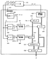
図1は、本発明に係る位置検出装置を曲線(部分的回転)型の位置検出器として構成した例を示す。固定されたコイル部10は、所定距離離隔された第1及び第2の位置においてそれぞれ配置された第1の2次コイル2cと、第2の2次コイル2sと、その中間に配置された1次コイル1pとを含む。回転軸(若しくは揺動軸)3に扇型の可動部4が設けられており、この可動部4における円弧寄りの位置に磁気応答部材5が設けられており、各コイルに非接触的に対応している。公知のように、磁気応答部材5は、磁性体又は導電体のどちらを用いてもよく、また、両者を適宜組み合わせたハイブリッド構造でもよい。磁性体の場合は、磁気応答部材5のコイルへの近接に応じてパーミアンスが増加し、誘導レベルが上がる。反対に導電体の場合は、磁気応答部材のコイルへの近接に応じて渦電流損が生じ、誘導レベルが下がる。以下では、磁気応答部材5が磁性体であるとして説明する。また、可動部4の全体が磁気応答部材5であってもよい。
【0019】
1次コイル1pは、所定の1相の交流信号(例えば便宜sinωtとする)によって励磁され、その磁界を各2次コイルに及ぼす。磁気応答部材5の幅は、一方の2次コイル2cと1次コイル1pとをカバーする程度の大きさであり、1次コイル1pからの磁気が磁気応答部材5を通って2次コイル2c又は2sに流れる。各コイルは、磁気の通りをよくするために鉄心コアに巻回されてなる構成であるのがよい。
2次コイル2cと2sの間隔は、例えば、可動部4の回動角度にして90度位に対応するものであってよいが、これに限らず、それ以上であってもよいし、それ以下であってもよい。なお、磁気応答部材5が一方の2次コイル2cに最も接近しているときは、他方の2次コイル2sには磁気応答部材5が全く近づいておらず、逆に磁気応答部材5が他方の2次コイル2sに最も接近しているときは、一方の2次コイル2cには磁気応答部材5が全く近づいていない、というような関係である。これにより、磁気応答部材5の相対的変位に応じた異なる誘導出力信号が各2次コイル2c,2sから出力される。
【0020】
磁気応答部材5が第1の2次コイル2cに最も近接して該第1の2次コイル2cに最大レベル(例えば1)の誘導を生じさせるとき、別の位置に在る第2の2次コイル2sには最小レベル(例えば0)の誘導しか生じない。この状態を例えば角度θで示し、θ=0度とすると、第1の2次コイル2cの出力レベルはcosθに相当し、第2の2次コイル2sの出力レベルはsinθに相当すると、考えることができる。
逆に、磁気応答部材5が第2の2次コイル2sに最も近接して該第2の2次コイルに最大レベル(例えば1)の誘導を生じさせるとき、第1の2次コイル2cには最小レベル(例えば0)の誘導しか生じない。すなわち、sinθ=1,cosθ=0であるから、θ=90度に相当する。
【0021】
このように、第1の2次コイル2cに最接近する位置から第2の2次コイル2sに最接近する位置までの間の磁気応答部材5の変位は、角度θにして、0度から90度までの変位に換算して表現することができる。
従って、この範囲での磁気応答部材5の変位に対応して第1の2次コイル2cに生じる誘導出力信号は、見掛け上、
「cosθ・sinωt」と表わせる。ただし、θは0度〜90度であり、sinωtは交流成分である。
同様に、磁気応答部材5の変位に対応して第2の2次コイル2sに生じる誘導出力信号は、見掛け上、
「sinθ・sinωt」と表わせる。ただし、θは0度〜90度である。
【0022】
第2の2次コイル2sの出力(sinθ・sinωt)が位相シフト回路6に入力され、その電気的位相が略90度ずらされ、
「sinθ・cosωt」
に変換される。
そして、回路7において、位相シフト回路6の出力と第1の2次コイル2cの出力とが合成(例えば加算合成;あるいは減算合成でもよい)され、概算的に示して、
cosθ・sinωt+sinθ・cosωt=sin(ωt+θ)
という出力交流信号を得る。こうして、磁気応答部材5の相対的変位位置に応じた電気的位相角θを示す出力交流信号を得ることができる。ただし、θはほぼ0度〜90度の範囲に限定される。
【0023】
この回路7の出力を、適当な位相測定回路8に入力すれば、その電気的位相角θを、デジタル的に若しくはアナログ的に測定することができる。位相測定回路8は、公知のパルスカウント方式又はアナログ電圧積分方式等などによって適宜構成してよい。
なお、可動部4の回動角度φの絶対値と、それに対応して検出される上記電気的位相角θの絶対値とは必ずしも一致しない。しかし、概ね、2次コイル2c,2sの配置間隔がほぼ90度であれば略一致する。要するに、2次コイル2c,2sの配置間隔が、電気的位相角θにして略90度の幅に対応している。
【0024】
図2は、上記の関係をベクトル図で示したものである。X軸がcosθすなわち第1の2次コイル2cの出力レベル、Y軸がsinθすなわち第2の2次コイル2sの出力レベル、である。X値とY値をベクトル合成したベクトルの角度がθである。
なお、1次コイル1pは、各2次コイル2c,2sと同じ位置にそれぞれ分けて設けてもよい。
上記の場合、可動部4の回動検出範囲を検出可能範囲の限界ぎりぎりに設定すると、その範囲の両端では精度が落ちるため、中ほどの範囲で位置検出を行うように設計するとよい。
【0025】
図3は、図1の位置検出装置を改良した実施例を示し、検出分解能を向上させると共に、検出可能範囲の限界ぎりぎりの使用でも或る程度精度が出せるようにしたものである。
図1の相違について説明すると、上記第1及び第2の2次コイル2c,2sが主2次コイルとして機能し、それぞれと同じ位置に、それよりも巻数の少ない(誘導係数の小さい)副2次コイル2s’と2c’を設けている。つまり、第1の2次コイル2cの位置に第1の副2次コイル2s’を配置し、第2の2次コイル2sの位置に第2の副2次コイル2c’を配置する。
第1の主2次コイル2cに対して、第2の副2次コイル2c’が逆相のインダクタンス変化を示すとすると、第2の副2次コイル2c’の出力レベルは、−cosθで表わせるが、誘導係数を小さくしてあるため、真の逆相ではないので、便宜上、これを−cosθ’で示すこととする。
同様に、第2の主2次コイル2sに対する第1の副2次コイル2s’の出力レベルを、−sinθ’で示すこととする。
【0026】
第1の主2次コイル2cの誘導出力信号cosθ・sinωt(これをCsinωtで示す)と、第2の副2次コイル2c’の誘導出力信号−cosθ’・sinωt(これを−C’sinωtで示す)とを、回路11で差動合成し、レベル増加された出力「(C+C’)sinωt」を得る。
また、第2の主2次コイル2sの誘導出力信号sinθ・sinωt(これをSsinωtで示す)と、第1の副2次コイル2s’の誘導出力信号−sinθ’・sinωt(これを−S’sinωtで示す)とを、回路9で差動合成し、レベル増加された出力「(S+S’)sinωt」を得る。そして、この回路9の出力を位相シフト回路6に入力し、その電気的位相を略90度ずらし、
「(S+S’)cosωt」
を得る。
そして、回路7において、位相シフト回路6の出力と回路11の出力とを合成(例えば加算合成;あるいは減算合成でもよい)し、概算的に示して、
(C+C’)sinωt+(S+S’)cosωt=sin(ωt+θ)
という出力交流信号を得る。こうして、磁気応答部材5の相対的変位位置に応じた電気的位相角θを示す出力交流信号を得ることができる。ただし、θは0度〜90度の範囲よりもその前後にいくらか拡大される。従って、検出分解能を向上させると共に、検出可能範囲の限界ぎりぎりの使用でも或る程度精度が出せるようになる。
【0027】
この点について説明すると、主2次コイルの誘導係数よりも副2次コイルの誘導係数を小さく設定していることがポイントである。これにより、見掛上の角変換を行うことができる。例えば、副2次コイルのコイル巻数を、主2次コイルのコイル巻数の半分に設定することにより、その誘導係数を小さくする例を考えてみる。そうすると、第2の主2次コイル2sの位置における本来の相は上記のようにsinθであるから、第2の副2次コイル2c’の誘導出力レベル−cosθ’はこれに90度遅れているところ、コサイン相の1/2のインダクタンス減少によって見掛け上60度進相となり(cos60度=1/2)、sinθよりも約30度だけ遅れたマイナスコサイン成分に相当する誘導が該第2の副2次コイル2c’に生じることになる。
同様に、第1の副2次コイル2s’において見掛け上30度進相(sin30度=1/2)のマイナスサイン成分に相当する誘導出力レベル−sinθ’が生じる。
【0028】
これによって、第1及び第2の主2次コイル2c,2s間の磁気応答部材5の変位に対応する電気的位相角θの変化範囲は、図1の例における0度から90度までの範囲に比べて、約±30度拡大されて、−30度から約+120度の範囲となる。従って、この電気的位相角θを測定して位置検出データを得る場合に、検出分解能を向上させることができることとなる。この拡大幅は、主2次コイルと副2次コイルの誘導係数の比率に応じて変化させることができる。
これをベクトル図によって示すと図4のようである。第4象限のベクトル12が、第1の主2次コイル2c及び第2の副2次コイル2c’に磁気応答部材5が最接近しているときの角度θのベクトル、第2象限のベクトル13が、第2の主2次コイル2s及び第1の副2次コイル2s’に磁気応答部材5が最接近しているときの角度θのベクトル、を示す。
【0029】
なお、図3に示したような主コイルと副コイルを同一位置に設ける発想は、電気的位相を測定するタイプの位置検出装置に限らず、振幅電圧レベルを測定するタイプにも適用することができる。すなわち、回路11により記第1の主2次コイルと第2の副2次コイルの誘導出力信号を差動合成して第1の出力交流信号(C+C’)sinωtを取り出し、また、回路9により前記第2の主2次コイルと第1の副2次コイルの誘導出力信号を差動合成して第2の出力交流信号(S+S’)sinωtを取り出す。そして、両出力交流信号をそれぞれ整流して振幅レベル電圧C+C’及びS+S’を得て、両振幅レベル電圧の比又は差に基づき、少なくとも前記第1及び第2の位置間における前記磁気応答部材の相対的変位位置を検出するようにすることができる。この場合も、測定分解能を向上させることができ、簡易なアナログ出力電圧の形で、かつ、測定精度が相対的に向上された位置検出出力を得る場合に適している。
【0030】
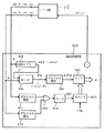
また、上記のような主コイルと副コイルを同一位置に設ける発想は、図5に示すように、2相の交流信号(例えばsinωtとcosωt)で励磁する位相シフトタイプ誘導型位置検出装置にも適用できる。
図5は、1次コイルと2次コイルの関係を図3とは逆にし、中央のコイル1Pが2次コイル、他が1次コイルとなっている。すなわち、第1の主1次コイル2cを所定の交流信号cosωtで励磁し、それと同じ位置に在る第1の副1次コイル2s’をそれよりも90度位相のずれた交流信号−sinωtで励磁する。また、第2の主1次コイル2sを−sinωtと逆相の交流信号sinωtで励磁し、それと同じ位置に在る第2の副1次コイル2c’をcosωtと逆相の交流信号−cosωtで励磁する。各1次コイルによる誘導電圧の合成により、位相シフトが生じ、磁気応答部材5の相対的変位位置に応じた電気的位相角θを示す出力交流信号が2次コイル1pから得られる。
この場合も、従来装置に比べて、上記と同様の効果を得ることができる。また、このような位相シフトタイプの場合も、上記と同様に各主1次コイル2c,2sの誘導係数より各副1次コイル2c’,2s’の誘導係数を小さくするようにしてよい。
【0031】
上記各例のように、磁気応答部材5が、所定の角度範囲内で円弧状の軌跡で往復動するような形態からなる位置検出装置は、軸3の僅かな動きを精度よく、しかも、簡易な構成で、検出するのに適しており、様々な分野での新規な位置検出装置として利用することができる。
【0032】
図6は、本発明の2極型位置センサの一実施例を示す略図である。この2極型位置センサ300は直線位置検出装置として構成されており、サイン相とコサイン相に相当する2極分の2次コイル302S,302Cを設けたものである。その分だけ、位置に応じて検出できる位相ずれ成分θの範囲は、360度全部で現われず、略90度以内の範囲に限定される。しかし、比較的狭い範囲での直線位置又は角度θの振れ又は傾きを検出する等の限られた用途によっては、これで十分であり、そのような用途においてそ、簡易な2極型位置センサとして応用することができる。
【0033】
この2極型位置センサ300は、1相の交流信号によって励磁される少なくとも1つの1次コイル301及び該1次コイルの近傍において互いに所定距離離隔して配置された第1及び第2の2次コイル302S,302Cとを含むコイル部と、検出対象たる直線的な又は曲線的な変位に応答して前記コイル部に対して相対的に変位される磁気応答部材303であって、この磁気応答部材303の前記コイル部に対する相対的変位に応じた誘導出力信号が前記2つの2次コイル302S,302Cから夫々出力されるようにしたものとを具備する。更に、各2次コイル302S,302Cからの前記誘導出力信号の振幅関数の位相ずれ成分θを測定するための手段を適宜設ける。
検出対象たる直線変位は、可動部304に伝達される。可動部304の所定位置には磁気応答部材303が設けられていて、検出対象たる直線変位に応じて磁気応答部材303が変位する。
図7(a),(b),(c)は、上記直線型の2極型位置センサ300における1次及び2次コイル301,302S,302Cの配置のバリエーションを示す。
【0034】
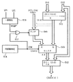
図8は、本発明に係る位置検出装置に適用される新規なディジタル位相検出回路40の一実施形態を示している。
図8において、検出回路部41では、カウンタ42で所定の高速クロックパルスCKをカウントし、そのカウント値に基づき励磁信号発生回路43から励磁用の交流信号(例えばsinωt)を発生し、コイル部10の1次コイル2a(又は11〜14)に与える。カウンタ42のモジュロ数(進数)は、励磁用の交流信号の1周期に対応しており、説明の便宜上、そのカウント値の0は、基準のサイン信号sinωtの0位相に対応しているものとする。コイル部10の2次コイル2b(又は21〜24)から出力される2相の出力交流信号A=sinθ・sinωtとB=cosθ・sinωtは、検出回路部41に入力される。
【0035】
検出回路部41において、第1の交流出力信号A=sinθ・sinωtが位相シフト回路44に入力され、その電気的位相が所定量位相シフトされ、例えば90度進められて、位相シフトされた交流信号A’=sinθ・cosωtが得られる。また、検出回路部41においては加算回路45と減算回路46とが設けられており、加算回路45では、位相シフト回路44から出力される上記位相シフトされた交流信号A’=sinθ・cosωtとコイル部10の2次コイルから出力され第2の交流出力信号B=cosθ・sinωtとが加算され、その加算出力として、B+A’=cosθ・sinωt+sinθ・cosωt=sin(ωt+θ)なる略式で表わせる第1の電気的交流信号Y1が得られる。減算回路46では、上記位相シフトされた交流信号A’=sinθ・cosωtと上記第2の交流出力信号B=cosθ・sinωtとが減算され、その減算出力として、B−A’=cosθ・sinωt−sinθ・cosωt=sin(ωt−θ)なる略式で表わせる第2の電気的交流信号Y2が得られる。このようにして、検出対象角θに対応して正方向にシフトされた電気的位相角(+θ)を持つ第1の電気的交流信号Y1=sin(ωt+θ)と、同じ前記検出対象位置(x)に対応して負方向にシフトされた電気的位相角(−θ)を持つ第2の電気的交流信号Y2=sin(ωt−θ)とが、電気的処理によって夫々得られる。
【0036】
加算回路45及び減算回路46の出力信号Y1,Y2は、夫々ゼロクロス検出回路47,48に入力され、それぞれのゼロクロスが検出される。ゼロクロスの検出の仕方としては、例えば、各信号Y1,Y2の振幅値が負から正に変化するゼロクロスつまり0位相を検出する。各回路47,48で検出したゼロクロス検出パルスつまり0位相検出パルスは、ラッチパルスLP1,LP2として、ラッチ回路49,50に入力される。ラッチ回路49,50では、カウンタ42のカウント値を夫々のラッチパルスLP1,LP2のタイミングでラッチする。前述のように、カウンタ42のモジュロ数(進数)は励磁用の交流信号の1周期に対応しており、そのカウント値の0は基準のサイン信号sinωtの0位相に対応しているものとしたので、各ラッチ回路49,50にラッチしたデータD1,D2は、それぞれ、基準のサイン信号sinωtに対する各出力信号Y1,Y2の位相ずれに対応している。各ラッチ回路49,50の出力は誤差計算回路51に入力されて、「(D1+D2)/2」の計算が行なわれる。なお、この計算は、実際は、「D1+D2」のバイナリデータの加算結果を1ビット下位にシフトすることで行われるようになっていてよい。
【0037】
ここで、コイル部10と検出回路部41間の配線ケーブル長の長短による影響や、コイル部10の各1次及び2次コイルにおいて温度変化等によるインピーダンス変化が生じていることを考慮して、その出力信号の位相変動誤差を「±d」で示すと、検出回路部41における上記各信号は次のように表わされる。
A=sinθ・sin(ωt±d)
A’=sinθ・cos(ωt±d)
B=cosθ・sin(ωt±d)
Y1=sin(ωt±d+θ)
Y2=sin(ωt±d−θ)
D1=±d+θ
D2=±d−θ
【0038】
すなわち、各位相ずれ測定データD1,D2は、基準のサイン信号sinωtを基準位相に使用して位相ずれカウントを行なうので、上記のように位相変動誤差「±d」を含む値が得られてしまう。そこで、誤差計算回路51において、「(D1+D2)/2」の計算を行なうことにより、

【0039】
誤差計算回路51で求められた位相変動誤差「±d」のデータは、減算回路52に与えられ、一方の位相ずれ測定データD1から減算される。すなわち、減算回路52では、「D1−(±d)」の減算が行なわれるので、
D1−(±d)=±d+θ−(±d)=θ
となり、位相変動誤差「±d」を除去した正しい検出位相差θを示すディジタルデータが得られる。このように、本発明によれば、位相変動誤差「±d」が相殺されて、検出対象量θに対応する正しい位相差θのみが抽出されることが理解できる。
【0040】
この点を図9を用いて更に説明する。図9においては、位相測定の基準となるサイン信号sinωtと前記第1及び第2の交流信号Y1,Y2の0位相付近の波形を示しており、同図(a)は位相変動誤差がプラス(+d)の場合、(b)はマイナスの場合(−d)を示す。同図(a)の場合、基準のサイン信号sinωtの0位相に対して第1の信号Y1の0位相は「θ+d」だけ進んでおり、これに対応する位相差検出データD1は「θ+d」に相当する位相差を示す。また、基準のサイン信号sinωtの0位相に対して第2の信号Y2の0位相は「−θ+d」だけ遅れており、これに対応する位相差検出データD2は「−θ+d」に相当する位相差を示す。この場合、誤差計算回路51では、
D1−(+d)=+d+θ−(+d)=θ
が計算され、正しい位相差θが抽出される。
【0041】
図9(b)の場合、基準のサイン信号sinωtの0位相に対して第1の信号Y1の0位相は「θ−d」だけ進んでおり、これに対応する位相差検出データD1は「θ−d」に相当する位相差を示す。また、基準のサイン信号sinωtの0位相に対して第2の信号Y2の0位相は「−θ−d」だけ遅れており、これに対応する位相差検出データD2は「−θ−d」に相当する位相差を示す。この場合、誤差計算回路51では、
D1−(−d)=−d+θ−(−d)=θ
が計算され、正しい位相差θが抽出される。
なお、減算回路52では。「D2−(±d)」の減算を行なうようにしてもよく、原理的には上記と同様に正しい位相差θを反映するデータ(−θ)が得られることが理解できるであろう。
【0042】
また、図9からも理解できるように、第1の信号Y1と第2の信号Y2との間の電気的位相差は2θであり、常に、両者における位相変動誤差「±d」を相殺した正確な位相差θの2倍値を示していることになる。従って、図8におけるラッチ回路49,50及び誤差計算回路51及び減算回路52等を含む回路部分の構成を、信号Y1,Y2の電気的位相差2θをダイレクトに求めるための構成に適宜変更するようにしてもよい。例えば、ゼロクロス検出回路47から出力される第1の信号Y1の0位相に対応するパルスLP1の発生時点から、ゼロクロス検出回路48から出力される第2の信号Y2の0位相に対応するパルスLP2の発生時点までの間を適宜の手段でゲートし、このゲート期間をカウントすることにより、位相変動誤差「±d」を相殺した、電気的位相差(2θ)に対応するディジタルデータを得ることができ、これを1ビット下位にシフトすれば、θに対応するデータが得られる。
【0043】
ところで、上記実施例では、+θをラッチするためのラッチ回路49と、−θをラッチするためのラッチ回路50とでは、同じカウンタ42の出力をラッチするようにしており、ラッチしたデータの正負符号については特に言及していない。しかし、データの正負符号については、本発明の趣旨に沿うように、適宜の設計的処理を施せばよい。例えば、カウンタ42のモジュロ数(進数)が4096(10進数表示)であるとすると、そのディジタルカウント0〜4095を0度〜360度の位相角度に対応させて適宜に演算処理を行なうようにすればよい。最も単純な設計例は、カウンタ42のカウント出力の最上位ビットを符号ビットとし、ディジタルカウント0〜2047を+0度〜+180度に対応させ、ディジタルカウント2048〜4095を−180度〜−0度に対応させて、演算処理を行なうようにしてもよい。あるいは、別の例として、ラッチ回路50の入力データ又は出力データを2の補数に変換することにより、ディジタルカウント4095〜0を−360度〜−0度の負の角度データ表現に対応させるようにしてもよい。
【0044】
ところで、が静止状態のときは特に問題ないのであるが、検出対象量θが時間的に変化するときは、それに対応する位相角θも時間的に変動することになる。その場合、加算回路45及び減算回路46の各出力信号Y1,Y2の位相ずれ量θが一定値ではなく、移動速度に対応して時間的に変化する動特性を示すものとなり、これをθ(t)で示すと、各出力信号Y1,Y2は、
Y1=sin{ωt±d+θ(t)}
Y2=sin{ωt±d−θ(t)}
となる。すなわち、基準信号sinωtの周波数に対して、進相の出力信号Y1は+θ(t)に応じて周波数が高くなる方向に周波数遷移し、遅相の出力信号Y2は−θ(t)に応じて周波数が低くなる方向に周波数遷移する。このような動特性の下においては、基準信号sinωtの1周期毎に各信号Y1,Y2の周期が互いに逆方向に次々に遷移していくので、各ラッチ回路49,50における各ラッチデータD1,D2の計測時間基準が異なってくることになり、両データD1,D2を単純に回路51,52で演算するだけでは、正確な位相変動誤差「±d」を得ることができない。
【0045】
このような問題を回避するための最も簡単な方法は、図8の構成において、量θが時間的に動いているときの出力を無視し、静止状態のときの出力のみを用いて、静止状態が得られた時の量θを測定するように装置の機能を限定することである。すなわち、そのような限定された目的のために本発明を実施するようにしてもよいものである。また、振動の最大振幅のときの量θを検出することのみで足りる場合も、最大振幅時の検出値をピークホールドするような処理の仕方で対処できる。
一方、検出対象量θが時間的に変化している最中であっても時々刻々の該検出対象量θに対応する位相差θを正確に検出できるようにしたい、という要求もアプリケーションの場面によってはあり得る。そこで、検出対象が時間的に変化している最中であっても時々刻々の該検出対象量θに対応する位相差θを検出できるようにした改善策について図10を参照して説明する。
【0046】
図10は、図8の検出回路部41における誤差計算回路51と減算回路52の部分の変更例を抽出して示しており、他の図示していない部分の構成は図8と同様であってよい。検出対象量θが時間的に変化している場合における該量θに対応する位相差θを、+θ(t)および−θ(t)で表わすと、各出力信号Y1,Y2は前記のように表わせる。そして、夫々に対応してラッチ回路49,50で得られる位相ずれ測定値データD1,D2は、
D1=±d+θ(t)
D2=±d−θ(t)
となる。
この場合、±d+θ(t) は、θの時間的変化に応じて、プラス方向に0度から360度の範囲で繰り返し時間的に変化してゆく。また、±d−θ(t) は、θの時間的変化に応じて、マイナス方向に360度から0度の範囲で繰り返し時間的に変化してゆく。従って、±d+θ(t) ≠ ±d−θ(t) のときもあるが、両者の変化が交差するときもあり、そのときは±d+θ(t) = ±d−θ(t) が成立する。このように、±d+θ(t) = ±d−θ(t) が成立するときは、各出力信号Y1,Y2の電気的位相が一致しており、かつ、夫々のゼロクロス検出タイミングに対応するラッチパルスLP1,LP2の発生タイミングが一致していることになる。
【0047】
図10において、一致検出回路53は、各出力信号Y1,Y2ののゼロクロス検出タイミングに対応するラッチパルスLP1,LP2の発生タイミングが、一致したことを検出し、この検出に応答して一致検出パルスEQPを発生する。一方、時変動判定回路54では、適宜の手段により(例えば一方の位相差測定データD1の値の時間的変化の有無を検出する等の手段により)、検出対象角θが時間的に変化するモードであることを判定し、この判定に応じて時変動モード信号TMを出力する。
誤差計算回路51と減算回路52との間にセレクタ55が設けられており、上記時変動モード信号TMが発生されていないとき、つまりTM=“0”すなわち検出対象角θが時間的に変化していないとき、セレクタ入力Bに加わる誤差計算回路51の出力を選択して減算回路52に入力する。このようにセレクタ55の入力Bが選択されているときの図10の回路は、図8の回路と等価的に動作する。すなわち、検出対象角θが静止しているときは、誤差計算回路51の出力データがセレクタ55の入力Bを介して減算回路52に直接的に与えられ、図8の回路と同様に動作する。
【0048】
一方、上記時変動モード信号TMが発生されているとき、つまりTM=“1”すなわち検出対象角θが時間的に変化しているときは、セレクタ55の入力Aに加わるラッチ回路56の出力を選択して減算回路52に入力する。上記時変動モード信号TMが“1”で、かつ前記一致検出パルスEQPが発生されたとき、アンドゲート57の条件が成立して、該一致検出パルスEQPに応答するパルスがアンドゲート57から出力され、ラッチ回路56に対してラッチ命令を与える。ラッチ回路56は、このラッチ命令に応じてカウンタ42の出力カウントデータをラッチする。ここで、一致検出パルスEQPが生じるときは、カウンタ42の出力をラッチ回路49,50に同時にラッチすることになるので、D1=D2であり、ラッチ回路56にラッチするデータは、D1又はD2(ただしD1=D2)に相当している。
【0049】
また、一致検出パルスEQPは、各出力信号Y1,Y2のゼロクロス検出タイミングが一致したとき、すなわち「±d+θ(t) = ±d−θ(t)」が成立したとき、発生されるので、これに応答してラッチ回路56にラッチされるデータは、D1又はD2(ただしD1=D2)に相当しているが故に、
(D1+D2)/2
と等価である。このことは、
【0050】
こうして、検出対象量θが時間的に変動しているときは、位相変動誤差「±d」を正確に示すデータが一致検出パルスEQPに応じてラッチ回路56にラッチされ、このラッチ回路56の出力データがセレクタ55の入力Aを介して減算回路52に与えられる。従って、減算回路52では、位相変動誤差「±d」を除去した検出対象量θのみに正確に応答するデータθ(時間的に変動する場合はθ(t) )を得ることができる。
なお、図10において、アンドゲート57を省略して、一致検出パルスEQPを直接的にラッチ回路56のラッチ制御入力に与えるようにしてもよい。
また、ラッチ回路56には、カウンタ42の出力カウントデータに限らず、図10で破線で示すように誤差計算回路51の出力データ「±d」をラッチするようにしてもよい。その場合は、一致検出パルスEQPの発生タイミングに対して、それに対応する誤差計算回路51の出力データの出力タイミングが、ラッチ回路49,50及び誤差計算回路51の回路動作遅れの故に、幾分遅れるので、適宜の時間遅れ調整を行なった上で、誤差計算回路51の出力をラッチ回路56にラッチするようにするとよい。
また、動特性のみを考慮して検出回路部41を構成する場合は、図10の回路51及びセレクタ55と図8の一方のラッチ回路49又は50を省略してもよいことが、理解できるであろう。
【0051】
図11は、位相変動誤差「±d」を相殺することができる位相差検出演算法についての別の実施例を示す。
コイル部10の2次コイル21〜24から出力されるレゾルバタイプの前記第1及び第2の交流出力信号A,Bは、検出回路部60に入力され、図8の例と同様に、第1の交流出力信号A=sinθ・sinωtが位相シフト回路44に入力され、その電気的位相が所定量位相シフトされて、位相シフトされた交流信号A’=sinθ・cosωtが得られる。また、減算回路46では、上記位相シフトされた交流信号A’=sinθ・cosωtと上記第2の交流出力信号B=cosθ・sinωtとが減算され、その減算出力として、B−A’=cosθ・sinωt−sinθ・cosωt=sin(ωt−θ)なる略式で表わせる電気的交流信号Y2が得られる。減算回路46の出力信号Y2はゼロクロス検出回路48に入力され、ゼロクロス検出に応じてラッチパルスLP2が出力され、ラッチ回路50に入力される。
【0052】
図11の実施例が図8の実施例と異なる点は、検出対象に対応する電気的位相ずれを含む交流信号Y2=sin(ωt−θ)から、その位相ずれ量θを測定する際の基準位相が相違している点である。図8の例では、位相ずれ量θを測定する際の基準位相は、基準のサイン信号sinωtの0位相であり、これは、検出装置10のコイル部10に入力されるものではないので、温度変化等によるコイルインピーダンス変化やその他の各種要因に基づく位相変動誤差「±d」を含んでいないものである。そのために、図8の例では、2つの交流信号Y1=sin(ωt+θ)及びY2=sin(ωt−θ)を形成し、その電気的位相差を求めることにより、位相変動誤差「±d」を相殺するようにしている。これに対して、図11の実施例では、コイル部10から出力される第1及び第2の交流出力信号A,Bを基にして、位相ずれ量θを測定する際の基準位相を形成し、該基準位相そのものが上記位相変動誤差「±d」を含むようにすることにより、上記位相変動誤差「±d」を排除するようにしている。
【0053】
すなわち、検出回路部60において、コイル部10から出力された前記第1及び第2の交流出力信号A,Bがゼロクロス検出回路61,62に夫々入力され、それぞれのゼロクロスが検出される。なお、ゼロクロス検出回路61,62は、入力信号A,Bの振幅値が負から正に変化するゼロクロス(いわば0位相)と正から負に変化するゼロクロス(いわば180度位相)のどちらにでも応答してゼロクロス検出パルスを出力するものとする。これは信号A,Bの振幅の正負極性を決定するsinθとcosθがθの値に応じて任意に正又は負となるため、両者の合成に基づき360度毎のゼロクロスを検出するためには、まず180度毎のゼロクロスを検出する必要があるためである。両ゼロクロス検出回路61,62から出力されるゼロクロス検出パルスがオア回路63でオア合成され、該オア回路63の出力が適宜の1/2分周パルス回路64(例えばT−フリップフロップのような1/2分周回路とパルス出力用アンドゲートを含む)に入力されて、1つおきに該ゼロクロス検出パルスが取り出され、360度毎のゼロクロスすなわち0位相のみに対応するゼロクロス検出パルスが基準位相信号パルスRPとして出力される。この基準位相信号パルスRPは、カウンタ65のリセット入力に与えられる。カウンタ65は所定のクロックパルスCKを絶えずカウントするものであるが、そのカウント値が、前記基準位相信号パルスRPに応じて繰返し0にリセットされる。このカウンタ65の出力がラッチ回路50に入力され、前記ラッチパルスLP2の発生タイミングで、該カウント値が該ラッチ回路50にラッチされる。ラッチ回路50にラッチしたデータDが、検出対象量θに対応した位相差θの測定データとして出力される。
【0054】
コイル部10から出力される第1及び第2の交流出力信号A,Bは、それぞれ、A=sinθ・sinωt、B=cosθ・sinωt、であり、電気的位相は同相である。従って、同じタイミングでゼロクロスが検出されるはずであるが、振幅係数がサイン関数sinθ及びコサイン関数cosθで変動するので、どちらかの振幅レベルが0か又は0に近くなる場合があり、そのような場合は、一方については、事実上、ゼロクロスを検出することができない。そこで、この実施例では、2つの交流出力信号A=sinθ・sinωt、B=cosθ・sinωtのそれぞれについてゼロクロス検出処理を行ない、両者のゼロクロス検出出力をオア合成することにより、どちらか一方が振幅レベル小によってゼロクロス検出不能であっても、他方の振幅レベル大の方のゼロクロス検出出力信号を利用できるようにしたことを特徴としている。
【0055】
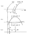
図11の例の場合、コイル部10のコイルインピーダンス変化等による位相変動誤差が、例えば「−d」であるとすると、減算回路46から出力される交流信号Y2は、図12の(a)に示すように、Y2=sin(ωt−d−θ)となる。この場合、コイル部10の出力信号A,Bは、角度θに応じた振幅値sinθ及びcosθを夫々持ち、図12の(b)に例示するように、A=sinθ・sin(ωt−d)、B=cosθ・sin(ωt−d)、というように位相変動誤差分を含んでいる。従って、このゼロクロス検出に基づいて図12の(c)のようなタイミングで得られる基準位相信号パルスRPは、本来の基準のサイン信号sinωtの0位相から位相変動誤差−dだけずれたものである。従って、この基準位相信号パルスRPを基準として、減算回路46の出力交流信号Y2=sin(ωt−d−θ)の位相ずれ量を測定すれば、位相変動誤差−dを除去した正確な値θが得られることになる。
【0056】
【発明の効果】
以上の通り、本発明によれば、2次コイル又は1次コイルの極配置を基本的に2極構造として、小型かつシンプルな構造により、必要な範囲での位置検出を可能にした誘導型位置検出装置を提供することができる。また、所定の比較的狭い角度範囲で往復動する検出対象の位置を、小型かつシンプルな構造により、検出しうるようにした誘導型位置検出装置を提供することができる。
【図面の簡単な説明】
【図1】 本発明の一実施例を示す図
【図2】 図1の動作を示すベクトル図
【図3】 本発明の別の実施例を示す図
【図4】 図3の動作を示すベクトル図
【図5】 本発明の更に別の実施例を示す図
【図6】 本発明の更に他の実施例を示す図
【図7】 図6の変形例を示す図
【図8】 本発明に係る検出装置に適用可能な位相検出タイプの測定回路の一例を示すブロック図。
【図9】 図8の動作説明図。
【図10】 図9の回路に付加される変更例を示すブロック図。
【図11】 本発明に係る検出装置に適用可能な位相検出タイプの測定回路の更に別の例を示すブロック図。
【図12】 図11の動作説明図。
【符号の説明】
10 コイル部
1p 1次コイル
2c,2s 2次コイル
3 回転軸
4 可動部
5 磁気応答部材[0001]
BACKGROUND OF THE INVENTION
The present invention relates to an inductive position detection device having a two-pole structure in which a secondary coil that generates an induction output or a primary coil for excitation is arranged.
[0002]
[Prior art]
As a conventionally known inductive linear position detecting device, there is a differential transformer. The differential transformer excites one primary winding in one phase, and differentially varies according to the linear position of the iron core that is linked to the detection target position at each of the two secondary windings that are differentially connected. The reluctance which changes continuously is produced, and the voltage amplitude level of the one-phase induction output AC signal obtained as a result indicates the linear position of the iron core. In this differential transformer, in the range in which two secondary windings are provided so that the induced voltage changes in a differential manner, the induced voltage value is only in a range showing linearity with respect to the straight line position. The linear position cannot be detected, and the function of the change in the induced voltage value versus the linear position does not change over one cycle of a periodic function (for example, a trigonometric function such as a sine function). Accordingly, in order to extend the detectable range, the winding length and the core length must be increased, which naturally has limitations and increases the size of the apparatus. Further, it is impossible to obtain an output indicating an electrical phase correlated with the detection target linear position. Further, the voltage amplitude level of the induction output signal is susceptible to the influence of not only the linear position of the iron core but also the surrounding environment such as a temperature change, and thus there is a problem in accuracy.
[0003]
On the other hand, a phase shift type inductive linear position detection device that outputs an alternating current signal having an electrical phase angle correlated with a detection target linear position is also known. For example, there are those disclosed in JP-A-49-107758, JP-A-53-106065, JP-A-55-13891, JP-A-1-25286, and the like. In this type of conventionally known phase type induction type linear position detecting device, for example, two primary windings arranged so as to be shifted from each other with respect to the linear displacement direction of the movable core core linked to the detection target position are electrically connected to each other. Excitation is performed with two-phase AC signals (for example, sin ωt and cos ωt) that are out of phase, and the secondary induction signals from the primary windings are combined to generate one secondary output signal. . The electrical phase shift in the secondary output signal with respect to the excitation AC signal indicates the linear position of the iron core that is linked to the detection target position. Moreover, in what is shown in Japanese Utility Model Publication No. 1-25286, a plurality of iron cores are intermittently repeatedly provided at a predetermined pitch, and linear position detection over a wider range than the range in which primary and secondary windings are provided. Is possible.
[0004]
The above-described conventional phase shift type inductive linear position detector has advantages in many respects as compared with the differential transformer, but also has drawbacks. For example, since at least two-phase excitation AC signals (for example, sin ωt and cos ωt) must be prepared, there is a problem that the configuration of the excitation circuit becomes complicated. In addition, when the impedances of the primary and secondary windings change due to a temperature change or the like, there is a drawback that an error occurs in the electrical phase shift in the secondary output signal. In addition, when a plurality of iron cores are intermittently repeatedly provided at a predetermined pitch to enable linear position detection over a wider range than the range where the primary and secondary windings are provided, the primary and secondary windings Therefore, the entire winding assembly is increased in size, and there is a limit to downsizing of the detection apparatus. That is, if the length of one pitch of the iron core is P, in the case of the four-phase type, the arrangement interval of the windings of each phase must be “3P / 4” at the minimum, and the total of “4” is four times that X (3P / 4) = 3P "is required, so the winding assembly must be provided over a range of at least three pitch lengths of the movable core.
[0005]
[Problems to be solved by the invention]
In the conventional phase shift type inductive position detecting device, coils having different output phases such as a sine phase and a cosine phase must be provided in different pole arrangements. For example, in the case of a four-phase type, at least a 4-pole type coil arrangement configuration is always used. Therefore, there is a limit to downsizing the configuration of the position detection device.
In addition, not only the phase shift type but also the conventional inductive position detection device including a resolver etc., as a basic principle, the coils are arranged in a plurality of pole arrangements so as to obtain a phase change of at least one cycle. Yes. Therefore, even when the position detection device is used only for position detection in a relatively narrow range, the number of poles of the coil cannot be reduced, and resource utilization efficiency is poor.
The present invention has been made in view of the above-mentioned points. The pole arrangement of the secondary coil or the primary coil is basically a two-pole structure, and a small and simple structure enables position detection within a necessary range. It is an object of the present invention to provide an inductive position detecting apparatus.
It is another object of the present invention to provide an inductive position detection device that can detect the position of a detection object that reciprocates within a predetermined relatively narrow angle range with a small and simple structure.
[0006]
[Means for Solving the Problems]
An inductive position detecting device according to the present invention includes first and second poles configured by coils respectively excited at a first and second positions that are excited by a predetermined alternating current signal and separated by a predetermined distance. A magnetic response member that is displaced relative to the coil portion in response to a linear or curvilinear displacement to be detected, the relative displacement of the magnetic response member relative to the coil portion Output AC signals having different amplitude function characteristics depending on the output of the first pole coil, and the amplitude function characteristics of the first pole output AC signal are less than 360 degrees. The amplitude function characteristic of the output AC signal of the second pole indicates the cosine function of the limited angle range, and the limited angle range according to the position of the detection target straight line No Emissions and two of the output AC signal indicating the two kinds of amplitude function characteristics of the cosine In the coil portion, a main secondary coil and a secondary secondary coil having different induction coefficients are arranged at the positions of the poles, respectively, and the main secondary coil and the second pole of the first pole are arranged. The output AC signal of the first pole is generated by reverse-phase differential synthesis of the output of the secondary secondary coil of the first pole, and the output secondary signal of the second pole and the secondary secondary coil of the first pole are generated. The output AC signal of the second pole is generated by reverse-phase differential synthesis of outputs. It is characterized by this.
[0007]
As described above, the position detection apparatus of the present invention includes the coil section including the first and second poles configured by the coils respectively disposed at the first and second positions separated by a predetermined distance. It has a two-pole structure.
As is well known, the magnetic response member may use either a magnetic material or a conductor, or may have a hybrid structure in which both are appropriately combined. In the case of a magnetic body, permeance increases in accordance with the proximity of the magnetic response member to the coil, and the induction level increases. On the other hand, in the case of a conductor, eddy current loss occurs according to the proximity of the magnetic response member to the coil, and the induction level decreases. Here, description will be made assuming that the magnetic response member is a magnetic body.
The following is an example. The magnetic response member is in the second position when it causes a maximum level (eg, 1) induction in the first secondary coil closest to the first secondary coil in the first position. The second secondary coil only induces a minimum level (eg, 0). For example, when this state is represented by an angle θ and θ = 0 degrees, the output of the first secondary coil corresponds to cos θ, and the output of the second secondary coil corresponds to sin θ.
Conversely, when the magnetic response member is closest to the second secondary coil in the second position and causes the second secondary coil to induce a maximum level (eg, 1), the first position Only a minimum level (eg, 0) induction occurs in the first secondary coil at. That is, since sin θ = 1 and cos θ = 0, this corresponds to θ = 90 degrees.
[0008]
As described above, the displacement of the magnetic response member between the first position and the second position can be expressed by converting the displacement to 0 to 90 degrees at an angle θ.
That is, the induced output signal generated in the first secondary coil corresponding to the displacement of the magnetic response member between the first position and the second position is apparently
It can be expressed as “cos θ · sin ωt”. However, (theta) is 0 degree-90 degree | times and sin (omega) t is an alternating current component.
Similarly, the induced output signal generated in the second secondary coil in response to the displacement of the magnetic response member between the first position and the second position is apparently
It can be expressed as “sin θ · sin ωt”. However, (theta) is 0 degree-90 degree | times.
[0009]
Here, in the phase shift circuit, when the electrical phase of the induction output signal from one of the secondary coils (for example, the second secondary coil) is shifted by approximately 90 degrees,
“Sin θ · sin (ωt + 90 degrees)” = sin θ · cos ωt
Is obtained.
Therefore, when the output of the phase shift circuit and the induction output signal from one of the secondary coils (for example, the first secondary coil) are combined (for example, addition synthesis; or subtraction synthesis may be used), ,
cos θ · sin ωt + sin θ · cos ωt = sin (ωt + θ)
Thus, an output AC signal indicating the electrical phase angle θ corresponding to the relative displacement position of the magnetic response member can be obtained. However, as described above, θ is limited to a range of approximately 0 to 90 degrees.
[0010]
In a conventional phase shift type inductive position detection device or resolver, in order to obtain a phase output corresponding to the displacement as described above, 360 degrees is divided into four, and each 90 degrees has a sine, cosine, minus sign, minus The coil had to be arranged in a cosine 4-pole configuration. That is, the basic principle is to arrange each coil in a plurality of pole arrangements so as to obtain a phase change in a range of 1 cycle = 360 degrees. In this case, it is good if the purpose of use of the position detecting device is to detect the entire range of 360 degrees in terms of the phase angle, but the position of the oscillating motion in a relatively narrow limited range such as 60 degrees ( In the case of detecting (angle), there is a lot of waste, and the resource use efficiency of the position detection device is poor.
On the other hand, in the present invention, it is only necessary to arrange at least two secondary coils at the first and second positions (that is, a two-pole structure), so that the configuration is simple and the phase angle is converted to 90 degrees. Position detection (for example, detection of the position / angle of the oscillating motion) within a narrow limited range within a certain range can be performed without waste and by efficient use of resources.
The primary coil may be provided at the same position as each secondary coil, or may be provided at a different position, for example, an intermediate position between the first and second positions. In the former case, the entire structure is a bipolar structure. In the latter case, the overall appearance is a three-pole structure.
[0011]
Furthermore, the inductive position detection device according to the present invention includes a primary coil excited by a predetermined AC signal, and first and second main coils disposed at first and second positions separated by a predetermined distance, respectively. A secondary coil, a first secondary secondary coil disposed at the same first position as the first main secondary coil, and a second position disposed at the same as the second main secondary coil A coil portion including a second sub-secondary coil, wherein the induction coefficient of the sub-secondary coil is smaller than the induction coefficient of the main secondary coil, and in response to a linear or curvilinear displacement to be detected A magnetic response member that is displaced relative to the coil portion, and different induction output signals corresponding to the relative displacement of the magnetic response member with respect to the coil portion are output from the secondary coils, respectively. And the first main secondary coil A phase shift circuit that shifts the electrical phase of a signal obtained by differential synthesis of the induction output signal of the second sub-secondary coil by approximately 90 degrees; and the induction output of the second main secondary coil and the first sub-secondary coil A signal obtained by differentially combining signals and an output signal of the phase shift circuit are combined to output an electric phase angle corresponding to a relative displacement position of the magnetic response member between at least the first and second positions. And a circuit for obtaining an AC signal.
[0012]
Also in this case, the first and second main secondary coils are disposed at the first and second positions, respectively, and the first and second sub-secondary coils are also disposed at the first and second positions, respectively. Therefore, it has a bipolar structure. On the other hand, differentially synthesizing the induction output signals of the first main secondary coil and the second sub secondary coil, and the difference between the induction output signals of the second main secondary coil and the first sub secondary coil As is clear from the configuration of dynamic synthesis, the function of the inductance change in the main secondary coil and the secondary secondary coil that are differentially synthesized should have an inverse phase relationship.
Therefore, the induced output signal generated in the first main secondary coil in the first position is
“Cos θ · sin ωt”
, The induced output signal generated in the second sub-secondary coil in the second position to be differentially combined with the original is inherently
“-Cos θ · sin ωt”
However, since the phase of the second position is a sine phase as described above, it should not be such a relationship. That is, the inductive output signal generated in the second main secondary coil in the second position is
“Sinθ ・ sinωt”
It is because it is expressed.
[0013]
Here, in the present invention, the point is that the induction coefficient of the secondary secondary coil is set smaller than the induction coefficient of the main secondary coil. Thereby, apparent angle conversion can be performed. For example, consider an example in which the induction coefficient is reduced by setting the number of turns of the secondary secondary coil to half the number of turns of the main secondary coil. Then, since the original phase in the second position is sin θ as described above, the phase of −cos θ is delayed by 90 degrees, but apparently advances by 60 degrees due to an inductance reduction of ½ of the cosine phase. In phase (
As a result, the change range of the electrical phase angle θ corresponding to the displacement of the magnetic response member between the first position and the second position is in the range of about −30 degrees to about +120 degrees, from 0 degrees to 90 degrees. Compared with the range of about 30 degrees before and after Ruko It becomes. Therefore, when the electric phase angle θ is measured to obtain position detection data, the detection resolution can be improved.
[0014]
Also in this case, in the conventional phase shift type inductive position detecting device and resolver, in order to obtain the phase output according to the displacement as described above, 360 degrees is divided into four, and the sine, cosine, Where the coil had to be arranged in a four-pole configuration of minus sign and minus cosine, in the present invention, a two-pole structure can be achieved by arranging the main coil and the sub-coil at the same position. In addition, since the measurable range in terms of the phase angle can be expanded to some extent before and after 90 degrees, the measurement resolution can be improved.
[0015]
The idea of providing the main coil and the sub-coil at the same position as described above can be applied not only to a position detection device that measures an electrical phase but also to a type that measures an amplitude voltage level. That is, the first output AC signal is extracted by differentially combining the induction output signals of the first main secondary coil and the second sub-secondary coil, and the second main secondary coil and the first sub-coil The second output AC signal is extracted by differential synthesis of the induction output signals of the secondary secondary coil. The relative displacement position of the magnetic response member between at least the first and second positions can be detected based on the ratio or difference between the amplitude levels of the two output AC signals. This case is also suitable for obtaining a position detection output that can improve the measurement resolution, is in the form of a simple analog output voltage, and has a relatively improved measurement accuracy.
[0016]
Further, the idea of providing the main coil and the sub-coil at the same position as described above can be applied to a phase shift type inductive position detection device that is excited by a two-phase AC signal (for example, sin ωt and cos ωt).
That is, the phase shift type inductive position detecting device according to the present invention includes first and second main primary coils disposed at first and second positions separated by a predetermined distance, and the first main 1 A first sub-primary coil arranged at the same first position as the secondary coil, a second sub-primary coil arranged at the same second position as the second main primary coil, A secondary coil for extracting an induction output by the primary coil, wherein the first main primary coil and the second sub primary coil are excited in opposite phases by a first AC signal, and the second main coil A coil portion in which the primary coil and the first sub-primary coil are excited in opposite phases by a predetermined second AC signal having an electrical phase shifted from the first AC signal, and a linear object to be detected Or relative to the coil portion in response to a curvilinear displacement A magnetic response member, wherein different induction output signals corresponding to relative displacements of the magnetic response member with respect to the coil portion are output to the secondary coil. An output AC signal indicating an electrical phase angle corresponding to the relative displacement position of the magnetic response member between the first and second positions is obtained from the secondary coil.
[0017]
Also in this case, the same effect as described above can be obtained as compared with the conventional device. Also in the case of such a phase shift type, the induction coefficient of each sub-primary coil may be made smaller than the induction coefficient of each main primary coil as described above.
In each of the above examples, the present invention can be implemented in such a form that the magnetic response member reciprocates along an arcuate locus within a predetermined angle range. For example, the position detection device can be configured in such a manner that the sector-shaped magnetic response member moves left and right in an arc shape. Such a position detection device is suitable for detecting a slight movement of the shaft with high accuracy and with a simple configuration, and can be used as a novel position detection device in various fields.
[0018]
DETAILED DESCRIPTION OF THE INVENTION
Hereinafter, embodiments of the present invention will be described in detail with reference to the accompanying drawings.
FIG. 1 shows an example in which the position detection device according to the present invention is configured as a curved (partial rotation) type position detector. The fixed
[0019]
The primary coil 1p is excited by a predetermined one-phase AC signal (for example, for convenience sin ωt), and applies a magnetic field to each secondary coil. The width of the
The interval between the secondary coils 2c and 2s may correspond to, for example, about 90 degrees as the rotation angle of the
[0020]
When the
Conversely, when the
[0021]
Thus, the displacement of the
Accordingly, the first secondary coil corresponding to the displacement of the
It can be expressed as “cos θ · sin ωt”. However, (theta) is 0 degree-90 degree | times and sin (omega) t is an alternating current component.
Similarly, the induction output signal generated in the second secondary coil 2s corresponding to the displacement of the
It can be expressed as “sin θ · sin ωt”. However, (theta) is 0 degree-90 degree | times.
[0022]
The output (sin θ · sin ωt) of the second secondary coil 2 s is input to the phase shift circuit 6, and its electrical phase is shifted by approximately 90 degrees,
“Sinθ ・ cosωt”
Is converted to
Then, in the circuit 7, the output of the phase shift circuit 6 and the output of the first secondary coil 2c are combined (for example, addition synthesis; or subtraction synthesis), which is shown roughly.
cos θ · sin ωt + sin θ · cos ωt = sin (ωt + θ)
The output AC signal is obtained. Thus, an output AC signal indicating the electrical phase angle θ corresponding to the relative displacement position of the
[0023]
If the output of the circuit 7 is input to an appropriate
It should be noted that the absolute value of the rotation angle φ of the
[0024]
FIG. 2 is a vector diagram showing the above relationship. The X axis is cos θ, that is, the output level of the first secondary coil 2c, and the Y axis is sin θ, that is, the output level of the second secondary coil 2s. An angle of a vector obtained by vector composition of the X value and the Y value is θ.
The primary coil 1p may be separately provided at the same position as the secondary coils 2c and 2s.
In the above case, if the rotation detection range of the
[0025]
FIG. 3 shows an embodiment in which the position detection apparatus of FIG. 1 is improved, which improves the detection resolution and can provide a certain degree of accuracy even when the limit of the detectable range is used.
Referring to FIG. 1, the first and second secondary coils 2c and 2s function as main secondary coils, and are located at the same position as the secondary 2 having a smaller number of turns (small induction coefficient). Next coils 2s 'and 2c' are provided. That is, the first secondary secondary coil 2s ′ is disposed at the position of the first secondary coil 2c, and the second secondary secondary coil 2c ′ is disposed at the position of the second secondary coil 2s.
Assuming that the second sub-secondary coil 2c ′ exhibits a reverse phase inductance change with respect to the first main secondary coil 2c, the output level of the second sub-secondary coil 2c ′ can be expressed by −cos θ. However, since the induction coefficient is made small, it is not a true reverse phase, and for convenience, this is represented by -cos θ ′.
Similarly, the output level of the first secondary secondary coil 2s ′ with respect to the second main secondary coil 2s is represented by −sin θ ′.
[0026]
The induction output signal cos θ · sin ωt of the first main secondary coil 2c (indicated by Csin ωt) and the induction output signal -cos θ ′ · sin ωt of the second auxiliary secondary coil 2c ′ (which is expressed by -C'sin ωt) Circuit) 11 To obtain an output “(C + C ′) sinωt” whose level is increased.
In addition, the induction output signal sin θ · sin ωt of the second main secondary coil 2s (indicated by Ssin ωt) and the induction output signal -sin θ ′ · sin ωt of the first sub secondary coil 2s ′ (which is expressed as -S ′ sin ωt) and the
“(S + S ′) cosωt”
Get.
In the circuit 7, the output of the phase shift circuit 6 and the circuit 11 (For example, addition synthesis; or subtraction synthesis)
(C + C ′) sinωt + (S + S ′) cosωt = sin (ωt + θ)
The output AC signal is obtained. Thus, an output AC signal indicating the electrical phase angle θ corresponding to the relative displacement position of the
[0027]
To explain this point, the point is that the induction coefficient of the secondary secondary coil is set smaller than the induction coefficient of the main secondary coil. Thereby, apparent angle conversion can be performed. For example, consider an example in which the induction coefficient is reduced by setting the number of turns of the secondary secondary coil to half the number of turns of the main secondary coil. Then, since the original phase at the position of the second main secondary coil 2s is sin θ as described above, the induction output level −cos θ ′ of the second sub secondary coil 2c ′ is delayed by 90 degrees. However, due to the inductance reduction of 1/2 of the cosine phase, the phase is apparently advanced by 60 degrees (
Similarly, an inductive output level −sin θ ′ corresponding to a negative sign component of an apparent advance of 30 degrees (sin 30 degrees = ½) is generated in the first sub-secondary coil 2 s ′.
[0028]
Accordingly, the change range of the electrical phase angle θ corresponding to the displacement of the
This is shown by a vector diagram in FIG. A
[0029]
It should be noted that the idea of providing the main coil and the subcoil at the same position as shown in FIG. 3 is not limited to the position detecting device of the type that measures the electrical phase, but can be applied to the type that measures the amplitude voltage level. it can. That is, the circuit 11 To obtain a first output AC signal (C + C ′) sin ωt by differentially synthesizing the induction output signals of the first main secondary coil and the second sub-secondary coil. 9 Thus, the second output AC signal (S + S ′) sinωt is taken out by differentially synthesizing the induction output signals of the second main secondary coil and the first sub-secondary coil. Then, both output AC signals are rectified to obtain amplitude level voltages C + C ′ and S + S ′, respectively, and based on the ratio or difference between the two amplitude level voltages, at least between the first and second positions of the magnetic response member. The relative displacement position can be detected. This case is also suitable for obtaining a position detection output that can improve the measurement resolution, is in the form of a simple analog output voltage, and has a relatively improved measurement accuracy.
[0030]
Further, the idea of providing the main coil and the sub-coil at the same position as described above is also applied to a phase shift type inductive position detecting device that excites with a two-phase AC signal (for example, sin ωt and cos ωt) as shown in FIG. Applicable.
In FIG. 5, the relationship between the primary coil and the secondary coil is reversed from that in FIG. 3, and the
Also in this case, the same effect as described above can be obtained as compared with the conventional device. Also in the case of such a phase shift type, the induction coefficients of the sub primary coils 2c ′ and 2s ′ may be made smaller than the induction coefficients of the main primary coils 2c and 2s as described above.
[0031]
As in each of the above examples, the position detection device having a configuration in which the
[0032]
FIG. 6 is a schematic view showing an embodiment of the bipolar position sensor of the present invention. This two-
[0033]
The two-
The linear displacement that is the detection target is transmitted to the
FIGS. 7A, 7 </ b> B, and 7 </ b> C show variations in arrangement of the primary and
[0034]
FIG. 8 shows an embodiment of a novel digital phase detection circuit 40 applied to the position detection apparatus according to the present invention.
In FIG. 8, in the
[0035]
In the
[0036]
The output signals Y1 and Y2 of the
[0037]
Here, in consideration of the influence of the length of the wiring cable between the
A = sin θ · sin (ωt ± d)
A ′ = sin θ · cos (ωt ± d)
B = cos θ · sin (ωt ± d)
Y1 = sin (ωt ± d + θ)
Y2 = sin (ωt ± d−θ)
D1 = ± d + θ
D2 = ± d−θ
[0038]
That is, since each phase shift measurement data D1, D2 performs phase shift count using the reference sine signal sinωt as a reference phase, a value including the phase variation error “± d” is obtained as described above. . Therefore, by calculating “(D1 + D2) / 2” in the
[0039]
The data of the phase fluctuation error “± d” obtained by the
D1− (± d) = ± d + θ− (± d) = θ
Thus, digital data indicating the correct detected phase difference θ from which the phase fluctuation error “± d” has been removed is obtained. Thus, according to the present invention, it can be understood that the phase variation error “± d” is canceled out and only the correct phase difference θ corresponding to the detection target amount θ is extracted.
[0040]
This point will be further described with reference to FIG. FIG. 9 shows a waveform near the zero phase of the sine signal sinωt that is a reference for phase measurement and the first and second AC signals Y1 and Y2, and FIG. 9A shows a positive phase fluctuation error ( In the case of + d), (b) shows the case of minus (-d). In the case of FIG. 5A, the zero phase of the first signal Y1 advances by “θ + d” with respect to the zero phase of the reference sine signal sinωt, and the corresponding phase difference detection data D1 becomes “θ + d”. The corresponding phase difference is shown. Further, the zero phase of the second signal Y2 is delayed by “−θ + d” with respect to the zero phase of the reference sine signal sinωt, and the corresponding phase difference detection data D2 is a phase difference corresponding to “−θ + d”. Indicates. In this case, the
D1 − (+ d) = + d + θ − (+ d) = θ
Is calculated, and the correct phase difference θ is extracted.
[0041]
In the case of FIG. 9B, the zero phase of the first signal Y1 is advanced by “θ-d” with respect to the zero phase of the reference sine signal sinωt, and the corresponding phase difference detection data D1 is “θ -D "represents the phase difference. Further, the 0 phase of the second signal Y2 is delayed by “−θ−d” with respect to the 0 phase of the reference sine signal sinωt, and the corresponding phase difference detection data D2 becomes “−θ−d”. The corresponding phase difference is shown. In this case, the
D1 − (− d) = − d + θ − (− d) = θ
Is calculated, and the correct phase difference θ is extracted.
In the subtracting
[0042]
Further, as can be understood from FIG. 9, the electrical phase difference between the first signal Y1 and the second signal Y2 is 2θ, and it is always accurate to cancel the phase fluctuation error “± d” between the two. This indicates a double value of the phase difference θ. Accordingly, the configuration of the circuit portion including the
[0043]
In the above embodiment, the
[0044]
By the way, there is no particular problem when is stationary, but when the detection target amount θ changes with time, the corresponding phase angle θ also changes with time. In that case, the phase shift amount θ of each of the output signals Y1 and Y2 of the
Y1 = sin {ωt ± d + θ (t)}
Y2 = sin {ωt ± d−θ (t)}
It becomes. That is, with respect to the frequency of the reference signal sinωt, the fast-phase output signal Y1 transitions in a frequency increasing direction according to + θ (t), and the slow-phase output signal Y2 according to −θ (t). The frequency transitions in the direction of decreasing frequency. Under such dynamic characteristics, the period of each signal Y1, Y2 transitions in the opposite direction one after another for each period of the reference signal sin ωt, so that each latch data D1, The measurement time reference for D2 is different, and an accurate phase variation error “± d” cannot be obtained by simply calculating both data D1 and D2 by the
[0045]
The simplest method for avoiding such a problem is that in the configuration of FIG. 8, the output when the amount θ is moving in time is ignored, and only the output in the stationary state is used, and the stationary state is used. Is to limit the function of the device to measure the quantity θ when. That is, the present invention may be implemented for such a limited purpose. Further, even when it is only necessary to detect the amount θ at the maximum amplitude of vibration, it can be dealt with by a method of processing for peak-holding the detection value at the maximum amplitude.
On the other hand, even if the detection target amount θ is changing over time, there is a demand that it is possible to accurately detect the phase difference θ corresponding to the detection target amount θ every moment, depending on the situation of the application. Is possible. Therefore, an improvement measure that enables detection of the phase difference θ corresponding to the detection target amount θ every moment even when the detection target is changing with time will be described with reference to FIG.
[0046]
FIG. 10 shows an example of modification of the
D1 = ± d + θ (t)
D2 = ± d−θ (t)
It becomes.
In this case, ± d + θ (t) repeatedly changes in time in the plus direction in the range of 0 ° to 360 ° in accordance with the time change of θ. Further, ± d−θ (t) repeatedly changes in time in the minus direction in the range of 360 degrees to 0 degrees in accordance with the time change of θ. Therefore, there are cases where ± d + θ (t) ≠ ± d−θ (t), but there are also cases where the changes of both intersect, and in this case, ± d + θ (t) = ± d−θ (t) holds. . As described above, when ± d + θ (t) = ± d−θ (t) is satisfied, the electrical phases of the output signals Y1 and Y2 coincide with each other, and the latch corresponding to the respective zero-cross detection timings. The generation timings of the pulses LP1 and LP2 are the same.
[0047]
In FIG. 10, the
A
[0048]
On the other hand, when the time variation mode signal TM is generated, that is, when TM = “1”, that is, when the detection target angle θ is temporally changing, the output of the
[0049]
The coincidence detection pulse EQP is generated when the zero cross detection timings of the output signals Y1 and Y2 coincide, that is, when “± d + θ (t) = ± d−θ (t)” is established. Since the data latched in the
(D1 + D2) / 2
Is equivalent to This means
[0050]
Thus, when the detection target amount θ varies with time, data accurately indicating the phase variation error “± d” is latched by the
In FIG. 10, the AND
Further, not only the output count data of the
Further, it can be understood that when the
[0051]
FIG. 11 shows another embodiment of the phase difference detection calculation method that can cancel the phase fluctuation error “± d”.
The first and second AC output signals A and B of the resolver type output from the secondary coils 21 to 24 of the
[0052]
The embodiment of FIG. 11 differs from the embodiment of FIG. 8 in that a reference for measuring the phase shift amount θ from the AC signal Y2 = sin (ωt−θ) including the electrical phase shift corresponding to the detection target. The phase is different. In the example of FIG. 8, the reference phase when measuring the phase shift amount θ is the zero phase of the reference sine signal sinωt, which is not input to the
[0053]
That is, in the
[0054]
The first and second AC output signals A and B output from the
[0055]
In the case of the example of FIG. 11, if the phase fluctuation error due to the coil impedance change or the like of the
[0056]
【The invention's effect】
As described above, according to the present invention, the secondary coil or the primary coil pole arrangement is basically a two-pole structure, and a small and simple structure enables position detection in a necessary range. A detection device can be provided. In addition, it is possible to provide an inductive position detection device that can detect the position of a detection target that reciprocates within a predetermined relatively narrow angle range with a small and simple structure.
[Brief description of the drawings]
FIG. 1 is a diagram showing an embodiment of the present invention.
FIG. 2 is a vector diagram showing the operation of FIG.
FIG. 3 is a diagram showing another embodiment of the present invention.
FIG. 4 is a vector diagram showing the operation of FIG.
FIG. 5 is a view showing still another embodiment of the present invention.
FIG. 6 is a diagram showing still another embodiment of the present invention.
FIG. 7 is a diagram showing a modification of FIG.
FIG. 8 is a block diagram showing an example of a phase detection type measurement circuit applicable to the detection apparatus according to the present invention.
9 is an operation explanatory diagram of FIG. 8. FIG.
FIG. 10 is a block diagram showing a modification example added to the circuit of FIG. 9;
FIG. 11 is a block diagram showing still another example of a phase detection type measurement circuit applicable to the detection apparatus according to the present invention.
12 is an operation explanatory diagram of FIG. 11. FIG.
[Explanation of symbols]
10 Coil part
1p primary coil
2c, 2s secondary coil
3 Rotating shaft
4 Moving parts
5 Magnetic response member
Claims (2)
検出対象たる直線的な又は曲線的な変位に応答して前記コイル部に対して相対的に変位される磁気応答部材であって、この磁気応答部材の前記コイル部に対する相対的変位に応じた異なる振幅関数特性の出力交流信号が前記各極のコイルから夫々出力されるようにしたものと、
を具備し、前記第1の極の出力交流信号の振幅関数特性は360度未満の限られた角度範囲のサイン関数を示し、前記第2の極の出力交流信号の振幅関数特性は上記限られた角度範囲のコサイン関数を示し、前記検出対象直線位置に応じて上記限られた角度範囲のサイン及びコサインの2種類の振幅関数特性を示す2つの前記出力交流信号を得るようにしてなり、
前記コイル部において、前記各極の位置に誘導係数の異なる主2次コイル及び副2次コイルを夫々配置してなり、第1の極の主2次コイルと第2の極の副2次コイルの出力を逆相差動合成して前記第1の極の前記出力交流信号を生成し、第2の極の主2次コイルと第1の極の副2次コイルの出力を逆相差動合成して前記第2の極の前記出力交流信号を生成することを特徴とする誘導型位置検出装置。A coil portion composed of first and second poles configured by coils respectively excited at a first position and a second position excited by a predetermined AC signal and separated by a predetermined distance;
A magnetic response member that is displaced relative to the coil portion in response to a linear or curved displacement that is a detection target, and is different depending on the relative displacement of the magnetic response member with respect to the coil portion. An output AC signal having an amplitude function characteristic is output from the coil of each pole, and
And the amplitude function characteristic of the output AC signal of the first pole exhibits a sine function in a limited angle range of less than 360 degrees, and the amplitude function characteristic of the output AC signal of the second pole is limited as described above. Two output AC signals showing two kinds of amplitude function characteristics of the sine and cosine of the limited angle range according to the detection target linear position ,
In the coil section, a primary secondary coil and a secondary secondary coil having different induction coefficients are arranged at the positions of the poles, respectively, and a primary secondary coil of a first pole and a secondary secondary coil of a second pole. The output AC signal of the first pole is generated by reverse-phase differential synthesis, and the output of the main secondary coil of the second pole and the sub-secondary coil of the first pole is synthesized by reverse-phase differential synthesis. And generating the output AC signal of the second pole .
Priority Applications (1)
| Application Number | Priority Date | Filing Date | Title |
|---|---|---|---|
| JP29491597A JP3978268B2 (en) | 1996-10-13 | 1997-10-13 | Inductive position detector |
Applications Claiming Priority (3)
| Application Number | Priority Date | Filing Date | Title |
|---|---|---|---|
| JP28911796 | 1996-10-13 | ||
| JP8-289117 | 1996-10-13 | ||
| JP29491597A JP3978268B2 (en) | 1996-10-13 | 1997-10-13 | Inductive position detector |
Publications (2)
| Publication Number | Publication Date |
|---|---|
| JPH10170210A JPH10170210A (en) | 1998-06-26 |
| JP3978268B2 true JP3978268B2 (en) | 2007-09-19 |
Family
ID=26557462
Family Applications (1)
| Application Number | Title | Priority Date | Filing Date |
|---|---|---|---|
| JP29491597A Expired - Lifetime JP3978268B2 (en) | 1996-10-13 | 1997-10-13 | Inductive position detector |
Country Status (1)
| Country | Link |
|---|---|
| JP (1) | JP3978268B2 (en) |
Families Citing this family (7)
| Publication number | Priority date | Publication date | Assignee | Title |
|---|---|---|---|---|
| US6271433B1 (en) * | 1999-02-22 | 2001-08-07 | Stone & Webster Engineering Corp. | Cat cracker gas plant process for increased olefins recovery |
| JP4699544B2 (en) * | 1999-03-15 | 2011-06-15 | 株式会社アミテック | Rotary position detector |
| DE60007202T2 (en) * | 1999-03-15 | 2004-11-04 | Goto, Atsutoshi, Fuchu | Inductive position detector |
| US6512360B1 (en) | 1999-03-15 | 2003-01-28 | Amiteq Co., Ltd | Self-induction-type stroke sensor |
| DE10013196B4 (en) * | 2000-03-17 | 2004-02-26 | Festo Ag & Co. | Position detection device |
| US6566863B2 (en) * | 2000-09-28 | 2003-05-20 | Kabushiki Kaisha Toshiba | Angle detector |
| JP4654365B2 (en) * | 2006-08-31 | 2011-03-16 | 多摩川精機株式会社 | Linear differential transformer |
-
1997
- 1997-10-13 JP JP29491597A patent/JP3978268B2/en not_active Expired - Lifetime
Also Published As
| Publication number | Publication date |
|---|---|
| JPH10170210A (en) | 1998-06-26 |
Similar Documents
| Publication | Publication Date | Title |
|---|---|---|
| JP4138899B2 (en) | Phase difference detection apparatus, position detection system and method for position detection | |
| JPH0665967B2 (en) | Absolute rotational position detector | |
| JP4390348B2 (en) | Rotary position detector | |
| JP5522845B2 (en) | Rotary position detector | |
| US6552666B1 (en) | Phase difference detection device and method for a position detector | |
| JP3978268B2 (en) | Inductive position detector | |
| JP4740438B2 (en) | Cylinder position detector | |
| JP3742844B2 (en) | Inclination or vibration or acceleration detection device | |
| JPH11336713A (en) | Position detector for cylinder | |
| JP4628124B2 (en) | Position detection device | |
| JP3920896B2 (en) | Linear position detector | |
| JP4364215B2 (en) | Position detection device | |
| JP3760191B2 (en) | Sphere sensor | |
| JP4048207B2 (en) | Position detection device | |
| JP4503806B2 (en) | Position detection device | |
| JPH09121578A (en) | Method and apparatus for detecting position of linear stepping motor | |
| JP3733400B2 (en) | Inclinometer | |
| JP4688268B2 (en) | Pressure gauge | |
| JP4441593B2 (en) | load cell | |
| JP3733399B2 (en) | Tilt detection device | |
| JP3862033B2 (en) | Position detection device | |
| JP4573417B2 (en) | Load sensor | |
| JPH10153402A (en) | Induction type linear position detector | |
| JPH0345139Y2 (en) | ||
| JP5237210B2 (en) | Position detection device |
Legal Events
| Date | Code | Title | Description |
|---|---|---|---|
| A521 | Written amendment |
Free format text: JAPANESE INTERMEDIATE CODE: A523 Effective date: 20041012 |
|
| A621 | Written request for application examination |
Free format text: JAPANESE INTERMEDIATE CODE: A621 Effective date: 20041012 |
|
| A711 | Notification of change in applicant |
Free format text: JAPANESE INTERMEDIATE CODE: A711 Effective date: 20060825 |
|
| A977 | Report on retrieval |
Free format text: JAPANESE INTERMEDIATE CODE: A971007 Effective date: 20061013 |
|
| A131 | Notification of reasons for refusal |
Free format text: JAPANESE INTERMEDIATE CODE: A131 Effective date: 20070116 |
|
| A521 | Written amendment |
Free format text: JAPANESE INTERMEDIATE CODE: A523 Effective date: 20070319 |
|
| TRDD | Decision of grant or rejection written | ||
| A01 | Written decision to grant a patent or to grant a registration (utility model) |
Free format text: JAPANESE INTERMEDIATE CODE: A01 Effective date: 20070619 |
|
| A61 | First payment of annual fees (during grant procedure) |
Free format text: JAPANESE INTERMEDIATE CODE: A61 Effective date: 20070625 |
|
| FPAY | Renewal fee payment (event date is renewal date of database) |
Free format text: PAYMENT UNTIL: 20100629 Year of fee payment: 3 |
|
| R150 | Certificate of patent or registration of utility model |
Free format text: JAPANESE INTERMEDIATE CODE: R150 |
|
| FPAY | Renewal fee payment (event date is renewal date of database) |
Free format text: PAYMENT UNTIL: 20100629 Year of fee payment: 3 |
|
| S202 | Request for registration of non-exclusive licence |
Free format text: JAPANESE INTERMEDIATE CODE: R315201 |
|
| FPAY | Renewal fee payment (event date is renewal date of database) |
Free format text: PAYMENT UNTIL: 20100629 Year of fee payment: 3 |
|
| R360 | Written notification for declining of transfer of rights |
Free format text: JAPANESE INTERMEDIATE CODE: R360 |
|
| FPAY | Renewal fee payment (event date is renewal date of database) |
Free format text: PAYMENT UNTIL: 20100629 Year of fee payment: 3 |
|
| R370 | Written measure of declining of transfer procedure |
Free format text: JAPANESE INTERMEDIATE CODE: R370 |
|
| S202 | Request for registration of non-exclusive licence |
Free format text: JAPANESE INTERMEDIATE CODE: R315201 |
|
| FPAY | Renewal fee payment (event date is renewal date of database) |
Free format text: PAYMENT UNTIL: 20100629 Year of fee payment: 3 |
|
| R350 | Written notification of registration of transfer |
Free format text: JAPANESE INTERMEDIATE CODE: R350 |
|
| FPAY | Renewal fee payment (event date is renewal date of database) |
Free format text: PAYMENT UNTIL: 20110629 Year of fee payment: 4 |
|
| FPAY | Renewal fee payment (event date is renewal date of database) |
Free format text: PAYMENT UNTIL: 20110629 Year of fee payment: 4 |
|
| FPAY | Renewal fee payment (event date is renewal date of database) |
Free format text: PAYMENT UNTIL: 20120629 Year of fee payment: 5 |
|
| FPAY | Renewal fee payment (event date is renewal date of database) |
Free format text: PAYMENT UNTIL: 20120629 Year of fee payment: 5 |
|
| FPAY | Renewal fee payment (event date is renewal date of database) |
Free format text: PAYMENT UNTIL: 20130629 Year of fee payment: 6 |
|
| R250 | Receipt of annual fees |
Free format text: JAPANESE INTERMEDIATE CODE: R250 |
|
| R250 | Receipt of annual fees |
Free format text: JAPANESE INTERMEDIATE CODE: R250 |
|
| R250 | Receipt of annual fees |
Free format text: JAPANESE INTERMEDIATE CODE: R250 |
|
| R250 | Receipt of annual fees |
Free format text: JAPANESE INTERMEDIATE CODE: R250 |
|
| R250 | Receipt of annual fees |
Free format text: JAPANESE INTERMEDIATE CODE: R250 |
|
| EXPY | Cancellation because of completion of term |