JP3977711B2 - Optical recording medium manufacturing method and manufacturing apparatus - Google Patents
Optical recording medium manufacturing method and manufacturing apparatus Download PDFInfo
- Publication number
- JP3977711B2 JP3977711B2 JP2002268685A JP2002268685A JP3977711B2 JP 3977711 B2 JP3977711 B2 JP 3977711B2 JP 2002268685 A JP2002268685 A JP 2002268685A JP 2002268685 A JP2002268685 A JP 2002268685A JP 3977711 B2 JP3977711 B2 JP 3977711B2
- Authority
- JP
- Japan
- Prior art keywords
- layer
- disk
- energy ray
- recording medium
- resin layer
- Prior art date
- Legal status (The legal status is an assumption and is not a legal conclusion. Google has not performed a legal analysis and makes no representation as to the accuracy of the status listed.)
- Expired - Fee Related
Links
Images


Description
【0001】
【発明の属する技術分野】
本発明は、光記録媒体の製造方法に関し、より詳しくは、記録層上にエネルギー線硬化性樹脂から形成される光透過層を有する光記録媒体の製造方法に関する。また、本発明は、前記光記録媒体の製造方法に用いることのできる好適な製造装置にも関する。
【0002】
【従来の技術】
近年、光記録媒体においては、動画像情報等の膨大な情報処理のためにさらに記録密度を高くすることが必要とされ、さらなる記録容量の高密度化のため研究開発が盛んに行われてきた。
【0003】
その中のひとつとして、例えばDVDに見られるように、記録・再生レーザー光の波長を短くし、対物レンズの開口数(NA)を大きくして、記録・再生時のスポット径を小さくすることが行われている。実際にDVDでは、記録・再生波長λをCDの780nmから650nmに、開口数(NA)をCDの0.45から0.6にすることにより、CDの6〜8倍の記録容量(4.7GB/面)を達成している。
【0004】
しかしながら、このように高NA化することによって、さまざまな問題が生じる。例えば、光学ピックアップの光軸に対してディスク面が垂直からずれる角度、いわゆるチルト角により発生する収差の許容量が小さくなってしまう。ここで、記録・再生レーザー光の波長をλ、基板の厚さをtとすると、開口数NAによって、光学系に対する光記録媒体の傾きの許容度、いわゆるチルトマージンMが決まる。すなわち、チルトマージンMは、λ/{t×(NA)3 }に比例する。チルトマージンMを確保するためには、基板の厚さtを薄くすることが必要となる。
【0005】
従って、DVDでは基板の厚さを、従来のCD基板の厚さ(1.2mm程度)の約半分(0.6mm程度)とすることにより、チルトマージンを確保している。
【0006】
最近、高品位の動画像を長時間記録するために、さらに記録・再生レーザー光の波長λを400nm程度まで短くし、開口数(NA)を0.85まで大きくすることにより、DVDの4倍以上の記録容量となる高記録容量(>20GB/面)を達成しようとするシステムの開発が行われている。
【0007】
このシステムにおいては、記録・再生光を、基板側からではなく0.1mm程度の厚さに設定された光透過層を通して照射するようになされている。このような光透過層を有する光記録媒体は、例えば特開平10−289489号公報に記載されており、同公報に記載された媒体は、光硬化性樹脂からなる光透過層を有する。
【0008】
【特許文献1】
特開平10−289489号公報
【0009】
【発明が解決しようとする課題】
一方、従来のCD、DVD等の光記録媒体においては、保護層にエネルギー線硬化性樹脂が使用されており、樹脂の硬化収縮による反りの増大が問題となり、材料面からこの硬化収縮を小さくする検討がいろいろとなされている。しかしながら、この保護層のエネルギー線硬化性樹脂の塗布膜厚は2μm〜20μm程度であり、これを越す厚い膜厚の場合の検討は十分ではなかった。
【0010】
すなわち、0.1mm(100μm)程度の厚さの光透過層をエネルギー線硬化性樹脂から形成する場合、樹脂材料の改良のみでは硬化収縮の問題を解決することは困難な状況にあると考えられる。
【0011】
そこで、本発明の目的は、エネルギー線硬化性樹脂を用いて光透過層を形成し、機械特性に優れた光記録媒体を製造する方法を提供することにある。
また、本発明の目的は、前記方法に用いることのできる好適な光記録媒体の製造装置を提供することにある。
【0012】
【課題を解決するための手段】
本発明者らは鋭意検討した結果、比較的硬化収縮度合いが小さいエネルギー線硬化性樹脂を用いて、樹脂を段階的に硬化させることにより、硬化収縮により発生する応力を分散し、ディスクに溜まる応力を極力小さくし、ディスクの変形が非常に抑えられた、機械特性に優れた光記録媒体が得られることを見いだし、本発明に到達した。
本発明者らはさらに、ディスクに溜まった応力をアニールにより一度開放させてから、再度硬化させることによって、さらに機械特性に優れた光情報媒体が得られることを見いだした。
【0013】
本発明は、支持基体上に、少なくとも1層の記録層と記録層上の光透過層とを有する光記録媒体を製造する方法であって、記録層上にエネルギー線硬化性樹脂層を設け、この樹脂層に少なくとも2回のエネルギー線照射を行い、且つ、いずれかの回のエネルギー線照射とこの照射の次の回のエネルギー線照射との間に、アニール処理工程(熱緩和処理工程)を行うことにより光透過層を形成することを特徴とする、光記録媒体の製造方法である。
【0014】
本発明は、各回のエネルギー線照射の積算光量を、各回間において段階的に増大させる、前記の光記録媒体の製造方法である。
本発明は、エネルギー線が紫外線である、前記の光記録媒体の製造方法である。
【0015】
本発明は、アニール処理工程を60℃以上の温度で行う、前記の光記録媒体の製造方法である。
【0016】
本発明は、前記光透過層の厚さは、20〜200μmである、前記の光記録媒体の製造方法である。
【0017】
また、本発明は、支持基体上にエネルギー線硬化性樹脂を塗布しエネルギー線硬化性樹脂層を設ける塗布手段と、前記エネルギー線硬化性樹脂層にエネルギー線照射を行い半硬化状態の樹脂層とする第1のエネルギー線照射手段と、前記半硬化状態の樹脂層を加熱するアニール処理手段と、アニール処理された前記半硬化状態の樹脂層にエネルギー線照射を行い完全硬化状態の樹脂層とする第2のエネルギー線照射手段とを備える、光記録媒体の製造装置である。
【0018】
【発明の実施の形態】
図面を参照して、光記録媒体(以下、光ディスクと略記する)の製造方法について説明する。以下、相変化型の光ディスクを例に説明するが、本発明はこれに限らず、読み取り専用の光ディスク、1回のみ記録可能な光ディスク等、記録層の種類によらず広く適用が可能である。
【0019】
図1は、本発明の方法により製造される光ディスクの一例の概略断面図である。図1において、光ディスク(1) は、支持基体(2) の情報ピットやプリグルーブ等の微細凹凸が形成されている側の面上に、反射層(3) 、誘電体層(4) 、記録層(5) 、誘電体層(6) をこの順で有し、誘電体層(6) 上に光透過層(7) を有し、また中心孔(8) を有する。光ディスク(1) は、光透過層(7) を通して記録又は再生のためのレーザー光が入射するように使用される。
【0020】
支持基体(2) は、厚さ0.3〜1.6mm、好ましくは厚さ0.5〜1.3mmであり、記録層(5) が形成される側の面に、情報ピットやプリグルーブ等の微細な凹凸が形成されている。
支持基体(2) としては、光学的には透明である必要はなく、ポリカーボネート樹脂、ポリメチルメタクリレート(PMMA)等のアクリル系樹脂、ポリオレフィン樹脂等の各種プラスチック材料等が使用できる。このように撓み易い材料を用いた場合に、本発明は反りの発生を抑えることができるので特に有効である。但し、ガラス、セラミックス、金属等を用いても良い。凹凸パターンは、プラスチック材料を用いる場合には、射出成形することにより作成されることが多く、プラスチック材料以外の場合には、フォトポリマー法(2P法)によって成形される。
【0021】
支持基体(2) 上には、通常、反射層(3) がスパッタリング法により形成される。反射層の材料としては、金属元素、半金属元素、半導体元素又はそれらの化合物を単独あるいは複合させて用いる。具体的には、例えばAu、Ag、Cu、Al、Pd等の周知の反射層材料から選択すればよい。反射層は、厚さ20〜200nmの薄膜として形成することが好ましい。
【0022】
反射層(3) 上に、あるいは反射層のない場合には支持基体(2) 上に直接、誘電体層(4) 、記録層(5) 、誘電体層(6) がこの順でスパッタリング法により形成される。
【0023】
記録層(5) は、レーザー光照射によって結晶状態とアモルファス状態とに可逆的に変化し、両状態の間で光学特性が異なる材料により形成される。例えば、Ge−Sb−Te、In−Sb−Te、Sn−Se−Te、Ge−Te−Sn、In−Se−Tl、In−Sb−Te等が挙げられる。さらに、これらの材料に、Co、Pt、Pd、Au、Ag、Ir、Nb、Ta、V、W、Ti、Cr、Zr、Bi、In等から選ばれる金属のうちの少なくとも1種を微量に添加してもよく、窒素等の還元性ガスを微量に添加してもよい。
記録層(5) の厚さは、特に限定されることなく、例えば、3〜50nm程度である。
【0024】
誘電体層(4) 及び誘電体層(6) は、記録層(5) の上下両面側にこれを挟んで形成される。誘電体層(4) 及び誘電体層(6) は、記録層(5) の機械的、化学的保護の機能と共に、光学特性を調整する干渉層としての機能を有する。誘電体層(4) 及び誘電体層(6) はそれぞれ、単層からなっていてもよく、複数層からなっていてもよい。
【0025】
誘電体層(4) 及び誘電体層(6) は、Si、Zn、Al、Ta、Ti、Co、Zr、Pb、Ag、Zn、Sn、Ca、Ce、V、Cu、Fe、Mgから選ばれる金属のうちの少なくとも1種を含む酸化物、窒化物、硫化物、フッ化物、あるいはこれらの複合物から形成されることが好ましい。また、誘電体層(4) 及び誘電体層(6) の消衰係数kは、0.1以下であることが好ましい。
【0026】
誘電体層(4) の厚さは、特に限定されることなく、例えば、20〜150nm程度が好ましい。誘電体層(6) の厚さは、特に限定されることなく、例えば、20〜200nm程度が好ましい。誘電体層(4) (6) の厚さをこのような範囲で選択することにより、反射の調整ができる。
【0027】
誘電体層(6) 上に、光透過層(7) をエネルギー線硬化性樹脂を用いて形成する。
【0028】
エネルギー線硬化性樹脂としては、光学的に透明で、使用されるレーザー波長領域での光学吸収や反射が少なく、複屈折が小さいことを条件として、紫外線硬化型樹脂、電子線硬化型樹脂から選択する。
【0029】
具体的には、紫外線(電子線)硬化性化合物やその重合用組成物から構成されることが好ましい。このようなものとしては、アクリル酸やメタクリル酸のエステル化合物、エポキシアクリレート、ウレタンアクリレートのようなアクリル系二重結合、ジアリルフタレートのようなアリル系二重結合、マレイン酸誘導体等の不飽和二重結合等の紫外線照射によって架橋あるいは重合する基を分子中に含有または導入したモノマー、オリゴマーおよびポリマー等を挙げることができる。これらは多官能、特に3官能以上であることが好ましく、1種のみ用いても2種以上併用してもよい。
【0030】
紫外線硬化性モノマーとしては、分子量2000未満の化合物が、オリゴマーとしては分子量2000〜10000のものが好適である。これらはスチレン、エチルアクリレート、エチレングリコールジアクリレート、エチレングリコールジメタクリレート、ジエチレングリコールジアクリレート、ジエチレングリコールメタクリレート、1,6-ヘキサングリコールジアクリレート、1,6-ヘキサングリコールジメタクリレート等も挙げられるが、特に好ましいものとしては、ペンタエリスリトールテトラ(メタ) アクリレート、ペンタエリスリトール(メタ) アクリレート、トリメチロールプロパントリ(メタ) アクリレート、トリメチロールプロパンジ(メタ) アクリレート、フェノールエチレンオキシド付加物の(メタ) アクリレート等が挙げられる。この他、紫外線硬化性オリゴマーとしては、オリゴエステルアクリレートやウレタンエラストマーのアクリル変性体等が挙げられる。
【0031】
また、紫外線硬化性材料としては、エポキシ樹脂および光カチオン重合触媒を含有する組成物も好適に使用される。エポキシ樹脂としては、脂環式エポキシ樹脂が好ましく、特に、分子内に2個以上のエポキシ基を有するものが好ましい。脂環式エポキシ樹脂としては、3,4−エポキシシクロヘキシルメチル−3,4−エポキシシクロヘキサンカルボキシレート、ビス−(3,4−エポキシシクロヘキシルメチル)アジペート、ビス−(3,4−エポキシシクロヘキシル)アジペート、2−(3,4−エポキシシクロヘキシル−5,5−スピロ−3,4−エポキシ)シクロヘキサン−メタ−ジオキサン、ビス(2,3−エポキシシクロペンチル)エーテル、ビニルシクロヘキセンジオキシド等の1種以上が好ましい。脂環式エポキシ樹脂のエポキシ当量に特に制限はないが、良好な硬化性が得られることから、60〜300、特に100〜200であることが好ましい。
【0032】
光カチオン重合触媒は、公知のいずれのものを用いてもよく、特に制限はない。例えば、1種以上の金属フルオロホウ酸塩および三フッ化ホウ素の錯体、ビス(ペルフルオロアルキルスルホニル)メタン金属塩、アリールジアゾニウム化合物、6A族元素の芳香族オニウム塩、5A族元素の芳香族オニウム塩、3A族〜5A族元素のジカルボニルキレート、チオピリリウム塩、MF6 アニオン(ただしMは、P、AsまたはSb)を有する6A族元素、トリアリールスルホニウム錯塩、芳香族イオドニウム錯塩、芳香族スルホニウム錯塩等を用いることができ、特に、ポリアリールスルホニウム錯塩、ハロゲン含有錯イオンの芳香族スルホニウム塩またはイオドニウム塩、3A族元素、5A族元素および6A族元素の芳香族オニウム塩の1種以上を用いることが好ましい。
【0033】
光透過層に用いる放射線硬化性樹脂としては、1,000〜10,000cpの粘度(25℃)を有するものが好ましい。
【0034】
本発明において、誘電体層(6) 上に、エネルギー線硬化性樹脂を塗布し、未硬化のエネルギー線硬化性樹脂層を設ける。この際の塗布は、スピンコーティング法により行うとよい。
【0035】
次に、未硬化のエネルギー線硬化性樹脂層に、エネルギー線照射を複数回に分けて行い、樹脂を段階的に硬化させる。すなわち、完全硬化前の半硬化状態までの照射、及び半硬化状態から完全硬化状態とする照射の少なくとも2回のエネルギー線照射を行う。エネルギー線としては、使用した樹脂に応じて、紫外線又は電子線を用いる。
【0036】
初回のエネルギー線照射は、樹脂層表面にタックが残る程度の積算光量で行い、樹脂を半硬化の状態にする。樹脂材料によって異なるが、1回の照射で完全硬化させる場合に比べ、照射時間を短くするか、照射強度を小さくすることで可能となる。完全硬化前のこのようなエネルギー線照射を1回又は2回以上行う。完全硬化前の2回以上の照射を行う場合には、各回のエネルギー線照射の積算光量を、各回間において段階的に増大させる。
【0037】
次に、最終的に樹脂を完全硬化させるために、完全硬化前の各エネルギー線照射のいずれの積算光量よりも増大させた積算光量で、最終回のエネルギー線照射を行い、樹脂を完全硬化の状態にする。完全硬化前の各照射に比べ、照射時間を長くするか、照射強度を大きくすることで可能となる。
【0038】
各回のエネルギー線照射の積算光量は、樹脂材料や樹脂層の厚さ等によって異なるが、例えば、2回の照射を行う場合、初回のエネルギー線照射の積算光量5〜300mJ/cm2 、2回目のエネルギー線照射の積算光量500〜5000mJ/cm2 程度とする。
【0039】
このように、樹脂を段階的に硬化させることで、一度にディスクにたまる硬化収縮による応力を小さくすることが可能となり、最終的にディスクにたまる応力が小さくなる。その結果、光透過層(7) の厚さが、20μm以上200μm以下、とりわけ70μm以上150μm以下、より特別に75μm以上150μm以下と厚い場合であっても、機械特性に優れたディスクを作成することができる。
【0040】
また、硬化収縮による応力は、樹脂が硬化した瞬間に極大となり、時間の経過と共に緩和される。このため、ディスクにたまった応力を一旦開放させてから次の硬化を行うことで、硬化収縮でたまる応力をさらに減らすことが可能である。ただし、半硬化の状態で応力開放までの時間をかけることは生産的でないため、アニール処理工程を行い短時間で応力を開放させ、再度エネルギー線を照射し硬化させることが可能である。すなわち、本発明において、いずれかの回のエネルギー線照射とこの照射の次の回のエネルギー線照射との間に、アニール処理工程を行う。エネルギー線照射を3回以上行う場合には、1回目の照射と2回目の照射との間、2回目の照射と3回目の照射との間というように、各回の照射の終了毎にアニール処理工程を行うことが、硬化収縮応力を開放させる観点からは好ましい。
【0041】
アニール処理温度としては、60℃以上が好ましく、80℃以上がさらに好ましい。アニール処理温度を80℃以上とすることで、応力の開放をより早く完全に行うことができる。アニール処理温度の上限は、用いる支持基体の材質にもよるが、一般的に用いる材質のガラス転移温度Tgより、少なくとも10℃低い温度で行うことが好ましい。また、アニール処理時間は、アニール処理温度にもよるが、1〜5分間が生産効率上からも好ましい。
このようにアニール処理を行うことによって、さらに機械特性に優れたディスクを作成することができる。
【0042】
また、本発明において、光透過層(7) の目標厚さの一部に相当する厚さの未硬化のエネルギー線硬化性樹脂層を形成し、エネルギー線照射を行ってこの樹脂を半硬化の状態として、半硬化状態の樹脂層上に、目標厚さの残部に相当する厚さの同樹脂の層を重ね塗りして形成し、その後、エネルギー線照射を行い、半硬化状態の樹脂層を完全硬化させると共に、未硬化の樹脂層を硬化させることも可能である。このようにすると、2つの樹脂層の界面でミキシングが起こり、両樹脂層間の密着性を高めることが可能である。
【0043】
以上のように、図1に示される光ディスクを例に本発明の製造方法について説明した。しかしながら、本発明の製造方法は、図2に示されるいわゆる片面2層型の光ディスクにも適用されるものである。
【0044】
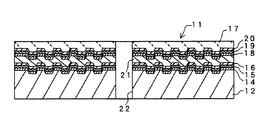
図2において、光ディスク(11)は、支持基体(12)の情報ピットやプリグルーブ等の微細凹凸が形成されている側の面上に、第2記録層用誘電体層(14)、第2記録層(レイヤー1)(15)、第2記録層用誘電体層(16)、スペーサー層(21)、第1記録層用誘電体層(18)、第1記録層(レイヤー0)(19)、第1記録層用誘電体層(20)をこの順で有し、前記誘電体層(20)上に光透過層(17)を有し、また中心孔(22)を有する。図示は省略されているが、支持基体(12)と誘電体層(14)との間、スペーサー層(21)と誘電体層(18)との間にそれぞれ反射層が設けられても良い。光ディスク(11)は、光透過層(17)を通して記録又は再生のためのレーザー光が入射するように使用される。
【0045】
次に、前述の本発明の光記録媒体の製造方法に用いることのできる好適な製造装置について、図3を参照して説明する。図3は、本発明の製造方法に用いることのできる好適な製造装置の概略を示す一部切り欠き平面図である。
【0046】
図3において、光記録媒体の製造装置は、支持基体上にエネルギー線硬化性樹脂を塗布しエネルギー線硬化性樹脂層を設けるスピンコーティング装置(31)と、前記エネルギー線硬化性樹脂層にエネルギー線照射を行い半硬化状態の樹脂層とする第1の紫外線照射装置(32)と、前記半硬化状態の樹脂層を加熱するアニール処理装置(33)と、アニール処理された前記半硬化状態の樹脂層にエネルギー線照射を行い完全硬化状態の樹脂層とする第2の紫外線照射装置(34)とを備えている。
【0047】
スピンコーティング装置(31)は、光透過層を形成すべきディスクを供給するディスク供給機(41)と、ディスクを載置し回転させる水平回転テーブル(42)と、ディスク表面にエネルギー線硬化性樹脂液を滴下する吐出ノズル(43)とを含む。ディスク供給機(41)は先端にディスクを吸着保持するためのバキュームパッドを有し、垂直上下運動及び90度の水平回転運動により、ディスクを搬送・供給できるようにされている。吐出ノズル(43)は、可逆回転する垂直回転軸(44)に固定された水平アーム(45)に取り付けられており、垂直回転軸(44)の回転と共に水平方向に回転するようになされている。また、吐出ノズル(43)には、塗布液供給管(46)を通じて塗布液が供給され、ノズル先端部から塗布液が滴下される。
【0048】
第1の紫外線照射装置(32)は、本体部(51)と、回転テーブル(42)上に載置されたディスク上方に設置された照射ヘッド(52)と、本体部(51)と照射ヘッド(52)とを連結する連結筒部(53)とを含む。本体部(51)内には紫外線光源としての超高圧水銀ランプが設置されている。本体部(51)内には更に、集光・送出光学系が設置されており、これにより、超高圧水銀ランプからの紫外線は集光され、連結筒部(53)に向かう紫外線ビームとして送出される。連結筒部(53)は筒体でありその内部にインテグレーターレンズが組み込まれており、紫外線ビームは筒部(53)を通過して照射ヘッド(52)に入射する。照射ヘッド(52)には反射板が内蔵されており、筒部(53)から入射した紫外線ビームを90度折り曲げて下方のディスクに向けて照射できるようにされている。
【0049】
アニール処理装置(33)は、アニールチャンバ(61)と、スピンコーティング装置(31)の回転テーブル(42)上のディスクをアニールチャンバ(61)の所定位置に搬送すると共に、アニール処理後のディスクを次工程の第2の紫外線照射装置(34)に搬送するコートハンド(65)とを含む。
【0050】
アニールチャンバ(61)には、回転テーブル(62)と、その上方に設置された適宜枚数の赤外線フラットパネルヒータ(64)とが備えられている。回転テーブル(62)はその外周付近に30度間隔で12枚のディスクを載置できるように12個のディスク支持部(63)が設けられ、テーブル(62)の中心周りに30度ずつ図示の例では反時計方向に間欠的に回転する。回転テーブル(62)下方には、回転のための適宜装置が設けられている。
【0051】
コートハンド(65)は、その垂直軸(65c) 周りに120度の範囲で回転可能とされている。コートハンド(65)は、図3に示された状態から時計方向に60度回転し、コートハンド(65)の一方のアーム(65a) が、回転テーブル(42)上のディスク上に位置する。この位置において、アーム(65a) の先端部に設けられた真空吸着機構により回転テーブル(42)上のディスクをピックアップする。その後、コートハンド(65)は、反時計方向に120度回転し、アーム(65a) が回転テーブル(62)の所定位置、すなわち63A と示されたディスク支持部の上に位置する。この位置において、ディスクの真空吸着を開放してディスクをディスク支持部(63)にセットする。
【0052】
また、コートハンド(65)の他方のアーム(65b) は、コートハンド(65)が図3に示された状態から時計方向に60度回転した際に、63A と示されたディスク支持部の上に位置する。この位置において、アーム(65b) の先端部に設けられた真空吸着機構により63A と示されたディスク支持部上のアニール処理済のディスクをピックアップする。その後、コートハンド(65)が反時計方向に120度回転した際に、アーム(65b) は、次に説明する第2の紫外線照射装置(34)のディスク移動機構(73)の73A と示された位置に来る。この位置において、ディスクの真空吸着を開放してディスクをディスク移動機構(73)の73A と示された位置にセットする。
【0053】
第2の紫外線照射装置(34)は、適宜支持部材(72)で支持された紫外線ランプ(71)と、ディスクを左方に直線移動させるディスク移動機構(73)と、光透過層が形成されたディスクを排出するディスク排出機(74)とを含む。ディスク移動機構(73)の詳細は示されないが、いわゆるコンベア式紫外線照射装置に備えられている公知の機構である。ディスクは73A の位置から73B の位置まで移動させられ、この間に、紫外線ランプ(71)からディスクに紫外線が照射されるようになされている。ディスク排出機(74)は、ディスク供給機(41)と同様の機構のものである。
【0054】
本発明において、まず、光透過層を形成すべき少なくとも1層の記録層が形成されたディスクを、ディスク供給機(41)により回転テーブル(42)上に載置し、真空吸着する。回転テーブル(42)上に載置されたディスク表面に、所定量のエネルギー線硬化性樹脂液を吐出ノズル(43)先端部から滴下する。滴下の際、ディスクは静止状態あるいは回転状態のいずれでもよい。次に、ディスクを高速で回転させてディスク表面に均一な膜厚の樹脂層を形成する。
【0055】
未硬化の樹脂層に照射ヘッド(52)から初回の紫外線照射を行い、所望の半硬化状態とする。この際、ディスクは回転されたままである。
【0056】
ディスクの回転を止め、コートハンド(65)の一方のアーム(65a) によって、ディスクをピックアップし、アニール処理装置(33)の回転テーブル(62)の所定位置、すなわち63A と示されたディスク支持部(63)にセットする。回転テーブル(62)を30度ずつ図示の例では反時計方向に間欠的に360度回転させ、その間に、アニールチャンバ(61)内においてディスクは所定の時間及び温度でアニール処理される。この時間及び温度は、適宜調整できる。
【0057】
アニール処理されて63A の位置に戻ってきたディスクを、コートハンド(65)の他方のアーム(65b) によってピックアップし、第2の紫外線照射装置(34)のディスク移動機構(73)の73A と示された位置にセットする。ディスクを73A の位置から73B の位置まで直線移動させ、この間に、紫外線ランプ(71)からディスクに紫外線を照射し、完全硬化の状態とする。このようにして、光透過層が形成される。
【0058】
この装置では、2回の紫外線照射とそれら照射の間のアニール処理を行うことができるが、3回以上の紫外線照射とそれら各回の照射の間のアニール処理を行うためには、さらにアニール処理装置と紫外線照射装置とを配置するか、あるいは、この装置を用いてアニール処理と紫外線照射の一連の処理を繰り返せばよい。
【0059】
【実施例】
以下に実施例を挙げて本発明をさらに具体的に説明するが、本発明は実施例に限定されるものではない。
【0060】
[実施例1](参考例)
以下の手順で光ディスクサンプルを作成した。
プリグルーブを形成したディスク状支持基体(ポリカーボネート製、直径120mm、厚さ1.1mm)の表面に、Agを主成分とする合金からなる厚さ100nmの反射層をスパッタリング法により形成した。グルーブの深さは、波長λ=405nmにおける光路長で表してλ/10とし、記録トラックピッチが0.3μmのランド/グルーブ基板とした。
【0061】
次いで、反射層表面に、ZnS(80モル%)−SiO2 (20モル%)ターゲットを用いて、スパッタリング法により厚さ30nmの誘電体層を形成した。次いで、この誘電体層表面に、相変化材料からなる合金ターゲットを用いて、スパッタリング法により厚さ12nmの記録層を形成した。記録層の組成は、GeSbTe系とした。
次いで、記録層表面に、ZnS(80モル%)−SiO2 (20モル%)ターゲットを用いて、スパッタリング法により厚さ100nmの誘電体層を形成した。この状態のディスクについて、株式会社コアーズ製機械精度測定機DC−1010Cにて機械特性(ディスク半径方向の反り角、ディスク円周方向の反り角)を測定した。
【0062】
測定後、上の誘電体層表面に、ウレタンアクリレートを主成分とする紫外線硬化性樹脂(硬化収縮率5.5%、25℃における粘度5000cP)をスピンコートにより塗布し、2000rpmで8秒間振り切り、厚さ100μmの未硬化の樹脂層を得た。
【0063】
この様にして形成した紫外線硬化性樹脂層に紫外線をUV積算光量140mJ/cm2 で照射し、半硬化状態の樹脂層を得た。その後、樹脂層に紫外線をUV積算光量3000mJ/cm2 で照射し、樹脂層を完全に硬化させ、光透過層を形成した。このように作成したディスクサンプルについて、前記のDC−1010Cにて機械特性(ディスク半径方向の反り角、ディスク円周方向の反り角)を測定した。
【0064】
[実施例2]
未硬化の樹脂層の形成までは、実施例1と同様に行った。紫外線硬化性樹脂層に紫外線をUV積算光量140mJ/cm2 で照射し、半硬化状態の樹脂層を得た。次に、60℃で3分間アニール処理を行い、その後、樹脂層に紫外線をUV積算光量3000mJ/cm2 で照射し、樹脂層を完全に硬化させ、光透過層を形成した。このように作成したディスクサンプルについて、前記のDC−1010Cにて機械特性を測定した。
【0065】
[比較例1]
未硬化の樹脂層の形成までは、実施例1と同様に行った。樹脂層を半硬化させることなく、樹脂層に紫外線をUV積算光量3000mJ/cm2 で照射し、樹脂層を完全に硬化させ、光透過層を形成した。このように作成したディスクサンプルについて、前記のDC−1010Cにて機械特性を測定した。
【0066】
[実施例3](参考例)
ウレタンアクリレートを主成分とする紫外線硬化性樹脂として、実施例1で用いた樹脂よりも硬化収縮がやや大きい樹脂(硬化収縮率5.9%、25℃における粘度5800cP)を用いた以外は、実施例1と同様にしてディスクサンプルを作成した。ディスクサンプルについて、前記のDC−1010Cにて機械特性を測定した。
【0067】
[実施例4]
紫外線硬化性樹脂として実施例3で用いた樹脂を用い、アニール処理温度を80℃とした以外は、実施例2と同様にしてディスクサンプルを作成した。ディスクサンプルについて、前記のDC−1010Cにて機械特性を測定した。
【0068】
[比較例2]
紫外線硬化性樹脂として実施例3で用いた樹脂を用いた以外は、比較例1と同様にしてディスクサンプルを作成した。ディスクサンプルについて、前記のDC−1010Cにて機械特性を測定した。
【0069】
【表1】

以上の測定結果を表1にまとめて示す。表1において、R−Skew (deg.) はディスク半径方向の反り角(°)を表し、T−Skew (deg.) はディスク円周方向の反り角(°)を表す。なお、測定機のレーザーヘッドにディスクの光透過層側が向くようにして、反り角を測定した。反りが光透過層側に凹の場合はプラス、逆の場合はマイナスの数値で表す。
ΔR−Skewは、光透過層の形成前から光透過層の形成後における変化量であり、ΔR−Skew=(光透過層形成後のR−Skew)−(光透過層形成前のR−Skew)である。同様に、ΔT−Skew=(光透過層形成後のT−Skew)−(光透過層形成前のT−Skew)である。
【0071】
なお、実施例1、2、及び比較例1における光透過層形成前のR−Skew値、T−Skew値は、同一の値となるべきであるが、現実に測定された値には僅かなバラツキが見られた。実施例3、4、及び比較例2においても同様に、僅かなバラツキが見られた。
【0072】
表1より、実施例1〜4のいずれのディスクサンプルも、紫外線照射による樹脂の硬化収縮が非常に抑制され、光透過層の形成前後における反り角の変化量が小さく、機械特性に優れていた。特に、実施例4では、硬化収縮度合いがやや大きい樹脂を用いたにも係わらず、的確なアニール処理を行ったので、ディスクサンプルは機械特性に優れていた。
【0073】
【発明の効果】
本発明によれば、0.1mm(100μm)程度の厚さの光透過層を光硬化性樹脂を用いて形成し、機械特性に優れた光記録媒体を製造することができる。また、本発明によれば、前記方法に用いることのできる好適な光記録媒体の製造装置が提供される。
【図面の簡単な説明】
【図1】 本発明の方法により製造される光ディスクの一例の概略断面図である。
【図2】 本発明の方法により製造される光ディスクの他の一例の概略断面図である。
【図3】 本発明の製造方法に用いることのできる好適な製造装置の概略を示す一部切り欠き平面図である。
【符号の説明】
(1) :光ディスク
(2) :支持基体
(3) :反射層
(4) :誘電体層
(5) :記録層
(6) :誘電体層
(7) :光透過層
(8) :中心孔
(31):スピンコーティング装置
(32):第1の紫外線照射装置
(33):アニール処理装置
(34):第2の紫外線照射装置[0001]
BACKGROUND OF THE INVENTION
The present invention relates to a method for manufacturing an optical recording medium, and more particularly to a method for manufacturing an optical recording medium having a light transmission layer formed of an energy ray curable resin on a recording layer. The present invention also relates to a suitable manufacturing apparatus that can be used in the method for manufacturing the optical recording medium.
[0002]
[Prior art]
In recent years, in optical recording media, it has been necessary to further increase the recording density for enormous information processing such as moving image information, and research and development has been actively conducted to further increase the recording capacity. .
[0003]
One of them is to shorten the wavelength of the recording / reproducing laser light, to increase the numerical aperture (NA) of the objective lens, and to reduce the spot diameter during recording / reproducing, as seen on DVDs, for example. Has been done. Actually, in a DVD, the recording / reproducing wavelength λ is changed from 780 nm to 650 nm of the CD, and the numerical aperture (NA) is changed from 0.45 to 0.6 of the CD, so that the recording capacity (6. 7GB / surface).
[0004]
However, various problems arise due to such high NA. For example, an allowable amount of aberration caused by an angle at which the disk surface deviates from the optical axis of the optical pickup, that is, a so-called tilt angle, becomes small. Here, assuming that the wavelength of the recording / reproducing laser beam is λ and the thickness of the substrate is t, the tolerance of the tilt of the optical recording medium with respect to the optical system, the so-called tilt margin M, is determined by the numerical aperture NA. That is, the tilt margin M is λ / {t × (NA)Three}. In order to ensure the tilt margin M, it is necessary to reduce the thickness t of the substrate.
[0005]
Therefore, in the DVD, the thickness of the substrate is about half (about 0.6 mm) of the thickness of the conventional CD substrate (about 1.2 mm), thereby ensuring a tilt margin.
[0006]
Recently, in order to record a high-quality moving image for a long time, the wavelength λ of the recording / reproducing laser beam is further shortened to about 400 nm and the numerical aperture (NA) is increased to 0.85, which is four times that of DVD. Development of a system that attempts to achieve a high recording capacity (> 20 GB / surface), which is the above recording capacity, has been underway.
[0007]
In this system, recording / reproducing light is irradiated not through the substrate side but through a light transmission layer set to a thickness of about 0.1 mm. An optical recording medium having such a light transmission layer is described in, for example, Japanese Patent Laid-Open No. 10-289489, and the medium described in the same publication has a light transmission layer made of a photocurable resin.
[0008]
[Patent Document 1]
Japanese Patent Laid-Open No. 10-289489
[0009]
[Problems to be solved by the invention]
On the other hand, in conventional optical recording media such as CDs and DVDs, an energy ray curable resin is used for the protective layer, and there is a problem of an increase in warpage due to the curing shrinkage of the resin. Various studies have been conducted. However, the coating thickness of the energy ray curable resin of the protective layer is about 2 μm to 20 μm, and the study of a thick film thickness exceeding this is not sufficient.
[0010]
That is, when a light transmission layer having a thickness of about 0.1 mm (100 μm) is formed from an energy ray curable resin, it is considered difficult to solve the problem of curing shrinkage only by improving the resin material. .
[0011]
Accordingly, an object of the present invention is to provide a method for producing an optical recording medium having excellent mechanical properties by forming a light transmission layer using an energy ray curable resin.
Another object of the present invention is to provide a suitable optical recording medium manufacturing apparatus that can be used in the above method.
[0012]
[Means for Solving the Problems]
As a result of intensive studies, the inventors of the present invention use an energy ray curable resin having a relatively small degree of curing shrinkage to cure the resin stepwise to disperse the stress generated by the curing shrinkage and to accumulate the stress on the disk. As a result, the present inventors have found that an optical recording medium excellent in mechanical properties can be obtained in which the deformation of the disk is extremely suppressed, and the present invention has been achieved.
The present inventors have further found that an optical information medium having further excellent mechanical characteristics can be obtained by once releasing the stress accumulated in the disk by annealing and then curing it again.
[0013]
The present invention is a method for producing an optical recording medium having at least one recording layer and a light transmission layer on a recording layer on a support substrate, and an energy ray curable resin layer is provided on the recording layer, This resin layer is irradiated with energy rays at least twice.In addition, an annealing process (thermal relaxation process) is performed between any one of the energy beam irradiations and the next energy beam irradiation.Thus, a method for producing an optical recording medium, characterized in that a light transmission layer is formed.
[0014]
The present invention is the above-described method for manufacturing an optical recording medium, wherein the integrated light quantity of each time of energy beam irradiation is increased stepwise between each time.
The present invention is the above-described method for producing an optical recording medium, wherein the energy rays are ultraviolet rays.
[0015]
BookThe present invention is the above-described method for manufacturing an optical recording medium, wherein the annealing process is performed at a temperature of 60 ° C. or higher.
[0016]
The present invention is the method for manufacturing an optical recording medium, wherein the light transmission layer has a thickness of 20 to 200 μm.
[0017]
The present invention also provides an application means for applying an energy beam curable resin on a support substrate to provide an energy beam curable resin layer, and a semi-cured resin layer by irradiating the energy beam curable resin layer with an energy beam. A first energy ray irradiating means, an annealing treatment means for heating the semi-cured resin layer, and the annealed semi-cured resin layer is irradiated with energy rays to form a fully cured resin layer. An apparatus for manufacturing an optical recording medium, comprising: a second energy beam irradiation unit.
[0018]
DETAILED DESCRIPTION OF THE INVENTION
A method for manufacturing an optical recording medium (hereinafter abbreviated as an optical disk) will be described with reference to the drawings. Hereinafter, a phase change type optical disc will be described as an example. However, the present invention is not limited to this, and can be widely applied regardless of the type of recording layer, such as a read-only optical disc and an optical disc that can be recorded only once.
[0019]
FIG. 1 is a schematic cross-sectional view of an example of an optical disk manufactured by the method of the present invention. In FIG. 1, an optical disk (1) has a reflective layer (3), a dielectric layer (4), a recording layer on the surface of a support base (2) on which fine irregularities such as information pits and pregrooves are formed. The layer (5) and the dielectric layer (6) are provided in this order, the light transmission layer (7) is provided on the dielectric layer (6), and the center hole (8) is provided. The optical disk (1) is used so that laser light for recording or reproduction enters through the light transmission layer (7).
[0020]
The support substrate (2) has a thickness of 0.3 to 1.6 mm, preferably 0.5 to 1.3 mm, and has information pits and pregrooves on the surface on which the recording layer (5) is formed. Etc. are formed.
The support substrate (2) does not need to be optically transparent, and various plastic materials such as polycarbonate resins, acrylic resins such as polymethyl methacrylate (PMMA), polyolefin resins, and the like can be used. When such a material that is easily bent is used, the present invention is particularly effective because the occurrence of warpage can be suppressed. However, glass, ceramics, metal or the like may be used. In the case of using a plastic material, the concavo-convex pattern is often created by injection molding, and in the case of other than the plastic material, it is formed by a photopolymer method (2P method).
[0021]
On the support substrate (2), the reflective layer (3) is usually formed by sputtering. As a material for the reflective layer, a metal element, a metalloid element, a semiconductor element, or a compound thereof is used alone or in combination. Specifically, for example, a known reflective layer material such as Au, Ag, Cu, Al, or Pd may be selected. The reflective layer is preferably formed as a thin film having a thickness of 20 to 200 nm.
[0022]
The dielectric layer (4), the recording layer (5), and the dielectric layer (6) are sputtered in this order on the reflective layer (3) or directly on the support substrate (2) when there is no reflective layer. It is formed by.
[0023]
The recording layer (5) is reversibly changed between a crystalline state and an amorphous state by laser light irradiation, and is formed of a material having different optical characteristics between the two states. For example, Ge—Sb—Te, In—Sb—Te, Sn—Se—Te, Ge—Te—Sn, In—Se—Tl, In—Sb—Te, and the like can be given. Further, these materials contain a trace amount of at least one of metals selected from Co, Pt, Pd, Au, Ag, Ir, Nb, Ta, V, W, Ti, Cr, Zr, Bi, In, and the like. It may be added, or a reducing gas such as nitrogen may be added in a trace amount.
The thickness of the recording layer (5) is not particularly limited and is, for example, about 3 to 50 nm.
[0024]
The dielectric layer (4) and the dielectric layer (6) are formed on both sides of the upper and lower sides of the recording layer (5). The dielectric layer (4) and the dielectric layer (6) have a function as an interference layer for adjusting optical characteristics as well as mechanical and chemical protection functions of the recording layer (5). Each of the dielectric layer (4) and the dielectric layer (6) may be composed of a single layer or a plurality of layers.
[0025]
The dielectric layer (4) and the dielectric layer (6) are selected from Si, Zn, Al, Ta, Ti, Co, Zr, Pb, Ag, Zn, Sn, Ca, Ce, V, Cu, Fe, and Mg. It is preferably formed from an oxide, a nitride, a sulfide, a fluoride, or a composite thereof containing at least one of the metals. The extinction coefficient k of the dielectric layer (4) and the dielectric layer (6) is preferably 0.1 or less.
[0026]
The thickness of the dielectric layer (4) is not particularly limited, and is preferably about 20 to 150 nm, for example. The thickness of the dielectric layer (6) is not particularly limited, and is preferably about 20 to 200 nm, for example. By selecting the thickness of the dielectric layers (4) and (6) within such a range, the reflection can be adjusted.
[0027]
A light transmission layer (7) is formed on the dielectric layer (6) using an energy ray curable resin.
[0028]
Energy ray curable resin is selected from UV curable resin and electron beam curable resin, provided that it is optically transparent, has little optical absorption and reflection in the laser wavelength range used, and has low birefringence. To do.
[0029]
Specifically, it is preferably composed of an ultraviolet (electron beam) curable compound or a composition for polymerization thereof. Examples of such compounds include ester compounds of acrylic acid and methacrylic acid, acrylic double bonds such as epoxy acrylate and urethane acrylate, allyl double bonds such as diallyl phthalate, and unsaturated double bonds such as maleic acid derivatives. Mention may be made of monomers, oligomers, polymers and the like containing or introduced in the molecule a group which crosslinks or polymerizes upon irradiation with ultraviolet rays such as bonds. These are preferably polyfunctional, particularly trifunctional or more, and may be used alone or in combination of two or more.
[0030]
As the UV curable monomer, a compound having a molecular weight of less than 2000 is preferable, and as the oligomer, a molecular weight of 2000 to 10,000 is preferable. Examples of these include styrene, ethyl acrylate, ethylene glycol diacrylate, ethylene glycol dimethacrylate, diethylene glycol diacrylate, diethylene glycol methacrylate, 1,6-hexane glycol diacrylate, 1,6-hexane glycol dimethacrylate, and the like. Examples thereof include pentaerythritol tetra (meth) acrylate, pentaerythritol (meth) acrylate, trimethylolpropane tri (meth) acrylate, trimethylolpropane di (meth) acrylate, and (meth) acrylate of a phenol ethylene oxide adduct. In addition, examples of the ultraviolet curable oligomer include oligoester acrylate and an acrylic modified product of urethane elastomer.
[0031]
Moreover, as an ultraviolet curable material, the composition containing an epoxy resin and a photocationic polymerization catalyst is also used suitably. As the epoxy resin, alicyclic epoxy resins are preferable, and those having two or more epoxy groups in the molecule are particularly preferable. Examples of alicyclic epoxy resins include 3,4-epoxycyclohexylmethyl-3,4-epoxycyclohexanecarboxylate, bis- (3,4-epoxycyclohexylmethyl) adipate, bis- (3,4-epoxycyclohexyl) adipate, One or more of 2- (3,4-epoxycyclohexyl-5,5-spiro-3,4-epoxy) cyclohexane-meta-dioxane, bis (2,3-epoxycyclopentyl) ether, vinylcyclohexene dioxide and the like are preferable. . Although there is no restriction | limiting in particular in the epoxy equivalent of an alicyclic epoxy resin, Since favorable sclerosis | hardenability is acquired, it is preferable that it is 60-300, especially 100-200.
[0032]
Any known photocationic polymerization catalyst may be used without any particular limitation. For example, one or more metal fluoroborate and boron trifluoride complexes, bis (perfluoroalkylsulfonyl) methane metal salts, aryldiazonium compounds, 6A group aromatic onium salts, 5A group aromatic onium salts, Dicarbonyl chelate, thiopyrylium salt of group 3A-5A element, group 6A element having MF6 anion (where M is P, As or Sb), triarylsulfonium complex salt, aromatic iodonium complex salt, aromatic sulfonium complex salt, etc. are used. In particular, it is preferable to use one or more of polyarylsulfonium complex salts, aromatic sulfonium salts or iodonium salts of halogen-containing complex ions, aromatic onium salts of group 3A elements, group 5A elements and group 6A elements.
[0033]
As a radiation curable resin used for a light transmissive layer, what has a viscosity (25 degreeC) of 1,000-10,000cp is preferable.
[0034]
In the present invention, an energy ray curable resin is applied on the dielectric layer (6) to provide an uncured energy ray curable resin layer. Application at this time may be performed by a spin coating method.
[0035]
Next, energy ray irradiation is performed in a plurality of times on the uncured energy ray-curable resin layer, and the resin is cured stepwise. That is, at least two irradiations of energy rays are performed: irradiation until the semi-cured state before complete curing and irradiation from the semi-cured state to the fully cured state. As energy rays, ultraviolet rays or electron beams are used depending on the resin used.
[0036]
The first energy beam irradiation is performed with an integrated light amount that leaves a tack on the surface of the resin layer, and the resin is in a semi-cured state. Although it differs depending on the resin material, it can be achieved by shortening the irradiation time or reducing the irradiation intensity as compared with the case of complete curing by one irradiation. Such energy beam irradiation before complete curing is performed once or twice or more. When performing irradiation twice or more before complete curing, the integrated light quantity of each energy ray irradiation is increased step by step between each time.
[0037]
Next, in order to finally completely cure the resin, the final energy beam irradiation is performed with an integrated light amount that is greater than any integrated light amount of each energy beam irradiation before complete curing, and the resin is completely cured. Put it in a state. This can be achieved by lengthening the irradiation time or increasing the irradiation intensity compared to each irradiation before complete curing.
[0038]
The integrated light amount of each energy ray irradiation varies depending on the resin material, the thickness of the resin layer, and the like. For example, when performing the irradiation twice, the integrated light amount of the first energy ray irradiation is 5 to 300 mJ / cm.2Integrated light quantity of the second energy beam irradiation 500 to 5000 mJ / cm2To the extent.
[0039]
In this way, by curing the resin stepwise, it is possible to reduce the stress due to curing shrinkage that accumulates on the disk at a time, and finally the stress that accumulates on the disk is reduced. As a result, even if the thickness of the light transmission layer (7) is 20 μm or more and 200 μm or less, particularly 70 μm or more and 150 μm or less, and more particularly 75 μm or more and 150 μm or less, a disk having excellent mechanical properties is produced. Can do.
[0040]
Further, the stress due to curing shrinkage is maximized at the moment when the resin is cured, and is relieved with the passage of time. For this reason, it is possible to further reduce the stress accumulated by curing shrinkage by releasing the stress accumulated in the disk and then performing the next curing. However, since it is not productive to spend time until the stress is released in a semi-cured state, it is possible to release the stress in a short time by performing an annealing process, and then irradiate the energy ray again to be cured. That is, in the present invention,Any timeEnergy beam irradiation and the next of this irradiationTimesAn annealing process is performed between energy beam irradiationYeah. DWhen performing energy beam irradiation three or more times, annealing treatment is performed at the end of each irradiation, such as between the first irradiation and the second irradiation, and between the second irradiation and the third irradiation. It is preferable to perform the step from the viewpoint of releasing the curing shrinkage stress.
[0041]
The annealing temperature is preferably 60 ° C. or higher, and more preferably 80 ° C. or higher. By setting the annealing temperature to 80 ° C. or higher, the stress can be released more quickly and completely. Although the upper limit of the annealing temperature depends on the material of the supporting substrate to be used, it is preferably performed at a temperature that is at least 10 ° C. lower than the glass transition temperature Tg of a generally used material. Also, the annealing treatment time is preferably 1 to 5 minutes from the viewpoint of production efficiency, though it depends on the annealing treatment temperature.
By performing the annealing process in this way, a disk having further excellent mechanical characteristics can be produced.
[0042]
Further, in the present invention, an uncured energy beam curable resin layer having a thickness corresponding to a part of the target thickness of the light transmission layer (7) is formed, and the resin is semi-cured by performing energy beam irradiation. As a state, on the semi-cured resin layer, a layer of the same resin having a thickness corresponding to the remainder of the target thickness is formed by overcoating, and then energy beam irradiation is performed to form a semi-cured resin layer. It is possible to completely cure the uncured resin layer. If it does in this way, mixing will occur in the interface of two resin layers, and it can raise the adhesiveness between both resin layers.
[0043]
As described above, the manufacturing method of the present invention has been described using the optical disk shown in FIG. 1 as an example. However, the manufacturing method of the present invention is also applied to the so-called single-sided, double-layered optical disk shown in FIG.
[0044]
In FIG. 2, the optical disk (11) has a second recording layer dielectric layer (14) and a second recording layer on the surface of the support substrate (12) on which fine irregularities such as information pits and pregrooves are formed. Recording layer (layer 1) (15), dielectric layer for second recording layer (16), spacer layer (21), dielectric layer for first recording layer (18), first recording layer (layer 0) (19 ), A first recording layer dielectric layer (20) in this order, a light transmission layer (17) on the dielectric layer (20), and a central hole (22). Although not shown, a reflective layer may be provided between the support base (12) and the dielectric layer (14) and between the spacer layer (21) and the dielectric layer (18). The optical disk (11) is used so that laser light for recording or reproduction enters through the light transmission layer (17).
[0045]
Next, a suitable manufacturing apparatus that can be used in the above-described optical recording medium manufacturing method of the present invention will be described with reference to FIG. FIG. 3 is a partially cutaway plan view showing an outline of a suitable manufacturing apparatus that can be used in the manufacturing method of the present invention.
[0046]
In FIG. 3, an optical recording medium manufacturing apparatus includes a spin coating apparatus (31) that applies an energy ray curable resin on a support substrate and provides an energy ray curable resin layer, and an energy ray curable resin layer on the energy ray curable resin layer. A first ultraviolet irradiation device (32) that irradiates and forms a semi-cured resin layer; an annealing treatment device (33) that heats the semi-cured resin layer; and the semi-cured resin that has been annealed. And a second ultraviolet irradiation device (34) for irradiating the layer with energy rays to form a completely cured resin layer.
[0047]
The spin coating apparatus (31) includes a disk feeder (41) for supplying a disk on which a light transmission layer is to be formed, a horizontal rotary table (42) for mounting and rotating the disk, and an energy beam curable resin on the disk surface. And a discharge nozzle (43) for dropping the liquid. The disk feeder (41) has a vacuum pad for adsorbing and holding the disk at the tip, and is capable of conveying and supplying the disk by vertical vertical movement and horizontal rotation movement of 90 degrees. The discharge nozzle (43) is attached to a horizontal arm (45) fixed to a vertically rotating shaft (44) that rotates reversibly, and rotates in the horizontal direction along with the rotation of the vertically rotating shaft (44). . In addition, the application liquid is supplied to the discharge nozzle (43) through the application liquid supply pipe (46), and the application liquid is dropped from the nozzle tip.
[0048]
The first ultraviolet irradiation device (32) includes a main body (51), an irradiation head (52) installed above a disk placed on the rotary table (42), a main body (51), and an irradiation head. And a connecting tube portion (53) for connecting (52). An ultra high pressure mercury lamp as an ultraviolet light source is installed in the main body (51). Further, a condensing / sending optical system is installed in the main body (51), so that the ultraviolet rays from the ultra-high pressure mercury lamp are condensed and sent out as an ultraviolet beam directed to the connecting tube portion (53). The The connecting cylinder part (53) is a cylinder and an integrator lens is incorporated therein, and the ultraviolet beam passes through the cylinder part (53) and enters the irradiation head (52). The irradiation head (52) has a built-in reflecting plate so that the ultraviolet beam incident from the cylindrical portion (53) can be bent 90 degrees and irradiated toward the lower disk.
[0049]
The annealing apparatus (33) transports the disk on the rotating table (42) of the annealing chamber (61) and the spin coating apparatus (31) to a predetermined position of the annealing chamber (61), and the disk after the annealing process. And a coat hand (65) transported to the second ultraviolet irradiation device (34) in the next step.
[0050]
The annealing chamber (61) includes a rotary table (62) and an appropriate number of infrared flat panel heaters (64) installed above the rotary table (62). The rotary table (62) is provided with twelve disc support portions (63) so that twelve discs can be placed in the vicinity of the outer periphery of the rotary table (62). In the example, it rotates intermittently counterclockwise. An appropriate device for rotation is provided below the rotary table (62).
[0051]
The coat hand (65) is rotatable about a vertical axis (65c) within a range of 120 degrees. The coat hand (65) is rotated 60 degrees clockwise from the state shown in FIG. 3, and one arm (65a) of the coat hand (65) is positioned on the disk on the rotary table (42). At this position, the disk on the rotary table (42) is picked up by a vacuum suction mechanism provided at the tip of the arm (65a). Thereafter, the coat hand (65) rotates 120 degrees counterclockwise, and the arm (65a) is positioned on a predetermined position of the rotary table (62), that is, on the disk support portion indicated by 63A. At this position, the vacuum suction of the disc is released and the disc is set on the disc support (63).
[0052]
Further, the other arm (65b) of the coat hand (65) is placed on the disk support portion indicated by 63A when the coat hand (65) is rotated 60 degrees clockwise from the state shown in FIG. Located in. At this position, the annealed disc on the disc support portion indicated as 63A is picked up by a vacuum suction mechanism provided at the tip of the arm (65b). Thereafter, when the coated hand (65) is rotated 120 degrees counterclockwise, the arm (65b) is indicated as 73A of the disk moving mechanism (73) of the second ultraviolet irradiation device (34) described below. Come to the position. At this position, the vacuum suction of the disk is released and the disk is set at a position indicated by 73A of the disk moving mechanism (73).
[0053]
The second ultraviolet irradiation device (34) includes an ultraviolet lamp (71) supported by a support member (72) as appropriate, a disk moving mechanism (73) that linearly moves the disk to the left, and a light transmission layer. A disc ejector (74) for ejecting the disc. Although details of the disk moving mechanism (73) are not shown, it is a known mechanism provided in a so-called conveyor type ultraviolet irradiation device. The disk is moved from the position of 73A to the position of 73B, and during this time, the ultraviolet light is irradiated to the disk from the ultraviolet lamp (71). The disc ejector (74) has the same mechanism as the disc feeder (41).
[0054]
In the present invention, first, a disc having at least one recording layer on which a light transmission layer is to be formed is placed on a rotary table (42) by a disc feeder (41) and vacuum-sucked. A predetermined amount of energy beam curable resin liquid is dropped from the tip of the discharge nozzle (43) onto the surface of the disk placed on the rotary table (42). At the time of dropping, the disk may be either stationary or rotating. Next, the disk is rotated at a high speed to form a resin layer having a uniform film thickness on the disk surface.
[0055]
The uncured resin layer is irradiated with ultraviolet rays for the first time from the irradiation head (52) to obtain a desired semi-cured state. At this time, the disc remains rotated.
[0056]
Stop the rotation of the disk, pick up the disk by one arm (65a) of the coat hand (65), and place it at a predetermined position on the rotary table (62) of the annealing apparatus (33), that is, 63A. Set to (63). In the illustrated example, the rotary table (62) is intermittently rotated 360 degrees counterclockwise in the illustrated example, while the disk is annealed in the annealing chamber (61) at a predetermined time and temperature. This time and temperature can be appropriately adjusted.
[0057]
The disk which has been annealed and returned to the position of 63A is picked up by the other arm (65b) of the coat hand (65) and indicated as 73A of the disk moving mechanism (73) of the second ultraviolet irradiation device (34). Set to the specified position. The disk is linearly moved from the position of 73A to the position of 73B, and during this time, the disk is irradiated with ultraviolet rays from the ultraviolet lamp (71) to be in a completely cured state. In this way, a light transmission layer is formed.
[0058]
In this apparatus, it is possible to perform two ultraviolet irradiations and an annealing process between these irradiations. In order to perform an annealing process between three or more ultraviolet irradiations and each of these irradiations, an annealing apparatus is further provided. And an ultraviolet irradiation device, or a series of processes of annealing and ultraviolet irradiation may be repeated using this device.
[0059]
【Example】
EXAMPLES Hereinafter, the present invention will be described more specifically with reference to examples, but the present invention is not limited to the examples.
[0060]
[Example 1](Reference example)
An optical disc sample was prepared according to the following procedure.
A reflective layer having a thickness of 100 nm made of an alloy containing Ag as a main component was formed on the surface of a disk-shaped support substrate (made of polycarbonate, diameter 120 mm, thickness 1.1 mm) on which pregrooves were formed. The depth of the groove was expressed as an optical path length at a wavelength λ = 405 nm, λ / 10, and a land / groove substrate having a recording track pitch of 0.3 μm was used.
[0061]
Subsequently, ZnS (80 mol%)-SiO2 is formed on the reflective layer surface.2A dielectric layer having a thickness of 30 nm was formed by sputtering using a (20 mol%) target. Next, a recording layer having a thickness of 12 nm was formed on the surface of the dielectric layer by sputtering using an alloy target made of a phase change material. The composition of the recording layer was GeSbTe.
Next, ZnS (80 mol%)-SiO is formed on the surface of the recording layer.2A dielectric layer having a thickness of 100 nm was formed by sputtering using a (20 mol%) target. With respect to the disk in this state, mechanical characteristics (a warp angle in the disk radial direction and a warp angle in the disk circumferential direction) were measured with a machine precision measuring machine DC-1010C manufactured by Cores Co., Ltd.
[0062]
After the measurement, an ultraviolet curable resin (curing shrinkage: 5.5%, viscosity: 5000 cP at 25 ° C.) mainly composed of urethane acrylate was applied to the upper dielectric layer surface by spin coating, and shaken off at 2000 rpm for 8 seconds. An uncured resin layer having a thickness of 100 μm was obtained.
[0063]
Ultraviolet rays are applied to the ultraviolet curable resin layer formed in this way, and the UV integrated light quantity is 140 mJ / cm.2And a semi-cured resin layer was obtained. After that, ultraviolet rays are applied to the resin layer, and the UV integrated light quantity is 3000 mJ / cm2The resin layer was completely cured to form a light transmission layer. The disk samples thus prepared were measured for mechanical properties (the warp angle in the disk radial direction and the warp angle in the disk circumferential direction) using the DC-1010C.
[0064]
[Example 2]
The same procedure as in Example 1 was performed until the uncured resin layer was formed. UV integrated light quantity 140mJ / cm2And a semi-cured resin layer was obtained. Next, an annealing treatment is performed at 60 ° C. for 3 minutes, and then ultraviolet rays are applied to the resin layer with a UV integrated light amount of 3000 mJ / cm2The resin layer was completely cured to form a light transmission layer. The disk sample thus prepared was measured for mechanical properties using the DC-1010C.
[0065]
[Comparative Example 1]
The same procedure as in Example 1 was performed until the uncured resin layer was formed. Without semi-curing the resin layer, UV light is applied to the resin layer with a UV integrated light amount of 3000 mJ / cm.2The resin layer was completely cured to form a light transmission layer. The disk sample thus prepared was measured for mechanical properties using the DC-1010C.
[0066]
[Example 3](Reference example)
Except for using UV curable resin mainly composed of urethane acrylate, a resin having a slightly higher cure shrinkage than the resin used in Example 1 (curing shrinkage 5.9%, viscosity 5800 cP at 25 ° C.) was used. A disk sample was prepared in the same manner as in Example 1. The disk sample was measured for mechanical properties using the DC-1010C.
[0067]
[Example 4]
A disk sample was prepared in the same manner as in Example 2 except that the resin used in Example 3 was used as the ultraviolet curable resin and the annealing temperature was 80 ° C. The disk sample was measured for mechanical properties using the DC-1010C.
[0068]
[Comparative Example 2]
A disk sample was prepared in the same manner as in Comparative Example 1 except that the resin used in Example 3 was used as the ultraviolet curable resin. The disk sample was measured for mechanical properties using the DC-1010C.
[0069]
[Table 1]
The above measurement results are summarized in Table 1. In Table 1, R-Skew (deg.) Represents the warp angle (°) in the disk radial direction, and T-Skew (deg.) Represents the warp angle (°) in the disk circumferential direction. The warp angle was measured such that the light transmission layer side of the disk was facing the laser head of the measuring machine. When the warp is concave on the light transmitting layer side, the value is plus, and when the warp is opposite, the value is minus.
ΔR-Skew is the amount of change after formation of the light transmission layer from before formation of the light transmission layer, and ΔR-Skew = (R-Skew after formation of the light transmission layer) − (R-Skew before formation of the light transmission layer). ). Similarly, ΔT-Skew = (T-Skew after formation of the light transmission layer) − (T-Skew before formation of the light transmission layer).
[0071]
It should be noted that the R-Skew value and T-Skew value before formation of the light transmission layer in Examples 1 and 2 and Comparative Example 1 should be the same value, but the values actually measured are a little. Variations were seen. Similarly, in Examples 3 and 4 and Comparative Example 2, slight variations were observed.
[0072]
From Table 1, in any of the disk samples of Examples 1 to 4, the curing shrinkage of the resin due to ultraviolet irradiation was greatly suppressed, the change amount of the warp angle before and after the formation of the light transmission layer was small, and the mechanical properties were excellent. . In particular, in Example 4, despite the use of a resin having a slightly high degree of cure shrinkage, an accurate annealing treatment was performed, so that the disk sample was excellent in mechanical properties.
[0073]
【The invention's effect】
According to the present invention, an optical recording medium having excellent mechanical properties can be manufactured by forming a light transmission layer having a thickness of about 0.1 mm (100 μm) using a photocurable resin. The present invention also provides a suitable optical recording medium manufacturing apparatus that can be used in the above method.
[Brief description of the drawings]
FIG. 1 is a schematic cross-sectional view of an example of an optical disk manufactured by the method of the present invention.
FIG. 2 is a schematic cross-sectional view of another example of an optical disc manufactured by the method of the present invention.
FIG. 3 is a partially cutaway plan view showing an outline of a suitable manufacturing apparatus that can be used in the manufacturing method of the present invention.
[Explanation of symbols]
(1): Optical disc
(2): Support base
(3): Reflective layer
(4): Dielectric layer
(5): Recording layer
(6): Dielectric layer
(7): Light transmission layer
(8): Center hole
(31): Spin coating equipment
(32): First ultraviolet irradiation device
(33): Annealing equipment
(34): Second ultraviolet irradiation device
Claims (6)
前記エネルギー線硬化性樹脂層にエネルギー線照射を行い半硬化状態の樹脂層とする第1のエネルギー線照射手段と、
前記半硬化状態の樹脂層を加熱するアニール処理手段と、
アニール処理された前記半硬化状態の樹脂層にエネルギー線照射を行い完全硬化状態の樹脂層とする第2のエネルギー線照射手段とを備える、光記録媒体の製造装置。An application means for applying an energy ray curable resin on a support substrate and providing an energy ray curable resin layer;
A first energy ray irradiation means for irradiating the energy ray curable resin layer with an energy ray to form a semi-cured resin layer;
Annealing treatment means for heating the semi-cured resin layer;
An apparatus for manufacturing an optical recording medium, comprising: a second energy ray irradiating unit that irradiates the annealed semi-cured resin layer with energy rays to form a completely cured resin layer.
Priority Applications (1)
| Application Number | Priority Date | Filing Date | Title |
|---|---|---|---|
| JP2002268685A JP3977711B2 (en) | 2001-09-13 | 2002-09-13 | Optical recording medium manufacturing method and manufacturing apparatus |
Applications Claiming Priority (3)
| Application Number | Priority Date | Filing Date | Title |
|---|---|---|---|
| JP2001-278557 | 2001-09-13 | ||
| JP2001278557 | 2001-09-13 | ||
| JP2002268685A JP3977711B2 (en) | 2001-09-13 | 2002-09-13 | Optical recording medium manufacturing method and manufacturing apparatus |
Publications (3)
| Publication Number | Publication Date |
|---|---|
| JP2003162847A JP2003162847A (en) | 2003-06-06 |
| JP2003162847A5 JP2003162847A5 (en) | 2005-11-04 |
| JP3977711B2 true JP3977711B2 (en) | 2007-09-19 |
Family
ID=26622170
Family Applications (1)
| Application Number | Title | Priority Date | Filing Date |
|---|---|---|---|
| JP2002268685A Expired - Fee Related JP3977711B2 (en) | 2001-09-13 | 2002-09-13 | Optical recording medium manufacturing method and manufacturing apparatus |
Country Status (1)
| Country | Link |
|---|---|
| JP (1) | JP3977711B2 (en) |
Families Citing this family (5)
| Publication number | Priority date | Publication date | Assignee | Title |
|---|---|---|---|---|
| TWI363343B (en) | 2003-12-10 | 2012-05-01 | Panasonic Corp | Optical information recording medium |
| TWI437054B (en) * | 2006-12-08 | 2014-05-11 | Nippon Catalytic Chem Ind | Composition for coating material |
| JP5139721B2 (en) * | 2007-06-08 | 2013-02-06 | 株式会社日本触媒 | Hard coat materials and laminates |
| JP5448333B2 (en) * | 2006-12-08 | 2014-03-19 | 株式会社日本触媒 | Resin composition for hard coat material and laminate |
| US8399583B2 (en) | 2008-03-05 | 2013-03-19 | Nippon Shokubai Co., Ltd. | Polymer, curable resin composition, cured product, and article |
-
2002
- 2002-09-13 JP JP2002268685A patent/JP3977711B2/en not_active Expired - Fee Related
Also Published As
| Publication number | Publication date |
|---|---|
| JP2003162847A (en) | 2003-06-06 |
Similar Documents
| Publication | Publication Date | Title |
|---|---|---|
| EP0611473B1 (en) | Optical disc master | |
| JP3977711B2 (en) | Optical recording medium manufacturing method and manufacturing apparatus | |
| US20040246884A1 (en) | Optical recording medium manufacturing method | |
| TWI284898B (en) | Manufacturing method optical recording media and optical recording media | |
| EP2209119B1 (en) | Optical information recording medium | |
| EP1564734B1 (en) | Method for producing stamper used for producing optical disc and optical disc producing method | |
| TWI338892B (en) | Optical information medium and method for manufacturing the same | |
| JP2004160742A (en) | Optical recording disc, its manufacturing method and optical data recording/ reproducing method for optical recording disc | |
| US8767520B2 (en) | Method of producing recording medium, and recording medium | |
| US9196288B2 (en) | Process and apparatus for producing optical recording medium | |
| WO2007058309A2 (en) | Method and apparatus for producing optical recording medium | |
| JP4649395B2 (en) | Optical recording medium manufacturing method and manufacturing apparatus | |
| JP5108434B2 (en) | Optical recording medium manufacturing method and manufacturing apparatus | |
| JP2007004918A (en) | Optical recording medium and its initialization method | |
| JPH1083567A (en) | Optical recording medium and its production | |
| JP4783193B2 (en) | Coating film forming method | |
| JP2004055093A (en) | Active energy ray hardenable resin composition for optical information medium and optical information medium using the same | |
| JP4185496B2 (en) | Manufacturing method of optical information medium | |
| JP2004247015A (en) | Manufacturing method of optical recording medium | |
| JPH11345436A (en) | Production of optical recording medium and apparatus for manufacturing optical recording medium | |
| JP2006018926A (en) | Optical recording medium and its manufacturing method | |
| JP2004127434A (en) | Method of manufacturing optical recording medium | |
| JP2008146692A (en) | Manufacturing method of optical recording medium, and optical recording medium | |
| JP2004164717A (en) | Method for manufacturing optical recording disk, and the optical recording disk | |
| JP2005216335A (en) | Optical information medium |
Legal Events
| Date | Code | Title | Description |
|---|---|---|---|
| A521 | Written amendment |
Free format text: JAPANESE INTERMEDIATE CODE: A523 Effective date: 20050913 |
|
| A621 | Written request for application examination |
Free format text: JAPANESE INTERMEDIATE CODE: A621 Effective date: 20050913 |
|
| A977 | Report on retrieval |
Free format text: JAPANESE INTERMEDIATE CODE: A971007 Effective date: 20070117 |
|
| TRDD | Decision of grant or rejection written | ||
| A01 | Written decision to grant a patent or to grant a registration (utility model) |
Free format text: JAPANESE INTERMEDIATE CODE: A01 Effective date: 20070612 |
|
| A61 | First payment of annual fees (during grant procedure) |
Free format text: JAPANESE INTERMEDIATE CODE: A61 Effective date: 20070621 |
|
| FPAY | Renewal fee payment (event date is renewal date of database) |
Free format text: PAYMENT UNTIL: 20100629 Year of fee payment: 3 |
|
| R150 | Certificate of patent or registration of utility model |
Free format text: JAPANESE INTERMEDIATE CODE: R150 |
|
| FPAY | Renewal fee payment (event date is renewal date of database) |
Free format text: PAYMENT UNTIL: 20110629 Year of fee payment: 4 |
|
| FPAY | Renewal fee payment (event date is renewal date of database) |
Free format text: PAYMENT UNTIL: 20120629 Year of fee payment: 5 |
|
| LAPS | Cancellation because of no payment of annual fees |