JP3967577B2 - Method for driving liquid crystal panel and liquid crystal display device - Google Patents
Method for driving liquid crystal panel and liquid crystal display device Download PDFInfo
- Publication number
- JP3967577B2 JP3967577B2 JP2001321669A JP2001321669A JP3967577B2 JP 3967577 B2 JP3967577 B2 JP 3967577B2 JP 2001321669 A JP2001321669 A JP 2001321669A JP 2001321669 A JP2001321669 A JP 2001321669A JP 3967577 B2 JP3967577 B2 JP 3967577B2
- Authority
- JP
- Japan
- Prior art keywords
- liquid crystal
- voltage
- crystal panel
- gate
- thin film
- Prior art date
- Legal status (The legal status is an assumption and is not a legal conclusion. Google has not performed a legal analysis and makes no representation as to the accuracy of the status listed.)
- Expired - Fee Related
Links
Images


Abstract
Description
【0001】
【発明の属する技術分野】
本発明は、ベンド配向を有する液晶層によって構成された液晶パネルの駆動方法において、液晶層を初期のホモジニアス状態からベンド配向に高速に転移させる液晶パネルの駆動方法および液晶パネルの駆動方法による液晶表示装置に関する。
【0002】
【従来の技術】
液晶表示装置は薄型、軽量であり、従来のブラウン管に代替するものとして、近年一層用途が拡大されてきた。しかし、現在広く使用されているTN(Twisted Nematic)配向液晶パネルは視野角が狭く、また応答速度が遅く、液晶素子が保持型であることもあって動画表示時には尾を引くように見える等、ブラウン管より画質が劣る。
【0003】
特開昭61−116329号公報にあるようなベンド配向を有するOCB(Optically Compensated Birefringence)液晶を用いれば、高速応答かつ広視野角で動画表示や大画面化に十分対応でき、ブラウン管よりも薄型で低消費電力の大画面ディスプレイを提供することができる。しかし、OCB液晶をベンド配向に転移するために液晶層に高い電位差を一定時間以上付与する必要があり、汎用的に実現する手段が具体化されていないために、現在のところ実用化されるには至っていない。
【0004】
【発明が解決しようとする課題】
本発明の目的は、ベンド配向を有するOCB液晶を用いた液晶パネルの駆動方法において、短時間でベンド配向に転移する液晶パネルの駆動方法および液晶パネルの駆動方法による液晶表示装置を提供することである。
【0005】
【課題を解決するための手段】
上記課題を解決するために第1の発明は、画素データが供給される複数のソース線と、走査信号が供給される複数のゲート線の交点に対応して、マトリクス状に形成された薄膜トランジスタ、前記薄膜トランジスタに接続された画素電極および前記画素電極に接続された蓄積容量素子が形成された第一の基板と、前記第一の基板に対向する対向電極が形成された第二の基板と、前記第一の基板と前記第二の基板との間に位置し、ベンド配向を有する液晶層と、前記ソース線を駆動するソースドライバと、前記ゲート線を駆動するゲートドライバを具備する液晶パネルの駆動方法において、
前記液晶層をベンド配向させるために設けられ、前記液晶パネルへの電源投入後であるとともに前記液晶パネルの通常映像表示開始前である転移期間に、前記ゲートドライバから前記ゲート線に前記薄膜トランジスタをオンさせる電圧を一定期間印加し、且つ、ソース線電位として所定の電位であるVscを中心値とし、高電位側の電圧をVschとし、低電位側の電圧をVsclとした交流電圧を前記ソースドライバから前記ソース線に印加し、且つ、前記対向電極に前記交流電圧より大きい電圧であるVgcを印加し、前記液晶層を完全にベンド配向させ、
前記通常映像表示期間に、前記ゲートドライバから前記ゲート線に前記薄膜トランジスタをオンまたはオフさせる電圧を印加し、同時に前記対向電極に、前記Vscよりも小さい電圧であるVncを印加し、
前記転移期間に前記交流電圧を印加する際、前記VschおよびVsclを交番且つ一定期間にわたり印加し、
前記蓄積容量素子の蓄積容量をCst、前記液晶層の容量をClc、前記薄膜トランジスタのゲート・ドレイン間の容量をCgd、前記ゲート線電位の変動分をΔVgとすると、前記Vncは、
Vnc=Vsc−ΔVg*Cgd/(Cst+Clc+Cgd)
で得られる液晶パネルの駆動方法を用いることによって、より短時間で完全に液晶層をベンド配向にすることができ、より短時間で映像を表示することが可能である。
【0006】
第2の発明は、第1の発明の駆動方法において、前記Vgc、VncおよびVscをスイッチング手段で切り替えて直接駆動することによって、対向電極に大電流が流れるのを防止できるので、電源回路の構成を簡素化でき、低電力化が可能である。また、より短時間で完全に液晶層をベンド配向にすることができ、フリッカ、クロストーク等のない映像表示を提供できる。
【0007】
第3の発明は、第1の発明の駆動方法において、前記Vgc、VncおよびVscをつくる第1の電源と、前記ゲートドライバから前記ゲート線に前記薄膜トランジスタをオンまたはオフさせる電圧をつくる第2の電源を共有することによって、電源回路の構成を簡略化でき、低コスト化、薄型および軽量化が可能である。
【0008】
【発明の実施の形態】
以下、本発明の実施形態について図1から図5を用いて説明する。
【0009】
図4は本発明の実施形態で用いた液晶パネルの1画素分の構成図を示す。
【0010】
(実施の形態1)
図1は実施の形態1に係るタイムチャートである。以下、図1についてその実際の動作を説明する。ここで使用したソースドライバはVscをセンターにして交流電圧をソース線に印加できるものを使用している。
【0011】
電源投入時によって乱れた液晶層の配列状態を均一なスプレイ状態の配列にするために、リセット期間104を設ける。この期間には、ゲート線電位101に薄膜トランジスタをオンさせる電圧Vghを印加し続け、ソース線電位103と対向電極電位102にはVscを与えている。よって、画素電極と対向電極の電位(液晶層)は0Vとなり、均一なスプレイ状態にすることが可能である。なお、リセット期間では画素電極と対向電極の電位は±1V以内でなければ、均一なスプレイ状態にすることができない。
【0012】
ここで各ゲート線に与える画素トランジスタをオンさせる電圧は、各ゲート線毎あるいは複数のゲート線毎にそのタイミングを異ならせた方がよい。そうすると、ゲートドライバの電流集中を低減でき、電源回路の構成を簡略化できるので、低電力化が可能となる。
【0013】
次に、液晶層を完全にベンド配向にするために、転移期間105を設ける。この期間には、リセット期間104と同様、ゲート線電位101に薄膜トランジスタをオンさせる電圧を印加し続け、ソース線電位にはVscをセンターにした交流電圧を与え、対向電極電位102には十分大きい電圧Vgcを印加し続ける。よって、画素電極と対向電極間(液晶層)にベンド配向の核の発生とベンド領域の拡大を行うための十分大きい電圧を印加でき、液晶層を完全にベンド配向にすることが可能である。なお、この期間では、ソース線電位103に交流電圧を与えているが、直流電圧でも同様に液晶層を完全にベンド配向にすることが可能である。
【0014】
ここで、リセット期間と転移期間は2回以上繰り返した方がよい。1回のリセット期間と転移期間だけでは、ベンド配向にするのが困難である低温において、完全にベンド配向にすることができない場合がある。
【0015】
次に、液晶層が完全にベンド配向になってから、映像表示させるため、通常映像表示期間106を設ける。この期間には、ゲート線電位101に薄膜トランジスタをオンまたはオフにする電圧が印加され、対向電極電位にはVscよりΔVpだけ小さいVncを与える。ΔVpはゲート線電位の変動ΔVgの影響で画素電極電位が低下する電圧である。
【0016】
ΔVp=ΔVg*Cgd/(Cst+Clc+Cgd)
ここで、Cstは蓄積容量504、Clcは液晶層の容量505、Cgdはゲート・ドレイン間容量503であり、いずれも図4の等価回路に示す1画素当たりの値である。
【0017】
本実施の形態1における駆動方式を用いると、電源投入後、より短時間で完全にパネル全体をベンド配向にすることができ、より短時間で映像を表示することが可能である。
【0018】
(実施の形態2)
図5は対向電極が直流電圧である一般的な液晶パネルの駆動回路である。対向電極はコンデンサ201を付加することで駆動電圧Vncの発生回路の出力抵抗が高くても安定して駆動できる。
【0019】
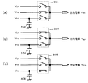
しかし、本実施の形態2で使用するOCB液晶を有する液晶パネルを完全にベンド配向にし、映像を表示するためには、液晶層に大きい電圧を印加する必要があり、対向電極の電位を大きくして液晶層に大きい電圧を印加する場合、図5の駆動回路は使用できない。したがって、図2のように対向電極の電位を切り替えることが可能な駆動回路を使用する。
【0020】
図2は実施の形態2に係る対向電極電位切り替え駆動回路である。(a)は図1のリセット期間104における対向電極電位Vscを、(b)は図1の転移期間105における対向電極電位Vgcを、(c)は図1の通常映像表示期間106におけるVncを出力する対向電極電位切り替え駆動回路の状態である。
【0021】
図2のように、各電圧をスイッチ301で切り替えることによって、図1の対向電極電位102の動作が可能になる。また、対向電極電位がVgcまたはVscになるときには、対向電極にコンデンサを付加しないようにし、Vncになるときにはコンデンサを付加するようにコンデンサ302を設置する。なぜなら、対向電極電位がVscまたはVgcになるときにスイッチ301の出力側、つまり対向電極側にコンデンサが付加していると、そのコンデンサの充放電のために所望の電位になるまでに時間がかかってしまい(波形がなまる)、リセット期間では、均一なスプレイ状態にするためのリセット期間が長く必要になり、転移期間では、液晶層をベンド配向にするための転移期間が長く必要になる。さらに、Vgcが大きいとコンデンサの充放電のために大電流が流れてしまう。また、対向電極電位Vncにコンデンサ302を付加することで、通常映像表示期間における対向電極電位を安定化し、映像表示にフリッカ、クロストーク等を抑制できる。
【0022】
なお、スイッチ301の入力側のVgcおよびVscの配線にもVncの配線と同様にコンデンサを設置しても良い。また、スイッチ301の出力側の対向電極への配線構成やパネル仕様によっては、コンデンサ302よりも比較的小さい容量のものを設置しても良い。また、本実施の形態2で使用した対向電極電位切り替え駆動回路はFETなどのスイッチング可能なもので構成することが可能である。
【0023】
本実施の形態2における駆動方式を用いると、対向電極電位の切り替え時にコンデンサの充放電による電流を低減できるので、電源回路の構成を簡素化でき、低電力化が可能である。また、より短時間で完全にパネル全体をベンド配向にすることができ、フリッカ、クロストーク等のない映像表示を提供できる。
【0024】
(実施の形態3)
図3は実施の形態3に係る対向電極電位およびゲート線電位切り替え駆動回路である。
【0025】
図3では、スイッチ401でゲート線の電位を切り替え、スイッチ402で対向電極の電位を切り替えている。また、図1の転移期間105における対向電極電位102(Vgc)をつくる電源と、ゲートドライバからゲート線に薄膜トランジスタをオンさせる電圧をつくる電源を共有している。このようにすることによって、電源回路の構成を簡略化でき、低コスト化、薄型および軽量化が可能である。ここでは、転移期間105における対向電極電位102をつくる電源と、ゲートドライバからゲート線に薄膜トランジスタをオンさせる電圧をつくる電源を共有しているが、薄膜トランジスタをオフさせる電圧が十分に小さく、液晶層に電圧を十分に印加可能であるなら、薄膜トランジスタをオフさせる電圧をつくる電源と転移期間105における対向電極電位102をつくる電源を共有してもよい。なお、対向電極切り替え駆動回路であるスイッチ402をスイッチ401と共にゲートドライバに内蔵することで、さらに低コスト化、薄型および軽量化が可能である。
【0026】
なお、以上の実施例に於いては、トランジスターをオンまたはオフさせるためのゲート線に印加する電圧を複数ラインで同時に印加ことも可能であるが、全ラインを同時に印加することも可能である。
【0027】
【発明の効果】
以上のように本発明の第1の実施形態によれば、電源投入時によって乱れた液晶層を均一なスプレイ状態にするリセット期間と、液晶層に大きい電圧を印加する転移期間を設けることにより、より短時間で完全にパネル全体をベンド配向にすることができ、より短時間で映像を表示することが可能である。
【0028】
また、本発明の第2の実施形態によれば、リセット期間および転移期間における対向電極電位を対向電極に与えるときは対向電極にコンデンサを付加せず、通常映像表示期間における対向電極電位を対向電極に与えるときは対向電極にコンデンサを付加することにより、対向電極に大電流が流れるのを防止でき、さらに短時間で完全にパネル全体をベンド配向にすることができ、フリッカ、クロストーク等のない映像表示を提供できる。
【0029】
また、本発明の第3の実施形態によれば、転移期間における対向電極電位をつくる電源と、ゲートドライバからゲート線に薄膜トランジスタをオンまたはオフさせる電圧をつくる電源を共有することにより、電源回路の構成を簡略化でき、低コスト化、薄型および軽量化が可能である。
【0030】
なお、本発明を用いれば、高速応答かつ広視野角で動画表示や大画面化に十分対応できる液晶ディスプレイを提供することができ、またブラウン管に比べ低電力であるため、地球環境、宇宙環境に優しいことになる。
【図面の簡単な説明】
【図1】本発明の第1の実施形態に係るタイムチャート
【図2】本発明の第2の実施形態に係る駆動回路図
【図3】本発明の第3の実施形態に係る駆動回路図
【図4】本発明の実施形態で用いた液晶パネルの1画素分の構成図
【図5】一般的な液晶パネルの駆動回路図
【符号の説明】
101 ゲート線電位
102 対向電極電位
103 ソース線電位
104 リセット期間
105 転移期間
106 通常映像表示期間
201,302,304,306,403 コンデンサ
301,303,305,401,402 スイッチ
501 画素トランジスタ
502 画素電極
503 Cgd(ゲート・ドレイン間容量)
504 Cst(蓄積容量)
505 Clc(液晶層の容量)
506 ソース線
507 ゲート線
508 対向電極
509 共通電極[0001]
BACKGROUND OF THE INVENTION
The present invention, ejection Dokata method and a liquid crystal panel of a liquid crystal panel Ru is transferred Oite the configured method of driving a liquid crystal panel by the liquid crystal layer, the liquid crystal layer from an initial homogeneous state at high speed bend alignment having a bend alignment The present invention relates to a liquid crystal display device by the driving method.
[0002]
[Prior art]
Liquid crystal display devices are thin and lightweight, and their use has been expanded in recent years as an alternative to conventional cathode ray tubes. However, the TN (Twisted Nematic) alignment liquid crystal panel that is widely used at present has a narrow viewing angle, a slow response speed, and the liquid crystal element is a holding type, so that it looks like a tail when displaying moving images, etc. Image quality is inferior to CRT.
[0003]
If an OCB (Optically Compensated Birefringence) liquid crystal having a bend orientation as disclosed in JP-A-61-116329 is used, it can sufficiently respond to a moving image display and a large screen with a high response speed and a wide viewing angle, and is thinner than a cathode ray tube. A large screen display with low power consumption can be provided. However, in order to transfer the OCB liquid crystal to the bend alignment, it is necessary to apply a high potential difference to the liquid crystal layer for a certain period of time. Has not reached.
[0004]
[Problems to be solved by the invention]
An object of the present invention, a liquid crystal display according Oite the driving method of a liquid crystal panel using the OCB liquid crystal, driving Dokata method and method of driving a liquid crystal panel of a liquid crystal panel you transition in a short time in the bend alignment having a bend alignment Is to provide a device .
[0005]
[Means for Solving the Problems]
In order to solve the above problems, a first invention is a thin film transistor formed in a matrix corresponding to intersections of a plurality of source lines to which pixel data is supplied and a plurality of gate lines to which a scanning signal is supplied. data, wherein a first substrate a thin film transistor connected to the image Motoden electrode and the storage capacitor element connected to the pixel electrodes are formed, opposing electrode opposed to the first substrate is formed a second substrate located between the first substrate and the second substrate, a liquid crystal layer having a bend alignment, and a source driver which drives the source over scan lines, the gate line Oite the driving method of a liquid crystal panel having a gate driver for driving,
Provided in order to bend the liquid crystal layer, the normal transition period is before video display start of the liquid crystal panel with a after power to the liquid crystal panel, the gate driver or al the Gate line wherein a voltage for turning on the thin film transistor is applied a predetermined period, and, a center value Vsc is a predetermined potential as a source line potential, the voltage of the high potential side and Vsch, the voltage on the low potential side and the Vscl AC applying a voltage from the source driver to the source line, and applies the a pair voltage greater than the AC voltage to the counter electrode Vgc, bend oriented Toe the liquid crystal layer completely,
Between the through normal image table 示期, the said gate gate driver or al the Gate line applying a voltage for turning on or off thin film transistors, the pair toward electrode simultaneously, is less voltage than said Vsc Vnc is applied,
When applying the AC voltage during the transition period, apply the Vsch and Vscl alternately and over a certain period of time,
When the storage capacitor of the storage capacitor element is Cst, the capacitance of the liquid crystal layer is Clc, the capacitance between the gate and drain of the thin film transistor is Cgd, and the variation of the gate line potential is ΔVg, the Vnc is
Vnc = Vsc−ΔVg * Cgd / (Cst + Clc + Cgd)
By using the liquid crystal panel driving method obtained in the above, the liquid crystal layer can be completely bend aligned in a shorter time, and an image can be displayed in a shorter time.
[0006]
According to the second invention, in the driving method of the first invention, since the Vgc, Vnc, and Vsc are directly driven by switching with the switching means, it is possible to prevent a large current from flowing to the counter electrode. The power consumption can be reduced. Further, the liquid crystal layer can be completely bent in a shorter time, and an image display free from flicker, crosstalk, etc. can be provided.
[0007]
The third invention is the driving method of the first aspect of the invention, the Vgc, Vnc and a first power supply that tell a Vsc, the said gate gate driver or al the Gate line thin film transistor on or off by sharing the second power that take the voltage to be, to simplify the structure of the power supply circuit, it is possible cost, thin and lightweight.
[0008]
DETAILED DESCRIPTION OF THE INVENTION
Hereinafter, embodiments of the present invention will be described with reference to FIGS. 1 to 5.
[0009]
FIG. 4 is a configuration diagram for one pixel of the liquid crystal panel used in the embodiment of the present invention.
[0010]
(Embodiment 1)
FIG. 1 is a time chart according to the first embodiment. The actual operation will be described below with reference to FIG. The source driver used here is one that can apply an AC voltage to the source line with Vsc as the center.
[0011]
A
[0012]
Here, the voltage for turning on the pixel transistor applied to each gate line should be different in timing for each gate line or for each of a plurality of gate lines. Then, the current concentration of the gate driver can be reduced and the configuration of the power supply circuit can be simplified, so that the power can be reduced.
[0013]
Next, a
[0014]
Here, the reset period and the transition period should be repeated twice or more. There may be a case where the bend alignment cannot be completely achieved at a low temperature where it is difficult to achieve bend alignment with only one reset period and transition period.
[0015]
Next, in order to display an image after the liquid crystal layer is completely bend aligned, a normal
[0016]
ΔVp = ΔVg * Cgd / (Cst + Clc + Cgd)
Here, Cst is a
[0017]
When the driving method according to the first embodiment is used, the entire panel can be completely bend-oriented in a shorter time after the power is turned on, and an image can be displayed in a shorter time.
[0018]
(Embodiment 2)
FIG. 5 shows a driving circuit of a general liquid crystal panel in which the counter electrode is a DC voltage. The counter electrode can be stably driven by adding the capacitor 201 even when the output resistance of the circuit for generating the drive voltage Vnc is high.
[0019]
However, in order to completely bend the liquid crystal panel having the OCB liquid crystal used in the second embodiment and display an image, it is necessary to apply a large voltage to the liquid crystal layer, and the potential of the counter electrode is increased. Therefore, when a large voltage is applied to the liquid crystal layer, the drive circuit of FIG. 5 cannot be used. Therefore, a driving circuit capable of switching the potential of the counter electrode as shown in FIG. 2 is used.
[0020]
FIG. 2 shows a common electrode potential switching drive circuit according to the second embodiment. (A) outputs the counter electrode potential Vsc during the
[0021]
As shown in FIG. 2, the operation of the
[0022]
Note that capacitors may be provided on the Vgc and Vsc wirings on the input side of the
[0023]
When the driving method according to the second embodiment is used, the current due to charging and discharging of the capacitor can be reduced when the counter electrode potential is switched, so that the configuration of the power supply circuit can be simplified and the power consumption can be reduced. Further, the entire panel can be completely bend-oriented in a shorter time, and an image display free from flicker, crosstalk, etc. can be provided.
[0024]
(Embodiment 3)
FIG. 3 shows a counter electrode potential and gate line potential switching drive circuit according to the third embodiment.
[0025]
In FIG. 3, the
[0026]
In the above embodiment, the voltage applied to the gate line for turning on or off the transistor can be applied simultaneously on a plurality of lines, but all the lines can be applied simultaneously.
[0027]
【The invention's effect】
As described above, according to the first embodiment of the present invention, by providing the reset period in which the liquid crystal layer disturbed by power-on is in a uniform spray state and the transition period in which a large voltage is applied to the liquid crystal layer, The entire panel can be bend-oriented completely in a shorter time, and an image can be displayed in a shorter time.
[0028]
Further, according to the second embodiment of the present invention, when applying the counter electrode potential in the reset period and the transition period to the counter electrode, no capacitor is added to the counter electrode, and the counter electrode potential in the normal video display period is set to the counter electrode. By adding a capacitor to the counter electrode, a large current can be prevented from flowing to the counter electrode, and the entire panel can be completely bend-oriented in a short time without flicker, crosstalk, etc. Can provide video display.
[0029]
Further, according to the third embodiment of the present invention, by sharing the power source for generating the counter electrode potential during the transition period and the power source for generating the voltage for turning on or off the thin film transistor from the gate driver to the gate line, The configuration can be simplified, and the cost, thickness and weight can be reduced.
[0030]
By using the present invention, it is possible to provide a liquid crystal display capable of sufficiently responding to a moving image display and a large screen with a high response speed and a wide viewing angle, and lower power compared to a cathode ray tube. It will be kind.
[Brief description of the drawings]
FIG. 1 is a time chart according to a first embodiment of the present invention. FIG. 2 is a drive circuit diagram according to a second embodiment of the present invention. FIG. 3 is a drive circuit diagram according to a third embodiment of the present invention. FIG. 4 is a block diagram of one pixel of a liquid crystal panel used in an embodiment of the present invention. FIG. 5 is a drive circuit diagram of a general liquid crystal panel.
101 Gate line potential 102
504 Cst (storage capacity)
505 Clc (capacity of liquid crystal layer)
506
Claims (12)
前記液晶層をベンド配向させるために設けられ、前記液晶パネルへの電源投入後であるとともに前記液晶パネルの通常映像表示開始前である転移期間に、前記ゲートドライバから前記ゲート線に前記薄膜トランジスタをオンさせる電圧を一定期間印加し、且つ、ソース線電位として所定の電位であるVscを中心値とし、高電位側の電圧をVschとし、低電位側の電圧をVsclとした交流電圧を前記ソースドライバから前記ソース線に印加し、且つ、前記対向電極に前記交流電圧より大きい電圧であるVgcを印加し、前記液晶層を完全にベンド配向させ、
前記通常映像表示期間に、前記ゲートドライバから前記ゲート線に前記薄膜トランジスタをオンまたはオフさせる電圧を印加し、同時に前記対向電極に、前記Vscよりも小さい電圧であるVncを印加し、
前記転移期間に前記交流電圧を印加する際、前記VschおよびVsclを交番且つ一定期間にわたり印加し、
前記蓄積容量素子の蓄積容量をCst、前記液晶層の容量をClc、前記薄膜トランジスタのゲート・ドレイン間の容量をCgd、前記ゲート線電位の変動分をΔVgとすると、前記Vncは、
Vnc=Vsc−ΔVg*Cgd/(Cst+Clc+Cgd)
で得られることを特徴とする液晶パネルの駆動方法。A plurality of source lines to which pixel data are supplied, to correspond to the intersection of the plurality of gate lines when the scan signals are supplied, a thin film was formed in a matrix transistors data, before Symbol fraction is connected to the thin film transistor Motoden A first substrate on which a storage capacitor element connected to the electrode and the pixel electrode is formed; a second substrate on which a counter electrode facing the first substrate is formed; the first substrate and the first substrate; located between the second substrate, a liquid crystal layer having a bend alignment, and a source driver which drives the source line, Oite the driving method of a liquid crystal panel having a gate driver for driving the gate lines,
Provided in order to bend alignment liquid crystal layer, the normal transition period is before video display start of the liquid crystal panel with a after power to the liquid crystal panel, the thin film transistor to the gate line from the previous SL gate driver The source driver applies an alternating voltage in which a voltage to be turned on is applied for a certain period , Vsc, which is a predetermined potential as a source line potential, has a center value, Vsch is a high potential side voltage, and Vscl is a low potential side voltage. wherein is applied to the source line, and, by applying a pre-SL is a voltage greater than the AC voltage to the common electrode Vgc, Toe bend oriented said liquid crystal layer completely from
Between the through normal image table 示期, the voltage to be pre SL on or off the thin film transistor to the gate lines from the gate driver applies the counter electrode, and applying the a smaller voltage than Vsc Vnc simultaneously,
When applying the AC voltage during the transition period, apply the Vsch and Vscl alternately and over a certain period of time,
When the storage capacitor of the storage capacitor element is Cst, the capacitance of the liquid crystal layer is Clc, the capacitance between the gate and drain of the thin film transistor is Cgd, and the variation of the gate line potential is ΔVg, the Vnc is
Vnc = Vsc−ΔVg * Cgd / (Cst + Clc + Cgd)
A method for driving a liquid crystal panel obtained by
前記第1のリセット電圧および第2のリセット電圧の電位差を±1V以内に設定することを特徴とする請求項1から6のいずれかに記載の液晶パネルの駆動方法。 The reset period is before the transition period as well as a post-power supply to the liquid crystal panel, a voltage for turning on the thin film transistor to the gate line from the previous SL gate driver applies, with a predetermined potential to the counter electrode at the same time a first reset voltage is applied, applying a second reset voltage having a further predetermined potential to said source line simultaneously from previous SL source driver,
It said first reset voltage and a second driving method of a liquid crystal panel according to any one of claims 1 to 6 the potential of the reset voltage, characterized in that you set within ± 1V.
Priority Applications (1)
| Application Number | Priority Date | Filing Date | Title |
|---|---|---|---|
| JP2001321669A JP3967577B2 (en) | 2001-10-19 | 2001-10-19 | Method for driving liquid crystal panel and liquid crystal display device |
Applications Claiming Priority (1)
| Application Number | Priority Date | Filing Date | Title |
|---|---|---|---|
| JP2001321669A JP3967577B2 (en) | 2001-10-19 | 2001-10-19 | Method for driving liquid crystal panel and liquid crystal display device |
Publications (2)
| Publication Number | Publication Date |
|---|---|
| JP2003121881A JP2003121881A (en) | 2003-04-23 |
| JP3967577B2 true JP3967577B2 (en) | 2007-08-29 |
Family
ID=19138851
Family Applications (1)
| Application Number | Title | Priority Date | Filing Date |
|---|---|---|---|
| JP2001321669A Expired - Fee Related JP3967577B2 (en) | 2001-10-19 | 2001-10-19 | Method for driving liquid crystal panel and liquid crystal display device |
Country Status (1)
| Country | Link |
|---|---|
| JP (1) | JP3967577B2 (en) |
Families Citing this family (13)
| Publication number | Priority date | Publication date | Assignee | Title |
|---|---|---|---|---|
| JP4671588B2 (en) | 2003-08-11 | 2011-04-20 | 株式会社日立製作所 | Projection optical unit, projection color image display device, and rear projection color image display device using the same |
| JP4484137B2 (en) * | 2004-02-13 | 2010-06-16 | シャープ株式会社 | Active matrix display device, driving method thereof, and electronic information device |
| WO2005081052A1 (en) | 2004-02-20 | 2005-09-01 | Toshiba Matsushita Display Technology Co., Ltd. | Liquid crystal display device |
| JP4528775B2 (en) | 2004-02-20 | 2010-08-18 | 東芝モバイルディスプレイ株式会社 | Liquid crystal display |
| JP4679219B2 (en) * | 2004-04-15 | 2011-04-27 | 東芝モバイルディスプレイ株式会社 | Liquid crystal panel drive device, liquid crystal display device |
| JP4775057B2 (en) * | 2005-04-27 | 2011-09-21 | セイコーエプソン株式会社 | Liquid crystal device, driving method thereof, and electronic apparatus |
| JP2007072270A (en) * | 2005-09-08 | 2007-03-22 | Toshiba Matsushita Display Technology Co Ltd | Liquid crystal display and method for driving liquid crystal display |
| JP2007206415A (en) * | 2006-02-02 | 2007-08-16 | Toshiba Matsushita Display Technology Co Ltd | Counter voltage output device and liquid crystal display |
| KR101189090B1 (en) * | 2006-07-18 | 2012-11-09 | 삼성디스플레이 주식회사 | Liquid crystal display apparatus and mathod of driving thereof |
| US7986378B2 (en) | 2006-09-20 | 2011-07-26 | Sharp Kabushiki Kaisha | Liquid crystal display device, its drive method, liquid crystal panel drive device, and liquid crystal panel drive method |
| JP2008250223A (en) * | 2007-03-30 | 2008-10-16 | Casio Comput Co Ltd | Liquid crystal display device |
| WO2009031391A1 (en) | 2007-09-07 | 2009-03-12 | Sharp Kabushiki Kaisha | Method for driving liquid crystal display device and liquid crystal display device |
| US8436954B2 (en) | 2007-09-07 | 2013-05-07 | Sharp Kabushiki Kaisha | Method of driving liquid crystal display device, and liquid crystal display device |
-
2001
- 2001-10-19 JP JP2001321669A patent/JP3967577B2/en not_active Expired - Fee Related
Also Published As
| Publication number | Publication date |
|---|---|
| JP2003121881A (en) | 2003-04-23 |
Similar Documents
| Publication | Publication Date | Title |
|---|---|---|
| US20090009459A1 (en) | Display Device and Method for Driving Same | |
| JP3240367B2 (en) | Active matrix type liquid crystal image display | |
| JP2002091403A (en) | Liquid crystal panel driving method of dot inversion system and its device | |
| JP2002055325A (en) | Liquid crystal display device using swing common electrode and its driving method | |
| JP2001282205A (en) | Active matrix type liquid crystal display device and method for driving the same | |
| WO2006049245A1 (en) | Liquid crystal display apparatus and method for driving the same | |
| JP2001215469A (en) | Liquid crystal display device | |
| JP3967577B2 (en) | Method for driving liquid crystal panel and liquid crystal display device | |
| US7791578B2 (en) | Circuit for driving common voltage of in-plane switching mode liquid crystal display device | |
| JPH09134152A (en) | Liquid-crystal display device | |
| JP2011221564A (en) | Liquid crystal device | |
| JP2003202546A (en) | Driving method and device for liquid crystal display device | |
| JP2007241029A (en) | Liquid crystal display | |
| US7868962B2 (en) | Pixel circuit, pixel array and method for discharging a capacitor unit of the pixel circuit | |
| JP2006053428A (en) | Gate line driving circuit | |
| JP2006058638A (en) | Gate line driving circuit | |
| JP3914639B2 (en) | Liquid crystal display | |
| JP2004258139A (en) | Liquid crystal display device | |
| JP3182350B2 (en) | Driving method of liquid crystal display | |
| JPH09243995A (en) | Active matrix array, liquid crystal display device and its drive method | |
| JP2005128153A (en) | Liquid crystal display apparatus and driving circuit and method of the same | |
| JP3193462B2 (en) | Driving method of active matrix type thin film transistor liquid crystal panel | |
| JP2000020033A (en) | Liquid crystal display device | |
| JP2006047848A (en) | Gate line driving circuit | |
| US6812910B2 (en) | Driving method for liquid crystal display |
Legal Events
| Date | Code | Title | Description |
|---|---|---|---|
| A621 | Written request for application examination |
Free format text: JAPANESE INTERMEDIATE CODE: A621 Effective date: 20041007 |
|
| RD01 | Notification of change of attorney |
Free format text: JAPANESE INTERMEDIATE CODE: A7421 Effective date: 20050701 |
|
| A711 | Notification of change in applicant |
Free format text: JAPANESE INTERMEDIATE CODE: A711 Effective date: 20061109 |
|
| A977 | Report on retrieval |
Free format text: JAPANESE INTERMEDIATE CODE: A971007 Effective date: 20070111 |
|
| A131 | Notification of reasons for refusal |
Free format text: JAPANESE INTERMEDIATE CODE: A131 Effective date: 20070306 |
|
| A521 | Written amendment |
Free format text: JAPANESE INTERMEDIATE CODE: A523 Effective date: 20070427 |
|
| TRDD | Decision of grant or rejection written | ||
| A01 | Written decision to grant a patent or to grant a registration (utility model) |
Free format text: JAPANESE INTERMEDIATE CODE: A01 Effective date: 20070529 |
|
| A61 | First payment of annual fees (during grant procedure) |
Free format text: JAPANESE INTERMEDIATE CODE: A61 Effective date: 20070531 |
|
| R150 | Certificate of patent or registration of utility model |
Free format text: JAPANESE INTERMEDIATE CODE: R150 |
|
| S533 | Written request for registration of change of name |
Free format text: JAPANESE INTERMEDIATE CODE: R313533 |
|
| FPAY | Renewal fee payment (event date is renewal date of database) |
Free format text: PAYMENT UNTIL: 20100608 Year of fee payment: 3 |
|
| R350 | Written notification of registration of transfer |
Free format text: JAPANESE INTERMEDIATE CODE: R350 |
|
| FPAY | Renewal fee payment (event date is renewal date of database) |
Free format text: PAYMENT UNTIL: 20100608 Year of fee payment: 3 |
|
| FPAY | Renewal fee payment (event date is renewal date of database) |
Free format text: PAYMENT UNTIL: 20110608 Year of fee payment: 4 |
|
| FPAY | Renewal fee payment (event date is renewal date of database) |
Free format text: PAYMENT UNTIL: 20120608 Year of fee payment: 5 |
|
| S531 | Written request for registration of change of domicile |
Free format text: JAPANESE INTERMEDIATE CODE: R313531 |
|
| FPAY | Renewal fee payment (event date is renewal date of database) |
Free format text: PAYMENT UNTIL: 20120608 Year of fee payment: 5 |
|
| R350 | Written notification of registration of transfer |
Free format text: JAPANESE INTERMEDIATE CODE: R350 |
|
| FPAY | Renewal fee payment (event date is renewal date of database) |
Free format text: PAYMENT UNTIL: 20120608 Year of fee payment: 5 |
|
| FPAY | Renewal fee payment (event date is renewal date of database) |
Free format text: PAYMENT UNTIL: 20130608 Year of fee payment: 6 |
|
| S533 | Written request for registration of change of name |
Free format text: JAPANESE INTERMEDIATE CODE: R313533 |
|
| FPAY | Renewal fee payment (event date is renewal date of database) |
Free format text: PAYMENT UNTIL: 20130608 Year of fee payment: 6 |
|
| R350 | Written notification of registration of transfer |
Free format text: JAPANESE INTERMEDIATE CODE: R350 |
|
| FPAY | Renewal fee payment (event date is renewal date of database) |
Free format text: PAYMENT UNTIL: 20140608 Year of fee payment: 7 |
|
| R250 | Receipt of annual fees |
Free format text: JAPANESE INTERMEDIATE CODE: R250 |
|
| R250 | Receipt of annual fees |
Free format text: JAPANESE INTERMEDIATE CODE: R250 |
|
| LAPS | Cancellation because of no payment of annual fees |