JP3948292B2 - Semiconductor memory device and manufacturing method thereof - Google Patents
Semiconductor memory device and manufacturing method thereof Download PDFInfo
- Publication number
- JP3948292B2 JP3948292B2 JP2002024918A JP2002024918A JP3948292B2 JP 3948292 B2 JP3948292 B2 JP 3948292B2 JP 2002024918 A JP2002024918 A JP 2002024918A JP 2002024918 A JP2002024918 A JP 2002024918A JP 3948292 B2 JP3948292 B2 JP 3948292B2
- Authority
- JP
- Japan
- Prior art keywords
- film
- forming
- memory device
- semiconductor memory
- wiring
- Prior art date
- Legal status (The legal status is an assumption and is not a legal conclusion. Google has not performed a legal analysis and makes no representation as to the accuracy of the status listed.)
- Expired - Fee Related
Links
Images


Classifications
-
- H—ELECTRICITY
- H10—SEMICONDUCTOR DEVICES; ELECTRIC SOLID-STATE DEVICES NOT OTHERWISE PROVIDED FOR
- H10B—ELECTRONIC MEMORY DEVICES
- H10B63/00—Resistance change memory devices, e.g. resistive RAM [ReRAM] devices
- H10B63/30—Resistance change memory devices, e.g. resistive RAM [ReRAM] devices comprising selection components having three or more electrodes, e.g. transistors
- H10B63/34—Resistance change memory devices, e.g. resistive RAM [ReRAM] devices comprising selection components having three or more electrodes, e.g. transistors of the vertical channel field-effect transistor type
-
- H—ELECTRICITY
- H10—SEMICONDUCTOR DEVICES; ELECTRIC SOLID-STATE DEVICES NOT OTHERWISE PROVIDED FOR
- H10B—ELECTRONIC MEMORY DEVICES
- H10B63/00—Resistance change memory devices, e.g. resistive RAM [ReRAM] devices
- H10B63/80—Arrangements comprising multiple bistable or multi-stable switching components of the same type on a plane parallel to the substrate, e.g. cross-point arrays
-
- G—PHYSICS
- G11—INFORMATION STORAGE
- G11C—STATIC STORES
- G11C13/00—Digital stores characterised by the use of storage elements not covered by groups G11C11/00, G11C23/00, or G11C25/00
- G11C13/0002—Digital stores characterised by the use of storage elements not covered by groups G11C11/00, G11C23/00, or G11C25/00 using resistive RAM [RRAM] elements
- G11C13/0004—Digital stores characterised by the use of storage elements not covered by groups G11C11/00, G11C23/00, or G11C25/00 using resistive RAM [RRAM] elements comprising amorphous/crystalline phase transition cells
-
- G—PHYSICS
- G11—INFORMATION STORAGE
- G11C—STATIC STORES
- G11C2213/00—Indexing scheme relating to G11C13/00 for features not covered by this group
- G11C2213/70—Resistive array aspects
- G11C2213/79—Array wherein the access device being a transistor
-
- H—ELECTRICITY
- H10—SEMICONDUCTOR DEVICES; ELECTRIC SOLID-STATE DEVICES NOT OTHERWISE PROVIDED FOR
- H10N—ELECTRIC SOLID-STATE DEVICES NOT OTHERWISE PROVIDED FOR
- H10N70/00—Solid-state devices without a potential-jump barrier or surface barrier, and specially adapted for rectifying, amplifying, oscillating or switching
- H10N70/20—Multistable switching devices, e.g. memristors
- H10N70/231—Multistable switching devices, e.g. memristors based on solid-state phase change, e.g. between amorphous and crystalline phases, Ovshinsky effect
-
- H—ELECTRICITY
- H10—SEMICONDUCTOR DEVICES; ELECTRIC SOLID-STATE DEVICES NOT OTHERWISE PROVIDED FOR
- H10N—ELECTRIC SOLID-STATE DEVICES NOT OTHERWISE PROVIDED FOR
- H10N70/00—Solid-state devices without a potential-jump barrier or surface barrier, and specially adapted for rectifying, amplifying, oscillating or switching
- H10N70/801—Constructional details of multistable switching devices
- H10N70/821—Device geometry
- H10N70/826—Device geometry adapted for essentially vertical current flow, e.g. sandwich or pillar type devices
-
- H—ELECTRICITY
- H10—SEMICONDUCTOR DEVICES; ELECTRIC SOLID-STATE DEVICES NOT OTHERWISE PROVIDED FOR
- H10N—ELECTRIC SOLID-STATE DEVICES NOT OTHERWISE PROVIDED FOR
- H10N70/00—Solid-state devices without a potential-jump barrier or surface barrier, and specially adapted for rectifying, amplifying, oscillating or switching
- H10N70/801—Constructional details of multistable switching devices
- H10N70/881—Switching materials
- H10N70/882—Compounds of sulfur, selenium or tellurium, e.g. chalcogenides
- H10N70/8828—Tellurides, e.g. GeSbTe
Description
【0001】
【発明の属する技術分野】
本発明は、半導体記憶装置に関する。特に、低電圧で動作する、高速かつ不揮発性を有する、ランダムアクセスメモリ(RAM)に関する。
【0002】
【従来の技術】
携帯電話に代表されるモバイル機器の需要に牽引されて、不揮発メモリの市場の伸びは著しい。その代表が、FLASHメモリであるが、本質的に速度が遅いために、プログラマブルなROMとして用いられている。一方、作業用のメモリとしては、高速なDRAMが必要であり、携帯機器用メモリとしては、FLASHとDRAMの両方が搭載されている。これら2つのメモリの特長を具備した素子が実現できれば、FLASHとDRAMを1チップ化することが可能となるばかりでなく、すべての半導体メモリを置き換えることになるという点で、そのインパクトは極めて大きい。こうしたメモリの1つとして、2001 IEDM(International Electron Device Meeting)において、相変化を利用したメモリ(OUM:Ovonic Unified Memory)がIntelより提案された。
次にこのメモリの動作原理を簡単に説明する。OUMは、結晶状態により抵抗値が異なるカルコゲナイドという材料を記憶ノードとして用いる。カルコゲナイドはDVDやCDの媒体に用いられている材料であり、少なくともアンチモン(Sb)とテルル(Te)を含むGe−Sb−Te系やAg−In−Sb−Te系などがその代表である。基本的なメモリセルは、選択トランジスタとカルコゲナイドから構成されており、所謂DRAMセルと類似しており、キャパシタをカルコゲナイドに置き換えたものとみなすことができる。カルコゲナイドは、その結晶状態が単結晶かアモルファスかで、その抵抗値が10〜10000倍程度異なる。この違いを利用して、固体メモリにするものである。不揮発メモリとして注目をあびているMRAM(Magnetic RAM)の場合、抵抗の変化率は40%程度であるので、OUMの方がはるかに大きく、データのセンシングが容易である。
カルコゲナイドの結晶状態を変える為には電圧を印加することにより発生するジュール熱を利用する。アモルファス化する際には、カルコゲナイドを600℃程度に加熱し溶解させ、急冷する。結晶化する際には、400℃程度の温度で50nsec程度保持する。従って、データの書き込みには図2に示すようなパルスを与えることになる。読出しの際には、ワード線をオンにし、共通グラウンド線とビット線)間を流れる電流により、2値の情報(”0”,”1”)を判別する。
【0003】
【発明が解決しようとする課題】
上で述べた、選択トランジスタとカルコゲナイドから構成される相変化メモリは、そのセル面積は8F2程度以上である。ここで、Fは最小加工寸法である。大容量化のためには、さらなるメモリセル面積の縮小が課題である。
【0004】
【課題を解決するための手段】
上記課題を解決する為に、縦型トランジスタを用いたメモリセル構造及びその製造方法を提案する。本発明によれば、面積4F2のメモリセルが実現できる。本発明による、メモリセル構造の代表的なものを図1に示す。下から順に、書き込み及び読み出しのための第1の配線(7)、この配線と電気的に接続された縦型の選択トランジスタ(1)、その上に情報を蓄えるカルコゲナイド材料(2)、その上に書き込み及び読み出しのための第2の配線(8)、の構成となっている。本発明におけるメモリセルの平面レイアウトを図3に示す。セル配線(803)とワード線(403)が最小ピッチ2Fで配置されるので、メモリセルの面積は4F2となる。
【0005】
【発明の実施の形態】
(実施例1)
本実施例では、図1に示したメモリセルの製造方法を、その製造工程をたどりながら詳細に説明する。本発明によれば、図1に示した第1の配線(7)及び第2の配線(8)を、それぞれ分離することが可能であり、メモリセル動作の自由度を広げるという特長がある。
まず始めに、通常の製造方法により、周辺回路用のCMOSトランジスタを形成する。その上に、図4に示すように、層間絶縁膜(9)を堆積し平坦化した後に、メモリセル領域においてはピッチが0.2ミクロンの第1のセル配線(701)を、周辺回路領域においては、ローカルインターコネクト線を形成する。本実施例においては、配線材料としてはタングステンまたはW90Ti10などのタングステン合金を用いた。勿論、タングステンまたはW90Ti10などのタングステン合金の変わりに、不純物を高濃度含む多結晶シリコンや、多結晶シリコンと金属あるいはシリサイドとの積層膜でも構わない。
さらに、層間絶縁膜(901)を100nm堆積し、不純物としてリンを1E20/cm2程度の高濃度に含むポリシリプラグ(10)を形成し、図5のようになる。このプラグにより、後に、セル配線(701)と選択トランジスタが電気的に接続される。勿論多結晶シリコンの代わりに金属あるいは、シリサイドを用いることも可能である。
【0006】
次に、縦型トランジスタを形成する。ここでは、以下の順に膜を堆積する。まず、縦型トランジスタの拡散層となる不純物としてリンを1E20/cm2程度の高濃度にドープしたN+層(502)、チャネル部となる不純物としてボロンを1E16/cm2程度の濃度で含む不純物層(602)、更に拡散層となる不純物としてリンを1E20/cm2程度の高濃度にドープしたN+層(503)、を堆積する。これらがトランジスタ部となる。ここで、不純物拡散層(502及び503)からの、チャネル部(602)への、不純物の拡散を抑えるために、厚さ1nm程度の絶縁膜を、チャネル部(602)と拡散層(502及び503)の間に挟んでも構わない。絶縁膜としては、シリコン酸化膜やシリコンチッカ膜等が適用可能である。この後、シリコンの結晶性を改善するために熱処理を施す。もちろん、この際、レーザーアニール等の手法を用いることにより、更に良好な結晶を形成することも可能である。この場合、トランジスタの性能が向上することは言うまでも無い。さらに、後に施す層間膜平坦化工程(CMP:Chemical Mechanical Polishing)のストッパ膜として、シリコン窒化膜(11)を100nm堆積する。この積層膜を、図6に示すように、ピッチ0.2ミクロンのラインアンドスペース状に加工する。
引き続き、層間絶縁膜(902)を堆積し、CMPにより平坦化、さらに加工用に用いたシリコン窒化膜を除去することにより、下地の多結晶シリコン(503)を露出させる。この時の状態を図7に示す。
【0007】
次に膜厚50nmのカルコゲナイド材料(202)と第2のセル配線(802)となる膜厚100nmのタングステンまたはW90Ti10などのタングステン合金、及び厚さ100nmの酸化膜(903)を堆積する。この際、カルコゲナイド材料(202)の多結晶シリコン(503)への拡散を防止する目的で、多結晶シリコン(503)との間にTiAlN等の遷移金属の窒化物や酸化物等のバリア膜や、W80Ti20などの金属導電膜、あるいはこれらの積層膜を堆積すれば、書換え可能回数が増大する利点が有る。あるいは、カルコゲナイドの相状態を変えるのに必要な熱の拡散を抑制する目的で、例えば、ITO(インジウムとスズの酸化物の混合物)のような熱伝導率の悪い導電膜を間に挟むことも、勿論可能である。続いて、図8に示すように、先に形成した第1の配線(701)と垂直方向に、0.2ミクロンピッチのラインアンドスペース状に加工する。尚、本実施例においては、第2のセル配線(802)間の容量を低減する目的で、線幅の細線化を行った。具体的には、レジストパタンの露光後に、軽度のアッシングプロセスを施し、レジスト寸法を70nmに細線化した。
【0008】
次に、選択トランジスタのワード線の形成を行う。まず、ワード線と第2の配線(802)との短絡を防ぐ目的で、図9に示すように、膜厚30nmの側壁酸化膜(904)を形成する。この工程により、カルコゲナイド(202)は、第2の配線(802)と側壁酸化膜(904)等により、完全に覆われる。さらに、酸化膜で覆われた第2の配線(802)をマスクに、自己整合的に、下地の多結晶シリコンの積層膜をエッチングし、図10のようになる。
続いて、低温で形成が可能なCVD法により10nmの膜厚のゲート酸化膜を形成する。この際、カルコゲナイドが上記のように、完全に覆われているので、昇華することはない。従って、より高温プロセスである熱酸化によるゲート酸化も可能である。本実施例においては、更にはワード線となるタングステンまたはW90Ti10などのタングステン合金(12)を堆積/平坦化し、図11のようになる。本実施例においては、タングステンまたはW90Ti10などのタングステン合金を用いたが、間にバリアメタルを挟んだタングステンまたはW90Ti10などのタングステン合金と多結晶シリコンの積層膜や、ポリサイド等を用いても勿論構わない。次に、通常のドライエッチ法により、タングステンまたはW90Ti10などのタングステン合金を、第2のセル配線(802)と垂直方向に走る、ピッチ0.2ミクロンのラインアンドスペース状に加工する。この時の状態を図12に示す。ワード線(402)加工の際、電極材料を平坦化した結果として、エッチング段差は第2のセル配線(802)の高さとキャップ酸化膜(903)をあわせた高さとなる。このように、本実施例の場合、選択トランジスタは、ゲート電極(402)がチャネル部を両側からはさみこんだダブルゲート構造になる。この結果、トランジスタは完全空乏型SOI(Silicon On Insulator)として動作し、良好なスイッチング特性を実現する。
最後に、必要な多層金属配線層を形成し、所望の半導体装置を得ることができる。本実施例においては、縦型トランジスタを用いることにより、従来DRAMの約半分のセル面積を有する半導体記憶装置を実現できる。
【0009】
(実施例2)
実施例1においては、第1の配線(701)をワード線(402)毎に分離する構造としたが、本実施例はこの第1の配線(702)を分離加工しないメモリセルに関するものである。セルの構造を図13に示す。製造方法は実施例1とほぼ同様である。本実施例の場合、第1の配線(702)の電位が安定するという効果がある。
【0010】
(実施例3)
実施例1においては、第1の配線(701)と第2の配線(802)が互いに直交する構成としたが、お互いに並行になるような構成が可能なことは明らかである。メモリセルの構造を図14に示す。製造方法は実施例1とほぼ同様である。この場合、第1と第2のメモリセル配線をペアとし、このペア線とワード線でメモリセルを選択することが可能になる。
【0011】
(実施例4)
実施例1〜3においては、カルコゲナイド材料製膜後に、ゲート酸化膜が形成されるため、カルコゲナイドが高温にさらされるという問題がある。実施例1で述べたように、電極等で完全に覆われていれば問題はないが、わずかながら体積変化するので、カルコゲナイドに対し、高温プロセスを行なうことは避けた方が望ましい。
この目的のため、本実施例においてはゲート酸化膜形成後に、カルコゲナイドを形成することとした。本実施例におけるメモリセルレイアウトを図15に示す。後に説明するが、自己整合的にワード線を形成するために、横方向(A−A)と縦方向(B−B)とでセル配置のピッチが異なっている。図15においては、最小加工寸法をFとした時に、横方向(A−A)は最小ピッチである2F、縦方向(B−B)は3Fとした。すなわち、セル面積は6F2である。もちろん、このレイアウトは任意に設定可能であり、本発明が面積6F2のメモリセルに限るものでないことは、いうまでもない。
【0012】
図5に示す工程まで、実施例1と同様な製造工程を行う。続いて、縦型トランジスタの拡散層となる不純物を高濃度にドープしたN+層(504)、チャネル部となる低濃度不純物層(603)、更に拡散層となるN+層(505)、を堆積し、アニール工程により結晶化した。次に、通常のドライエッチング工程により、図16に示すようにメモリセル毎に分離し、更に、10nmのゲート酸化膜をCVD法により堆積した。もちろん、ゲート酸化膜形成は熱酸化工程でも構わない。その後、通常のCVD法により、高濃度に不純物をふくんだ多結晶シリコンを堆積し、ドライエッチングプロセスにより、側壁ゲート電極を形成する。この時の図15における(A−A)及び(B−B)方向の断面図をそれぞれ図17、18に示す。すなわち、メモリセルのピッチが異なるので、自己整合的に、(A−A)方向では側壁ワード電極がつながり、(B−B)方向では分離した構造になる。本実施例においては、自己整合的にワード線を分離する手法を用いたが、レジストマスク等を用いた通常のドライエッチ法により形成することも可能である。
続いて、公知のCVD法により1ミクロン程度の酸化膜を堆積し、公知のCMP法による平坦化を行い、コンタクトを開口し、下地の多結晶シリコンを露出させて、断面図は図19のようになる。続いて、酸化膜を30nm程度堆積させ、ドライエッチングによりエッチバックを行ない、側壁酸化膜(906)を形成し、図20のようになる。このように、自己整合的にコンタクト寸法を縮めた理由は次の通りである。カルコゲナイドの相状態を変える為には、熱を与える必要がある。効率良くカルコゲナイドの温度を上昇させるためには、カルコゲナイドの抵抗をある程度大きくする必要がある。これは、低電圧動作をさせるという観点からも重要である。この目的のためには、選択トランジスタの拡散層とカルコゲナイド接触面積を低減することが効果的である。こうした理由から、自己整合的にコンタクト寸法を縮める手段をとった。
【0013】
続いて、カルコゲナイド材料(203)及び、第2のセル配線(803)となるタングステンまたはW90Ti10などのタングステン合金を堆積し、図21のようになる。カルコゲナイド材料積層前にTiAlN等の遷移金属の窒化物や酸化物等のバリア膜や、W80Ti20 などの金属導電膜、あるいはこれらの積層膜を堆積すれば、書換え可能回数が増大する利点が有る。あるいは、カルコゲナイドの相状態を変えるのに必要な熱の拡散を抑制する目的で、例えば、ITO(インジウムとスズの酸化物の混合物)のような熱伝導率の悪い導電膜を間に挟むことも、勿論可能である。メモリセルに関しては、図21のままでも動作する。すなわち第2の配線(803)が共通線となり、第1の配線(701)がデータ線となる。この場合、カルコゲナイドを加工しないで済むという特長がある。更には、相状態を変える際に発生する熱を、平面状に形成された第2の配線(803)を通して、効果的に逃がすことが可能になり、熱履歴の影響を排除する結果として動作が安定する。また、メモリセル動作としては、第2の配線(803)を一枚板とすることにより、電位が安定するという効果がある。
もちろん、第2の配線(803)を分離することも可能である。その際、タングステンまたはW90Ti10などのタングステン合金を通常のドライエッチング法により、第1のセル配線と並行方向に分離し、図22のようになる。
最後に、必要な多層金属配線を形成し、所望の半導体記憶装置を得る。
【0014】
(実施例5)
実施例4において、選択トランジスタとカルコゲナイドの接触面積を低減することが、低電圧動作をさせるのに有効であることを述べた。これは、実施例1〜3に述べた構造に対しても適用可能である。以下、その実現方法を図面を用いて説明する。
図6までは、実施例1と同様な製造工程を行なう。続いて、層間絶縁膜(902)を堆積し、CMPにより平坦化し、下地のシリコン窒化膜を露出させて図23のようになる。さらに、熱リン酸によるウエット処理によりシリコン窒化膜を除去し、通常のCVD法により、30nmのシリコン酸化膜を堆積し、エッチバックプロセスにより側壁酸化膜(907)を形成し、図24のようになる。このように、自己整合的にコンタクトの寸法を縮めた。本実施例においては、側壁膜を通常のシリコン酸化膜により形成したが、熱伝導率の悪いポーラス状の酸化膜等を用いることも可能である。この場合、カルコゲナイドの相状態を変えるのに必要な熱の拡散を防ぐことができるので、更に効率良く、相状態を変えることが可能になる。同様な目的に適した材料としてゲルマニウムオキサイド(GeO2)も適用できる。
続いて、カルコゲナイド材料(204)及び、第2のセル配線(804)となるタングステンまたはW90Ti10などのタングステン合金、さらには及び酸化膜(908)を堆積して、図25のようになる。カルコゲナイド材料積層前にTiAlN等の遷移金属の窒化物や酸化物等のバリア膜や、W80Ti20などの金属導電膜、あるいはこれらの積層膜を堆積すれば、書換え可能回数が増大する利点が有る。あるいは、カルコゲナイドの相状態を変えるのに必要な熱の拡散を抑制する目的で、例えば、ITO(インジウムとスズの酸化物の混合物)のような熱伝導率の悪い導電膜を間に挟むことも、勿論可能である。以降は、実施例1における図8から図12までと同様な製造工程を経て、更には必要な多層金属配線を形成し、所望の半導体装置を得る。
【0015】
(実施例6)
これまでの実施例においては、プロセスの簡易性から、選択トランジスタを多結晶シリコンにより形成したが、勿論、シリコン基板中に形成することも可能である。この場合、多結晶からなるトランジスタよりも良好な特性を実現するという特長がある。本実施例においては、エピタキシャル成長したシリコン基板を用いた。以下、図面を用いて製造方法を説明する。
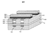
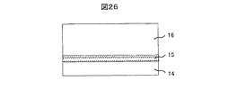
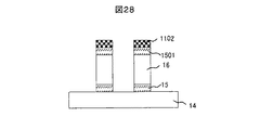
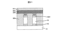
p型半導体基板を用意して、アンチモン(Sb)を1E20/cm2のドーズ量で打ち込み、エピタキシャル成長させる。勿論、アンチモンの代わりにヒソ(As)やリン(P)を用いることも可能である。この結果、図26に示すような高濃度N型不純物層(15)が内部に形成された基板ができる。高濃度N型不純物層(15)は選択トランジスタの拡散層となる。続いて、ヒ素を1E20/cm2のドーズ量で注入し、アニール工程により活性化する。これが、選択トランジスタのもう1つの拡散層となる。さらに、後で施す層間膜平坦化工程(CMP:Chemical Mechanical Polishing)のストッパ膜として、シリコン窒化膜(1102)を100nm堆積して、図27のようになる。次に図28に示すように、通常のドライエッチングプロセスにより、0.2ミクロンピッチのラインアンドスペース状に、埋め込まれた不純物拡散層(15)まで掘り、柱状に分離する。この工程は実施例1における図6と同様である。引き続き、層間絶縁膜(909)を堆積し、CMPにより平坦化、さらに加工用に用いたシリコン窒化膜(1102)を露出して図29のようになる。ついで、シリコン窒化膜(1102)を除去し、下地の不純物拡散層(1501)を露出させる。さらには、選択トランジスタの拡散層とカルコゲナイドの接触面積を低減するために、酸化膜を30nm程度堆積させ、ドライエッチングによりエッチバックを行ない、側壁酸化膜(910)を形成し、図30のようになる。続いて、カルコゲナイド材料(205)及び、第2のセル配線(805)となるタングステンまたはW90Ti10などのタングステン合金、さらには酸化膜(911)を堆積して、図31のようになる。
【0016】
カルコゲナイド材料積層前にTiAlN等の遷移金属の窒化物や酸化物等のバリア膜や、W80Ti20などの金属導電膜、あるいはこれらの積層膜を堆積すれば、書換え可能回数が増大する利点が有る。あるいは、カルコゲナイドの相状態を変えるのに必要な熱の拡散を抑制する目的で、例えば、ITO(インジウムとスズの酸化物の混合物)のような熱伝導率の悪い導電膜を間に挟むことも、勿論可能である。続いて、通常のドライエッチング工程により、図28で形成したパターンと垂直方向に、酸化膜(911)、第2のセル配線(805)、カルコゲナイド材料(205)、の積層膜をラインアンドスペース状に加工する。さらに、第2のセル配線(805)と後に形成するワード線との短絡を防ぐ為に酸化膜を30nm堆積し、エッチバックプロセスにより、側壁酸化膜(912)を形成する。続けて、ドライエッチングにより、下地の不純物拡散層(1501)とエピタキシャル成長部分(16)まで完全に分離し、不純物拡散層(15)の途中で加工を止め、図32のようになる。尚、図32は第2のセル配線(805)に垂直な方向の断面図を示している。以降は実施例1の図11から図12に示す製造工程を経て、最後に多層金属配線層を形成し、所望の半導体記憶装置を得る。
【0017】
また本発明においては、さらに、図33に等価回路を示す本発明によるメモリセルを用いれば、図34に示すようなメモリアレイを構成することができる。本アレイにおいては、データ線に相当する第2のセル配線(806)に平行な、ソース線に相当する第1のセル選択線(704)が設けられ、メモリセル内の選択トランジスタのソースが対応するソース線に接続された構成とすることにより、読み出し動作における消費電力を低減することができる。具体的には、選択したいデータ線(たとえばDL1)に対応するソース線(たとえばSL1)だけをソース電圧(たとえば0.5V)に駆動することができる。次に選択ワード線(たとえばWL1)を非選択状態の0Vから、選択状態の高電圧(たとえば1.5V)に駆動する。このため、選択ワード(たとえばWL1)と選択データ線(たとえばDL1)の交点のセルMC11にのみ電流経路を形成し、選択データ線にのみ読み出し信号を発生することができる。したがって、多数の非選択データ線の充放電はなくなるので、読み出し動作における消費電力を低減することができる。
なお、書き込み動作においても読み出し動作と同様の選択動作が行われるので、全体として低電力の相変化メモリを実現することができる。
【0018】
【発明の効果】
本発明によれば、相変化材料を利用したメモリにおいて、選択トランジスタを縦型構造にすることにより、セル面積を従来のDRAMより減らすことができるという特長がある。さらに、読み出し動作における消費電力を低減することができる。また、書き込み動作においても読み出し動作と同様の選択動作が行われるので、全体として低電力の相変化メモリを実現することができる。
【図面の簡単な説明】
【図1】本発明のメモリセル構造。
【図2】カルコゲナイドの相状態を変える際のパルス仕様。
【図3】実施例1のメモリセルレイアウト。
【図4】本発明の半導体記憶装置の1製造工程における鳥瞰図。
【図5】本発明の半導体記憶装置の1製造工程における鳥瞰図。
【図6】本発明の半導体記憶装置の1製造工程における鳥瞰図。
【図7】本発明の半導体記憶装置の1製造工程における鳥瞰図。
【図8】本発明の半導体記憶装置の1製造工程における鳥瞰図。
【図9】本発明の半導体記憶装置の1製造工程における鳥瞰図。
【図10】本発明の半導体記憶装置の1製造工程における鳥瞰図。
【図11】本発明の半導体記憶装置の1製造工程における鳥瞰図。
【図12】本発明の半導体記憶装置の1製造工程における鳥瞰図。
【図13】本発明の半導体記憶装置の1製造工程における鳥瞰図。
【図14】本発明の半導体記憶装置の1製造工程における鳥瞰図。
【図15】実施例4のメモリセルレイアウト。
【図16】本発明の半導体記憶装置の1製造工程における鳥瞰図。
【図17】本発明の半導体記憶装置の1製造工程における断面図。
【図18】本発明の半導体記憶装置の1製造工程における断面図。
【図19】本発明の半導体記憶装置の1製造工程における断面図。
【図20】本発明の半導体記憶装置の1製造工程における断面図。
【図21】本発明の半導体記憶装置の1製造工程における断面図。
【図22】本発明の半導体記憶装置の1製造工程における断面図。
【図23】本発明の半導体記憶装置の1製造工程における断面図。
【図24】本発明の半導体記憶装置の1製造工程における断面図。
【図25】本発明の半導体記憶装置の1製造工程における断面図。
【図26】本発明の半導体記憶装置の1製造工程における断面図。
【図27】本発明の半導体記憶装置の1製造工程における断面図。
【図28】本発明の半導体記憶装置の1製造工程における断面図。
【図29】本発明の半導体記憶装置の1製造工程における断面図。
【図30】本発明の半導体記憶装置の1製造工程における断面図。
【図31】本発明の半導体記憶装置の1製造工程における断面図。
【図32】本発明の半導体記憶装置の1製造工程における断面図。
【図33】本発明の半導体記憶装置の等価回路。
【図34】本発明の半導体記憶装置を用いたメモリアレイ。
【符号の説明】
1,101−選択トランジスタ、2,201,202,203,204,205,206−相変化材料(カルコゲナイド)、3−抵抗体(ヒーター)、4,401,402,403,404−ワード電極、5,501,502,503,504,505,506−不純物拡散層、6,601,602,603,604,605,606−チャネル部、 7,701,702,703,704−第1セル配線、8,801,802,803,804,805,806−第2セル配線、9,901,902,903,904,905,906,907,908,909,910,911,912−Si酸化膜、10−プラグ電極、11,1101−シリコン窒化膜、12−タングステンまたはW90Ti10などのタングステン合金、13−メモリセル、14−シリコン基板、15,1501−不純物拡散層(シリコン基板内)、16−エピタキシャル成長層。[0001]
BACKGROUND OF THE INVENTION
The present invention relates to a semiconductor memory device. In particular, the present invention relates to a random access memory (RAM) that operates at a low voltage and has high speed and non-volatility.
[0002]
[Prior art]
Driven by the demand for mobile devices such as mobile phones, the market for non-volatile memory has grown significantly. A representative example is the FLASH memory, which is used as a programmable ROM because of its inherently low speed. On the other hand, high-speed DRAM is required as a working memory, and both FLASH and DRAM are installed as portable device memory. If an element having the characteristics of these two memories can be realized, not only can FLASH and DRAM be made into one chip, but also the impact is extremely great in that all semiconductor memories are replaced. As one of such memories, Intel proposed a memory using phase change (OUM: Ovonic Unified Memory) at 2001 IEDM (International Electron Device Meeting).
Next, the operation principle of this memory will be briefly described. The OUM uses a material called chalcogenide, which has a different resistance value depending on the crystal state, as a storage node. Chalcogenide is a material used for DVD and CD media, and representative examples thereof include a Ge—Sb—Te system and an Ag—In—Sb—Te system containing at least antimony (Sb) and tellurium (Te). A basic memory cell includes a selection transistor and a chalcogenide, which is similar to a so-called DRAM cell, and can be regarded as a capacitor replaced with a chalcogenide. The chalcogenide has a resistance value different by about 10 to 10,000 times depending on whether its crystal state is single crystal or amorphous. This difference is used to make a solid-state memory. In the case of MRAM (Magnetic RAM), which is attracting attention as a nonvolatile memory, the rate of change in resistance is about 40%, so that OUM is much larger and data sensing is easier.
In order to change the crystal state of chalcogenide, Joule heat generated by applying a voltage is used. When amorphizing, chalcogenide is heated to about 600 ° C. to dissolve and rapidly cooled. When crystallization is performed, the temperature is maintained at about 400 ° C. for about 50 nsec. Therefore, a pulse as shown in FIG. 2 is given for data writing. In reading, the word line is turned on, and binary information (“0”, “1”) is discriminated based on the current flowing between the common ground line and the bit line.
[0003]
[Problems to be solved by the invention]
The phase change memory composed of the selection transistor and the chalcogenide described above has a cell area of 8F. 2 More than about. Here, F is the minimum processing dimension. In order to increase the capacity, further reduction of the memory cell area is a problem.
[0004]
[Means for Solving the Problems]
In order to solve the above problems, a memory cell structure using a vertical transistor and a manufacturing method thereof are proposed. According to the invention, the area 4F 2 The memory cell can be realized. A typical memory cell structure according to the present invention is shown in FIG. In order from the bottom, a first wiring (7) for writing and reading, a vertical selection transistor (1) electrically connected to the wiring, a chalcogenide material (2) for storing information thereon, The second wiring (8) for writing and reading is provided. A planar layout of the memory cell in the present invention is shown in FIG. Since the cell wiring (803) and the word line (403) are arranged with a minimum pitch of 2F, the area of the memory cell is 4F. 2 It becomes.
[0005]
DETAILED DESCRIPTION OF THE INVENTION
Example 1
In this embodiment, a method of manufacturing the memory cell shown in FIG. 1 will be described in detail while following the manufacturing process. According to the present invention, the first wiring (7) and the second wiring (8) shown in FIG. 1 can be separated from each other, and the degree of freedom of memory cell operation is increased.
First, a CMOS transistor for a peripheral circuit is formed by a normal manufacturing method. Further, as shown in FIG. 4, after the interlayer insulating film (9) is deposited and planarized, the first cell wiring (701) having a pitch of 0.2 microns is formed in the peripheral circuit region in the memory cell region. In, a local interconnect line is formed. In this embodiment, tungsten or a tungsten alloy such as W90Ti10 is used as the wiring material. Of course, instead of tungsten or a tungsten alloy such as W90Ti10, polycrystalline silicon containing a high concentration of impurities, or a laminated film of polycrystalline silicon and metal or silicide may be used.
Further, an interlayer insulating film (901) is deposited to a thickness of 100 nm, and phosphorus as an impurity is 1E20 / cm. 2 A polysilicon plug (10) having a high concentration is formed as shown in FIG. By this plug, the cell wiring (701) and the selection transistor are electrically connected later. Of course, it is also possible to use metal or silicide instead of polycrystalline silicon.
[0006]
Next, a vertical transistor is formed. Here, the films are deposited in the following order. First, phosphorus is 1E20 / cm as an impurity for a diffusion layer of a vertical transistor. 2 N + layer (502) doped to a high degree of concentration, boron as 1E16 / cm as an impurity serving as a channel portion 2 Impurity layer (602) containing at a concentration of about 1E20 / cm2 as an impurity that becomes a diffusion layer. 2 A highly doped N + layer (503) is deposited. These are the transistor portions. Here, in order to suppress diffusion of impurities from the impurity diffusion layers (502 and 503) to the channel portion (602), an insulating film having a thickness of about 1 nm is formed of the channel portion (602) and the diffusion layer (502 and 502). 503). As the insulating film, a silicon oxide film, a silicon ticker film, or the like is applicable. Thereafter, heat treatment is performed to improve the crystallinity of silicon. Of course, a better crystal can be formed at this time by using a technique such as laser annealing. In this case, it goes without saying that the performance of the transistor is improved. Further, a silicon nitride film (11) is deposited to a thickness of 100 nm as a stopper film for an interlayer film planarization step (CMP: Chemical Mechanical Polishing) to be performed later. As shown in FIG. 6, this laminated film is processed into a line and space pattern with a pitch of 0.2 microns.
Subsequently, an interlayer insulating film (902) is deposited, planarized by CMP, and the silicon nitride film used for processing is removed, thereby exposing the underlying polycrystalline silicon (503). The state at this time is shown in FIG.
[0007]
Next, a chalcogenide material (202) with a thickness of 50 nm, a tungsten alloy with a thickness of 100 nm or a W90Ti10 alloy to be the second cell wiring (802), and an oxide film (903) with a thickness of 100 nm are deposited. At this time, in order to prevent the chalcogenide material (202) from diffusing into the polycrystalline silicon (503), a barrier film such as a transition metal nitride or oxide such as TiAlN is formed between the chalcogenide material (202) and the polycrystalline silicon (503). If a metal conductive film such as W80Ti20 or a laminated film thereof is deposited, there is an advantage that the number of rewritable times increases. Alternatively, for the purpose of suppressing the diffusion of heat necessary to change the phase state of chalcogenide, for example, a conductive film with poor thermal conductivity such as ITO (mixture of indium and tin oxide) may be sandwiched between them. Of course, it is possible. Subsequently, as shown in FIG. 8, it is processed into a line-and-space pattern with a pitch of 0.2 microns in a direction perpendicular to the first wiring (701) formed previously. In the present embodiment, the line width was reduced for the purpose of reducing the capacitance between the second cell wirings (802). Specifically, after exposure of the resist pattern, a light ashing process was performed to reduce the resist dimension to 70 nm.
[0008]
Next, the word line of the selection transistor is formed. First, for the purpose of preventing a short circuit between the word line and the second wiring (802), a sidewall oxide film (904) having a thickness of 30 nm is formed as shown in FIG. By this step, the chalcogenide (202) is completely covered with the second wiring (802), the sidewall oxide film (904), and the like. Further, using the second wiring (802) covered with the oxide film as a mask, the underlying polycrystalline silicon laminated film is etched in a self-aligning manner as shown in FIG.
Subsequently, a gate oxide film having a thickness of 10 nm is formed by a CVD method that can be formed at a low temperature. At this time, since the chalcogenide is completely covered as described above, it does not sublime. Therefore, gate oxidation by thermal oxidation, which is a higher temperature process, is also possible. In this embodiment, further, tungsten or tungsten alloy (12) such as W90Ti10, which becomes a word line, is deposited / planarized, as shown in FIG. In this embodiment, tungsten or tungsten alloy such as W90Ti10 is used. However, it is of course possible to use a laminated film of tungsten or tungsten alloy such as W90Ti10 and polycrystalline silicon with a barrier metal sandwiched therebetween, polycide, or the like. . Next, tungsten or a tungsten alloy such as W90Ti10 is processed into a line-and-space pattern with a pitch of 0.2 microns running in a direction perpendicular to the second cell wiring (802) by a normal dry etching method. The state at this time is shown in FIG. As a result of flattening the electrode material during the processing of the word line (402), the etching step becomes the height of the second cell wiring (802) and the cap oxide film (903). Thus, in this embodiment, the selection transistor has a double gate structure in which the gate electrode (402) sandwiches the channel portion from both sides. As a result, the transistor operates as a fully depleted SOI (Silicon On Insulator) and realizes good switching characteristics.
Finally, a necessary multilayer metal wiring layer is formed, and a desired semiconductor device can be obtained. In this embodiment, a semiconductor memory device having a cell area about half that of a conventional DRAM can be realized by using a vertical transistor.
[0009]
(Example 2)
Although the first wiring (701) is separated for each word line (402) in the first embodiment, the present embodiment relates to a memory cell in which the first wiring (702) is not separated. . The structure of the cell is shown in FIG. The manufacturing method is almost the same as in the first embodiment. In this embodiment, there is an effect that the potential of the first wiring (702) is stabilized.
[0010]
(Example 3)
In the first embodiment, the first wiring (701) and the second wiring (802) are configured to be orthogonal to each other. However, it is apparent that a configuration in which the first wiring (701) and the second wiring (802) are parallel to each other is possible. The structure of the memory cell is shown in FIG. The manufacturing method is almost the same as in the first embodiment. In this case, the first and second memory cell wirings are paired, and the memory cell can be selected by the pair line and the word line.
[0011]
Example 4
In Examples 1 to 3, since the gate oxide film is formed after forming the chalcogenide material, there is a problem that the chalcogenide is exposed to a high temperature. As described in the first embodiment, there is no problem as long as it is completely covered with an electrode or the like. However, since the volume changes slightly, it is desirable to avoid performing a high-temperature process on chalcogenide.
For this purpose, in this embodiment, chalcogenide is formed after the gate oxide film is formed. The memory cell layout in this embodiment is shown in FIG. As will be described later, in order to form the word lines in a self-aligning manner, the pitch of the cell arrangement differs in the horizontal direction (AA) and the vertical direction (BB). In FIG. 15, when the minimum processing dimension is F, the horizontal direction (AA) is 2F which is the minimum pitch, and the vertical direction (BB) is 3F. That is, the cell area is 6F. 2 It is. Of course, this layout can be arbitrarily set, and the present invention has an area of 6F. 2 It goes without saying that the present invention is not limited to the memory cell.
[0012]
The manufacturing steps similar to those of the first embodiment are performed up to the steps shown in FIG. Subsequently, an N + layer (504) doped with impurities at a high concentration as a diffusion layer of the vertical transistor, a low concentration impurity layer (603) as a channel portion, and an N + layer (505) as a diffusion layer are deposited. Crystallized by an annealing process. Next, each memory cell was separated by a normal dry etching process as shown in FIG. 16, and a 10 nm gate oxide film was deposited by CVD. Of course, the gate oxide film may be formed by a thermal oxidation process. Thereafter, polycrystalline silicon containing impurities at a high concentration is deposited by a normal CVD method, and a sidewall gate electrode is formed by a dry etching process. FIGS. 17 and 18 are cross-sectional views in the (AA) and (BB) directions in FIG. That is, since the pitches of the memory cells are different, the sidewall word electrodes are connected in the (AA) direction and separated in the (BB) direction in a self-aligning manner. In this embodiment, the method of separating the word lines in a self-aligned manner is used. However, it is also possible to form by a normal dry etching method using a resist mask or the like.
Subsequently, an oxide film of about 1 micron is deposited by a known CVD method, planarized by a known CMP method, a contact is opened, and the underlying polycrystalline silicon is exposed, and the cross-sectional view is as shown in FIG. become. Subsequently, an oxide film is deposited to a thickness of about 30 nm and etched back by dry etching to form a sidewall oxide film (906), as shown in FIG. The reason for reducing the contact size in a self-aligning manner is as follows. Heat must be applied to change the chalcogenide phase state. In order to increase the temperature of the chalcogenide efficiently, it is necessary to increase the resistance of the chalcogenide to some extent. This is also important from the viewpoint of operating at a low voltage. For this purpose, it is effective to reduce the contact area between the diffusion layer and the chalcogenide of the selection transistor. For this reason, a measure was taken to reduce the contact size in a self-aligning manner.
[0013]
Subsequently, a chalcogenide material (203) and tungsten or tungsten alloy such as W90Ti10 to be the second cell wiring (803) are deposited, as shown in FIG. If a barrier film such as a transition metal nitride such as TiAlN or oxide, a metal conductive film such as W80Ti20, or a laminated film thereof is deposited before the chalcogenide material is laminated, there is an advantage that the number of rewritable times increases. Alternatively, for the purpose of suppressing the diffusion of heat necessary to change the phase state of chalcogenide, for example, a conductive film with poor thermal conductivity such as ITO (mixture of indium and tin oxide) may be sandwiched between them. Of course, it is possible. With respect to the memory cell, the operation is performed as it is in FIG. That is, the second wiring (803) is a common line, and the first wiring (701) is a data line. In this case, there is a feature that chalcogenide is not required to be processed. Furthermore, heat generated when changing the phase state can be effectively released through the second wiring (803) formed in a planar shape, and the operation is performed as a result of eliminating the influence of the thermal history. Stabilize. As the memory cell operation, there is an effect that the potential is stabilized by using the second wiring (803) as a single plate.
Of course, the second wiring (803) can also be separated. At that time, tungsten or a tungsten alloy such as W90Ti10 is separated in the direction parallel to the first cell wiring by a normal dry etching method, as shown in FIG.
Finally, necessary multilayer metal wiring is formed to obtain a desired semiconductor memory device.
[0014]
(Example 5)
In the fourth embodiment, it has been described that reducing the contact area between the selection transistor and the chalcogenide is effective for low voltage operation. This can also be applied to the structures described in the first to third embodiments. Hereinafter, the realization method is demonstrated using drawing.
Up to FIG. 6, the same manufacturing process as in Example 1 is performed. Subsequently, an interlayer insulating film (902) is deposited and planarized by CMP to expose the underlying silicon nitride film as shown in FIG. Further, the silicon nitride film is removed by wet treatment with hot phosphoric acid, a 30 nm silicon oxide film is deposited by a normal CVD method, and a sidewall oxide film (907) is formed by an etch back process, as shown in FIG. Become. Thus, the contact size was reduced in a self-aligning manner. In this embodiment, the sidewall film is formed of a normal silicon oxide film, but it is also possible to use a porous oxide film having a poor thermal conductivity. In this case, since it is possible to prevent the diffusion of heat necessary for changing the phase state of the chalcogenide, the phase state can be changed more efficiently. Germanium oxide (GeO) is a suitable material for similar purposes. 2 ) Is also applicable.
Subsequently, a chalcogenide material (204), tungsten or tungsten alloy such as W90Ti10, and an oxide film (908) to be the second cell wiring (804) are deposited, as shown in FIG. If a barrier film such as a transition metal nitride such as TiAlN or oxide, a metal conductive film such as W80Ti20, or a laminated film thereof is deposited before the chalcogenide material is laminated, there is an advantage that the number of rewritable times increases. Alternatively, for the purpose of suppressing the diffusion of heat necessary to change the phase state of chalcogenide, for example, a conductive film with poor thermal conductivity such as ITO (mixture of indium and tin oxide) may be sandwiched between them. Of course, it is possible. Thereafter, the same manufacturing steps as those in FIGS. 8 to 12 in the first embodiment are performed, and further necessary multilayer metal wiring is formed to obtain a desired semiconductor device.
[0015]
(Example 6)
In the embodiments so far, the selection transistor is formed of polycrystalline silicon for the sake of process simplicity, but of course, it can also be formed in a silicon substrate. In this case, there is a feature that a better characteristic than that of a polycrystalline transistor is realized. In this example, an epitaxially grown silicon substrate was used. Hereinafter, the manufacturing method will be described with reference to the drawings.
A p-type semiconductor substrate is prepared and antimony (Sb) is 1E20 / cm. 2 Then, it is implanted with an amount of dose and epitaxially grown. Of course, it is also possible to use chin (As) or phosphorus (P) instead of antimony. As a result, a substrate having a high concentration N-type impurity layer (15) formed therein as shown in FIG. 26 is obtained. The high concentration N-type impurity layer (15) becomes a diffusion layer of the selection transistor. Subsequently, arsenic was 1E20 / cm 2 The dose is implanted and activated by an annealing process. This is another diffusion layer of the selection transistor. Further, a silicon nitride film (1102) is deposited to a thickness of 100 nm as a stopper film for an interlayer film flattening step (CMP: Chemical Mechanical Polishing) to be performed later, as shown in FIG. Next, as shown in FIG. 28, by a normal dry etching process, the buried impurity diffusion layer (15) is dug into a line and space pattern with a pitch of 0.2 microns and separated into a columnar shape. This step is the same as that in FIG. Subsequently, an interlayer insulating film (909) is deposited, planarized by CMP, and a silicon nitride film (1102) used for processing is exposed as shown in FIG. Next, the silicon nitride film (1102) is removed, and the underlying impurity diffusion layer (1501) is exposed. Furthermore, in order to reduce the contact area between the diffusion layer of the selection transistor and the chalcogenide, an oxide film is deposited to a thickness of about 30 nm and etched back by dry etching to form a sidewall oxide film (910), as shown in FIG. Become. Subsequently, a chalcogenide material (205), a tungsten alloy such as W90Ti10, and an oxide film (911) to be the second cell wiring (805) are deposited, as shown in FIG.
[0016]
If a barrier film such as a transition metal nitride such as TiAlN or oxide, a metal conductive film such as W80Ti20, or a laminated film thereof is deposited before the chalcogenide material is laminated, there is an advantage that the number of rewritable times increases. Alternatively, for the purpose of suppressing the diffusion of heat necessary to change the phase state of chalcogenide, for example, a conductive film with poor thermal conductivity such as ITO (mixture of indium and tin oxide) may be sandwiched between them. Of course, it is possible. Subsequently, the stacked film of the oxide film (911), the second cell wiring (805), and the chalcogenide material (205) is formed in a line-and-space shape in a direction perpendicular to the pattern formed in FIG. To process. Further, an oxide film is deposited to a thickness of 30 nm to prevent a short circuit between the second cell wiring (805) and a word line to be formed later, and a sidewall oxide film (912) is formed by an etch back process. Subsequently, the underlying impurity diffusion layer (1501) and the epitaxially grown portion (16) are completely separated by dry etching, and processing is stopped in the middle of the impurity diffusion layer (15), as shown in FIG. FIG. 32 shows a cross-sectional view in a direction perpendicular to the second cell wiring (805). Thereafter, through the manufacturing steps shown in FIGS. 11 to 12 of the first embodiment, finally, a multilayer metal wiring layer is formed to obtain a desired semiconductor memory device.
[0017]
Furthermore, in the present invention, if the memory cell according to the present invention whose equivalent circuit is shown in FIG. 33 is used, a memory array as shown in FIG. 34 can be formed. In this array, a first cell selection line (704) corresponding to a source line is provided in parallel to a second cell wiring (806) corresponding to a data line, and the source of the selection transistor in the memory cell corresponds to this array. By using the structure connected to the source line, the power consumption in the read operation can be reduced. Specifically, only the source line (for example, SL1) corresponding to the data line (for example, DL1) to be selected can be driven to the source voltage (for example, 0.5 V). Next, the selected word line (for example, WL1) is driven from 0V in the unselected state to a high voltage (for example, 1.5V) in the selected state. Therefore, a current path can be formed only in the cell MC11 at the intersection of the selected word (for example, WL1) and the selected data line (for example, DL1), and a read signal can be generated only in the selected data line. Therefore, charging / discharging of a large number of non-selected data lines is eliminated, so that power consumption in the read operation can be reduced.
Note that since the selection operation similar to the read operation is performed in the write operation, a low-power phase change memory as a whole can be realized.
[0018]
【The invention's effect】
According to the present invention, in the memory using the phase change material, the cell area can be reduced as compared with the conventional DRAM by making the selection transistor a vertical structure. Furthermore, power consumption in the read operation can be reduced. In addition, since a selection operation similar to the read operation is performed in the write operation, a low-power phase change memory as a whole can be realized.
[Brief description of the drawings]
FIG. 1 shows a memory cell structure of the present invention.
FIG. 2 shows pulse specifications when changing the phase state of chalcogenide.
FIG. 3 shows a memory cell layout according to the first embodiment.
FIG. 4 is a bird's-eye view in one manufacturing process of the semiconductor memory device of the present invention.
FIG. 5 is a bird's-eye view in one manufacturing process of the semiconductor memory device of the present invention.
FIG. 6 is a bird's-eye view in one manufacturing process of the semiconductor memory device of the present invention.
FIG. 7 is a bird's-eye view in one manufacturing process of the semiconductor memory device of the present invention.
FIG. 8 is a bird's-eye view in one manufacturing process of the semiconductor memory device of the present invention.
FIG. 9 is a bird's-eye view in one manufacturing process of the semiconductor memory device of the present invention.
FIG. 10 is a bird's-eye view in one manufacturing process of the semiconductor memory device of the present invention.
FIG. 11 is a bird's-eye view in one manufacturing process of the semiconductor memory device of the present invention.
FIG. 12 is a bird's-eye view in one manufacturing process of the semiconductor memory device of the present invention.
FIG. 13 is a bird's-eye view in one manufacturing process of the semiconductor memory device of the present invention.
FIG. 14 is a bird's-eye view in one manufacturing process of the semiconductor memory device of the present invention.
15 shows a memory cell layout of Example 4. FIG.
FIG. 16 is a bird's-eye view in one manufacturing process of the semiconductor memory device of the present invention;
FIG. 17 is a cross-sectional view in one manufacturing process of the semiconductor memory device of the present invention;
FIG. 18 is a cross-sectional view in one manufacturing process of the semiconductor memory device of the present invention;
FIG. 19 is a cross-sectional view in one manufacturing process of the semiconductor memory device of the present invention;
FIG. 20 is a cross-sectional view in one manufacturing process of the semiconductor memory device of the present invention;
FIG. 21 is a cross-sectional view in one manufacturing process of the semiconductor memory device of the present invention;
FIG. 22 is a cross-sectional view in one manufacturing process of the semiconductor memory device of the present invention;
FIG. 23 is a cross-sectional view in one manufacturing process of the semiconductor memory device of the present invention;
24 is a cross-sectional view in one manufacturing process of the semiconductor memory device of the present invention; FIG.
FIG. 25 is a cross-sectional view in one manufacturing process of the semiconductor memory device of the invention.
FIG. 26 is a cross-sectional view in one manufacturing process of the semiconductor memory device of the present invention;
27 is a cross-sectional view in one manufacturing process of the semiconductor memory device of the present invention; FIG.
FIG. 28 is a cross-sectional view in one manufacturing process of the semiconductor memory device of the present invention;
FIG. 29 is a cross-sectional view in one manufacturing process of the semiconductor memory device of the present invention;
30 is a cross-sectional view in one manufacturing process of the semiconductor memory device of the present invention; FIG.
FIG. 31 is a cross-sectional view in one manufacturing process of the semiconductor memory device of the present invention;
FIG. 32 is a cross-sectional view in one manufacturing process of the semiconductor memory device of the present invention;
FIG. 33 is an equivalent circuit of a semiconductor memory device of the present invention.
FIG. 34 shows a memory array using the semiconductor memory device of the present invention.
[Explanation of symbols]
1,101-select transistor, 2,201,202,203,204,205,206-phase change material (chalcogenide), 3-resistor (heater), 4,401,402,403,404-word electrode, 5 , 501, 502, 503, 504, 505, 506 -impurity diffusion layer, 6, 601, 602, 603, 604, 605, 606 -channel portion, 7, 701, 702, 703, 704 -first cell wiring, 8 , 801, 802, 803, 804, 805, 806-second cell wiring, 9,901, 902, 903, 904, 905, 906, 907, 908, 909, 910, 911, 912-Si oxide film, 10- Plug electrode, 11,1101-silicon nitride film, 12-tungsten or tungsten alloy such as W90Ti10, 13-memory Cell, 14-silicon substrate, 15,1501-impurity diffusion layer (within silicon substrate), 16-epitaxial growth layer.
Claims (20)
絶縁層を介して前記ワード線と少なくとも一方が交差する第1及び第2の複数の配線と、
前記ワード線と前記配線の交点に設けられた複数のメモリセルを有する半導体記憶装置において、
前記メモリセルは、ソース、ドレイン、チャネル部が該メモリセルの深さ方向に形成され、前記ワード線の一つに接続するゲート電極からなる縦型トランジスタと、その上方に配置された少なくともTe(テルル)を含有するカルコゲナイド材料、からなり、
前記縦型トランジスタは、半導体基板上に形成された多結晶シリコン又は前記半導体基板内に形成された単結晶シリコンからなり、前記ワード線は前記第1及び第2の複数の配線の上方に延在して存在することを特徴とする半導体記憶装置。Multiple word lines,
A plurality of first and second wirings intersecting at least one of the word lines via an insulating layer;
In a semiconductor memory device having a plurality of memory cells provided at intersections of the word lines and the wirings,
The memory cell has a source, a drain, a channel portion is formed in the depth direction of the memory cell, and a vertical transistor comprising a gate electrode connected to one of said word lines, even without least disposed thereabove A chalcogenide material containing Te (tellurium),
The vertical transistor is made of polycrystalline silicon formed on a semiconductor substrate or single crystal silicon formed in the semiconductor substrate, and the word line extends above the first and second wirings. A semiconductor memory device characterized by being present.
ソース領域、ドレイン領域、チャネル領域、チャネル領域上に形成されたゲート絶縁膜、ゲート絶縁膜上に形成され、前記第1方向においては互いに分離されており、前記第1方向に交差する第2方向においては互いに接続されているゲート電極とからなり、前記第1配線上に形成された複数の縦型トランジスタと、
前記ドレイン領域上に形成され複数のカルコゲナイド材料と、
前記カルコゲナイド材料に接続し、第2の配線ピッチで前記第2方向に延在する複数の第2配線とを含み、
バリア層が前記カルコゲナイド材料と前記ドレイン領域の間に形成されていることを特徴とする半導体記憶装置。A plurality of first wires extending in a first direction at a first wire pitch;
A source region, a drain region, a channel region, a gate insulating film formed on the channel region, a gate insulating film formed on the gate insulating film, separated from each other in the first direction, and in a second direction intersecting the first direction A plurality of vertical transistors formed on the first wiring, the gate electrodes being connected to each other;
A plurality of chalcogenide materials formed on the drain region;
A plurality of second wirings connected to the chalcogenide material and extending in the second direction at a second wiring pitch;
The semiconductor memory device characterized by barrier layer is formed between the drain region and the previous SL chalcogenide material.
前記第1配線上に第1絶縁膜を形成する工程、
前記第1絶縁膜内に前記第1配線に接続するプラグを形成する工程、
前記第1方向に第1導電型の第1層と第2導電型の第2層と第1導電型の第3層と第2絶縁膜からなる第1積層膜のストライプを形成する工程、
前記第1積層膜のストライプ上に第3絶縁膜を形成し平坦化する工程、
前記第1方向に交差する第2方向にカルコゲナイド膜と金属膜と第4絶縁膜からなる第2積層膜のストライプを形成する工程、
前記第2積層膜のストライプの側壁に側壁膜を形成する工程、
前記第1方向にワード線を形成する工程、とを含むことを特徴とする半導体記憶装置の製造方法。Forming a first wiring in a first direction,
Forming a first insulating film on the first wiring,
Forming a plug connected to the first wiring on the first insulating lining,
Forming a stripe of a first laminated film composed of a third layer and the second insulating film of the second layer and the first conductivity type of the first layer and the second conductivity type of a first conductivity type in the first direction,
Third step of forming planarized insulation film on the stripe of the first multilayer film,
Forming the the first second direction crossing the direction chalcogenide film and a metal film stripes of the second multilayer film comprising a fourth insulating film,
Forming a side wall film on the side wall of the stripe of the second multilayer film,
Forming a word line in the first direction, a method of manufacturing a semiconductor memory device which comprises a city.
前記第1配線上に第1絶縁膜を形成する工程、
前記第1絶縁膜内に前記第1配線に接続するプラグを形成する工程、
前記第1方向に交差する第2方向に第1導電型の第1層と第2導電型の第2層と第1導電型の第3層と第2絶縁膜からなる第1積層膜のストライプを形成する工程、
前記第1積層膜のストライプ上に第3絶縁膜を形成し平坦化する工程、
前記第1方向にカルコゲナイド膜と金属膜と第4絶縁膜からなる第2積層膜のストライプを形成する工程、
前記第2積層膜のストライプの側壁に側壁膜を形成する工程、
前記第2方向にワード線を形成する工程、とを含むことを特徴とする半導体記憶装置の製造方法。Forming a first wiring in a first direction,
Forming a first insulating film on the first wiring,
Forming a plug connected to the first wiring on the first insulating lining,
Stripes of the first stacked film consisting of the second direction to the first conductivity type first and third layers and the second insulating film of the second layer and the first conductivity type of a second conductivity type which crosses the first direction Forming a process,
Third step of forming planarized insulation film on the stripe of the first multilayer film,
Forming a stripe of a second laminated film comprising a chalcogenide film, a metal film, and a fourth insulating film in the first direction;
Forming a side wall film on the side wall of the stripe of the second multilayer film,
Forming a word line in the second direction, a method of manufacturing a semiconductor memory device which comprises a city.
前記第1配線上に第1絶縁膜を形成する工程、
前記第1絶縁膜内に前記第1配線に接続するプラグを形成する工程、
第1導電型の第1層と第2導電型の第2層と第1導電型の第3層と膜からなる互いに分離された第1積層膜の島を形成する工程、
前記第1積層膜の島の側壁にゲート絶縁膜を形成する工程、
前記第1方向に交差する第2方向において前記ゲート絶縁膜上にゲート電極を形成する工程、
前記第1積層膜の島上に第3絶縁膜を形成し平坦化する工程、
前記第3絶縁膜にビアを形成して、前記第1積層膜内の第1導電型の前記第3層を露出する工程、
前記第1方向にカルコゲナイド膜と金属膜と第4絶縁膜からなり第2配線ピッチの第2積層膜のストライプを形成する工程、とを含むことを特徴とする半導体記憶装置の製造方法。Forming a first wiring in the first wiring pitch in the first direction,
Forming a first insulating film on the first wiring,
Forming a plug connected to the first wiring on the first insulating lining,
Forming the islands of the first stacked films separated from each other, the first conductive type first layer, the second conductive type second layer, the first conductive type third layer, and the film;
Forming a gate insulating film on the sidewall of the island of the first multilayer film,
Forming a gate electrode on the gate insulating film in a second direction crossing the first direction,
Third step of forming planarized insulation film on the island of the first multilayer film,
The third to form the vias in the insulating film, the step of exposing the first conductive type third layer of the first inner laminate film,
Forming a stripe of a second laminated film of a second wiring pitch, which comprises a chalcogenide film, a metal film, and a fourth insulating film in the first direction.
前記第1配線に接続するプラグを形成する工程、
第1導電型の第1層と第2導電型の第2層と第1導電型の第3層と膜からなる互いに分離された第1積層膜の島を形成する工程、
前記第1方向に交差する第2方向において前記第1積層膜の島の側壁にゲート電極を形成する工程、
前記第1積層膜の島上に第1絶縁膜を形成し平坦化する工程、
前記第1絶縁膜にビアを形成して前記第3層を露出する工程、
前記第1絶縁膜上に第2絶縁膜を形成し、前記第2絶縁膜をエッチバックすることにより前記ビアに側壁膜を形成する工程、
前記第1方向にカルコゲナイド膜と金属膜と前記第2絶縁膜からなり第2配線ピッチの第2積層膜のストライプを形成する工程、とを含むことを特徴とする半導体記憶装置の製造方法。Forming a first wiring in the first wiring pitch in the first direction,
Forming a plug connected to the first wiring,
Forming the islands of the first stacked films separated from each other, the first conductive type first layer, the second conductive type second layer, the first conductive type third layer, and the film;
Forming a gate electrode on a sidewall of the island of the first multilayer film in a second direction crossing the first direction,
Planarizing to form a first insulating film on the island of the first multilayer film,
The step of exposing said third layer to form a via in the first insulating film,
Step of the second insulating film is formed, to form a side wall film on the via by etching back the second insulating film on the first insulating film,
Wherein the step of forming the stripe of the second laminate film of the second wiring pitch in the first direction becomes from the chalcogenide film and a metal film a second insulating film, a method of manufacturing a semiconductor memory device which comprises a city.
Priority Applications (6)
| Application Number | Priority Date | Filing Date | Title |
|---|---|---|---|
| JP2002024918A JP3948292B2 (en) | 2002-02-01 | 2002-02-01 | Semiconductor memory device and manufacturing method thereof |
| US10/307,373 US6740921B2 (en) | 2002-02-01 | 2002-12-02 | Semiconductor memory cell and method of forming same |
| US10/808,510 US6946704B2 (en) | 2002-02-01 | 2004-03-25 | Semiconductor memory cell and method of forming same |
| US10/876,461 US7078273B2 (en) | 2002-02-01 | 2004-06-28 | Semiconductor memory cell and method of forming same |
| US11/368,603 US7341892B2 (en) | 2002-02-01 | 2006-03-07 | Semiconductor memory cell and method of forming same |
| US12/007,851 US20080121860A1 (en) | 2002-02-01 | 2008-01-16 | Semiconductor memory cell and method of forming same |
Applications Claiming Priority (1)
| Application Number | Priority Date | Filing Date | Title |
|---|---|---|---|
| JP2002024918A JP3948292B2 (en) | 2002-02-01 | 2002-02-01 | Semiconductor memory device and manufacturing method thereof |
Related Child Applications (1)
| Application Number | Title | Priority Date | Filing Date |
|---|---|---|---|
| JP2006287115A Division JP2007019559A (en) | 2006-10-23 | 2006-10-23 | Semiconductor storage device and its manufacturing method |
Publications (3)
| Publication Number | Publication Date |
|---|---|
| JP2003229537A JP2003229537A (en) | 2003-08-15 |
| JP2003229537A5 JP2003229537A5 (en) | 2005-04-28 |
| JP3948292B2 true JP3948292B2 (en) | 2007-07-25 |
Family
ID=27654506
Family Applications (1)
| Application Number | Title | Priority Date | Filing Date |
|---|---|---|---|
| JP2002024918A Expired - Fee Related JP3948292B2 (en) | 2002-02-01 | 2002-02-01 | Semiconductor memory device and manufacturing method thereof |
Country Status (2)
| Country | Link |
|---|---|
| US (5) | US6740921B2 (en) |
| JP (1) | JP3948292B2 (en) |
Families Citing this family (196)
| Publication number | Priority date | Publication date | Assignee | Title |
|---|---|---|---|---|
| US20080209114A1 (en) * | 1999-08-04 | 2008-08-28 | Super Talent Electronics, Inc. | Reliability High Endurance Non-Volatile Memory Device with Zone-Based Non-Volatile Memory File System |
| US7966429B2 (en) * | 2007-05-28 | 2011-06-21 | Super Talent Electronics, Inc. | Peripheral devices using phase-change memory |
| US7889544B2 (en) | 2004-04-05 | 2011-02-15 | Super Talent Electronics, Inc. | High-speed controller for phase-change memory peripheral device |
| US7471556B2 (en) * | 2007-05-15 | 2008-12-30 | Super Talent Electronics, Inc. | Local bank write buffers for accelerating a phase-change memory |
| US20080195798A1 (en) * | 2000-01-06 | 2008-08-14 | Super Talent Electronics, Inc. | Non-Volatile Memory Based Computer Systems and Methods Thereof |
| JP2004096065A (en) * | 2002-07-08 | 2004-03-25 | Renesas Technology Corp | Semiconductor memory device and method of manufacturing the same |
| JP4343571B2 (en) * | 2002-07-31 | 2009-10-14 | 株式会社ルネサステクノロジ | Manufacturing method of semiconductor device |
| JP4729609B2 (en) * | 2002-07-31 | 2011-07-20 | ルネサスエレクトロニクス株式会社 | Manufacturing method of semiconductor device |
| EP1554763B1 (en) * | 2002-10-11 | 2006-08-02 | Koninklijke Philips Electronics N.V. | Electric device comprising phase change material |
| JP2004185755A (en) * | 2002-12-05 | 2004-07-02 | Sharp Corp | Nonvolatile semiconductor storage device |
| US7589343B2 (en) * | 2002-12-13 | 2009-09-15 | Intel Corporation | Memory and access device and method therefor |
| KR100497419B1 (en) * | 2002-12-23 | 2005-07-01 | 한국전자통신연구원 | An information storage medium and an optical device using the medium |
| US7227170B2 (en) * | 2003-03-10 | 2007-06-05 | Energy Conversion Devices, Inc. | Multiple bit chalcogenide storage device |
| JP4254293B2 (en) | 2003-03-25 | 2009-04-15 | 株式会社日立製作所 | Storage device |
| KR100491978B1 (en) * | 2003-04-12 | 2005-05-27 | 한국전자통신연구원 | Phase change memory element capable of low power operation and method for fabricating the same |
| JP4634014B2 (en) * | 2003-05-22 | 2011-02-16 | 株式会社日立製作所 | Semiconductor memory device |
| KR100979710B1 (en) * | 2003-05-23 | 2010-09-02 | 삼성전자주식회사 | Semiconductor memory device and fabricating method thereof |
| KR100504700B1 (en) * | 2003-06-04 | 2005-08-03 | 삼성전자주식회사 | Phase random access memory with high dencity |
| WO2004114315A1 (en) * | 2003-06-25 | 2004-12-29 | Matsushita Electric Industrial Co., Ltd. | Method for driving nonvolatile memory |
| US7399655B2 (en) * | 2003-08-04 | 2008-07-15 | Ovonyx, Inc. | Damascene conductive line for contacting an underlying memory element |
| US20050029504A1 (en) * | 2003-08-04 | 2005-02-10 | Karpov Ilya V. | Reducing parasitic conductive paths in phase change memories |
| JP2005093619A (en) * | 2003-09-16 | 2005-04-07 | Sumio Hosaka | Recording element |
| JP2005150243A (en) | 2003-11-12 | 2005-06-09 | Toshiba Corp | Phase transition memory |
| US7050319B2 (en) * | 2003-12-03 | 2006-05-23 | Micron Technology, Inc. | Memory architecture and method of manufacture and operation thereof |
| TW200527656A (en) * | 2004-02-05 | 2005-08-16 | Renesas Tech Corp | Semiconductor device |
| TW200529414A (en) * | 2004-02-06 | 2005-09-01 | Renesas Tech Corp | Storage |
| JP4529493B2 (en) * | 2004-03-12 | 2010-08-25 | 株式会社日立製作所 | Semiconductor device |
| KR101029339B1 (en) | 2004-05-14 | 2011-04-13 | 르네사스 일렉트로닉스 가부시키가이샤 | Semiconductor memory |
| KR100615598B1 (en) * | 2004-07-19 | 2006-08-25 | 삼성전자주식회사 | Semiconductor Devices Having A Planarization Isolating Layer And Methods Of Forming The Same |
| US7138681B2 (en) * | 2004-07-27 | 2006-11-21 | Micron Technology, Inc. | High density stepped, non-planar nitride read only memory |
| US20110029723A1 (en) * | 2004-08-06 | 2011-02-03 | Super Talent Electronics, Inc. | Non-Volatile Memory Based Computer Systems |
| TW200620473A (en) * | 2004-09-08 | 2006-06-16 | Renesas Tech Corp | Nonvolatile memory device |
| US7212432B2 (en) * | 2004-09-30 | 2007-05-01 | Infineon Technologies Ag | Resistive memory cell random access memory device and method of fabrication |
| KR100593450B1 (en) * | 2004-10-08 | 2006-06-28 | 삼성전자주식회사 | P having a plurality of active regions located vertically in turn. Rams and methods of forming the same. |
| DE102005001253A1 (en) * | 2005-01-11 | 2006-07-20 | Infineon Technologies Ag | Memory cell arrangement for solid electrolyte memory cells has lower electrode and upper electrode and activated solid electrolyte material area between them as memory material area and whole of material area is coherently designed |
| JP5474272B2 (en) | 2005-03-15 | 2014-04-16 | ピーエスフォー ルクスコ エスエイアールエル | Memory device and manufacturing method thereof |
| US7453715B2 (en) * | 2005-03-30 | 2008-11-18 | Ovonyx, Inc. | Reading a phase change memory |
| EP1717861B1 (en) * | 2005-04-27 | 2010-08-25 | STMicroelectronics Srl | Vertical MOSFET transistor operating as a selector in nonvolatile memory devices |
| US7910904B2 (en) * | 2005-05-12 | 2011-03-22 | Ovonyx, Inc. | Multi-level phase change memory |
| US20060273298A1 (en) * | 2005-06-02 | 2006-12-07 | Matrix Semiconductor, Inc. | Rewriteable memory cell comprising a transistor and resistance-switching material in series |
| US7514288B2 (en) * | 2005-06-17 | 2009-04-07 | Macronix International Co., Ltd. | Manufacturing methods for thin film fuse phase change ram |
| KR100699848B1 (en) * | 2005-06-21 | 2007-03-27 | 삼성전자주식회사 | Phase change random access memory having improved core structure |
| KR100642645B1 (en) * | 2005-07-01 | 2006-11-10 | 삼성전자주식회사 | Memory device having a highly integrated cell structure and fabrication method thereof |
| JP2007019305A (en) * | 2005-07-08 | 2007-01-25 | Elpida Memory Inc | Semiconductor storage device |
| US7579615B2 (en) * | 2005-08-09 | 2009-08-25 | Micron Technology, Inc. | Access transistor for memory device |
| DE102005046774B4 (en) * | 2005-09-29 | 2011-11-10 | Altis Semiconductor | A semiconductor memory device with a buried ground contact and method for its production |
| JP4268607B2 (en) * | 2005-09-30 | 2009-05-27 | 富士通マイクロエレクトロニクス株式会社 | Relay member disposed in semiconductor device and semiconductor device |
| US7463507B2 (en) * | 2005-11-09 | 2008-12-09 | Ulrike Gruening-Von Schwerin | Memory device with a plurality of memory cells, in particular PCM memory cells, and method for operating such a memory cell device |
| DE102005053496B4 (en) * | 2005-11-09 | 2008-05-08 | Qimonda Ag | Memory device having a plurality of resistively switching memory cells, in particular PCM memory cells |
| US7786460B2 (en) | 2005-11-15 | 2010-08-31 | Macronix International Co., Ltd. | Phase change memory device and manufacturing method |
| US7635855B2 (en) * | 2005-11-15 | 2009-12-22 | Macronix International Co., Ltd. | I-shaped phase change memory cell |
| JP4628935B2 (en) * | 2005-11-19 | 2011-02-09 | エルピーダメモリ株式会社 | Nonvolatile semiconductor memory device |
| US7449710B2 (en) | 2005-11-21 | 2008-11-11 | Macronix International Co., Ltd. | Vacuum jacket for phase change memory element |
| US7688619B2 (en) | 2005-11-28 | 2010-03-30 | Macronix International Co., Ltd. | Phase change memory cell and manufacturing method |
| US7459717B2 (en) | 2005-11-28 | 2008-12-02 | Macronix International Co., Ltd. | Phase change memory cell and manufacturing method |
| US7531825B2 (en) | 2005-12-27 | 2009-05-12 | Macronix International Co., Ltd. | Method for forming self-aligned thermal isolation cell for a variable resistance memory array |
| US8716772B2 (en) | 2005-12-28 | 2014-05-06 | Micron Technology, Inc. | DRAM cell design with folded digitline sense amplifier |
| US8062833B2 (en) | 2005-12-30 | 2011-11-22 | Macronix International Co., Ltd. | Chalcogenide layer etching method |
| US7741636B2 (en) | 2006-01-09 | 2010-06-22 | Macronix International Co., Ltd. | Programmable resistive RAM and manufacturing method |
| US7560337B2 (en) | 2006-01-09 | 2009-07-14 | Macronix International Co., Ltd. | Programmable resistive RAM and manufacturing method |
| US20070183189A1 (en) * | 2006-02-08 | 2007-08-09 | Thomas Nirschl | Memory having nanotube transistor access device |
| US7324365B2 (en) * | 2006-03-02 | 2008-01-29 | Infineon Technologies Ag | Phase change memory fabricated using self-aligned processing |
| US7626190B2 (en) * | 2006-06-02 | 2009-12-01 | Infineon Technologies Ag | Memory device, in particular phase change random access memory device with transistor, and method for fabricating a memory device |
| DE102006026949A1 (en) * | 2006-06-09 | 2007-12-13 | Infineon Technologies Ag | Resistive switching memory e.g. phase change random access memory, component, has nano wire transistor or nano tube- or nano fiber-access-transistor, having transistor-gate-area, which is part of word-line |
| JP4437297B2 (en) | 2006-06-22 | 2010-03-24 | エルピーダメモリ株式会社 | Semiconductor memory device and manufacturing method of semiconductor memory device |
| US7785920B2 (en) | 2006-07-12 | 2010-08-31 | Macronix International Co., Ltd. | Method for making a pillar-type phase change memory element |
| JP4344372B2 (en) * | 2006-08-22 | 2009-10-14 | シャープ株式会社 | Semiconductor memory device and driving method thereof |
| US7825460B2 (en) * | 2006-09-06 | 2010-11-02 | International Business Machines Corporation | Vertical field effect transistor arrays and methods for fabrication thereof |
| US7504653B2 (en) | 2006-10-04 | 2009-03-17 | Macronix International Co., Ltd. | Memory cell device with circumferentially-extending memory element |
| US7863655B2 (en) * | 2006-10-24 | 2011-01-04 | Macronix International Co., Ltd. | Phase change memory cells with dual access devices |
| US20080099814A1 (en) * | 2006-10-30 | 2008-05-01 | Qimonda Ag | Integrated circuit and method for production |
| DE102006051137A1 (en) * | 2006-10-30 | 2008-05-08 | Qimonda Ag | Electrical circuit for electronic system, has arrangement of vertical selection transistors vertically formed in substrate, and gate-electrode-ditches filled with gate-electrode-material |
| US7476587B2 (en) * | 2006-12-06 | 2009-01-13 | Macronix International Co., Ltd. | Method for making a self-converged memory material element for memory cell |
| US7903447B2 (en) | 2006-12-13 | 2011-03-08 | Macronix International Co., Ltd. | Method, apparatus and computer program product for read before programming process on programmable resistive memory cell |
| US7718989B2 (en) | 2006-12-28 | 2010-05-18 | Macronix International Co., Ltd. | Resistor random access memory cell device |
| US7619311B2 (en) | 2007-02-02 | 2009-11-17 | Macronix International Co., Ltd. | Memory cell device with coplanar electrode surface and method |
| US7859037B2 (en) * | 2007-02-16 | 2010-12-28 | Power Integrations, Inc. | Checkerboarded high-voltage vertical transistor layout |
| US7956344B2 (en) | 2007-02-27 | 2011-06-07 | Macronix International Co., Ltd. | Memory cell with memory element contacting ring-shaped upper end of bottom electrode |
| US20080203469A1 (en) * | 2007-02-28 | 2008-08-28 | Qimonda Ag | Integrated circuit including an array of memory cells having dual gate transistors |
| DE102007009876A1 (en) * | 2007-02-28 | 2008-09-11 | Qimonda Ag | Integrated circuit, has arrangement of transistor selection, which are formed in substrate and multiple parallel word lines are extend below datum plane in horizontal direction and earth cable is arranged over datum plane |
| US7786461B2 (en) | 2007-04-03 | 2010-08-31 | Macronix International Co., Ltd. | Memory structure with reduced-size memory element between memory material portions |
| US7745231B2 (en) * | 2007-04-17 | 2010-06-29 | Micron Technology, Inc. | Resistive memory cell fabrication methods and devices |
| US20080270811A1 (en) * | 2007-04-26 | 2008-10-30 | Super Talent Electronics Inc. | Fast Suspend-Resume of Computer Motherboard Using Phase-Change Memory |
| US7643334B1 (en) | 2007-04-26 | 2010-01-05 | Super Talent Electronics, Inc. | High-speed controller for phase-change memory peripheral device |
| US7440316B1 (en) | 2007-04-30 | 2008-10-21 | Super Talent Electronics, Inc | 8/9 and 8/10-bit encoding to reduce peak surge currents when writing phase-change memory |
| KR100857466B1 (en) * | 2007-05-16 | 2008-09-08 | 한국전자통신연구원 | Phase change nonvolatile memory device using sb-zn alloy and method for preparing the same |
| US7842999B2 (en) * | 2007-05-17 | 2010-11-30 | Elpida Memory, Inc. | Semiconductor memory device and method of manufacturing the same |
| JP4690438B2 (en) * | 2007-05-31 | 2011-06-01 | エルピーダメモリ株式会社 | Semiconductor memory device, manufacturing method thereof, and data processing system |
| CN101548336B (en) * | 2007-06-22 | 2012-07-11 | 松下电器产业株式会社 | Resistance change type nonvolatile storage device |
| US7932167B2 (en) * | 2007-06-29 | 2011-04-26 | International Business Machines Corporation | Phase change memory cell with vertical transistor |
| TWI402980B (en) | 2007-07-20 | 2013-07-21 | Macronix Int Co Ltd | Resistive memory structure with buffer layer |
| US7729161B2 (en) | 2007-08-02 | 2010-06-01 | Macronix International Co., Ltd. | Phase change memory with dual word lines and source lines and method of operating same |
| JP2009059735A (en) | 2007-08-29 | 2009-03-19 | Elpida Memory Inc | Semiconductor storage device |
| US7918984B2 (en) * | 2007-09-17 | 2011-04-05 | International Business Machines Corporation | Method of electrodepositing germanium compound materials on a substrate |
| JP2009094354A (en) * | 2007-10-10 | 2009-04-30 | Toshiba Corp | Nonvolatile semiconductor storage device |
| US7919766B2 (en) | 2007-10-22 | 2011-04-05 | Macronix International Co., Ltd. | Method for making self aligning pillar memory cell device |
| US20090108249A1 (en) | 2007-10-31 | 2009-04-30 | Fang-Shi Jordan Lai | Phase Change Memory with Diodes Embedded in Substrate |
| JP5612803B2 (en) * | 2007-12-25 | 2014-10-22 | ピーエスフォー ルクスコ エスエイアールエルPS4 Luxco S.a.r.l. | Semiconductor memory device |
| US20090196091A1 (en) * | 2008-01-31 | 2009-08-06 | Kau Derchang | Self-aligned phase change memory |
| US8158965B2 (en) | 2008-02-05 | 2012-04-17 | Macronix International Co., Ltd. | Heating center PCRAM structure and methods for making |
| US8084842B2 (en) | 2008-03-25 | 2011-12-27 | Macronix International Co., Ltd. | Thermally stabilized electrode structure |
| US8030634B2 (en) | 2008-03-31 | 2011-10-04 | Macronix International Co., Ltd. | Memory array with diode driver and method for fabricating the same |
| US7825398B2 (en) | 2008-04-07 | 2010-11-02 | Macronix International Co., Ltd. | Memory cell having improved mechanical stability |
| KR100960462B1 (en) | 2008-04-18 | 2010-05-31 | 주식회사 하이닉스반도체 | Phase change memory device and method for manufacturing of the same |
| KR100960461B1 (en) | 2008-04-18 | 2010-05-28 | 주식회사 하이닉스반도체 | Phase change memory device and method for manufacturing of the same |
| US7791057B2 (en) | 2008-04-22 | 2010-09-07 | Macronix International Co., Ltd. | Memory cell having a buried phase change region and method for fabricating the same |
| JP2009267219A (en) * | 2008-04-28 | 2009-11-12 | Hitachi Ltd | Semiconductor memory device and manufacturing method thereof |
| US8077505B2 (en) | 2008-05-07 | 2011-12-13 | Macronix International Co., Ltd. | Bipolar switching of phase change device |
| US7701750B2 (en) | 2008-05-08 | 2010-04-20 | Macronix International Co., Ltd. | Phase change device having two or more substantial amorphous regions in high resistance state |
| US8415651B2 (en) | 2008-06-12 | 2013-04-09 | Macronix International Co., Ltd. | Phase change memory cell having top and bottom sidewall contacts |
| US8134857B2 (en) | 2008-06-27 | 2012-03-13 | Macronix International Co., Ltd. | Methods for high speed reading operation of phase change memory and device employing same |
| US7932506B2 (en) | 2008-07-22 | 2011-04-26 | Macronix International Co., Ltd. | Fully self-aligned pore-type memory cell having diode access device |
| JP5342189B2 (en) | 2008-08-06 | 2013-11-13 | 株式会社日立製作所 | Nonvolatile memory device and manufacturing method thereof |
| US7903457B2 (en) | 2008-08-19 | 2011-03-08 | Macronix International Co., Ltd. | Multiple phase change materials in an integrated circuit for system on a chip application |
| US7719913B2 (en) | 2008-09-12 | 2010-05-18 | Macronix International Co., Ltd. | Sensing circuit for PCRAM applications |
| JP4751432B2 (en) * | 2008-09-26 | 2011-08-17 | シャープ株式会社 | Semiconductor memory device |
| US8101456B2 (en) * | 2008-10-01 | 2012-01-24 | International Business Machines Corporation | Method to reduce a via area in a phase change memory cell |
| US8324605B2 (en) | 2008-10-02 | 2012-12-04 | Macronix International Co., Ltd. | Dielectric mesh isolated phase change structure for phase change memory |
| US8105884B2 (en) * | 2008-10-06 | 2012-01-31 | Samsung Electronics Co., Ltd. | Cross point memory arrays, methods of manufacturing the same, masters for imprint processes, and methods of manufacturing masters |
| US8586962B2 (en) | 2008-10-06 | 2013-11-19 | Samsung Electronics Co., Ltd. | Cross point memory arrays, methods of manufacturing the same, masters for imprint processes, and methods of manufacturing masters |
| US7897954B2 (en) * | 2008-10-10 | 2011-03-01 | Macronix International Co., Ltd. | Dielectric-sandwiched pillar memory device |
| US20100096611A1 (en) * | 2008-10-16 | 2010-04-22 | Seagate Technology Llc | Vertically integrated memory structures |
| US8036014B2 (en) | 2008-11-06 | 2011-10-11 | Macronix International Co., Ltd. | Phase change memory program method without over-reset |
| US8907316B2 (en) | 2008-11-07 | 2014-12-09 | Macronix International Co., Ltd. | Memory cell access device having a pn-junction with polycrystalline and single crystal semiconductor regions |
| US8664689B2 (en) | 2008-11-07 | 2014-03-04 | Macronix International Co., Ltd. | Memory cell access device having a pn-junction with polycrystalline plug and single-crystal semiconductor regions |
| US7869270B2 (en) | 2008-12-29 | 2011-01-11 | Macronix International Co., Ltd. | Set algorithm for phase change memory cell |
| US8089137B2 (en) | 2009-01-07 | 2012-01-03 | Macronix International Co., Ltd. | Integrated circuit memory with single crystal silicon on silicide driver and manufacturing method |
| US8107283B2 (en) | 2009-01-12 | 2012-01-31 | Macronix International Co., Ltd. | Method for setting PCRAM devices |
| US8030635B2 (en) | 2009-01-13 | 2011-10-04 | Macronix International Co., Ltd. | Polysilicon plug bipolar transistor for phase change memory |
| US8064247B2 (en) | 2009-01-14 | 2011-11-22 | Macronix International Co., Ltd. | Rewritable memory device based on segregation/re-absorption |
| US8933536B2 (en) | 2009-01-22 | 2015-01-13 | Macronix International Co., Ltd. | Polysilicon pillar bipolar transistor with self-aligned memory element |
| KR101497547B1 (en) | 2009-03-19 | 2015-03-02 | 삼성전자주식회사 | Non-volatile memory device |
| US8084760B2 (en) | 2009-04-20 | 2011-12-27 | Macronix International Co., Ltd. | Ring-shaped electrode and manufacturing method for same |
| US8173987B2 (en) | 2009-04-27 | 2012-05-08 | Macronix International Co., Ltd. | Integrated circuit 3D phase change memory array and manufacturing method |
| US8097871B2 (en) | 2009-04-30 | 2012-01-17 | Macronix International Co., Ltd. | Low operational current phase change memory structures |
| KR101567024B1 (en) | 2009-05-15 | 2015-11-09 | 삼성전자주식회사 | Semiconductor device |
| US7933139B2 (en) | 2009-05-15 | 2011-04-26 | Macronix International Co., Ltd. | One-transistor, one-resistor, one-capacitor phase change memory |
| US8350316B2 (en) | 2009-05-22 | 2013-01-08 | Macronix International Co., Ltd. | Phase change memory cells having vertical channel access transistor and memory plane |
| US7968876B2 (en) | 2009-05-22 | 2011-06-28 | Macronix International Co., Ltd. | Phase change memory cell having vertical channel access transistor |
| US8809829B2 (en) | 2009-06-15 | 2014-08-19 | Macronix International Co., Ltd. | Phase change memory having stabilized microstructure and manufacturing method |
| US8406033B2 (en) | 2009-06-22 | 2013-03-26 | Macronix International Co., Ltd. | Memory device and method for sensing and fixing margin cells |
| US8363463B2 (en) | 2009-06-25 | 2013-01-29 | Macronix International Co., Ltd. | Phase change memory having one or more non-constant doping profiles |
| US8238149B2 (en) | 2009-06-25 | 2012-08-07 | Macronix International Co., Ltd. | Methods and apparatus for reducing defect bits in phase change memory |
| US8198619B2 (en) | 2009-07-15 | 2012-06-12 | Macronix International Co., Ltd. | Phase change memory cell structure |
| US8110822B2 (en) | 2009-07-15 | 2012-02-07 | Macronix International Co., Ltd. | Thermal protect PCRAM structure and methods for making |
| US7894254B2 (en) | 2009-07-15 | 2011-02-22 | Macronix International Co., Ltd. | Refresh circuitry for phase change memory |
| US8064248B2 (en) | 2009-09-17 | 2011-11-22 | Macronix International Co., Ltd. | 2T2R-1T1R mix mode phase change memory array |
| KR20110032252A (en) | 2009-09-22 | 2011-03-30 | 삼성전자주식회사 | Resistive memory device having vertical array transistor |
| US8178387B2 (en) | 2009-10-23 | 2012-05-15 | Macronix International Co., Ltd. | Methods for reducing recrystallization time for a phase change material |
| EP2548227B1 (en) * | 2010-03-15 | 2021-07-14 | Micron Technology, Inc. | Techniques for providing a semiconductor memory device |
| US8198160B2 (en) * | 2010-04-19 | 2012-06-12 | Jun Liu | Vertical transistor phase change memory |
| US8729521B2 (en) | 2010-05-12 | 2014-05-20 | Macronix International Co., Ltd. | Self aligned fin-type programmable memory cell |
| US9012307B2 (en) * | 2010-07-13 | 2015-04-21 | Crossbar, Inc. | Two terminal resistive switching device structure and method of fabricating |
| US9570678B1 (en) | 2010-06-08 | 2017-02-14 | Crossbar, Inc. | Resistive RAM with preferental filament formation region and methods |
| US8946046B1 (en) | 2012-05-02 | 2015-02-03 | Crossbar, Inc. | Guided path for forming a conductive filament in RRAM |
| US9601692B1 (en) | 2010-07-13 | 2017-03-21 | Crossbar, Inc. | Hetero-switching layer in a RRAM device and method |
| US8310864B2 (en) * | 2010-06-15 | 2012-11-13 | Macronix International Co., Ltd. | Self-aligned bit line under word line memory array |
| US8168506B2 (en) | 2010-07-13 | 2012-05-01 | Crossbar, Inc. | On/off ratio for non-volatile memory device and method |
| US8569172B1 (en) | 2012-08-14 | 2013-10-29 | Crossbar, Inc. | Noble metal/non-noble metal electrode for RRAM applications |
| US8492195B2 (en) | 2010-08-23 | 2013-07-23 | Crossbar, Inc. | Method for forming stackable non-volatile resistive switching memory devices |
| CN102403453A (en) * | 2010-09-17 | 2012-04-04 | 中芯国际集成电路制造(上海)有限公司 | Method for manufacturing phase-change memory |
| US8395935B2 (en) | 2010-10-06 | 2013-03-12 | Macronix International Co., Ltd. | Cross-point self-aligned reduced cell size phase change memory |
| JP2012089643A (en) * | 2010-10-19 | 2012-05-10 | Sony Corp | Method for manufacturing memory device, memory element and memory device |
| KR20130073038A (en) * | 2010-10-29 | 2013-07-02 | 휴렛-팩커드 디벨롭먼트 컴퍼니, 엘.피. | Memristive devices and memristors with ribbon-like junctions and methods for fabricating the same |
| USRE46335E1 (en) | 2010-11-04 | 2017-03-07 | Crossbar, Inc. | Switching device having a non-linear element |
| US8502185B2 (en) | 2011-05-31 | 2013-08-06 | Crossbar, Inc. | Switching device having a non-linear element |
| US8497705B2 (en) | 2010-11-09 | 2013-07-30 | Macronix International Co., Ltd. | Phase change device for interconnection of programmable logic device |
| US8467238B2 (en) | 2010-11-15 | 2013-06-18 | Macronix International Co., Ltd. | Dynamic pulse operation for phase change memory |
| US8351243B2 (en) | 2010-11-16 | 2013-01-08 | Sandisk 3D Llc | Transistor driven 3D memory |
| US8921899B2 (en) | 2010-11-19 | 2014-12-30 | Micron Technology, Inc. | Double gated 4F2 dram CHC cell and methods of fabricating the same |
| CN102544049B (en) * | 2010-12-22 | 2014-04-16 | 中国科学院微电子研究所 | Three-dimensional semiconductor storage device and preparation method for three-dimensional semiconductor storage device |
| US9673102B2 (en) | 2011-04-01 | 2017-06-06 | Micron Technology, Inc. | Methods of forming vertical field-effect transistor with self-aligned contacts for memory devices with planar periphery/array and intermediate structures formed thereby |
| CN102185105A (en) * | 2011-04-22 | 2011-09-14 | 复旦大学 | Semiconductor memory structure and manufacturing method thereof |
| US9620206B2 (en) | 2011-05-31 | 2017-04-11 | Crossbar, Inc. | Memory array architecture with two-terminal memory cells |
| US8619459B1 (en) | 2011-06-23 | 2013-12-31 | Crossbar, Inc. | High operating speed resistive random access memory |
| US9627443B2 (en) | 2011-06-30 | 2017-04-18 | Crossbar, Inc. | Three-dimensional oblique two-terminal memory with enhanced electric field |
| US8946669B1 (en) | 2012-04-05 | 2015-02-03 | Crossbar, Inc. | Resistive memory device and fabrication methods |
| US9166163B2 (en) | 2011-06-30 | 2015-10-20 | Crossbar, Inc. | Sub-oxide interface layer for two-terminal memory |
| US9564587B1 (en) | 2011-06-30 | 2017-02-07 | Crossbar, Inc. | Three-dimensional two-terminal memory with enhanced electric field and segmented interconnects |
| US8987700B2 (en) | 2011-12-02 | 2015-03-24 | Macronix International Co., Ltd. | Thermally confined electrode for programmable resistance memory |
| KR102008317B1 (en) | 2012-03-07 | 2019-08-07 | 삼성전자주식회사 | Semiconductor device and method for manufacturing the same |
| US9685608B2 (en) | 2012-04-13 | 2017-06-20 | Crossbar, Inc. | Reduced diffusion in metal electrode for two-terminal memory |
| US8658476B1 (en) | 2012-04-20 | 2014-02-25 | Crossbar, Inc. | Low temperature P+ polycrystalline silicon material for non-volatile memory device |
| US8737114B2 (en) * | 2012-05-07 | 2014-05-27 | Micron Technology, Inc. | Switching device structures and methods |
| US9741765B1 (en) | 2012-08-14 | 2017-08-22 | Crossbar, Inc. | Monolithically integrated resistive memory using integrated-circuit foundry compatible processes |
| US9583701B1 (en) | 2012-08-14 | 2017-02-28 | Crossbar, Inc. | Methods for fabricating resistive memory device switching material using ion implantation |
| US9576616B2 (en) | 2012-10-10 | 2017-02-21 | Crossbar, Inc. | Non-volatile memory with overwrite capability and low write amplification |
| TWI549229B (en) | 2014-01-24 | 2016-09-11 | 旺宏電子股份有限公司 | Multiple phase change materials in a memory device for system on a chip application |
| US10290801B2 (en) | 2014-02-07 | 2019-05-14 | Crossbar, Inc. | Scalable silicon based resistive memory device |
| US9559113B2 (en) | 2014-05-01 | 2017-01-31 | Macronix International Co., Ltd. | SSL/GSL gate oxide in 3D vertical channel NAND |
| US10304508B2 (en) | 2015-06-03 | 2019-05-28 | Japan Science And Technology Agency | Magnetoresistive element and memory circuit including a free layer |
| US9672906B2 (en) | 2015-06-19 | 2017-06-06 | Macronix International Co., Ltd. | Phase change memory with inter-granular switching |
| JP2017174860A (en) | 2016-03-18 | 2017-09-28 | 東芝メモリ株式会社 | Semiconductor storage device and manufacturing method for the same |
| US20180144240A1 (en) * | 2016-11-21 | 2018-05-24 | Imec Vzw | Semiconductor cell configured to perform logic operations |
| US10886130B2 (en) * | 2018-08-24 | 2021-01-05 | Micron Technology, Inc. | Methods of forming crystalline semiconductor material, and methods of forming transistors |
| EP3736865B1 (en) * | 2019-03-08 | 2023-11-08 | Shenzhen Goodix Technology Co., Ltd. | 1t1r resistive random access memory and manufacturing method therefor |
Family Cites Families (15)
| Publication number | Priority date | Publication date | Assignee | Title |
|---|---|---|---|---|
| US5032538A (en) * | 1979-08-10 | 1991-07-16 | Massachusetts Institute Of Technology | Semiconductor embedded layer technology utilizing selective epitaxial growth methods |
| IL61671A (en) | 1979-12-13 | 1984-04-30 | Energy Conversion Devices Inc | Diode and rom or eeprom devices using it |
| IL61678A (en) | 1979-12-13 | 1984-04-30 | Energy Conversion Devices Inc | Programmable cell and programmable electronic arrays comprising such cells |
| US4845533A (en) * | 1986-08-22 | 1989-07-04 | Energy Conversion Devices, Inc. | Thin film electrical devices with amorphous carbon electrodes and method of making same |
| JPH05121693A (en) | 1991-10-24 | 1993-05-18 | Oki Electric Ind Co Ltd | Semiconductor memory cell |
| JPH06268173A (en) * | 1993-03-15 | 1994-09-22 | Toshiba Corp | Semiconductor memory device |
| US5535156A (en) * | 1994-05-05 | 1996-07-09 | California Institute Of Technology | Transistorless, multistable current-mode memory cells and memory arrays and methods of reading and writing to the same |
| US5831276A (en) | 1995-06-07 | 1998-11-03 | Micron Technology, Inc. | Three-dimensional container diode for use with multi-state material in a non-volatile memory cell |
| US5789758A (en) | 1995-06-07 | 1998-08-04 | Micron Technology, Inc. | Chalcogenide memory cell with a plurality of chalcogenide electrodes |
| US6087674A (en) | 1996-10-28 | 2000-07-11 | Energy Conversion Devices, Inc. | Memory element with memory material comprising phase-change material and dielectric material |
| US6034882A (en) * | 1998-11-16 | 2000-03-07 | Matrix Semiconductor, Inc. | Vertically stacked field programmable nonvolatile memory and method of fabrication |
| US6437383B1 (en) | 2000-12-21 | 2002-08-20 | Intel Corporation | Dual trench isolation for a phase-change memory cell and method of making same |
| WO2002088619A1 (en) * | 2001-04-27 | 2002-11-07 | Daicel Chemical Industries, Ltd. | Initiator assembly and gas generator using the same |
| US6737312B2 (en) * | 2001-08-27 | 2004-05-18 | Micron Technology, Inc. | Method of fabricating dual PCRAM cells sharing a common electrode |
| US6549447B1 (en) * | 2001-10-31 | 2003-04-15 | Peter Fricke | Memory cell structure |
-
2002
- 2002-02-01 JP JP2002024918A patent/JP3948292B2/en not_active Expired - Fee Related
- 2002-12-02 US US10/307,373 patent/US6740921B2/en not_active Expired - Lifetime
-
2004
- 2004-03-25 US US10/808,510 patent/US6946704B2/en not_active Expired - Lifetime
- 2004-06-28 US US10/876,461 patent/US7078273B2/en not_active Expired - Fee Related
-
2006
- 2006-03-07 US US11/368,603 patent/US7341892B2/en not_active Expired - Fee Related
-
2008
- 2008-01-16 US US12/007,851 patent/US20080121860A1/en not_active Abandoned
Also Published As
| Publication number | Publication date |
|---|---|
| US20040179388A1 (en) | 2004-09-16 |
| US20080121860A1 (en) | 2008-05-29 |
| US6946704B2 (en) | 2005-09-20 |
| US7341892B2 (en) | 2008-03-11 |
| US7078273B2 (en) | 2006-07-18 |
| US20030146469A1 (en) | 2003-08-07 |
| US6740921B2 (en) | 2004-05-25 |
| US20040233769A1 (en) | 2004-11-25 |
| US20060148135A1 (en) | 2006-07-06 |
| JP2003229537A (en) | 2003-08-15 |
Similar Documents
| Publication | Publication Date | Title |
|---|---|---|
| JP3948292B2 (en) | Semiconductor memory device and manufacturing method thereof | |
| US7671356B2 (en) | Electrically rewritable non-volatile memory element and method of manufacturing the same | |
| US7910986B2 (en) | Semiconductor memory device and data processing system | |
| US7582889B2 (en) | Electrically rewritable non-volatile memory element and method of manufacturing the same | |
| US8295080B2 (en) | Solid-state memory device, data processing system, and data processing device | |
| US8592797B2 (en) | Variable resistance memory device having reduced bottom contact area and method of forming the same | |
| US7732250B2 (en) | Methods of forming phase changeable layers including protruding portions in electrodes thereof | |
| JP2009267219A (en) | Semiconductor memory device and manufacturing method thereof | |
| US8120085B2 (en) | Semiconductor device and method for manufacturing the same | |
| US9893281B2 (en) | Semiconductor device and method of fabricating the same | |
| JP2009212369A (en) | Semiconductor device, manufacturing method of semiconductor device and data processing system | |
| JP2003229537A5 (en) | ||
| JP2008311641A (en) | Semiconductor memory device and its manufacturing method | |
| US8686393B2 (en) | Integrated circuit semiconductor devices including channel trenches and related methods of manufacturing | |
| JP2010123664A (en) | Nonvolatile memory device | |
| JP2010219326A (en) | Semiconductor memory device and method of manufacturing the same | |
| JP2007019559A (en) | Semiconductor storage device and its manufacturing method | |
| US7898006B2 (en) | Integrated circuit having memory cells and method of manufacture | |
| JP2009206418A (en) | Nonvolatile memory device and manufacturing method for the same | |
| JP5634002B2 (en) | Phase change nonvolatile memory and semiconductor device | |
| JP4437297B2 (en) | Semiconductor memory device and manufacturing method of semiconductor memory device | |
| TWI459541B (en) | Semiconductor memory devices having strapping contacts | |
| JP2006332671A (en) | Phase change memory device and manufacturing method therefor | |
| KR100997783B1 (en) | Phase change RAM device and method of manufacturing the same | |
| US10741491B1 (en) | Electronic device and method of fabricating the same |
Legal Events
| Date | Code | Title | Description |
|---|---|---|---|
| A521 | Request for written amendment filed |
Free format text: JAPANESE INTERMEDIATE CODE: A523 Effective date: 20040616 |
|
| A621 | Written request for application examination |
Free format text: JAPANESE INTERMEDIATE CODE: A621 Effective date: 20040616 |
|
| RD01 | Notification of change of attorney |
Free format text: JAPANESE INTERMEDIATE CODE: A7421 Effective date: 20060419 |
|
| A977 | Report on retrieval |
Free format text: JAPANESE INTERMEDIATE CODE: A971007 Effective date: 20060808 |
|
| A131 | Notification of reasons for refusal |
Free format text: JAPANESE INTERMEDIATE CODE: A131 Effective date: 20060822 |
|
| A521 | Request for written amendment filed |
Free format text: JAPANESE INTERMEDIATE CODE: A523 Effective date: 20061023 |
|
| A02 | Decision of refusal |
Free format text: JAPANESE INTERMEDIATE CODE: A02 Effective date: 20061219 |
|
| A521 | Request for written amendment filed |
Free format text: JAPANESE INTERMEDIATE CODE: A523 Effective date: 20070214 |
|
| A911 | Transfer to examiner for re-examination before appeal (zenchi) |
Free format text: JAPANESE INTERMEDIATE CODE: A911 Effective date: 20070309 |
|
| TRDD | Decision of grant or rejection written | ||
| A01 | Written decision to grant a patent or to grant a registration (utility model) |
Free format text: JAPANESE INTERMEDIATE CODE: A01 Effective date: 20070327 |
|
| A61 | First payment of annual fees (during grant procedure) |
Free format text: JAPANESE INTERMEDIATE CODE: A61 Effective date: 20070409 |
|
| FPAY | Renewal fee payment (event date is renewal date of database) |
Free format text: PAYMENT UNTIL: 20110427 Year of fee payment: 4 |
|
| FPAY | Renewal fee payment (event date is renewal date of database) |
Free format text: PAYMENT UNTIL: 20120427 Year of fee payment: 5 |
|
| FPAY | Renewal fee payment (event date is renewal date of database) |
Free format text: PAYMENT UNTIL: 20120427 Year of fee payment: 5 |
|
| FPAY | Renewal fee payment (event date is renewal date of database) |
Free format text: PAYMENT UNTIL: 20130427 Year of fee payment: 6 |
|
| FPAY | Renewal fee payment (event date is renewal date of database) |
Free format text: PAYMENT UNTIL: 20140427 Year of fee payment: 7 |
|
| LAPS | Cancellation because of no payment of annual fees |