JP3934417B2 - Microwave integrated circuit - Google Patents
Microwave integrated circuit Download PDFInfo
- Publication number
- JP3934417B2 JP3934417B2 JP2001397488A JP2001397488A JP3934417B2 JP 3934417 B2 JP3934417 B2 JP 3934417B2 JP 2001397488 A JP2001397488 A JP 2001397488A JP 2001397488 A JP2001397488 A JP 2001397488A JP 3934417 B2 JP3934417 B2 JP 3934417B2
- Authority
- JP
- Japan
- Prior art keywords
- integrated circuit
- microwave integrated
- interdigital capacitor
- coplanar
- ground conductor
- Prior art date
- Legal status (The legal status is an assumption and is not a legal conclusion. Google has not performed a legal analysis and makes no representation as to the accuracy of the status listed.)
- Expired - Fee Related
Links
Images


Description
【0001】
【発明の属する技術分野】
本発明は、マイクロ波集積回路に係り、特にコプレーナ構造で構成されたインタデジタル型キャパシタにおいて、コプレーナ電極上方を橋状接地導体で覆うマイクロ波集積回路に関する。
【0002】
【従来の技術】
マイクロ波集積回路はマイクロ波の伝送特性からマイクロ波信号の一部が外部に放射してしまう。このため、外部に放射したマイクロ波信号がマイクロ波集積回路と近接する外部回路と漏話(クロストーク)を起こすことがある。この外部回路から見れば、放射されたマイクロ波信号はノイズである。このノイズが回路特性に影響を与えることがある。また、これとは逆に近接する外部回路からのノイズがマイクロ波集積回路の回路特性に影響を与えることもある。そこで、マイクロ波信号の一部が近接する外部回路とクロストークすることのない様に対策を施す。一般的には、マイクロ波集積回路全体に銅板等の金属板のシールドが設けられる。
【0003】
図4にマイクロ波集積回路に使用されるコプレーナ構造で構成されたインタデジタル型キャパシタ1を示す。また、このインタデジタル型キャパシタ1の等価回路を図5に示す。尚、図5中のCc(Cc>0)は、結合電荷容量値を示す。
【0004】
図4によれば、マイクロ波集積回路に備えられるインタデジタル型キャパシタ1は、コプレーナ電極2,3と、接地導体4とを誘電体基板5の上面に備える。また、誘電体基板5の下面には下部接地導体6を備えている。インタデジタル型キャパシタ1のコプレーナ電極2,3は互いに対面させて設けることで、キャパシタを形成している。コプレーナ電極2,3がキャパシタを形成している外側には接地導体4が存在する。
【0005】
一方、図5によればインタデジタル型キャパシタ1の電荷容量値は、コプレーナ電極2とコプレーナ電極3との間のCc、即ち、結合電荷容量値のみで決定される。
【0006】
【発明が解決しようとする課題】
しかしながら、マイクロ波集積回路の小型化および集積化が進み、マイクロ波集積回路と外部回路とがシールドで必ずしも遮蔽されるとは限らない状況がある。この場合、マイクロ波集積回路に用いられるインタデジタル型キャパシタ1は、インタデジタル型キャパシタ1のコプレーナ電極2,3と外部回路とがシールド無しで近接する。従って、インタデジタル型キャパシタ1はコプレーナ電極2,3間の結合電荷容量の他にも外部回路の部品との間にも結合電荷容量を持ち得る。つまり、マイクロ波集積回路は外部回路と結合し易く、クロストークを生じ易い。
【0007】
また、従来のインタデジタル型キャパシタは電荷容量値が少なく、マイクロ集積回路設計における回路設計の自由度を狭めている。
【0008】
本発明は、上述した事情を考慮してなされたもので、マイクロ波集積回路と近接する外部回路とのクロストークを減少させると共に、マイクロ波集積回路に備えられるインタデジタル型キャパシタの電荷容量値を増加させたマイクロ波集積回路を提供することを目的とする。
【0009】
【課題を解決するための手段】
本発明に係るマイクロ波集積回路は上述した課題を解決するため、請求項1に記載した様に、コプレーナ構造で構成されたインタデジタル型キャパシタを備えたマイクロ波集積回路において、前記インタデジタル型キャパシタの対向するコプレーナ電極の外側の接地導体間に、前記コプレーナ電極を跨ぐ橋状接地導体を設置し、この橋状接地導体でコプレーナ電極を覆う様にしたことを特徴とする。
【0010】
上述した課題を解決するため、本発明に係るマイクロ波集積回路は、請求項2に記載した様に、前記インタデジタル型キャパシタが有する前記橋状接地導体は対向するコプレーナ電極の外側の接地導体間を半筒状に形成することを特徴とする。
【0011】
この様に構成されたマイクロ波集積回路においては、外部回路とのクロストークを減少させると共に、インタデジタル型キャパシタの電荷容量値を大きくすることが出来、マイクロ波集積回路および外部回路に与える影響を小さくすることが出来る。
【0012】
【発明の実施の形態】
以下、本発明に係るマイクロ波集積回路の実施形態を添付図面を参照して説明する。
【0013】
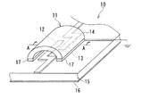
図1に本発明の実施形態を示すマイクロ波集積回路10に用いられるコプレーナ構造で構成されたインタデジタル型キャパシタ11の斜視図を示す。また、図2に図1のA−A線に沿う断面図を示す。
【0014】
図1および図2によれば、インタデジタル型キャパシタ11は、コプレーナ電極12,13と、橋状接地導体14とを誘電体基板15の上面に備える。一方、誘電体基板15の下面には下部接地導体16を備える。誘電体基板15の上面には、コプレーナ電極12,13が互いに対向して設けられる。また、コプレーナ構造で構成されたインタデジタル型キャパシタ11のため、コプレーナ電極12,13が対向する外側には、接地導体17が存在する。コプレーナ電極12,13の上方には、半楕円筒(半筒)状のシート部材で形成された橋状接地導体14がコプレーナ電極12,13を覆う様に跨設され、両接地導体17と電気的に接続される。即ち、橋状接地導体14は接地導体17,17間をブリッジ結合しており、コプレーナ電極12,13に跨設される。
【0015】
インタデジタル型キャパシタ11は、コプレーナ電極12,13の上方に橋状接地導体14を橋を架ける様にして設けることで、橋状接地導体14がシールド板と同じ効果を果たしている。この橋状接地導体14のシールド効果によって、インタデジタル型キャパシタ11は、クロストークの要因となる外部回路の素子と間の結合電荷容量をほとんど持たない。従って、クロストークをはるかに低減出来る。
【0016】
また、マイクロ波集積回路10において、近接する外部回路との間に結合電荷容量を持ち得るのは、キャパシタ成分なので、インタデジタル型キャパシタ11において、外部回路との結合電荷容量を小さく抑えられれば、マイクロ波集積回路10全体としてのクロストーク低減を図ることが出来る。
【0017】
図3に本発明のマイクロ波集積回路10に備えられるインタデジタル型キャパシタ11の電荷容量値を表す等価回路を示す。図5に示される従来のインタデジタル型キャパシタ1の電荷容量値はコプレーナ電極2とコプレーナ電極3との間の結合電荷容量値、つまりCcのみで決定していた。しかし、図3(A)によれば、インタデジタル型キャパシタ11は、コプレーナ電極12,13との間の結合電荷容量値Ccの他に、それぞれのコプレーナ電極12,13と橋状接地導体14との間の電荷容量値Cp(Cp>0)、接地―電極間電荷容量値を持つ。
【0018】
図3(A)の等価回路をより具体化した等価回路が図3(B)である。この図によれば、インタデジタル型キャパシタ11の電荷容量値は、Ccの電荷容量値のキャパシタと、Cpの電荷容量値のキャパシタを2つ直列接続したキャパシタとを並列接続したキャパシタの電荷容量値と等しくなる。従って、インタデジタル型キャパシタ11の電荷容量値は、従来のインタデジタル型キャパシタ1の電荷容量値よりも大きくなる。
【0019】
本発明の実施形態によれば、橋状接地導体14をコプレーナ電極12,13の上方に跨設したインタデジタル型キャパシタ11を備えるマイクロ波集積回路10は、橋状接地導体14がシールドの役目を果たすので、外部回路とのクロストークをはるかに減少させ、マイクロ波集積回路10および外部回路に与える影響を低減出来る。また、インタデジタル型キャパシタ11の電荷容量値は、従来のインタデジタル型キャパシタ1の電荷容量値と比べて大きくなり、回路設計上の自由度が拡がる。
【0020】
尚、本実施形態におけるマイクロ波集積回路10において、橋状接地導体14は半楕円筒状で形成されているが、半楕円筒状に限定されない。あらゆる半筒状を包含する。即ち、橋状接地導体14は半円状で形成されても良いし、半角筒状で形成されても良い。
【0021】
また、この橋状接地導体14をコプレーナ電極12,13の上方に跨設したインタデジタル型キャパシタの数量は少なくとも1つ以上存在すれば良い。
【0022】
さらに、本実施形態におけるマイクロ波集積回路10に備えられるインタデジタル型キャパシタ11は、誘電体基板15の下面に下部接地導体16を備えているが、この下部接地導体16は無くても良い。
【0023】
【発明の効果】
本発明に係るマイクロ波集積回路では、マイクロ波集積回路に使用されるコプレーナ構造で構成されたインタデジタル型キャパシタにおいて、コプレーナ電極上方に橋状接地導体を跨設することで、外部回路とのクロストークを減少させ、マイクロ波集積回路および外部回路に与える影響を低減させ、かつ、インタデジタル型キャパシタの電荷容量値の増加を図ったマイクロ波集積回路を提供することが出来る。
【図面の簡単な説明】
【図1】本発明に係るマイクロ波集積回路に備えられるインタデジタル型キャパシタの斜視図。
【図2】本発明に係るマイクロ波集積回路に備えられるインタデジタル型キャパシタの斜視図におけるA−A線に沿う断面図。
【図3】本発明に係るマイクロ波集積回路に備えられるインタデジタル型キャパシタの電荷容量値を表す等価回路。
【図4】従来のマイクロ波集積回路に備えられるインタデジタル型キャパシタの構成概要図。
【図5】従来のマイクロ波集積回路に備えられるインタデジタル型キャパシタの電荷容量値を表す等価回路。
【符号の説明】
10 マイクロ波集積回路
11 インタデジタル型キャパシタ
12,13 コプレーナ電極
14 橋状接地導体
15 誘電体基板
16 下部接地導体
17 接地導体[0001]
BACKGROUND OF THE INVENTION
The present invention relates to a microwave integrated circuit, and more particularly to a microwave integrated circuit in which an upper portion of a coplanar electrode is covered with a bridge-like ground conductor in an interdigital capacitor having a coplanar structure.
[0002]
[Prior art]
In the microwave integrated circuit, a part of the microwave signal is radiated to the outside due to the transmission characteristics of the microwave. For this reason, the microwave signal radiated to the outside may cause crosstalk with an external circuit adjacent to the microwave integrated circuit. From the viewpoint of this external circuit, the emitted microwave signal is noise. This noise may affect circuit characteristics. On the contrary, noise from an external circuit that is close may affect the circuit characteristics of the microwave integrated circuit. Therefore, measures are taken so that a part of the microwave signal does not crosstalk with the adjacent external circuit. Generally, a shield made of a metal plate such as a copper plate is provided on the entire microwave integrated circuit.
[0003]
FIG. 4 shows an interdigital capacitor 1 having a coplanar structure used in a microwave integrated circuit. An equivalent circuit of the interdigital capacitor 1 is shown in FIG. Note that Cc (Cc> 0) in FIG. 5 indicates a combined charge capacity value.
[0004]
According to FIG. 4, the interdigital capacitor 1 provided in the microwave integrated circuit includes
[0005]
On the other hand, according to FIG. 5, the charge capacity value of the interdigital capacitor 1 is determined only by Cc between the
[0006]
[Problems to be solved by the invention]
However, miniaturization and integration of microwave integrated circuits have progressed, and there are situations in which microwave integrated circuits and external circuits are not necessarily shielded by a shield. In this case, in the interdigital capacitor 1 used in the microwave integrated circuit, the
[0007]
In addition, the conventional interdigital capacitor has a small charge capacity value, and the degree of freedom in circuit design in micro integrated circuit design is narrowed.
[0008]
The present invention has been made in consideration of the above-described circumstances. The present invention reduces crosstalk between a microwave integrated circuit and an external circuit adjacent thereto, and reduces the charge capacity value of an interdigital capacitor provided in the microwave integrated circuit. An object is to provide an increased microwave integrated circuit.
[0009]
[Means for Solving the Problems]
In order to solve the above-described problem, a microwave integrated circuit according to the present invention includes, as described in claim 1, a microwave integrated circuit including an interdigital capacitor having a coplanar structure. A bridge-shaped ground conductor is provided between the ground conductors outside the coplanar electrodes facing each other, and the coplanar electrode is covered with the bridge-shaped ground conductor.
[0010]
In order to solve the above-described problem, according to the microwave integrated circuit of the present invention, as described in
[0011]
In the microwave integrated circuit configured as described above, the crosstalk with the external circuit can be reduced and the charge capacity value of the interdigital capacitor can be increased, which has an influence on the microwave integrated circuit and the external circuit. It can be made smaller.
[0012]
DETAILED DESCRIPTION OF THE INVENTION
Embodiments of a microwave integrated circuit according to the present invention will be described below with reference to the accompanying drawings.
[0013]
FIG. 1 shows a perspective view of an
[0014]
According to FIGS. 1 and 2, the
[0015]
In the
[0016]
Further, in the microwave integrated
[0017]
FIG. 3 shows an equivalent circuit representing the charge capacitance value of the
[0018]
FIG. 3B is an equivalent circuit that more specifically embodies the equivalent circuit of FIG. According to this figure, the charge capacity value of the
[0019]
According to the embodiment of the present invention, the microwave integrated
[0020]
In the microwave integrated
[0021]
The number of interdigital capacitors in which the bridge-shaped
[0022]
Furthermore, although the
[0023]
【The invention's effect】
In the microwave integrated circuit according to the present invention, in an interdigital capacitor having a coplanar structure used in a microwave integrated circuit, a bridge-like ground conductor is straddled above the coplanar electrode, thereby crossing with an external circuit. It is possible to provide a microwave integrated circuit in which the talk is reduced, the influence on the microwave integrated circuit and the external circuit is reduced, and the charge capacity value of the interdigital capacitor is increased.
[Brief description of the drawings]
FIG. 1 is a perspective view of an interdigital capacitor provided in a microwave integrated circuit according to the present invention.
FIG. 2 is a cross-sectional view taken along line AA in the perspective view of the interdigital capacitor provided in the microwave integrated circuit according to the present invention.
FIG. 3 is an equivalent circuit representing a charge capacity value of an interdigital capacitor provided in the microwave integrated circuit according to the present invention.
FIG. 4 is a schematic configuration diagram of an interdigital capacitor provided in a conventional microwave integrated circuit.
FIG. 5 is an equivalent circuit showing a charge capacity value of an interdigital capacitor provided in a conventional microwave integrated circuit.
[Explanation of symbols]
DESCRIPTION OF
Claims (2)
Priority Applications (1)
| Application Number | Priority Date | Filing Date | Title |
|---|---|---|---|
| JP2001397488A JP3934417B2 (en) | 2001-12-27 | 2001-12-27 | Microwave integrated circuit |
Applications Claiming Priority (1)
| Application Number | Priority Date | Filing Date | Title |
|---|---|---|---|
| JP2001397488A JP3934417B2 (en) | 2001-12-27 | 2001-12-27 | Microwave integrated circuit |
Publications (3)
| Publication Number | Publication Date |
|---|---|
| JP2003197758A JP2003197758A (en) | 2003-07-11 |
| JP2003197758A5 JP2003197758A5 (en) | 2005-05-26 |
| JP3934417B2 true JP3934417B2 (en) | 2007-06-20 |
Family
ID=27603265
Family Applications (1)
| Application Number | Title | Priority Date | Filing Date |
|---|---|---|---|
| JP2001397488A Expired - Fee Related JP3934417B2 (en) | 2001-12-27 | 2001-12-27 | Microwave integrated circuit |
Country Status (1)
| Country | Link |
|---|---|
| JP (1) | JP3934417B2 (en) |
Families Citing this family (2)
| Publication number | Priority date | Publication date | Assignee | Title |
|---|---|---|---|---|
| WO2020225856A1 (en) * | 2019-05-07 | 2020-11-12 | 三菱電機株式会社 | Cascode power amplifier |
| CN115458334B (en) * | 2022-08-31 | 2023-10-27 | 电子科技大学 | Columnar interdigital supercapacitor |
-
2001
- 2001-12-27 JP JP2001397488A patent/JP3934417B2/en not_active Expired - Fee Related
Also Published As
| Publication number | Publication date |
|---|---|
| JP2003197758A (en) | 2003-07-11 |
Similar Documents
| Publication | Publication Date | Title |
|---|---|---|
| JP3087495B2 (en) | Capacitors and shield cases | |
| JP6151794B2 (en) | Circuit board, electronic component storage package, and electronic device | |
| JP4241732B2 (en) | Noise filter mounting structure | |
| JPH08279667A (en) | Flexible board | |
| JP3756129B2 (en) | Transmission line type noise filter | |
| JPH09274969A (en) | Connector | |
| JP3934417B2 (en) | Microwave integrated circuit | |
| JP2000223905A (en) | Electronic device | |
| JP2002150848A (en) | Shield flat cable and connection method of the same | |
| JP2010080744A (en) | Printed circuit board and electronic apparatus | |
| JPH02284501A (en) | Surface mounting type strip line resonator | |
| JP4867838B2 (en) | Dielectric resonant component | |
| JP4240385B2 (en) | Surface mount capacitor | |
| JPH10106684A (en) | Connector | |
| JP2005123520A (en) | Printed circuit | |
| JP3135443B2 (en) | Multilayer ceramic capacitors | |
| JPH0326598A (en) | Electronic circuit unit | |
| JPWO2019215922A1 (en) | connector | |
| JPH06295772A (en) | Noise filter block and connector having the block | |
| JP3061092B2 (en) | Noise filter block with varistor function | |
| JP4460855B2 (en) | filter | |
| JP2001326439A (en) | Manufacturing method of printed circuit and portable communication equipment | |
| JP6687302B1 (en) | High frequency circuit and communication module | |
| JP6250229B1 (en) | Printed board | |
| JP2604203Y2 (en) | Ceramic capacitors |
Legal Events
| Date | Code | Title | Description |
|---|---|---|---|
| A521 | Written amendment |
Free format text: JAPANESE INTERMEDIATE CODE: A523 Effective date: 20040726 |
|
| A621 | Written request for application examination |
Free format text: JAPANESE INTERMEDIATE CODE: A621 Effective date: 20040726 |
|
| A977 | Report on retrieval |
Free format text: JAPANESE INTERMEDIATE CODE: A971007 Effective date: 20061120 |
|
| A131 | Notification of reasons for refusal |
Free format text: JAPANESE INTERMEDIATE CODE: A131 Effective date: 20061128 |
|
| TRDD | Decision of grant or rejection written | ||
| A01 | Written decision to grant a patent or to grant a registration (utility model) |
Free format text: JAPANESE INTERMEDIATE CODE: A01 Effective date: 20070306 |
|
| A61 | First payment of annual fees (during grant procedure) |
Free format text: JAPANESE INTERMEDIATE CODE: A61 Effective date: 20070315 |
|
| LAPS | Cancellation because of no payment of annual fees |