JP3922337B2 - Liquid impurity source material and semiconductor device manufacturing method using the same - Google Patents
Liquid impurity source material and semiconductor device manufacturing method using the same Download PDFInfo
- Publication number
- JP3922337B2 JP3922337B2 JP2000257741A JP2000257741A JP3922337B2 JP 3922337 B2 JP3922337 B2 JP 3922337B2 JP 2000257741 A JP2000257741 A JP 2000257741A JP 2000257741 A JP2000257741 A JP 2000257741A JP 3922337 B2 JP3922337 B2 JP 3922337B2
- Authority
- JP
- Japan
- Prior art keywords
- impurity source
- semiconductor substrate
- source material
- liquid impurity
- phosphorus
- Prior art date
- Legal status (The legal status is an assumption and is not a legal conclusion. Google has not performed a legal analysis and makes no representation as to the accuracy of the status listed.)
- Expired - Fee Related
Links
Images

Description
【0001】
【発明の属する技術分野】
本発明は、半導体基体にリンを拡散させるための液状不純物源材料、及びこの液状不純物源材料を使用して半導体基体に拡散領域を形成してトランジスタ、サイリスタ、ダイオ−ド等の半導体装置を製造する方法に関する。
【0002】
【従来の技術】
シリコン半導体基体にn形半導体領域を形成するための不純物源材料としてリンを含む液状不純物源材料が知られている。これを使用してn形不純物拡散領域を形成する時には、アルコ−ルなどの有機溶媒にn形不純物としてのリンを溶解してなる液状不純物を周知のスピンナ方法によってシリコン半導体基体の表面に塗布して液状不純物被膜を形成し、次に、このシリコン半導体基体に120〜140℃程度の熱処理を施し、この液状不純物被膜をベ−キングして有機溶剤を蒸発させて拡散源膜を形成し、続いて、このシリコン半導体基体に窒素雰囲気中で1200℃程度の熱処理を施すことによって拡散源膜中のリンを半導体基体内に拡散する。
【0003】
【発明が解決しようとする課題】
ところで、従来のリンを含む液状不純物源は、アルコ−ルなどの有機溶媒と無機リン化合物との混合物からなっている。ここで、リン化合物として無機リン化合物を使用するのは、無機リン化合物が有機溶媒に対して良好に溶解するためである。
しかし、無機リン化合物は吸湿性が高いため、無機リン化合物と有機溶媒とを混合してなる液状不純物を使用すると、シリコン半導体基体表面に拡散源膜を安定して形成できないという問題点があった。即ち、リン化合物の吸湿により液状不純物源が半導体基体の裏面側まで回り込んだり、液状不純物被膜をベ−キングしてからしばらくの時間放置するとリン化合物の吸湿によってリンを含む水滴が拡散源膜の表面に形成されることがあった。これらの不純物源の回り込みや水滴の発生は、シリコン半導体基体に均質な拡散領域を安定して形成するにあたって問題となる。
ここで無機リン化合物として吸湿性の少ないものを使用することも考えられるが、この種の吸湿性の少ない無機リン化合物は水には比較的良好に溶解するがアルコ−ルなどの有機溶媒には良好に溶解しない為、液状不純物源のリン化合物として使用することはできなかった。
【0004】
そこで、本発明の第1の目的は、リンを含む拡散源膜を良好に形成することのできる液状不純物源材料、及びそれを使用した半導体装置の製造方法を提供することにある。
また、本発明の第2の目的は、リンを含む拡散源膜を良好に形成することができ且つシリコン半導体基体に対する濡れ性が良い液状不純物源材料、及びそれを使用した半導体装置の製造方法を提供することにある。
【0005】
【課題を解決するための手段】
上記第1の目的を達成するための請求項1の発明に従う液状不純物源材料は、アルキル基の炭素数が3又は3よりも大きい亜リン酸エステル又はオルトリン酸エステルから成る有機リン化合物と溶剤とを含むことを特徴とするものである。
なお、請求項2に示すように、液状不純物源に増粘剤を加えること、又は請求項3に示すように界面活性剤を加えることができる。
上記第1の目的を達成するための請求項4の発明に従う半導体装置の製造方法は、半導体基体の表面にアルキル基の炭素数が3又は3よりも大きい亜リン酸エステル又はオルトリン酸エステルから成る有機リン化合物と溶剤とを含む液状不純物源材料を塗布する工程と、塗布された液状不純物源材料に対して室温から200℃の範囲の温度の熱処理を施して溶剤を揮発させてリンを含む不純物源膜を形成する工程と、この不純物源膜に対して1260℃の熱処理を施して前記半導体基体に前記不純物源膜のリンを拡散させる工程とを備えていることを特徴とするものである。
【0006】
上記第2の目的を達成するための請求項5の発明に従う液状不純物源材料は、アルキル基の炭素数が3又は3よりも大きい亜リン酸エステル又はオルトリン酸エステルから成る有機リン化合物と溶剤と珪素又は珪素化合物とを含むことを特徴とするものである。
なお、請求項6に示すように、請求項5の液状不純物源材料に界面活性剤を加えることができる。
上記第2の目的を達成するための請求項7の発明に従う半導体装置の製造方法は、半導体基体の表面にアルキル基の炭素数が3又は3よりも大きい亜リン酸エステル又はオルトリン酸エステルから成る有機リン化合物と溶剤と珪素又は珪素化合物とを含む液状不純物源材料を塗布する工程と、塗布された液状不純物源材料に対して室温から200℃の範囲の温度の熱処理を施して溶剤を揮発させてリンを含む不純物源膜を形成する工程と、この不純物源膜に対して1260℃の熱処理を施して前記半導体基体に前記不純物膜のリンを拡散させる工程とを備えていることを特徴とするものである。
【0007】
各請求項の発明における有機リン化合物としての亜リン酸エステルは、吸湿性が少なく且つ有機溶剤に可溶な、
アルキルホスホン酸ジエステル [CnH2n+1PO3(CxH2x+1)2]又は
アルキルホスホン酸モノエステル [CnH2n+1PO3HCxH2x+1]
であることが望ましい。なお、上記各エステルにおいてn及びxは3又は3よりも大きい値であることが望ましい。
また、オルトリン酸エステルは、吸湿性が少なく且つ有機溶剤に可溶な、
トリフェニルホスフェ−ト [(C6H5O)3PO]又は
レゾルシノ−ルビスジフェニルホスフェ−ト[(C12H9O)2HOC6H4OPO]
であることが望ましい。
【0008】
請求項1〜4の発明における溶剤は、有機リン化合物を溶解することが可能なものから選択される。
請求項2の発明に従って、増粘剤を添加する場合における溶剤は有機リン化合物と増粘剤との両方を溶解させることができるものから選択される。
また、請求項5〜7の発明に従って珪素又は珪素化合物を添加する場合における溶剤は、有機リン化合物と珪素又は珪素化合物との両方を溶解させることができるものから選択される。
請求項1〜7の発明の溶剤として、例えば、アルコ−ル系溶剤、エチレングリコ−ル誘導体を使用することができる。アルコ−ル系溶剤として、
メタノ−ル [CH3OH]、
エタノ−ル [CH3CH2OH]、
1−フロパノ−ル [CH3CH2CH2OH]、
2−プロパノ−ル [CH3CH(OH)CH3]
が適している。
エチレングリコ−ル誘導体として、
2−メトキシエタノ−ル [CH3OCH2CH2OH]
2−エトキシエタノ−ル [CH3CH2OCH2CH2OH]
2−メトキシエチルアセテ−ト [CH3OCH2CH2OOCCH3]
2−(2−メトキシエトキシ)エタノ−ル [CH3OCH2CH2OCH2CH2OH]
1,2−ジメトキシエタン [CH3OCH2CH2OCH3]
1,2−ジエトキシエタン [CH3CH2OCH2CH2OCH2CH3]
が適している。
【0009】
請求項2の発明の増粘剤としては、拡散工程又はこの前の熱処理によって燃焼して残渣として残らず且つ溶剤に対して可溶であり且つ有機リン化合物との相溶性が良好なものが使用され、例えば、ポリビニルブチラ−ル、ヒドロキシプロピルセルロ−ス、エチルセルロ−ス、酢酸セルロ−ス、市販のアクリル系レジン、ポリビニルメチルエ−テル等の樹脂が使用可能である。
【0010】
請求項3及び7の界面活性剤としては、半導体基体に対する液状不純物源材料の濡れ性を改善することができるもの又は気泡の発生を抑えることができるもの又はこれ等の両方の働きを有するものが使用され、例えば、フッ素系界面活性剤を使用することができる。
【0011】
請求項5〜7の発明に従う珪素化合物としては、RnSi(OH)4-n(但し、Rはアルキル基nは任意の数値)で示すことができるシラノ−ル系化合物が適し、揮発性が余り高くなく、且つ危険性の少ないものを使用する。
【0012】
【発明の効果】
請求項1〜4の発明によれば、アルキル基の炭素数が3又は3よりも大きい亜リン酸エステル又はオルトリン酸エステルから成る有機リン化合物は無機リン化合物に比較して吸湿性が少ないために安定且つ均一の不純物源膜を形成することができ、均質な不純物拡散領域を安定的に得ることができる。即ち、アルキル基の炭素数が3又は3よりも大きい亜リン酸エステル又はオルトリン酸エステルから成る有機リン化合物からなる不純物源膜は吸湿性が少なく、また空気中に放置しても水滴が形成され難いため、均質な拡散領域を安定して形成することができる。また、アルキル基の炭素数が3又は3よりも大きい亜リン酸エステル又はオルトリン酸エステルから成る有機リン化合物はアルコ−ルなどの溶剤に良好に溶解するので、液状不純物源として十分に実用に供することができる。
また、請求項2の発明によれば増粘剤によって液状不純物原材料の粘度を適当な値にすることができ、不純物源膜を良好に形成することができる。
また、請求項3の発明によれば、半導体基体に対する液状不純物原の濡れ性を向上させることができる。
また、請求項4の発明によれば、不純物源膜を形成する工程を拡散工程の前に設けたので、不純物源膜から拡散を安定的に進めることができる。また、不純物源膜におけるリンの量によって拡散の深さ及び不純物濃度を制御することができる。
また、請求項5〜7の発明は、請求項1〜4の発明と同様な効果を有する他に、
次の効果を有する。即ち、珪素又は珪素化合物の働きによって液状不純物源の半導体基体に対する濡れ性が向上し、半導体基体の表面にむらの少ない均一な厚みの不純物源膜を形成することができ、均質な不純物拡散領域を安定的に得ることができる。
また、請求項6の発明は、請求項3の発明と同様な効果を得ることができる。
また、請求項7の発明は、請求項4の発明と同様な効果を得ることができる。
【0013】
【実施形態及び実施例】
次に、図1及び図2を参照して本発明の実施形態及び実施例を説明する。
【0014】
【第1の実施例】
まず、半導体基体としてP形のシリコン半導体基板1即ちウェハを用意した。また、次に示す組成の液状不純物源材料を用意した。
有機リン化合物としてのアルキルホスホン酸ジエステル(分子量約350):7重量%
溶剤としての2−メトキシエタノ−ル:84.5重量%
増粘剤としてのヒドロキシプロピルセルロ−ス:8.5重量%
フッ素系界面活性剤:10ppm
【0015】
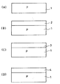
次に、この液状不純物源材料を、周知のスピンナ方法によって半導体基板1の一方の主面即ち不純物拡散予定領域の表面に均一に塗布して液状不純物源層2を図1(B)に概念的に示すように形成する。本実施例では、液状不純物源のスピンナ塗布形成時における半導体基板の回転数を3000〜4000rpmに設定した。本実施例では、吸湿性が小さい有機リン化合物を使用しているので、スピンナで形成した液状不純物源層2の保存安定性が良く、時間が経過しても半導体ウェハの裏面までに液状不純物源材料が回り込まない。
【0016】
次に、図1(B)に示す不純物源層2を形成した半導体基板1をホットプレ−ト(ヒ−トプレ−ト)上に配置し、この不純物源層2を伴った半導体基板1に対してリンの拡散温度よりも低い室温から200℃の範囲の温度、好ましくは150〜200℃で熱処理を施して、液状不純物源層2に含まれる溶剤を揮発させ、図1(C)に示すように半導体基板1の一方の主面に有機リン化合物を含む不純物源膜3を形成する。この溶剤揮発処理は空気中で行う。この溶剤揮発処理後の不純物源膜3は、吸湿性が少ないものから成るので、空気中に放置しても不純物源膜3に水滴が形成されない。
【0017】
次に、図1(C)に示す不純物源膜3を有する半導体基板1を石英やSiC(シリコンカ−バイト)から構成される半導体基板拡散用ホルダ−にチャ−ジした後に、これを石英やSiC等から構成されるプロセスチュ−ブ内に入れて所定の温度プロフアイルの熱処理を施す。即ち、チュ−ブ内に酸素を導入してチュ−ブ内を酸化雰囲気とした状態で拡散温度(1260℃)よりも低い500〜1000℃の温度まで半導体基板を徐々に加熱し、この状態を30〜100分間保つ。酸素雰囲気で不純物源膜3を加熱することにより、リンの酸化物が生成され、且つ増粘剤は焼消し、図1に示すリン酸化合物から成る不純物源膜4が形成される。
【0018】
次に、温度を500〜1000℃に保って雰囲気を窒素(N2)雰囲気(非酸化性雰囲気)に置き換えて約30分間加熱処理した後に、加熱温度を1260℃に上げ、窒素雰囲気中で所定時間(例えば5時間)の熱処理を施して不純物源膜4からリンを半導体基板1に拡散させ、図2(E)に示すN形半導体領域5を得る。なお、半導体基板1にはP形半導体領域1aが残存し、PN接合が形成される。
【0019】
次に、図2(E)の半導体基板1に弗酸又はこれを主成分とする弗酸系エッチング液でエッチングを施して、半導体基板1の一方の主面に残存した不純物源膜4を除去して、図2(F)に示すように半導体基板1の一方の主面にN形半導体領域5を露出させる。本実施形態では、上述のようにシリコン半導体基板1の一方の主面が窒化されることがないため、半導体基板1の一方の主面に形成された不純物源膜4から成る残さ被膜を容易に且つ完全に除去することができる。
【0020】
次に、図2(G)に示すようにN形半導体領域5の上に金属オ−ミック電極6を形成する。なお、図2(G)では省略されているが、P形半導体領域1aに必要に応じてN形半導体領域等を形成し、周知のトランジスタ、サイリスタ等を構成する。
【0021】
本実施例によれば次の効果を得ることができる。
(1) 無機リン化合物に比べて吸湿性の低い有機リン化合物を含む液状不純物源材料を使用するので、スピンナ−で液状不純物源層2を形成した時に、ウェハ即ち半導体基板1の裏面側に液状不純物減材料が回り込むことを防ぐことができる。換言すれば、半導体基板1に対する濡れ性を比較的良好に保っても、液状不純物源材料のウェハ裏面への回り込みを防ぐことができる。
(2) 吸湿性の低い有機リン化合物を使用しているので、液状不純物源を150〜200℃で熱処理した後の不純物源膜3も吸湿性が低く、空気中に放置しても水滴が形成されず、安定性の高い不純物源膜を提供することができる。
(3) 液状不純物源材料におけるリンの濃度の調整が容易であり、結果として半導体基板1におけるリン拡散領域の不純物濃度及び深さの制御が容易になる。
(4) 有機リン化合物は吸湿性が低いので、不純物源膜におけるリンの濃度を高めることができ、1020cm-3以上の高い不純物濃度の拡散領域の形成、及び50μm程度の深い拡散領域の形が可能になる。
(5) 拡散後に半導体基板1の表面に残存したものを弗酸にて容易に除去することができる。
(6) 液状不純物源材料を密閉容器に充填し、光の当たらない場所で室温に保つと、長期の保存が可能である。
(7) 増粘剤によって液状不純物源材料の粘度を適当な値にすることができ、任意の不純物濃度の拡散領域を容易に形成することができる。
(8)界面活性剤によって濡れ性を向上させることができる。
【0022】
【第2の実施例】
第2の実施例においては、液状不純物源材料としての次の組成物を用意した。
有機リン化合物として トリフェニルホスフェ−ト:10重量%
溶剤として 2−エトキシエタノ−ル:80重量%
増粘剤として ヒドロキシプロピルセルロ−ス:10重量%
界面活性剤として フッ素界面活性剤:10ppm
液状不純物源材料を上記の組成とした他は、第1の実施例と同一の方法でN形拡散領域を形成した。
この第2の実施例によっても第1の実施例と同一の効果を得ることができる。
【0023】
【第3の実施例】
第3の実施例では、液状不純物源材料として次の組成物を用意した。
有機リン化合物として アルキルホスホン酸ジエステル(分子量約350):7重量%
溶剤として 2−メトキシエタノ−ル:84.5重量%
濡れ性向上用又はガラス化用として 珪素化合物:8.5重量%
液状不純物源材料を上記組成に変えた他は、第1の実施例と同一の方法でN形不純物拡散領域を形成した。
【0024】
この第3の実施例によれば、有機リン化合物を使用するので、第1の実施例で述べた効果(1)、(2)、(3)、(4)、(5)、(6)と同一の効果を得ることができ、更に、珪素化合物の添加によって濡れ性が向上するという効果も得ることができる。更に、本実施例によれば、拡散前の500〜1000℃の熱処理によって不純物源膜の珪素化合物即ちシラノ−ルの酸化及びリンの酸化が生じ、リンの酸化物P2O5が添加されたSiO2膜から成るPSG膜(phospho silicate glass)が生じるので、窒素の雰囲気中の拡散工程において半導体基板の表面に窒化膜が形成されることをs防ぐことができ、半導体基板表面の残さの除去が容易になる。
なお、PSG膜が不純物源膜となって半導体基板にリンが拡散する。
【0025】
【第4の実施例】
第4の実施例では、液状不純物源材料として、次の組成物を用意した。
有機リン化合物として トリフェニルホスフェ−ト:10重量%
溶剤として 2−エトキシエタノ−ル:80重量%
濡れ性向上又はガラス化用としての 珪素化合物:10重量%
界面活性剤としての フッ素界面活性剤:10ppm
液状不純物源材料を上記組成とした他は第1の実施例と同一の方法でN形拡散領域を形成した。
【0026】
第4の実施例によれば、第3の実施例と同一の効果を得ることができ、更に界面活性剤によって濡れ性が向上するという効果が得られる。
【0027】
【変形例】
本発明は上記実施例に限定されるものでなく、例えば次の変形が可能なものである。
(1) 第1及び第2の実施例の液状不純物源材料から増粘剤を除去した物から成る液状不純物源材料を使用しても第1及び第2の実施例と同じ方法でN型拡散領域をそれぞれ形成したところ、増粘剤の効果以外の効果を第1及び第2の実施例と同様に得ることができた。
(2) 第1、第2、第3及び第4の実施例の液状不純物源材料から界面活性剤を除去したものから成る液状不純物源材料を使用しても第1、第2、第3及び第4の実施例と同じ方法でN形拡散領域をそれぞれ形成したところ、界面活性剤の効果以外の効果を第1、第2、第3及び第4の実施例と同様に得ることができた。
(3) 第1及び第2実施例の液状不純物源材料から増粘剤と界面活性剤とを除去したものから成る液状不純物源材料を使用しても第1及び第2の実施例と同じ方法でN形拡散領域をそれぞれ形成したところ、増粘剤と界面活性剤の効果以外の効果を第1及び第2の実施例と同様に得ることができた。
(4) 第3及び第4の実施例の液状不純物源材料に第1及び第2実施例と同様に増粘剤を添加することができる。
(5) 窒素雰囲気の代わりにアルゴン等の非酸化性雰囲気で不純物を拡散する場合においても、弗酸又はこれを主成分とするエッチング液で除去し難いシリコン化合物が形成されることがある。従って、本発明は、この場合にも適用可能である。
(6) 液状不純物源を半導体基板1の特定領域即ち拡散予定領域のみに塗布することができる。
(7) オ−ミック電極9の代わりにショットキバリア電極、FETのゲ−ト絶縁膜等をN形半導体領域5の表面に形成することができる。
【図面の簡単な説明】
【図1】本発明に実施例に従う半導体装置の製造方法を工程順に説明するための概略断面図である。
【図2】図1の工程の続きの工程を説明するための断面図である。
【符号の説明】
1 半導体基板
2 液状不純物源層
5 N形半導体領域[0001]
BACKGROUND OF THE INVENTION
The present invention manufactures a semiconductor device such as a transistor, a thyristor, or a diode by forming a liquid impurity source material for diffusing phosphorus in a semiconductor substrate and forming a diffusion region in the semiconductor substrate using the liquid impurity source material. On how to do.
[0002]
[Prior art]
A liquid impurity source material containing phosphorus is known as an impurity source material for forming an n-type semiconductor region in a silicon semiconductor substrate. When an n-type impurity diffusion region is formed using this, a liquid impurity obtained by dissolving phosphorus as an n-type impurity in an organic solvent such as alcohol is applied to the surface of the silicon semiconductor substrate by a known spinner method. Then, a liquid impurity film is formed, and then the silicon semiconductor substrate is subjected to a heat treatment at about 120 to 140 ° C., and the liquid impurity film is baked to evaporate the organic solvent to form a diffusion source film. Then, the silicon semiconductor substrate is subjected to heat treatment at about 1200 ° C. in a nitrogen atmosphere to diffuse phosphorus in the diffusion source film into the semiconductor substrate.
[0003]
[Problems to be solved by the invention]
By the way, the conventional liquid impurity source containing phosphorus consists of a mixture of an organic solvent such as alcohol and an inorganic phosphorus compound. Here, the inorganic phosphorus compound is used as the phosphorus compound because the inorganic phosphorus compound dissolves well in the organic solvent.
However, since the inorganic phosphorus compound has high hygroscopicity, there is a problem that a diffusion source film cannot be stably formed on the surface of the silicon semiconductor substrate when a liquid impurity formed by mixing an inorganic phosphorus compound and an organic solvent is used. . That is, the liquid impurity source wraps around to the back side of the semiconductor substrate due to moisture absorption of the phosphorus compound, or if the liquid impurity film is baked for a while after being baked, water droplets containing phosphorus are formed on the diffusion source film by moisture absorption of the phosphorus compound. Sometimes formed on the surface. The wraparound of these impurity sources and the generation of water droplets become a problem in stably forming a homogeneous diffusion region in the silicon semiconductor substrate.
Here, it is conceivable to use an inorganic phosphorus compound having a low hygroscopic property, but this kind of an inorganic phosphorus compound having a low hygroscopic property dissolves relatively well in water, but an organic solvent such as an alcohol does not. Since it did not dissolve well, it could not be used as a phosphorus compound as a liquid impurity source.
[0004]
Accordingly, a first object of the present invention is to provide a liquid impurity source material capable of satisfactorily forming a diffusion source film containing phosphorus, and a method of manufacturing a semiconductor device using the same.
A second object of the present invention is to provide a liquid impurity source material that can satisfactorily form a diffusion source film containing phosphorus and has good wettability with respect to a silicon semiconductor substrate, and a method of manufacturing a semiconductor device using the same. It is to provide.
[0005]
[Means for Solving the Problems]
In order to achieve the first object, the liquid impurity source material according to the invention of
In addition, as shown in
In order to achieve the first object, a method of manufacturing a semiconductor device according to the invention of claim 4 comprises a phosphite or orthophosphate having 3 or more than 3 carbon atoms in the alkyl group on the surface of the semiconductor substrate. A step of applying a liquid impurity source material containing an organophosphorus compound and a solvent; and an impurity containing phosphorus by volatilizing the solvent by subjecting the applied liquid impurity source material to a heat treatment at a temperature in the range of room temperature to 200 ° C. The method includes a step of forming a source film, and a step of performing a heat treatment at 1260 ° C. on the impurity source film to diffuse phosphorus of the impurity source film into the semiconductor substrate.
[0006]
In order to achieve the second object, the liquid impurity source material according to the invention of
As shown in
A method of manufacturing a semiconductor device according to the invention of claim 7 for achieving the second object comprises a phosphite ester or an orthophosphate ester having 3 or more than 3 carbon atoms in the alkyl group on the surface of the semiconductor substrate. A step of applying a liquid impurity source material containing an organophosphorus compound, a solvent, and silicon or a silicon compound, and subjecting the applied liquid impurity source material to a heat treatment at a temperature ranging from room temperature to 200 ° C. to volatilize the solvent. Forming an impurity source film containing phosphorus, and subjecting the impurity source film to a heat treatment at 1260 ° C. to diffuse phosphorus in the impurity film into the semiconductor substrate. Is.
[0007]
Phosphites and organic phosphorus compounds in the invention of each claim, soluble in small and organic solvent hygroscopicity,
Alkylphosphonic acid diester [C n H 2n + 1 PO 3 (C x H 2x + 1 ) 2 ] or alkylphosphonic acid monoester [C n H 2n + 1 PO 3 HC x H 2x + 1 ]
It is desirable that In each of the above esters, n and x are desirably 3 or a value larger than 3.
In addition, orthophosphate is less hygroscopic and soluble in organic solvents ,
Triphenyl phosphate [(C 6 H 5 O) 3 PO] or resorcinol bisdiphenyl phosphate [(C 12 H 9 O) 2 HOC 6 H 4 OPO]
It is desirable that
[0008]
The solvent in the inventions of
According to the invention of
Moreover, the solvent in the case of adding silicon or a silicon compound according to the inventions of
As the solvent of the inventions of
Methanol [CH 3 OH],
Ethanol [CH 3 CH 2 OH],
1-Flopanol [CH 3 CH 2 CH 2 OH],
2-propanol [CH 3 CH (OH) CH 3 ]
Is suitable.
As ethylene glycol derivatives,
2-Methoxyethanol [CH 3 OCH 2 CH 2 OH]
2-Ethoxyethanol [CH 3 CH 2 OCH 2 CH 2 OH]
2-methoxyethyl acetate [CH 3 OCH 2 CH 2 OOCCH 3 ]
2- (2-methoxyethoxy) ethanol [CH 3 OCH 2 CH 2 OCH 2 CH 2 OH]
1,2-dimethoxyethane [CH 3 OCH 2 CH 2 OCH 3 ]
1,2-diethoxyethane [CH 3 CH 2 OCH 2 CH 2 OCH 2 CH 3 ]
Is suitable.
[0009]
As the thickener of the invention of
[0010]
The surfactants according to
[0011]
As the silicon compound according to the inventions of
[0012]
【The invention's effect】
According to the inventions of
According to the invention of
According to the invention of
According to the invention of claim 4, since the step of forming the impurity source film is provided before the diffusion step, diffusion can be stably advanced from the impurity source film. Further, the diffusion depth and impurity concentration can be controlled by the amount of phosphorus in the impurity source film.
The inventions of
It has the following effects. That is, the wettability of the liquid impurity source to the semiconductor substrate is improved by the action of silicon or a silicon compound, and an impurity source film having a uniform thickness with little unevenness can be formed on the surface of the semiconductor substrate. It can be obtained stably.
Further, the invention of
Further, the invention of claim 7 can obtain the same effect as that of the invention of claim 4.
[0013]
Embodiment and Examples
Next, embodiments and examples of the present invention will be described with reference to FIGS.
[0014]
[First embodiment]
First, a P-type
Alkylphosphonic acid diester as an organophosphorus compound (molecular weight about 350): 7% by weight
2-methoxyethanol as solvent: 84.5% by weight
Hydroxypropyl cellulose as thickener: 8.5% by weight
Fluorosurfactant: 10ppm
[0015]
Next, this liquid impurity source material is uniformly applied to one main surface of the
[0016]
Next, the
[0017]
Next, after the
[0018]
Next, after maintaining the temperature at 500 to 1000 ° C. and replacing the atmosphere with a nitrogen (N 2) atmosphere (non-oxidizing atmosphere) for about 30 minutes, the heating temperature is increased to 1260 ° C. and the temperature is kept in the nitrogen atmosphere for a predetermined time. A heat treatment (for example, 5 hours) is performed to diffuse phosphorus from the impurity source film 4 into the
[0019]
Next, the
[0020]
Next, a
[0021]
According to the present embodiment, the following effects can be obtained.
(1) Since a liquid impurity source material containing an organic phosphorus compound that is less hygroscopic than an inorganic phosphorus compound is used, when the liquid
(2) Since an organic phosphorus compound with low hygroscopicity is used, the
(3) It is easy to adjust the concentration of phosphorus in the liquid impurity source material, and as a result, the impurity concentration and depth of the phosphorus diffusion region in the
(4) Since the organophosphorus compound has low hygroscopicity, the concentration of phosphorus in the impurity source film can be increased, formation of a diffusion region having a high impurity concentration of 10 20 cm −3 or more, and a deep diffusion region of about 50 μm Shape becomes possible.
(5) What remains on the surface of the
(6) When the liquid impurity source material is filled in a sealed container and kept at room temperature in a place not exposed to light, long-term storage is possible.
(7) The viscosity of the liquid impurity source material can be adjusted to an appropriate value by the thickener, and a diffusion region having an arbitrary impurity concentration can be easily formed.
(8) The wettability can be improved by the surfactant.
[0022]
[Second embodiment]
In the second example, the following composition as a liquid impurity source material was prepared.
Triphenyl phosphate as organic phosphorus compound: 10% by weight
2-Ethoxyethanol as solvent: 80% by weight
Hydroxypropyl cellulose as a thickener: 10% by weight
As a surfactant Fluorine surfactant: 10ppm
An N-type diffusion region was formed by the same method as in the first example except that the liquid impurity source material had the above composition.
The same effect as that of the first embodiment can be obtained also by the second embodiment.
[0023]
[Third embodiment]
In the third example, the following composition was prepared as a liquid impurity source material.
As an organophosphorus compound, alkylphosphonic acid diester (molecular weight about 350): 7% by weight
2-Methoxyethanol as solvent: 84.5% by weight
For improving wettability or vitrification Silicon compound: 8.5% by weight
An N-type impurity diffusion region was formed by the same method as in the first embodiment except that the liquid impurity source material was changed to the above composition.
[0024]
According to the third embodiment, since an organic phosphorus compound is used, the effects (1), (2), (3), (4), (5), (6) described in the first embodiment are used. In addition, an effect that wettability is improved by adding a silicon compound can be obtained. Furthermore, according to this example, the silicon compound of the impurity source film, that is, silanol, and phosphorus were oxidized by the heat treatment at 500 to 1000 ° C. before diffusion, and phosphorus oxide P 2 O 5 was added. Since a PSG film (phospho silicate glass) composed of a SiO 2 film is generated, it is possible to prevent a nitride film from being formed on the surface of the semiconductor substrate in the diffusion process in a nitrogen atmosphere, and to remove the residue on the surface of the semiconductor substrate. Becomes easier.
Note that the PSG film serves as an impurity source film, and phosphorus diffuses into the semiconductor substrate.
[0025]
[Fourth embodiment]
In the fourth example, the following composition was prepared as a liquid impurity source material.
Triphenyl phosphate as organic phosphorus compound: 10% by weight
2-Ethoxyethanol as solvent: 80% by weight
Silicon compound for wettability improvement or vitrification: 10% by weight
Fluorine surfactant as surfactant: 10ppm
An N-type diffusion region was formed by the same method as in the first embodiment except that the liquid impurity source material had the above composition.
[0026]
According to the fourth embodiment, the same effect as that of the third embodiment can be obtained, and further, the effect of improving the wettability by the surfactant can be obtained.
[0027]
[Modification]
The present invention is not limited to the above embodiment, and for example, the following modifications are possible.
(1) Even if a liquid impurity source material made by removing the thickener from the liquid impurity source material of the first and second embodiments is used, N-type diffusion is performed in the same manner as in the first and second embodiments. When each region was formed, effects other than the effect of the thickener could be obtained in the same manner as in the first and second examples.
(2) The first, second, third and fourth liquid impurity source materials obtained by removing the surfactant from the liquid impurity source materials of the first, second, third and fourth embodiments are also used. When N-type diffusion regions were formed by the same method as in the fourth example, effects other than the effect of the surfactant could be obtained in the same manner as in the first, second, third and fourth examples. .
(3) The same method as in the first and second embodiments, even when a liquid impurity source material made by removing the thickener and the surfactant from the liquid impurity source material in the first and second embodiments is used. When N-type diffusion regions were respectively formed, effects other than those of the thickener and the surfactant could be obtained in the same manner as in the first and second examples.
(4) A thickener can be added to the liquid impurity source materials of the third and fourth embodiments as in the first and second embodiments.
(5) Even when impurities are diffused in a non-oxidizing atmosphere such as argon instead of a nitrogen atmosphere, a silicon compound that is difficult to remove with hydrofluoric acid or an etchant containing the same may be formed. Therefore, the present invention is applicable also in this case.
(6) The liquid impurity source can be applied only to a specific region of the
(7) Instead of the ohmic electrode 9, a Schottky barrier electrode, a gate insulating film of an FET, or the like can be formed on the surface of the N-
[Brief description of the drawings]
FIG. 1 is a schematic cross-sectional view for explaining a method of manufacturing a semiconductor device according to an embodiment of the present invention in the order of steps.
FIG. 2 is a cross-sectional view for explaining a step subsequent to the step of FIG.
[Explanation of symbols]
Claims (7)
半導体基体の表面にアルキル基の炭素数が3又は3よりも大きい亜リン酸エステル又はオルトリン酸エステルから成る有機リン化合物と溶剤とを含む液状不純物源材料を塗布する工程と、
塗布された液状不純物源材料に対して室温から200℃の範囲の温度の熱処理を施して溶剤を揮発させてリンを含む不純物源膜を形成する工程と、
この不純物源膜に対して1260℃の熱処理を施して前記半導体基体に前記不純物源膜のリンを拡散させる工程と
を備えていることを特徴とする半導体装置の製造方法。A method of diffusing phosphorus as an impurity for determining a conductivity type in a semiconductor substrate,
Applying a liquid impurity source material containing an organic phosphorus compound composed of a phosphite or orthophosphate having an alkyl group having 3 or more carbon atoms to the surface of a semiconductor substrate and a solvent;
Applying a heat treatment at a temperature ranging from room temperature to 200 ° C. to the applied liquid impurity source material to volatilize the solvent to form an impurity source film containing phosphorus;
And a step of subjecting the impurity source film to a heat treatment at 1260 ° C. to diffuse phosphorus of the impurity source film into the semiconductor substrate.
半導体基体の表面にアルキル基の炭素数が3又は3よりも大きい亜リン酸エステル又はオルトリン酸エステルから成る有機リン化合物と溶剤と珪素又は珪素化合物とを含む液状不純物源材料を塗布する工程と、
塗布された液状不純物源材料に対して室温から200℃の範囲の温度の熱処理を施して溶剤を揮発させてリンを含む不純物源膜を形成する工程と、
この不純物源膜に対して1260℃の熱処理を施して前記半導体基体に前記不純物膜のリンを拡散させる工程と
を備えていることを特徴とする半導体装置の製造方法。A method of diffusing phosphorus as an impurity for determining a conductivity type in a semiconductor substrate,
Applying a liquid impurity source material comprising an organic phosphorus compound comprising a phosphite or orthophosphate having a carbon number of 3 or greater than 3 on the surface of a semiconductor substrate, a solvent, and silicon or a silicon compound;
Applying a heat treatment at a temperature ranging from room temperature to 200 ° C. to the applied liquid impurity source material to volatilize the solvent to form an impurity source film containing phosphorus;
And a step of subjecting the impurity source film to a heat treatment at 1260 ° C. to diffuse phosphorus of the impurity film into the semiconductor substrate.
Priority Applications (1)
| Application Number | Priority Date | Filing Date | Title |
|---|---|---|---|
| JP2000257741A JP3922337B2 (en) | 2000-08-28 | 2000-08-28 | Liquid impurity source material and semiconductor device manufacturing method using the same |
Applications Claiming Priority (1)
| Application Number | Priority Date | Filing Date | Title |
|---|---|---|---|
| JP2000257741A JP3922337B2 (en) | 2000-08-28 | 2000-08-28 | Liquid impurity source material and semiconductor device manufacturing method using the same |
Publications (2)
| Publication Number | Publication Date |
|---|---|
| JP2002075892A JP2002075892A (en) | 2002-03-15 |
| JP3922337B2 true JP3922337B2 (en) | 2007-05-30 |
Family
ID=18746161
Family Applications (1)
| Application Number | Title | Priority Date | Filing Date |
|---|---|---|---|
| JP2000257741A Expired - Fee Related JP3922337B2 (en) | 2000-08-28 | 2000-08-28 | Liquid impurity source material and semiconductor device manufacturing method using the same |
Country Status (1)
| Country | Link |
|---|---|
| JP (1) | JP3922337B2 (en) |
Families Citing this family (5)
| Publication number | Priority date | Publication date | Assignee | Title |
|---|---|---|---|---|
| DE102005025933B3 (en) * | 2005-06-06 | 2006-07-13 | Centrotherm Photovoltaics Gmbh + Co. Kg | Doping mixture for preparing and doping semiconductor surfaces, comprises a p- or n-dopant, for doping the semiconductor surfaces, water and mixture of two or more surfactants, where one of the surfactant is a non-ionic surfactant |
| KR101631711B1 (en) * | 2008-03-21 | 2016-06-17 | 신에쓰 가가꾸 고교 가부시끼가이샤 | Phosphorus paste for diffusion and method for preparing solar cell by using the same |
| JP2013026524A (en) * | 2011-07-22 | 2013-02-04 | Hitachi Chem Co Ltd | N-type diffusion layer forming composition, manufacturing method of n-type diffusion layer, manufacturing method of solar cell element, and solar cell |
| CN104517820A (en) * | 2013-09-30 | 2015-04-15 | 东京应化工业株式会社 | Diffusant composition, method for forming impurity diffusion layer |
| CN113257953A (en) * | 2021-04-18 | 2021-08-13 | 安徽华晟新能源科技有限公司 | Gettering method and phosphorus gettering device for N-type silicon wafer |
Family Cites Families (7)
| Publication number | Priority date | Publication date | Assignee | Title |
|---|---|---|---|---|
| JPS5279666A (en) * | 1975-12-25 | 1977-07-04 | Matsushita Electronics Corp | Production of transistor |
| JPH0758697B2 (en) * | 1990-06-15 | 1995-06-21 | 信越半導体株式会社 | Method for diffusing impurities in semiconductor device |
| JPH04291729A (en) * | 1991-03-20 | 1992-10-15 | Nec Corp | Manufacture of semiconductor device |
| JPH08283100A (en) * | 1995-04-07 | 1996-10-29 | Mitsubishi Materials Corp | Composition for diffusing phosphorus |
| JP3519847B2 (en) * | 1995-12-26 | 2004-04-19 | 東京応化工業株式会社 | Boron diffusion coating solution |
| JP3522940B2 (en) * | 1995-12-26 | 2004-04-26 | 東京応化工業株式会社 | Boron diffusion coating solution |
| DE19910816A1 (en) * | 1999-03-11 | 2000-10-05 | Merck Patent Gmbh | Doping pastes for producing p, p + and n, n + regions in semiconductors |
-
2000
- 2000-08-28 JP JP2000257741A patent/JP3922337B2/en not_active Expired - Fee Related
Also Published As
| Publication number | Publication date |
|---|---|
| JP2002075892A (en) | 2002-03-15 |
Similar Documents
| Publication | Publication Date | Title |
|---|---|---|
| US6852603B2 (en) | Fabrication of abrupt ultra-shallow junctions | |
| EP2545583B1 (en) | Methods and compositions for doping silicon substrates with molecular monolayers | |
| JPH0376575B2 (en) | ||
| JP3199452B2 (en) | Method of manufacturing P buried layer for PNP device | |
| JP3922337B2 (en) | Liquid impurity source material and semiconductor device manufacturing method using the same | |
| JP2002075894A (en) | Liquid impurity source material, and semiconductor device | |
| US3798081A (en) | Method for diffusing as into silicon from a solid phase | |
| KR20130108271A (en) | Method for producing a sollar cell comprising a selective emitter | |
| JP2005123431A (en) | Liquid impurity source material and method for manufacturing semiconductor device by using same | |
| ES344523A1 (en) | Method of fabricating semiconductor devices | |
| CN114342101A (en) | Impurity diffusion composition, method for manufacturing semiconductor element using same, and method for manufacturing solar cell | |
| JPS5917243A (en) | Manufacture of semiconductor device | |
| JP7463725B2 (en) | P-type impurity diffusion composition and its manufacturing method, manufacturing method of semiconductor element using the same, and solar cell | |
| JP2002075893A (en) | Liquid impurity source material, and semiconductor device | |
| KR20020093875A (en) | Method of doping silicon with phosphorus and growing oxide on silicon in the presence of steam | |
| JP3922334B2 (en) | Manufacturing method of semiconductor device | |
| JP3520911B2 (en) | Method for manufacturing semiconductor device | |
| JPS59182537A (en) | Manufacture of semiconductor device | |
| JPH08283100A (en) | Composition for diffusing phosphorus | |
| JP6838399B2 (en) | Manufacturing method of semiconductor element and manufacturing method of solar cell | |
| JP3039646B1 (en) | Method for manufacturing semiconductor device | |
| JPH0834193B2 (en) | Method for manufacturing semiconductor device | |
| JP3053018B1 (en) | Method for manufacturing semiconductor device | |
| JP2003218048A (en) | Liquid form impurity source material and method of forming diffusion region using the material | |
| JP2810947B2 (en) | Method for manufacturing semiconductor device |
Legal Events
| Date | Code | Title | Description |
|---|---|---|---|
| A131 | Notification of reasons for refusal |
Free format text: JAPANESE INTERMEDIATE CODE: A131 Effective date: 20050608 |
|
| A521 | Written amendment |
Free format text: JAPANESE INTERMEDIATE CODE: A523 Effective date: 20050805 |
|
| A02 | Decision of refusal |
Free format text: JAPANESE INTERMEDIATE CODE: A02 Effective date: 20061004 |
|
| A521 | Written amendment |
Free format text: JAPANESE INTERMEDIATE CODE: A523 Effective date: 20061106 |
|
| A911 | Transfer of reconsideration by examiner before appeal (zenchi) |
Free format text: JAPANESE INTERMEDIATE CODE: A911 Effective date: 20070110 |
|
| TRDD | Decision of grant or rejection written | ||
| A01 | Written decision to grant a patent or to grant a registration (utility model) |
Free format text: JAPANESE INTERMEDIATE CODE: A01 Effective date: 20070131 |
|
| A61 | First payment of annual fees (during grant procedure) |
Free format text: JAPANESE INTERMEDIATE CODE: A61 Effective date: 20070213 |
|
| R150 | Certificate of patent or registration of utility model |
Free format text: JAPANESE INTERMEDIATE CODE: R150 |
|
| LAPS | Cancellation because of no payment of annual fees |