JP3914047B2 - Oscillator circuit - Google Patents
Oscillator circuit Download PDFInfo
- Publication number
- JP3914047B2 JP3914047B2 JP2001387087A JP2001387087A JP3914047B2 JP 3914047 B2 JP3914047 B2 JP 3914047B2 JP 2001387087 A JP2001387087 A JP 2001387087A JP 2001387087 A JP2001387087 A JP 2001387087A JP 3914047 B2 JP3914047 B2 JP 3914047B2
- Authority
- JP
- Japan
- Prior art keywords
- capacitor
- voltage
- circuit
- switch
- threshold voltage
- Prior art date
- Legal status (The legal status is an assumption and is not a legal conclusion. Google has not performed a legal analysis and makes no representation as to the accuracy of the status listed.)
- Expired - Fee Related
Links
Images


Landscapes
- Dc-Dc Converters (AREA)
Description
【0001】
【発明の属する技術分野】
本発明は、PWM制御に使用される発振回路に関する。
【0002】
【従来の技術】
PWM制御を用いる代表例としてDC−DCコンバータがある。このDC−DCコンバータは、発振回路で生成される三角波信号Vtを出力電圧と基準電圧との差電圧VEAと比較してPWM制御のデューティ比を決定するとともに、この三角波信号Vtをデッドタイムコントロール(以下、DTCという)回路からのDTC電圧VD maxと比較して最大オン・デューティ比を決定している。
【0003】
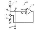
以下、PWM制御に使用される発振回路の従来例について、図4を参照して説明する。発振回路10は、第1および第2定電流回路11、12と、ヒステリシスコンパレータ13と、充放電切替えスイッチ14と、コンデンサ15とを備えている。発振回路10は、通常、例えば、DC−DCコンバータ用半導体集積回路内に構成され、コンデンサ15はこの半導体集積回路に外付けされている。第1定電流回路11は、電源VDDとノードN1間に接続され、コンデンサ15を定電流I1で充電するため定電流I1を吐き出し供給する。第2定電流回路12は、スイッチ14を介して、ノードN1と接地間に接続され、コンデンサ15を定電流I1で放電するための電流と第1定電流回路11からの定電流I1とを吸い込むために定電流I2=2×I1を供給する。コンデンサ15は、ノードN1と接地間に接続されている。また、ノードN1の電位は、三角波信号Vtとして出力されるとともに、コンパレータ13に入力される。コンパレータ13は、3入力のコンパレータであって、例えば、図5に示すように、2入力コンパレータ16、17とNOR回路18、19とで構成され、ノードN1の電位の他に、第1および第2しきい値電圧VL、VHが入力され、ノードN1の電位と各しきい値電圧VL、VHとが比較され、その結果に基づく制御信号がスイッチ14に出力される。すなわち、コンパレータ13は、ノードN1の電位が第1しきい値電圧VL以下になると、ノードN1の電位が第2しきい値電圧VH以上になるまでLレベルの制御信号をスイッチ14に出力し、ノードN1の電位が第2しきい値電圧VH以上になると、ノードN1の電位が第1しきい値電圧VL以下になるまでHレベルの制御信号をスイッチ14に出力する。スイッチ14は、Lレベルの制御信号が入力されるとOFFし、Hレベルの制御信号が入力されるとONする。
【0004】
つぎに、発振回路10の動作について説明する。ノードN1の電位が第1しきい値電圧VL以下になると、コンパレータ13からスイッチ14にLレベルの制御信号が出力され、スイッチ14はOFFし、コンデンサ15が第1定電流回路11からの電流I1によりノードN1の電位が第2しきい値電圧VH以上になるまで充電される。ノードN1の電位が第2しきい値電圧VH以上になると、コンパレータ13からスイッチ14にHレベルの制御信号が出力され、スイッチ14はONし、コンデンサ15が第2定電流回路12の電流I2=2×I1と第1定電流回路11の電流I1との差I2−I1=I1によりノードN1の電位が第1しきい値電圧VL以下になるまで放電される。そして、この充放電動作を繰り返し、ノードN1から図6に示す三角波信号Vtとして出力される。
【0005】
【発明が解決しようとする課題】
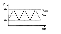
ところで、上述の発振回路10は、三角波信号Vtの周波数を高くした場合、回路内部での充放電の切替えにおける動作遅延が生じ、この動作遅延は周波数が高くなるほど増加する。そのため、図7に示すように、周波数が比較的低い場合には、三角波信号Vtの最小値VtLおよび最大値VtHは、第1および第2しきい値電圧VL、VHにほぼ一致するが、周波数を高くしていくほど、三角波信号Vtの最小値VtLが第1しきい値電圧VLより低くなっていき、最大値VtHが第2しきい値電圧VHより高くなっていく。
この発振回路10を用いて、三角波信号をDTC電圧VD maxと比較して最大オン・デューティ比を決定するとき、DTC電圧VD maxを生成するDTC回路が発振回路10と同一の半導体集積回路に構成されている場合、DTC電圧値VD maxが半導体集積回路内部で固定であり調整できない。そのため、三角波信号Vtの周波数が比較的低く、三角波信号Vtの最小値VtLおよび最大値VtHが、第1および第2しきい値電圧VL、VHにほぼ一致している間は、図6に示すように、最大オン・デューティ比が所定の適正値に設定できているが、三角波信号Vtの周波数が高くなるに従い、三角波信号Vtの振幅が大きくなり、最大オン・デューティ比が低下するという問題がある。
また、最大オン・デューティ比が一定となるように、三角波信号Vtの振幅が大きくなるのに追随させて、DTC電圧値VD maxを調整可能にするには、DTC回路を半導体集積回路の外付け回路としなければならず、半導体集積回路には、外付けのDTC回路からのDTC電圧VD maxを入力する端子と、半導体集積回路から外付けのDTC回路へ基準電圧を供給する端子とが必要となり、端子数が2個も増えるという問題がある。
本発明は三角波信号の周波数特性による最大オン・デューティ比低下を低減させた発振回路を提供することを目的とする。
【0006】
【課題を解決するための手段】
本発明に係る発振回路は、定電流で充放電するコンデンサの端子間電圧を発振信号として出力してPWM制御に用いる発振回路において、前記コンデンサが、ON/OFFスイッチを介した第1コンデンサと、第1コンデンサより容量を小さく設定した第2コンデンサとの並列回路からなり、前記端子間電圧が前記発振信号の電圧振幅の最小値と最大値間に設定した閾値電圧以上のときのみ、前記ON/OFFスイッチをOFF制御して、前記第1コンデンサのみを充放電し、このときの発振信号を用いて前記PWM制御の最大オン・デューティ比を決定することを特徴とする。
また、本発明に係る発振回路は、定電流で充放電するコンデンサの端子間電圧を発振信号として出力するために、コンデンサへの充電電流を生成する第1定電流回路と、コンデンサの放電電流を生成する第2定電流回路と、充電と放電とを切り替える充放電切替えスイッチと、前記端子間電圧を第1閾値電圧および第2閾値電圧とで比較し、第1閾値電圧以下になったら充電側に、第2閾値電圧以上になったら放電側に充放電切替えスイッチを切替える制御信号を生成する第1コンパレータとを具備したPWM制御に用いる発振回路において、前記コンデンサが、ON/OFFスイッチを介した第1コンデンサと、第1コンデンサより容量を小さく設定した第2コンデンサとの並列回路からなり、前記端子間電圧を第1閾値電圧と第2閾値電圧間に設定した第3閾値電圧で比較し、前記端子間電圧が前記第3閾値電圧以上のときのみ、前記ON/OFFスイッチをOFF制御する信号を生成する第2コンパレータを有し、このOFF制御により前記第1コンデンサのみを充放電し、このときの発振信号を用いて前記PWM制御の最大オン・デューティ比を決定することを特徴とする。
【0007】
【発明の実施の形態】
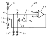
以下に、本発明に基づき第1実施例の発振回路について、図1を参照して説明する。尚、図4と同一のものについては同一符号を付している。発振回路20は、第1および第2定電流回路11、12と、ヒステリシスコンパレータ13と、充放電切替えスイッチ14とを、発振回路10と同様に、備えるとともに、コンパレータ21と、ON/OFFスイッチ22と、第1コンデンサ23と、第2コンデンサ24とを新たに備えている。発振回路20は、例えば、DC−DCコンバータ用半導体集積回路内に構成され、コンデンサ23、24はこの半導体集積回路に外付けされる。スイッチ22と第1コンデンサ23とは、ノードN1と接地間に直列に接続されている。第2コンデンサ24は、ノードN1と接地間に接続されている。第2コンデンサ24の容量CT2は、第1コンデンサ23の容量CT1より小さく設定する。コンパレータ21は、2入力のコンパレータであって、ノードN1の電位と、第3しきい値電圧VB(VL<VB<VH、VH−VB≧VB−VL)が入力され、ノードN1の電位としきい値電圧VBとが比較され、その結果に基づく制御信号がスイッチ22に出力される。すなわち、コンパレータ21は、ノードN1の電位が第3しきい値電圧VB以上になるまでHレベルの制御信号をスイッチ22に出力し、ノードN1の電位が第3しきい値電圧VB以上になるとLレベルの制御信号をスイッチ22に出力する。スイッチ22は、Hレベルの制御信号が入力されるとONし、Lレベルの制御信号が入力されるとOFFする。
【0008】
つぎに、発振回路20の動作について説明する。ノードN1の電位が第1しきい値電圧VL以下になると、コンパレータ13からスイッチ14にLレベルの制御信号が出力され、スイッチ14はOFFするとともに、このときコンパレータ21からスイッチ22にHレベルの制御信号が出力されており、スイッチ22はONし、コンデンサ23、24が第1定電流回路11からの電流I1によりノードN1の電位が第3しきい値電圧VBになるまで充電される。充電されるコンデンサ23、24は並列接続であるため、その容量の和CはC=CT1+CT2で表される。このとき、ノードN1の電位がVLからVBになるまでの充電時間T1は、T1=C×(VB−VL)/I1で表される。
ノードN1の電位が第3しきい値電圧VB以上になると、コンパレータ21からスイッチ22にLレベルの制御信号が出力され、スイッチ22はOFFし、容量CT2のコンデンサ24のみが第1定電流回路11からの電流I1によりノードN1の電位が第2しきい値電圧VHになるまで充電される。このとき、ノードN1の電位がVBからVHになるまでの充電時間T2は、T2=CT2×(VH−VB)/I1で表される。
ノードN1の電位が第2しきい値電圧VH以上になると、コンパレータ13からスイッチ14にHレベルの制御信号が出力され、スイッチ14はONするとともに、このときコンパレータ21からスイッチ22にLレベルの制御信号が出力されており、スイッチ22はOFFし、コンデンサ24のみが第2定電流回路12の電流I2=2×I1と第1定電流回路11の電流I1との差I2−I1=I1によりノードN1の電位が第1しきい値電圧VBになるまで放電される。このとき、ノードN1の電位がVHからVBになるまでの放電時間T3は、T3=CT2×(VH−VB)/I1=T2で表される。
ノードN1の電位が第3しきい値電圧VB以下になると、コンパレータ21からスイッチ22にHレベルの制御信号が出力され、スイッチ22はONし、コンデンサ23、24が第2定電流回路12の電流I2=2×I1と第1定電流回路11の電流I1との差I2−I1=I1によりノードN1の電位が第1しきい値電圧VLになるまで放電される。放電されるコンデンサ23、24は並列接続であるため、その容量の和Cは、C=CT1+CT2で表される。このとき、ノードN1の電位がVBからVLになるまでの放電時間T4は、T4=C×(VB−VL)/I1=T1で表される。
そして、この充放電動作を繰り返し、ノードN1から図2に示す三角波信号Vtとして出力される。
【0009】
以上により生成される三角波信号Vtの周期はT1+T2+T3+T4=2×(T1+T2)で表され、コンデンサ24の容量CT2をコンデンサ23の容量CT1より小さく設定することにより、T1とT2との大小関係はT1>T2で表される。この三角波信号Vtを用いてDTC電圧VD maxとの比較による最大オン・デューティ比を決定するとき、コンデンサ23、24の充放電により生成されるT1+T4=2×T1の期間より短い、コンデンサ24のみの充放電により生成されるT2+T3=2×T2の期間の三角波信号にDTC電圧VD maxを重畳させて比較する。従って、最大オン・デューティ比は、従来の三角波を用いるよりも振幅変動に対する変化率を低くすることができる。例えば、VB−VL=VH−VBとすると、T1/(T1+T2)=C/C+CT2=(CT1+CT2)/(CT1+2CT2)となり、最大オン・デューティ比は外付けのコンデンサ23、24の容量を調整することにより所望値以上にすることができる。例えば、CT2=0.4×CT1にすると(CT1+CT2)/(CT1+2CT2)=78%となり、最大オン・デューティ比は78%以上で決定できる。このとき、例えば、DTC電圧VD maxをVHとVBの中間電圧(振幅の75%の電圧)で重畳させて比較すると、最大オン・デューティ比は88%に決定される。三角波信号Vtの周波数が高くなって三角波信号Vtの振幅が大きくなった場合に、例えば、DTC電圧VD maxがVHとVBの中間電圧から(VH−VB)/4低下した電圧(振幅の62.5%)で重畳されると、最大オン・デューティ比は82%に決定され、6%低下する。従来の三角波信号を用いた場合と同一レベルで比較すると、従来の場合の最大オン・デューティ比は、振幅の75%の電圧で重畳させると、75%に決定され、振幅の62.5%で重畳されると、62.5%に決定され、12.5%低下し、従来よりも最大オン・デューティ比の低下を低減させることができる。
【0010】
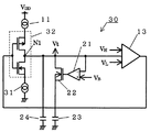
次に、本発明に基づき第2実施例の発振回路について、図3を参照して説明する。尚、図1と同一のものについては同一符号を付して、その説明を省略する。図1と異なる点は、第2定電流回路12の替わりに、コンデンサ23,24を定電流I1で放電するための電流を吸い込むために定電流I2=I1を供給する第2定電流回路31を設け、充放電切替えスイッチ14の替わりにCMOS構成の充放電切替えスイッチ32を第1定電流回路11と第2定電流回路31間に接続し、ヒステリシスコンパレータ13の出力をスイッチ32に供給し、スイッチ32の出力端をノードN1に接続している点である。この発振回路30の動作は、コンパレータ32の出力がLレベルのとき、第1定電流回路11からノードN1に定電流I1を吐き出し、Hレベルのとき、ノードN1から第2定電流回路31に定電流I2=I1を吸い込む以外は、図1の発振回路20と同様の動作であり、説明を省略する。
【0011】
尚、上記実施例では、発振回路がPWM制御されるDC−DCコンバータに用いられることを例に説明したが、PWM制御される回路で、PWM制御が最大オン・デューティ比で制限される回路であれば、他の回路にも用いることができる。
【0012】
【発明の効果】
本発明によれば、定電流で充放電するコンデンサの端子間電圧を三角波信号として出力するPWM制御に用いる発振回路において、コンデンサを第1コンデンサと、スイッチを介した第2コンデンサとの並列回路で構成し、第1コンデンサの容量を第2コンデンサの容量より小さく設定するとともに、発振信号の電圧振幅の最小値と最大値間に閾値電圧を設定し、端子間電圧が閾値電圧以上のとき、スイッチをOFF制御して、第1コンデンサのみを充放電し、このときの発振信号を用いてPWM制御の最大オン・デューティ比を決定するようにしているので、発振信号の周波数が高くなり、発振信号の振幅が大きくなっても、最大オン・デューティ比が低くなるのを低減することができる。また、発振回路を半導体集積回路で構成する場合、外付けコンデンサ用端子を従来よりも1個増やすだけで、第1コンデンサの容量と第2コンデンサの容量を調整することにより最大オン・デューティ比を外部調整できる。
【図面の簡単な説明】
【図1】 本発明の第1実施例の発振回路の回路図。
【図2】 図1の発振回路からの三角波信号の波形図。
【図3】 本発明の第2実施例の発振回路の回路図。
【図4】 従来の発振回路の回路図。
【図5】 図1、図3、および図4の発振回路に用いられるヒステリシスコンパレータの回路図。
【図6】 図4の発振回路からの三角波信号の波形図。
【図7】 図4の発振回路からの三角波信号の振幅の周波数特性
【符号の説明】
11 第1定電流回路
12、31 第2定電流回路
13 ヒステリシスコンパレータ
14、32 充放電切替えスイッチ
20、30 発振回路
21 コンパレータ
22 ON/OFFスイッチ
23 第1コンデンサ
24 第2コンデンサ[0001]
BACKGROUND OF THE INVENTION
The present invention relates to an oscillation circuit used for PWM control.
[0002]
[Prior art]
A typical example using PWM control is a DC-DC converter. This DC-DC converter compares the triangular wave signal Vt generated by the oscillation circuit with the differential voltage V EA between the output voltage and the reference voltage to determine the duty ratio of PWM control, and controls the triangular wave signal Vt to dead time control. The maximum on-duty ratio is determined in comparison with the DTC voltage V D max from the circuit (hereinafter referred to as DTC).
[0003]
Hereinafter, a conventional example of an oscillation circuit used for PWM control will be described with reference to FIG. The oscillation circuit 10 includes first and second constant
[0004]
Next, the operation of the oscillation circuit 10 will be described. When the potential of the node N1 becomes equal to or lower than the first threshold voltage VL , an L level control signal is output from the
[0005]
[Problems to be solved by the invention]
By the way, in the oscillation circuit 10 described above, when the frequency of the triangular wave signal Vt is increased, an operation delay occurs in charge / discharge switching within the circuit, and this operation delay increases as the frequency increases. Therefore, as shown in FIG. 7, when the frequency is relatively low, the minimum value Vt L and the maximum value Vt H of the triangular wave signal Vt substantially coincide with the first and second threshold voltages V L and V H. However, as the frequency is increased, the minimum value Vt L of the triangular wave signal Vt becomes lower than the first threshold voltage V L , and the maximum value Vt H becomes higher than the second threshold voltage V H. To go.
A semiconductor integrated circuit in which the DTC circuit that generates the DTC voltage V D max is the same as the oscillation circuit 10 when the maximum on-duty ratio is determined by comparing the triangular wave signal with the DTC voltage V D max using the oscillation circuit 10 In this case, the DTC voltage value V D max is fixed inside the semiconductor integrated circuit and cannot be adjusted. Therefore, while the frequency of the triangular wave signal Vt is relatively low and the minimum value Vt L and the maximum value Vt H of the triangular wave signal Vt are substantially equal to the first and second threshold voltages V L and V H , As shown in FIG. 6, the maximum on-duty ratio can be set to a predetermined appropriate value, but as the frequency of the triangular wave signal Vt increases, the amplitude of the triangular wave signal Vt increases and the maximum on-duty ratio decreases. There is a problem of doing.
Further, in order to make the DTC voltage value V D max adjustable so that the amplitude of the triangular wave signal Vt increases so that the maximum on-duty ratio becomes constant, the DTC circuit is connected to the outside of the semiconductor integrated circuit. The semiconductor integrated circuit has a terminal for inputting the DTC voltage V D max from the external DTC circuit and a terminal for supplying a reference voltage from the semiconductor integrated circuit to the external DTC circuit. There is a problem that the number of terminals increases by two.
An object of the present invention is to provide an oscillation circuit in which a decrease in maximum on-duty ratio due to frequency characteristics of a triangular wave signal is reduced.
[0006]
[Means for Solving the Problems]
An oscillation circuit according to the present invention includes an oscillation circuit that outputs a voltage between terminals of a capacitor that is charged and discharged with a constant current as an oscillation signal and is used for PWM control, wherein the capacitor includes a first capacitor via an ON / OFF switch; The ON / OFF circuit is composed only of a parallel circuit with a second capacitor having a capacitance smaller than that of the first capacitor, and the voltage between the terminals is equal to or higher than a threshold voltage set between the minimum value and the maximum value of the voltage amplitude of the oscillation signal. An OFF switch is controlled to be turned off to charge / discharge only the first capacitor, and the maximum on-duty ratio of the PWM control is determined using the oscillation signal at this time.
The oscillation circuit according to the present invention includes a first constant current circuit that generates a charging current for the capacitor, and a discharge current of the capacitor in order to output a voltage between terminals of the capacitor that is charged and discharged with a constant current as an oscillation signal. A second constant current circuit to be generated, a charge / discharge changeover switch for switching between charge and discharge, and the inter-terminal voltage are compared with the first threshold voltage and the second threshold voltage, and when the voltage falls below the first threshold voltage, the charge side In addition, in the oscillation circuit used for PWM control including a first comparator that generates a control signal for switching the charge / discharge switching switch on the discharge side when the second threshold voltage is exceeded, the capacitor is connected via an ON / OFF switch. It consists of a parallel circuit of a first capacitor and a second capacitor whose capacity is set smaller than that of the first capacitor, and the inter-terminal voltage is expressed as a first threshold voltage and a second threshold voltage. A second comparator that generates a signal for controlling the ON / OFF switch to be turned off only when the voltage between the terminals is equal to or higher than the third threshold voltage. Thus, only the first capacitor is charged and discharged, and the maximum on-duty ratio of the PWM control is determined using the oscillation signal at this time.
[0007]
DETAILED DESCRIPTION OF THE INVENTION
The oscillation circuit of the first embodiment according to the present invention will be described below with reference to FIG. In addition, the same code | symbol is attached | subjected about the same thing as FIG. The
[0008]
Next, the operation of the
When the potential of the node N1 becomes equal to or higher than the third threshold voltage V B , an L level control signal is output from the
When the potential of the node N1 becomes equal to or higher than the second threshold voltage V H , an H level control signal is output from the
When the potential of the node N1 becomes less than the third threshold voltage V B, the control signal of H level is output to the
Then, this charge / discharge operation is repeated and output from the node N1 as a triangular wave signal Vt shown in FIG.
[0009]
The period of the triangular wave signal Vt generated as described above is expressed as T1 + T2 + T3 + T4 = 2 × (T1 + T2). By setting the capacitance C T2 of the capacitor 24 to be smaller than the capacitance C T1 of the capacitor 23, the magnitude relationship between T1 and T2 is T1> T2. When determining the maximum on-duty ratio by comparison with the DTC voltage V D max using the triangular wave signal Vt, only the
[0010]
Next, an oscillation circuit according to a second embodiment of the present invention will be described with reference to FIG. In addition, the same code | symbol is attached | subjected about the same thing as FIG. 1, and the description is abbreviate | omitted. The difference from FIG. 1 is that instead of the second constant
[0011]
In the above-described embodiment, the oscillation circuit is used in a DC-DC converter that is PWM-controlled. However, the circuit is PWM-controlled, and the circuit in which PWM control is limited by the maximum on-duty ratio. If it exists, it can be used for other circuits.
[0012]
【The invention's effect】
According to the present invention, in an oscillation circuit used for PWM control that outputs a voltage between terminals of a capacitor that is charged and discharged with a constant current as a triangular wave signal, the capacitor is a parallel circuit of a first capacitor and a second capacitor via a switch. The first capacitor is set smaller than the second capacitor, the threshold voltage is set between the minimum value and the maximum value of the voltage amplitude of the oscillation signal, and when the terminal voltage is equal to or higher than the threshold voltage, the switch Since the maximum on-duty ratio of PWM control is determined using the oscillation signal at this time, only the first capacitor is charged / discharged, the frequency of the oscillation signal increases, and the oscillation signal It is possible to reduce the decrease in the maximum on-duty ratio even if the amplitude of the signal becomes larger. In addition, when the oscillation circuit is configured by a semiconductor integrated circuit, the maximum on-duty ratio can be increased by adjusting the capacitance of the first capacitor and the capacitance of the second capacitor by simply increasing the number of external capacitor terminals by one. External adjustment is possible.
[Brief description of the drawings]
FIG. 1 is a circuit diagram of an oscillation circuit according to a first embodiment of the present invention.
FIG. 2 is a waveform diagram of a triangular wave signal from the oscillation circuit of FIG.
FIG. 3 is a circuit diagram of an oscillation circuit according to a second embodiment of the present invention.
FIG. 4 is a circuit diagram of a conventional oscillation circuit.
FIG. 5 is a circuit diagram of a hysteresis comparator used in the oscillation circuits of FIGS. 1, 3, and 4;
6 is a waveform diagram of a triangular wave signal from the oscillation circuit of FIG. 4;
7 is a frequency characteristic of the amplitude of a triangular wave signal from the oscillation circuit of FIG.
DESCRIPTION OF
Claims (2)
前記コンデンサが、ON/OFFスイッチを介した第1コンデンサと、第1コンデンサより容量を小さく設定した第2コンデンサとの並列回路からなり、
前記端子間電圧が前記発振信号の電圧振幅の最小値と最大値間に設定した閾値電圧以上のときのみ、前記ON/OFFスイッチをOFF制御して、前記第2コンデンサのみを充放電し、このときの発振信号を用いて前記PWM制御の最大オン・デューティ比を決定することを特徴とする発振回路。In the oscillation circuit used for PWM control by outputting the voltage between the terminals of the capacitor charged and discharged with a constant current as an oscillation signal,
The capacitor comprises a parallel circuit of a first capacitor via an ON / OFF switch and a second capacitor having a capacitance set smaller than the first capacitor,
Only when the voltage between the terminals is equal to or higher than a threshold voltage set between the minimum value and the maximum value of the voltage amplitude of the oscillation signal, the ON / OFF switch is OFF-controlled, and only the second capacitor is charged / discharged. An oscillation circuit characterized in that a maximum on-duty ratio of the PWM control is determined using an oscillation signal at the time.
コンデンサへの充電電流を生成する第1定電流回路と、
コンデンサの放電電流を生成する第2定電流回路と、
充電と放電とを切り替える充放電切替えスイッチと
前記端子間電圧を第1閾値電圧および第2閾値電圧とで比較し、第1閾値電圧以下になったら充電側に、第2閾値電圧以上になったら放電側に充放電切替えスイッチを切替える制御信号を生成する第1コンパレータとを具備したPWM制御に用いる発振回路において、
前記コンデンサが、ON/OFFスイッチを介した第1コンデンサと、第1コンデンサより容量を小さく設定した第2コンデンサとの並列回路からなり、
前記端子間電圧を第1閾値電圧と第2閾値電圧間に設定した第3閾値電圧で比較し、前記端子間電圧が前記第3閾値電圧以上のときのみ、前記ON/OFFスイッチをOFF制御する信号を生成する第2コンパレータを有し、このOFF制御により前記第2コンデンサのみを充放電し、このときの発振信号を用いて前記PWM制御の最大オン・デューティ比を決定することを特徴とする発振回路。In order to output the voltage between the terminals of the capacitor that charges and discharges with a constant current as an oscillation signal,
A first constant current circuit for generating a charging current to the capacitor;
A second constant current circuit for generating a discharge current of the capacitor;
The charge / discharge changeover switch for switching between charge and discharge and the voltage between the terminals are compared with the first threshold voltage and the second threshold voltage. When the voltage becomes equal to or lower than the first threshold voltage, the charge side is set. In an oscillation circuit used for PWM control including a first comparator that generates a control signal for switching a charge / discharge switch on a discharge side,
The capacitor comprises a parallel circuit of a first capacitor via an ON / OFF switch and a second capacitor having a capacitance set smaller than the first capacitor;
The inter-terminal voltage is compared with a third threshold voltage set between the first threshold voltage and the second threshold voltage, and the ON / OFF switch is OFF-controlled only when the inter-terminal voltage is equal to or higher than the third threshold voltage. A second comparator for generating a signal, wherein only the second capacitor is charged / discharged by the OFF control, and the maximum on-duty ratio of the PWM control is determined using the oscillation signal at this time Oscillator circuit.
Priority Applications (1)
| Application Number | Priority Date | Filing Date | Title |
|---|---|---|---|
| JP2001387087A JP3914047B2 (en) | 2001-12-20 | 2001-12-20 | Oscillator circuit |
Applications Claiming Priority (1)
| Application Number | Priority Date | Filing Date | Title |
|---|---|---|---|
| JP2001387087A JP3914047B2 (en) | 2001-12-20 | 2001-12-20 | Oscillator circuit |
Publications (3)
| Publication Number | Publication Date |
|---|---|
| JP2003188693A JP2003188693A (en) | 2003-07-04 |
| JP2003188693A5 JP2003188693A5 (en) | 2005-03-17 |
| JP3914047B2 true JP3914047B2 (en) | 2007-05-16 |
Family
ID=27596023
Family Applications (1)
| Application Number | Title | Priority Date | Filing Date |
|---|---|---|---|
| JP2001387087A Expired - Fee Related JP3914047B2 (en) | 2001-12-20 | 2001-12-20 | Oscillator circuit |
Country Status (1)
| Country | Link |
|---|---|
| JP (1) | JP3914047B2 (en) |
Families Citing this family (8)
| Publication number | Priority date | Publication date | Assignee | Title |
|---|---|---|---|---|
| US7034586B2 (en) * | 2004-03-05 | 2006-04-25 | Intersil Americas Inc. | Startup circuit for converter with pre-biased load |
| JP2006333589A (en) * | 2005-05-25 | 2006-12-07 | Mitsumi Electric Co Ltd | Switching power supply device and its control method |
| DE112006002710B4 (en) | 2005-10-17 | 2016-02-11 | Autonetworks Technologies, Ltd. | PWM signal generator |
| DE112006002885B8 (en) | 2005-10-31 | 2016-01-14 | Autonetworks Technologies, Ltd. | Power supply controller |
| JP2008054220A (en) * | 2006-08-28 | 2008-03-06 | Rohm Co Ltd | Pulse generator, electronic device using the same and pulse generating method |
| JP6087670B2 (en) * | 2013-03-08 | 2017-03-01 | 新日本無線株式会社 | Pulse generation circuit |
| JP7206062B2 (en) * | 2018-06-19 | 2023-01-17 | 新電元工業株式会社 | Oscillator circuit and method of controlling the oscillator circuit |
| FR3082959A1 (en) | 2018-06-26 | 2019-12-27 | Stmicroelectronics (Rousset) Sas | CYCLIC CONTROL OF CELLS OF AN INTEGRATED CIRCUIT |
-
2001
- 2001-12-20 JP JP2001387087A patent/JP3914047B2/en not_active Expired - Fee Related
Also Published As
| Publication number | Publication date |
|---|---|
| JP2003188693A (en) | 2003-07-04 |
Similar Documents
| Publication | Publication Date | Title |
|---|---|---|
| US7876077B2 (en) | Control circuit and control method of current mode control type DC-DC converter | |
| JP6107358B2 (en) | Power supply circuit, power supply IC, power amplification device, and wireless communication device | |
| US7075275B2 (en) | DC-DC converter | |
| US10476309B2 (en) | Wireless power transfer system and a wireless power receiver thereof | |
| US6670779B2 (en) | High power factor electronic ballast with lossless switching | |
| KR100744592B1 (en) | Dc-dc converter, dc-dc converter control circuit, and dc-dc converter control method | |
| CN1722592B (en) | Closed-loop digital control system for a DC/DC converter | |
| US5436550A (en) | AC-DC converter having saw-tooth wave generating circuit in active filter | |
| KR100713797B1 (en) | Step-up/down dc-dc converter | |
| US20070285151A1 (en) | Power supply circuit | |
| JP4630165B2 (en) | DC-DC converter | |
| US7741887B2 (en) | Triangular wave generator | |
| TWI689161B (en) | Power converter | |
| US20130099834A1 (en) | Ramp signal generation circuit and ramp signal adjustment circuit | |
| JP3914047B2 (en) | Oscillator circuit | |
| JP2002159172A (en) | Power source and discharge lamp lighting device | |
| JP3870916B2 (en) | Sawtooth generator | |
| JP2004072657A (en) | Triangular wave oscillation circuit | |
| JP2013207895A (en) | Step-down type dc-dc converter, and portable device | |
| JP3757219B2 (en) | Charge pump circuit | |
| JP2000184612A (en) | Dc-dc converter, its control method and its control circuit | |
| KR100426606B1 (en) | DC―DC Convertor and an electronic device using the same | |
| JP6938254B2 (en) | Control method for semiconductor devices, battery monitoring systems, and booster circuits | |
| CN220775798U (en) | Capacitive switch circuit, feedback control circuit, frequency locking loop circuit, chip and electronic equipment | |
| JP7067841B2 (en) | Semiconductor device and voltage generation method |
Legal Events
| Date | Code | Title | Description |
|---|---|---|---|
| A521 | Written amendment |
Free format text: JAPANESE INTERMEDIATE CODE: A523 Effective date: 20040409 |
|
| A621 | Written request for application examination |
Free format text: JAPANESE INTERMEDIATE CODE: A621 Effective date: 20040409 |
|
| RD02 | Notification of acceptance of power of attorney |
Free format text: JAPANESE INTERMEDIATE CODE: A7422 Effective date: 20050118 |
|
| A711 | Notification of change in applicant |
Free format text: JAPANESE INTERMEDIATE CODE: A711 Effective date: 20050510 |
|
| A977 | Report on retrieval |
Free format text: JAPANESE INTERMEDIATE CODE: A971007 Effective date: 20061222 |
|
| TRDD | Decision of grant or rejection written | ||
| A01 | Written decision to grant a patent or to grant a registration (utility model) |
Free format text: JAPANESE INTERMEDIATE CODE: A01 Effective date: 20070109 |
|
| A61 | First payment of annual fees (during grant procedure) |
Free format text: JAPANESE INTERMEDIATE CODE: A61 Effective date: 20070201 |
|
| R150 | Certificate of patent or registration of utility model |
Free format text: JAPANESE INTERMEDIATE CODE: R150 |
|
| FPAY | Renewal fee payment (event date is renewal date of database) |
Free format text: PAYMENT UNTIL: 20100209 Year of fee payment: 3 |
|
| FPAY | Renewal fee payment (event date is renewal date of database) |
Free format text: PAYMENT UNTIL: 20110209 Year of fee payment: 4 |
|
| FPAY | Renewal fee payment (event date is renewal date of database) |
Free format text: PAYMENT UNTIL: 20110209 Year of fee payment: 4 |
|
| S533 | Written request for registration of change of name |
Free format text: JAPANESE INTERMEDIATE CODE: R313533 |
|
| FPAY | Renewal fee payment (event date is renewal date of database) |
Free format text: PAYMENT UNTIL: 20110209 Year of fee payment: 4 |
|
| R350 | Written notification of registration of transfer |
Free format text: JAPANESE INTERMEDIATE CODE: R350 |
|
| FPAY | Renewal fee payment (event date is renewal date of database) |
Free format text: PAYMENT UNTIL: 20110209 Year of fee payment: 4 |
|
| FPAY | Renewal fee payment (event date is renewal date of database) |
Free format text: PAYMENT UNTIL: 20120209 Year of fee payment: 5 |
|
| FPAY | Renewal fee payment (event date is renewal date of database) |
Free format text: PAYMENT UNTIL: 20130209 Year of fee payment: 6 |
|
| FPAY | Renewal fee payment (event date is renewal date of database) |
Free format text: PAYMENT UNTIL: 20140209 Year of fee payment: 7 |
|
| LAPS | Cancellation because of no payment of annual fees |