JP3913531B2 - Spacer and mounting method using the same - Google Patents
Spacer and mounting method using the same Download PDFInfo
- Publication number
- JP3913531B2 JP3913531B2 JP2001348865A JP2001348865A JP3913531B2 JP 3913531 B2 JP3913531 B2 JP 3913531B2 JP 2001348865 A JP2001348865 A JP 2001348865A JP 2001348865 A JP2001348865 A JP 2001348865A JP 3913531 B2 JP3913531 B2 JP 3913531B2
- Authority
- JP
- Japan
- Prior art keywords
- solder
- spacer
- land
- metal
- bga package
- Prior art date
- Legal status (The legal status is an assumption and is not a legal conclusion. Google has not performed a legal analysis and makes no representation as to the accuracy of the status listed.)
- Expired - Fee Related
Links
Images


Classifications
-
- H—ELECTRICITY
- H01—ELECTRIC ELEMENTS
- H01L—SEMICONDUCTOR DEVICES NOT COVERED BY CLASS H10
- H01L2224/00—Indexing scheme for arrangements for connecting or disconnecting semiconductor or solid-state bodies and methods related thereto as covered by H01L24/00
- H01L2224/73—Means for bonding being of different types provided for in two or more of groups H01L2224/10, H01L2224/18, H01L2224/26, H01L2224/34, H01L2224/42, H01L2224/50, H01L2224/63, H01L2224/71
- H01L2224/732—Location after the connecting process
- H01L2224/73201—Location after the connecting process on the same surface
- H01L2224/73203—Bump and layer connectors
- H01L2224/73204—Bump and layer connectors the bump connector being embedded into the layer connector
-
- H—ELECTRICITY
- H01—ELECTRIC ELEMENTS
- H01L—SEMICONDUCTOR DEVICES NOT COVERED BY CLASS H10
- H01L2224/00—Indexing scheme for arrangements for connecting or disconnecting semiconductor or solid-state bodies and methods related thereto as covered by H01L24/00
- H01L2224/80—Methods for connecting semiconductor or other solid state bodies using means for bonding being attached to, or being formed on, the surface to be connected
- H01L2224/83—Methods for connecting semiconductor or other solid state bodies using means for bonding being attached to, or being formed on, the surface to be connected using a layer connector
- H01L2224/831—Methods for connecting semiconductor or other solid state bodies using means for bonding being attached to, or being formed on, the surface to be connected using a layer connector the layer connector being supplied to the parts to be connected in the bonding apparatus
- H01L2224/83101—Methods for connecting semiconductor or other solid state bodies using means for bonding being attached to, or being formed on, the surface to be connected using a layer connector the layer connector being supplied to the parts to be connected in the bonding apparatus as prepeg comprising a layer connector, e.g. provided in an insulating plate member
Landscapes
- Electric Connection Of Electric Components To Printed Circuits (AREA)
- Structures For Mounting Electric Components On Printed Circuit Boards (AREA)
- Wire Bonding (AREA)
- Encapsulation Of And Coatings For Semiconductor Or Solid State Devices (AREA)
Abstract
Description
【0001】
【発明の属する技術分野】
本発明は、高密度かつ小型化が要求される半導体のパッケージング、高性能且つ高機能化及び小型携帯化が急速に進んでいる携帯電話、および、ビデオカメラ等のモバイル電子機器に関し、詳しくは、これらからの要求によりさらなる高密度で軽薄短小なエリア実装技術及びエリア実装装置など広範なニーズに対応可能な構造体及びその構造体を用いた実装方法に関する。
【0002】
【従来の技術】
従来のエリア実装方式の一種であるリフロー実装について図6に基づき説明する。図6(a)のように、プリント回路基板101上には、半導体パッケージの一種であるBGAパッケージ106(Ball・Grid・Array)のソルダーバンプ105に対応するようにランド102が形成されている。BGAパッケージのソルダーバンプ105とプリント回路基板上のランド102を半田接合させるエリア実装では、初めに、マスクを用いたスクリーン印刷によって、マスクの開口部から半田ペースト103がランド102の上部に印刷される。
【0003】
この時、半田ペースト103の印刷量はマスクの開口部の形状、マスク厚さ、及び半田ペースト103を印刷するスキージ速度の管理などでコントロールしているが、安定且つ定量的に半田ペースト103の印刷量を保つまでには至っていない。次工程での半田接合不良の発生は、半田ペースト103の印刷状態に起因する為、半田ペースト103を印刷した後で、その印刷状態を外観的に検査する必要がある。このような外観検査は、BGAパッケージ106がプリント回路基板101に実装された時、半田接合部分がBGAパッケージ101の裏側に隠れてしまうような場合、すなわち、実装後に半田接合の不良を外観で発見することが困難な場合に特に必要になる。
【0004】
図7(a)は、半田ペースト103の印刷量にバラツキが発生した時の半田接合不良の第1の状態図である。半田ペースト103がランド102上に印刷された形状が高さ方向にて十分でなく、且つ半田ペースト103印刷量が足りないために半田接合が不十分になり、導通不良が発生する。
【0005】
これは、プリント回路基板101上のランド102形状を小さくすると同時にマスクの開口寸法を小さくする為、印刷形状が円錐形状となりランド102に対する印刷面積は良品と同程度であっても半田ペースト103印刷量が不十分になることからソルダーバンプ105とランド102間が導通不良になる。
【0006】
上記の導通不良は、全ランド102の印刷状態の中で、ある一部のランド102だけに発生するため検出が困難である。
【0007】
さらに半田接合が不十分な状態にて、プリント回路基板101に何らかの外的衝撃が加わった時に、半田接合部分が破断して二次的な導通不良を発生させる。
【0008】
図7(b)は、半田ペースト103の印刷量のバラツキにより生じる半田接合不良を示す状態図である。ランド102の面積に対して半田ペースト103を多めに印刷したために、ランド102から半田ペースト103がはみ出した状態になり、隣接するランド102間にてショートし導通不良になる。量産作業では、半田ペースト103印刷量が安定しない要因として使用されているマスクとスキージの繰り返し作業による接触部での磨耗現象によるものである。よって、マスク開口形状及びスキージ形状が変形し、印圧が変化する事で半田ペースト103印刷量が安定しなくなる。さらに、半田ペースト103印刷量が安定しない要因として、半田ペースト103の印刷工程を繰り返し実施していくと、マスク開口部に半田ペースト103が付着、残存し、やがて固着してしまう為である。
よって、マスク開口部とランドとの密着性が損なわれて半田ペースト103印刷量が安定しない。上記の要因は、微細なランド102への半田ペースト103印刷であるほど発生する。よって、微細なランド102の半田ペースト103印刷にはスキージ速度の管理及びマスク開口部からの半田ペースト103の抜け性を確保する必要がある。
【0009】
図7(c)は、半田ペースト103の印刷量にバラツキが発生した時の半田接合不良を示す状態図である。BGAパッケージ106の接合端子のピッチが従来の0.8mmから0.5mm、0.3mm、さらにそれ以下にファイン化されると半田ペースト103の印刷量を確保するために、半田粒子も同様に小径に推移せざるを得ない。これは、微細なマスク開口部に対して半田ペースト103の抜け性を確保し、安定的に半田ペースト103量を印刷するためである。
【0010】
尚、半田ペースト103の抜け性は、マスク開口部の面積に対して半田粒子が最低5粒子並ぶ位を目安としている。半田粒度を小さくすることは、半田粒子の充填密度が上がり総粒子の表面積は、大きくなるため粒子一個当りのフラックス量は減少する事となる。よって、半田粒子及びフラックスの酸化は従来よりも速くなる。酸化された半田粒子と被酸化半田粒子とが混在した状態にて半田接合を実施した場合、半田粒子個々の溶融温度にバラツキが発生し、フィレット形成が出来なかった半田粒子がソルダーボール108として発生する。この固着していないソルダーボール108がプリント回路基板101のランド102周辺に発生することにより、隣接するランド102間にてショートされ導通不良となる。
【0011】
図6(b)のように、BGAパッケージ106のグリットアレイ形状に配列された端子104上にソルダーバンプ105が形成されている。ソルダーバンプ105と半田ペースト103を印刷したプリント回路基板101のランド102とを位置合わせしながら載せる。尚、BGAパッケージの端子104径とプリント回路基板101のランド102径の関係は、1:1にて対応するのが通常となっている。
【0012】
図8(a)は、ソルダーバンプ105とランド102の搭載のバラツキによる半田接合不良の第1の状態図である。これは、BGAパッケージ106を搭載した時に、BGAパッケージの端子104であるソルダーバンプ105が所定のランド102と位置がずれて、搭載された場合を示す。この時、ソルダーバンプ105とランド102の位置ズレによって、隣接するランド102間にてショートされ導通不良となる。
【0013】
図8(b)は、ソルダーバンプ105とランド102の搭載のバラツキによる半田接合不良の第2の状態図である。これは、ランド102上の半田ペースト103量が多い場合、BGAパッケージ106を搭載した時の衝撃力にて塗布されていた半田ペースト103が飛び散ることによりソルダーボール108が発生する。この原因によって、隣接するランド102間にてショートされ導通不良となる。
【0014】
次に図6(c)のように、ソルダーバンプ105とプリント回路基板101のランド102とが接触された状態にて、リフロー装置に流動される。リフロー装置内にて、ソルダーバンプ105とランド102上の半田ペースト103とが溶融化され半田接合される。通常のリフロー半田接合方式としては、まずリフロー装置を一定温度まで上昇させる。さらに、プリヒート工程にてプリント回路基板101及びBGAパッケージ106の表面温度を均一化させる。上記のプリヒートの加熱時間を必要以上に実施した場合は、図8(b)のようなソルダーボール108が発生する。また、プリヒートの温度を急激に上昇させた場合も同様にソルダーボール108等の実装不良が発生する。その後、半田溶融温度まで加熱させ、半田が溶融化する。その際、ソルダーバンプ105及び半田ペースト103が溶融化した状態にて、半田自身の表面張力がセルフアライメント効果を発生させ所定のランド102へ半田接合することができる。
【0015】
BGAパッケージ106の表面温度とソルダーバンプ105の温度は、BGAパッケージ106のサイズによって差が生じるため、BGAパッケージ106のサイズ違いを混載実装する場合には、各BGAパッケージ106の耐熱温度範囲内で十分な半田接合性が得られるような半田接合条件を設定する必要がある。また、近年、鉛レス半田が採用され、その半田組成は単一金属がその成分の90%を占めており、従来のSn-Pb半田よりも半田流動性が劣っており、前記セルフアライメント効果が低下する。さらにまた、鉛レス半田は、従来の半田温度では溶融接合できない高温域での接合条件となる為、BGAパッケージ106の端子及び他電子部品等の耐熱性が問題となる。その為、鉛レス半田の溶融温度と部品耐熱温度の範囲内にて半田接合性を確保する必要がある。
【0016】
次に図6(d)のように、BGAパッケージ106とプリント回路基板101との隙間に、アンダーフィル材107と称される樹脂材を流し込む。上記のアンダーフィル材107を塗布することにより、外部からの応力等が半田接合部に加わった場合に半田接合部の不良を発生させないための応力緩和及び保護を目的とする。その後、流し込まれるアンダーフィル材107には、熱硬化型の樹脂を使用するのが一般的であり、その熱硬化に適した加熱条件にて処理させることにより、樹脂が硬化される。今後のBGAパッケージ106は、小面積且つ要求仕様を満足させるための入出力端子の多ピン化及びそれに対応した端子のファインピッチ化の方向に進んでいる。上記のBGAパッケージ106の要求に対し、エリア実装専用のリフロー装置が必要となってくる。
【0017】
【発明が解決しようとする課題】
従来のBGAパッケージによるエリア実装においては、下記の課題があった。(1)半田ペーストの印刷精度のバラツキが、半田接合性に影響し実装不良となる。
(2)半田ペースト印刷工程を量産した時に、マスク開口部に半田ペーストが固着していくため、ランドとマスク開口部との密着性が損なわれる。
(3)半田粒子を小さくすることにより酸化する速度が速くなる。この酸化の影響により、ソルダーボールが発生する。
(4)鉛レス半田の採用により、限られた温度範囲内にて半田接合性を確保する必要がある。
【0018】
そこで、本発明はこれらの課題を解決して、下記を実現しようとするものである。
(1)BGAパッケージの多ピンに対応した高密度のエリア実装の半田接合性を確保する。
(2)半田ペーストの印刷精度に影響さらずに、半田接合性を確保する。
(3)半田粒子の酸化が発生しにくいプロセスにて、半田接合性を確保する。
(4)半田接合部を封止することにより、外部応力等による半田不具合を緩和及び保護させる。
【0019】
【課題を解決するための手段】
上記課題を解決するために、本発明の構造体は、素子のソルダーバンプと回路基板との間に設けられるスペーサーであって、加熱によりアンダーフィル機能の役割をする基材を備え、前記基材には素子に設けられたソルダーバンプの配置に対応するように貫通孔が設けられることとした。また、本発明による実装方法は、回路基板に設けられたランドの上に半田ペーストを設ける工程と、素子に設けられたソルダーバンプと、ソルダーバンプと対応する位置に貫通孔が設けられたスペーサーと、ランドとの位置が合うように貼り合せる工程と、ソルダーバンプを加熱することにより、ソルダーバンプを溶かしてランド上の半田ペーストと溶融一体化する工程とを有することとした。また、回路基板に設けられたランドの上に半田ペーストを設ける工程と、素子に設けられたソルダーバンプと、ソルダーバンプと対応する位置に貫通孔が設けられるとともに貫通孔の少なくとも一部に金属が設けられたスペーサーと、回路基板を、貫通孔の金属と前記ソルダーバンプが接触するように位置を合わせて貼り合せる工程と、ソルダーバンプを加熱することにより、前記ソルダーバンプを溶かして金属及び半田ペーストを溶融一体化する工程と、を備える実装方法とした。さらに、スペーサーを加熱することによりスペーサーを溶かして半田接合箇所に流れ出させる工程と、スペーサーを熱硬化する工程とを有することにより、ソルダーバンプとランドの半田接合箇所を封止することとした。
【0020】
本発明の参考例のスペーサー(第1の構成)は、基材と該基材に半導体素子のパッケージであるBGAパッケージのソルダーバンプの配置にホールを貫通させた貫通孔にて構成されたスペーサーであり、このスペーサーを該ソルダーバンプとプリント回路基板の間に挟み込むことにより該スペーサーが該ソルダーバンプのマスク機能を果たし、且つ加熱することによりアンダーフィル機能の役割をする。
【0021】
この発明のスペーサーの第2の構成として、前記第1の構成のスペーサーの前記貫通孔の少なくとも一部分に金属が塗布されるスペーサーとした。
【0022】
この発明のスペーサーの第3の構成として、前記第2の構成のスペーサーの前記金属として、金属有機化合物を有するスペーサーとした。
【0023】
この発明の参考例では、BGAパッケージのソルダーバンプとプリント回路基板に配線されたランドとを、前記第1の構成のスペーサーを用いて接続させる方法として、ランド上にスクリーン印刷法を用いて半田ペーストを印刷する工程と、次に貫通孔及びプリント回路基板に配線されたランド及びソルダーバンプを位置を合せて貼り合せる工程と、更に該ソルダーバンプに熱源を供給させる工程と、加熱により該ソルダーバンプが溶かされ、該ランド上の半田ペーストと溶融一体化する工程とを有する実装方法とした。
【0024】
この発明は、第1の構成のスペーサーを用いた実装手段であって更に、ソルダーバンプとランドの半田接合箇所を封止する実装方法として、該スペーサーに熱源を供給させる工程と、加熱によりスペーサーが溶けて前記半田接合箇所に流れ出す工程と、該スペーサーが熱硬化される工程とを有する実装方法とした。
【0025】
この発明は、BGAパッケージのソルダーバンプとプリント回路基板に配線されたランドとを前記第2〜3の構成のスペーサーを用いて接続させる実装方法の第1手段として、該ランド上にスクリーン印刷法を用いて半田ペーストを印刷する工程と、次に貫通孔内の金属塗布箇所とソルダーバンプが接触状態にて、プリント回路基板に配線されたランドと位置を合せて貼り合せる工程と、更に該ソルダーバンプに熱源を供給させる工程と、加熱によりソルダーバンプが溶かされ金属及び該ランド上の半田ペーストとが溶融一体化する工程とを有する実装方法とした。
【0026】
この発明は、第2〜3の構成のスペーサーを用いた実装手段であって更に、ソルダーバンプとランドの半田接合箇所を封止する実装方法として、該スペーサーに熱源を供給させる工程と、加熱によりスペーサーが溶けて前記半田接合箇所に流れ出す工程と、該スペーサーが熱硬化される工程とを有する実装方法とした。
【0027】
この発明は、第1〜3の構成のスペーサーを用いた実装手段であって更に、ソルダーバンプとランドの半田接合箇所を封止する実装方法として、BGAパッケージとプリント回路基板との隙間にアンダーフィル材を塗布する工程と、アンダーフィル剤が熱硬化される工程とを有する実装方法とした。
【0028】
【発明の実施の形態】
本発明のスペーサーは、基材に半導体素子のパッケージであるBGAパッケージのソルダーバンプの配置に貫通孔が構成されたスペーサーである。このスペーサーを使用して、BGAパッケージに形成されているソルダーバンプとプリント回路基板に配線されたランドとを半田接合させる実装プロセスとしては、マスクをプリント回路基板上に装着し、該マスクの上から半田ペーストを塗り込ませることにより、マスクに開けた穴の開口部よりプリント回路基板に配線されたランド上に半田ペーストが印刷される。次に、半田ペーストが印刷された該ランドの位置と、本発明であるスペーサーに設けられた貫通孔の位置とが合わさった状態にて本発明品のスペーサーをプリント配線基板に貼り合せる。さらに、貫通孔の位置と、BGAパッケージに形成されている各ソルダーバンプの位置とが合わさった状態にてスペーサー上にBGAパッケージを搭載する。BGAパッケージの上部より加圧することにより、ソルダーバンプがスペーサーの貫通孔内輪に挿入された図2(b)のような状態になる。
【0029】
本発明のスペーサーは、微細形状の貫通孔が個々のランドに分断させる枠組みの役割を果たす。要するに、ランド上の半田ペーストが個々に隔離され、該スペーサーの上にBGAパッケージ端子のソルダーバンプを存在させることで半田接合の為の閉ざされた空間を確立する事ができる。
【0030】
次に、上記の貼り合わさった状態にてリフロー装置内に流動し、プリヒートによりBGAパッケージ及びプリント回路基板を加熱させる。この時、BGAパッケージに形成されている端子を介してソルダーバンプも加熱され、尚且つプリント回路基板のランドを介して半田ペーストも加熱される。リフロー装置の温度設定は、ソルダーバンプが溶融する温度まで上昇させる。溶融温度にて加熱されたソルダーバンプは溶融化され、前記スペーサーの貫通孔の内部にてランド上の半田ペーストと接触し、溶融一体化される。本発明によるスペーサーの貫通孔の範囲内にて半田接合されるため、隣接しているランドから隔離でき、確実な半田接合を実施することが出来る。
【0031】
次に、リフロー装置を該スペーサーが溶解する温度まで上昇させる。半田溶融温度にて加熱された該スペーサーは溶解化し、その後に熱硬化する。本発明のスペーサーは、外部からの応力等が半田接合部に加わった場合に半田接合部の不良を発生させないための応力緩和及び保護を目的とする。これは、プリント回路基板を搭載した製品が落下により衝撃ストレスを受けた場合、このストレスはBGAパッケージとその半田接合部に集中することになる。BGAパッケージの半田接合部は、QFPパッケージのようなリードフレームを持たないため、一番弱い箇所に応力が集中し接合部周辺で破壊が発生する。要するに、半田接合部の周辺を本発明のスペーサーにて固定させ保護することにより、強度アップが図れる。さらに、本発明のスペーサー自体がアンダーフィル材の役割を兼ね備えているので、製造工程への負担が減少できる。上述のスペーサーの貫通孔のグリットアレイ配列に関しては、BGAパッケージのソルダーバンプの配列によって決定される。BGAパッケージのソルダーバンプの配列は、入出力仕様及びサイズ等により端子数が異なり、限られた面積内に多くの端子を配列させている。よって、本発明のスペーサーの貫通孔をBGAパッケージの仕様に合わせて配列させることにより、多品種なBGAパッケージに使用することができる。
【0032】
さらに、本発明のスペーサーを使用した半田接合プロセスに於いて、貫通孔の開口率とソルダーバンプとの関係は非常に重要である。要するに、貫通孔の開口率で枠取りされた範囲内にて、ソルダーバンプを半田接合させる実装プロセスである。上記のような第2構成のスペーサーに於いては、該貫通孔の内輪部の少なくとも一部分に金属が塗布した構成のスペーサーである。このスペーサーを用いて、BGAパッケージに形成されているソルダーバンプとプリント回路基板に配線されたランドとを半田接合させる。
【0033】
実装プロセスとしては、マスクをプリント回路基板上に装着し、該マスクの上から半田ペーストを塗り込ませることにより、マスク板に開けた穴の開口部よりプリント回路基板に配線されたランド上に半田ペーストが印刷される。
【0034】
次に、半田ペーストが印刷された該ランドの位置と、本発明であるスペーサーに設けられた貫通孔の内輪に形成されている金属の位置とが合わさった状態にて本発明品のスペーサーをプリント配線基板に貼り合せる。さらに、前記貫通孔の金属の位置と、BGAパッケージに形成されているソルダーバンプの位置とが合わさった状態にてスペーサー上にBGAパッケージを搭載する。
【0035】
本発明のスペーサーは、微細形状の貫通孔が個々のランドに分断させる枠組みの役割を果たす。要するに、ランド上の半田ペーストが個々に隔離され、該スペーサーの上にBGAパッケージ端子のソルダーバンプを存在させることで半田接合の為の閉ざされた空間を確立することができる。
【0036】
さらに、前記BGAパッケージの上部より加圧することにより、該ソルダーバンプが該スペーサーの貫通孔内輪に形成されている金属部が接触された状態になる。本発明のスペーサー内の該金属と前記ソルダーバンプとを接触させることにより、個々の表面に形成されている酸化膜を破壊することになる。よって、該金属と該ソルダーバンプとの接触部分は、導通性及び熱伝導性が良くなって、確実な半田接合を実施することが出来る。
【0037】
次に、貼り合わさった状態にてリフロー装置内に流動し、プリヒートによりBGAパッケージ及びプリント回路基板を加熱させる。この時、BGAパッケージに形成されている端子を介してソルダーバンプも加熱され、さらにプリント回路基板のランドを介して半田ペーストも加熱される。リフロー装置の温度設定をソルダーバンプが溶融する温度まで上昇させる。溶融温度にて加熱されたソルダーバンプは溶融化され、スペーサーの貫通孔内輪の金属と合金化反応を起し、ソルダーバンプと金属は金属溶融接合される。さらに、金属溶融接合されたソルダーバンプ及び金属は、スペーサーの貫通孔内部にてランド上の半田ペーストと接触し、溶融一体化される。本発明によるスペーサーの貫通孔の範囲内にて半田接合されるため、隣接しているランドから隔離でき、確実な半田接合を実施することが出来る。これは、貫通孔の限られた範囲にて半田接合を実施する事は、余分な半田ペーストが隣接するランドに流れ込むことを防ぐのに都合がよい。
【0038】
さらに、半田ペースト内のフラックスは、スペーサーによって個々にランドとソルダーボールを一対で隔離している為、環境温度が上昇する事で確実にソルダーボールに付着することができる。
【0039】
よって、環境温度が上がることにより、プリント回路基板上のランドに熱が伝わって半田ペーストの活性化が良くなり、確実な半田接合を実施することが出来る。環境温度を上げる手段としては、プリント回路基板側から加熱する方法があるが、本発明のスペーサーを使用することにより同様の効果を得られることとなる。次に、リフロー装置を該スペーサーが溶解する温度まで上昇させる。半田溶融温度にて加熱された該スペーサーは溶解し、その後に熱硬化する。本発明のスペーサーは、外部からの応力等が半田接合部に加わった場合に、半田接合部の不良を発生させないための応力緩和及び保護を目的とする。さらに、本発明のスペーサー自体がアンダーフィル材の役割を兼ね備えているので、製造工程への負担が減少できる。
【0040】
本発明のスペーサーに形成する金属を薄膜形状にすることにより、該ソルダーバンプと金属部の接触範囲が安定する。それにより、接触部分の導電性及び熱伝導性が安定的に良くなり、確実な半田接合を実施することが出来る。
【0041】
さらに、従来技術にて半田接合不良の原因であった、半田ペーストの印刷量のバラツキを改善するために、半田溶融化する金属の厚みにてランド面積に対する半田量を代用して、半田ペースト側は予備半田程度に抑えることにより、確実な半田接合を実施することが出来る。
【0042】
さらに、図4は貫通孔の内輪に金属及び該金属上に半田フラックスを塗布した構成のスペーサーである。金属の内輪にフラックスを塗布することにより、金属の酸化防止及び半田塗れ性の維持などの役割を果たす。プリント回路基板のランド表面にプリフラックッスを塗布することにより、ランドの酸化防止及び半田塗れ性の維持などの役割を果たす。さらにまた、本発明の実装プロセスにて、ランド上の表面状態のバラツキは非常に重要であり、プリフラックスを塗布させることによりソルダーボールの防止、及び、ランド上の半田接合性を確保するための補助手段になる。さらに、金属はBGAパッケージの耐熱温度より低く溶融する材質にする必要がある。要するに、実装プロセスに於いてリフロー装置内でBGAパッケージの樹脂が加熱される環境が発生ために、金属部分が溶融される温度をBGAパッケージの耐熱温度より低く設定する必要がある。よって、本発明の実装プロセスの最大加熱温度を、BGAパッケージの耐熱温度以下とする。
【0043】
上述した第3構成のスペーサーに於いては、金属として、金属有機化合物を焼成させて形成した金属化合物及び金属単体を使用する構成のスペーサーである。本発明の実装プロセスで要求される金属の特徴としては、半田ペースト及びソルダーバンプとの溶融性が良好で且つ半田と同一成分が含まれていること。そこで、スズ、銀、亜鉛、銅、ビスマス等を主成分とした金属化合物及び金属単体が本発明の金属として例示できる。さらに、上記スペーサーに於いては、前記基材に方向性の意味を持ったアライメントマークを形成する必要がある。本発明の実装プロセスに於いて、BGAパッケージ及びスペーサー及びプリント回路基板との方向性を考慮しなければならない。よって、基材にスペーサーの方向性を持たせたアライメントマークを取り付けることで、位置ズレ等を防止することが可能となる。
【0044】
【実施例】
以下図面に基づいて本発明の実施例を説明する。
【0045】
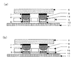
本発明による第1〜3構成のスペーサー5の断面構成を図1に示す。スペーサー5は、基材1に貫通孔2が設けられた構造である。貫通孔2は半導体素子のパッケージであるBGAパッケージのソルダーバンプ8の配置に対応するように基材1に設けられている。基材1は熱硬化性の樹脂であり、熱及び湿度による膨張性、収縮性が少なく吸湿性が低い特性を持っている。さらに基材1は、加熱されることにより接着力が増す特徴を持っている。図1(a)は基材1の構成の断面構成図である。
【0046】
図1(b)は、基材1が、ポリイミド等をベースに前述の特徴を持つ熱硬化性樹脂を背面処理した構成である場合を示している。貫通孔2は、基材1に対して円錐形状のホールを開けたものである。貫通孔2の配列は、グリットアレイ形状に構成されている。貫通孔2の加工手段としては、メカニカルに貫通させる手段または溶剤により溶かす手段さらにレーザー加工手段がある。貫通孔のグリットアレイの配列としては、ソルダーバンプ8配列の座標を元にして、基材1に貫通孔2を設けることにより多品種なBGAパッケージ6にスペーサー5を活用できる。貫通孔2の開口率としては、ソルダーバンプ8の球径によって違いがある。BGAパッケージ6に形成されているソルダーバンプ8は、限られたパッケージエリアに多ピンの入出力信号を配線している。
【0047】
ソルダーバンプ8の球径に合わせて貫通孔2の開口率を決定することにより多品種なBGAパッケージ6にスペーサー5を活用できる。本発明の第2構成のスペーサーとして、該貫通孔2の内輪部の少なくとも一部分に金属が塗布した構成になっている。金属4を貫通孔2に塗布させる手段として、ディスペンサーにより金属4を個々の貫通孔2に対して塗布する。その後、スペーサー5全体を焼成することにより、貫通孔2の少なくとも一部分に金属4が塗布される。この時、金属が焼成されることにより有機成分が乾燥され、貫通孔2の内輪部分に薄膜形状に塗布される事となる。さらに、貫通孔2に対して金属4を塗布後にフラックッス材14を塗布する構成がある。
【0048】
図4(a)のように、スペーサー5に形成する金属4の内輪にフラックス14を塗布することにより、金属4の酸化防止及び半田塗れ性の維持などの役割を果たす。
【0049】
図4(b)のように、プリント回路基板11のランド10表面にプリフラックッス15を塗布することにより、ランド10の酸化防止及び半田塗れ性の維持などの役割を果たす。ランド10上の表面状態のバラツキは非常に重要であり、プリフラックス15を塗布することによりソルダーボールの防止、及び、ランド10上の半田接合性の確保するための補助手段になる。金属4の溶融化する温度として、BGAパッケージ6表面が加熱され、表面樹脂の形状変化が発生する耐熱温度より低い溶融温度にて溶融化する材質を選定することにより、多品種なBGAパッケージ6にスペーサー5を活用できる。
【0050】
本発明の第3構成のスペーサーとして、金属4を金属有機化合物から焼成させて形成した金属化合物及び金属単体を使用する構成となっている。金属4としては、スズ、銀、亜鉛、銅、ビスマス等を主成分とした金属化合物及び金属単体である。金属4の主成分としては、半田ペースト材9と同等の溶融温度特性をもっているのが好ましい。さらに、図1のように、スペーサー5の一角に切り欠きを設けることにより、BGAパッケージ6及びプリント回路基板11との搭載する向きを合わせることが可能となる。本発明の第1構成のスペーサー5を使用した実装プロセスの第1の実施例を以下に記載する。
【0051】
図5(a)のように、プリント回路基板11とマスク16を張り合わせ、マスク16上の半田ペースト9をスキージ17により矢印18方向に移動させることにより、マスク16の開口部より半田ペースト9が押し出され、プリント回路基板11に配線されているランド10上に印刷される。
【0052】
次に、図5(b)のように、スペーサー5に設けられたアライメントマーク3を、アライメントマーク認識手段19により読み取ってスペーサー5とプリント回路基板11とを貼り合せる。この時、半田ペースト9が印刷されたランド10の位置と、スペーサー5に設けられた貫通孔2の位置とが合わさった状態にて貼り合せる。さらに、スペーサー5に設けられたアライメントマーク3を、アライメントマーク認識手段19により読み取ってスペーサー5とBGAパッケージ6を貼り合せる。
【0053】
図2(a)は、本発明の第1構成のスペーサー5の状態図である。上記の工程にて、BGAパッケージ6とスペーサー5及びプリント回路基板11が貼り合わさった状態である。この時のスペーサー5は、微細形状の貫通孔2が個々のランド10に分断させる枠組みの役割を果たす。
【0054】
次に、図5(c)で示すように、加圧手段20により矢印21方向に加圧することにより、ソルダーバンプ8がスペーサー5の貫通孔2内輪に挿入された状態になる。
【0055】
図2(b)は、本発明の第1構成のスペーサー5の状態図である。上記の工程にて、ランド10上の半田ペースト9が個々に隔離され、スペーサー5の上にBGAパッケージ端子7のソルダーバンプ8を存在させることで半田接合の為の閉ざされた空間の形態を確立できる。
【0056】
次に、図5(d)のように、BGAパッケージ6とスペーサー5及びプリント回路基板11が貼り合わさった状態で、搬送手段25により加熱手段22に流動される。さらに、加熱温度制御手段23によりプリヒートの温度まで上昇させ、BGAパッケージ6及びプリント回路基板11を加熱させる。加熱手段22としては、リフロー炉に流動させ環境温度を上昇させる方式及びリフロー炉に流動させスポット的にエアーを吹付けるエアーリフロー方式及び温風を直接吹付ける温風供給方式がある。
【0057】
図2(c)は、本発明の第1構成のスペーサー5の状態図である。上記の工程にて、BGAパッケージ端子7を介してソルダーバンプ8も加熱され、尚且つプリント回路基板11のランド10を介して半田ペースト9も加熱される。次に、加熱温度制御手段23によって、ソルダーバンプ8が溶融する温度まで上昇させる。
【0058】
図2(d)は、本発明の第1構成のスペーサー5の状態図である。上記の工程にて、溶融温度にて加熱されたソルダーバンプ8は溶融化され、スペーサー5の貫通孔2の内部にてランド10上の半田ペースト9と接触し、溶融一体化される。スペーサー5の貫通孔2の範囲内にて半田接合されるため、隣接しているランド10から隔離でき、確実な半田接合を実施することが出来る。
【0059】
次に、図5(e)のように、加熱温度制御手段23によって、スペーサー5が溶融する温度まで上昇させる。
【0060】
図2(e)は、本発明の第1構成のスペーサー5の状態図である。上記の工程にて、溶融温度に加熱されたスペーサー5は熱容量に反応してマスク形状を崩しながら、BGAパッケージ6とプリント回路基板11の空間に流れ込み、その後に熱硬化する。スペーサー5は、外部からの応力等が半田接合部に加わった場合に半田接合部の不良を発生させないための応力緩和及び保護を目的とする。さらに、スペーサー5自体がアンダーフィル材の役割を兼ね備えているので、製造工程への負担が減少できる。尚、図2(d)の状態から、アンダーフィル材をBGAパッケージ6の周辺に塗布し、再度熱処理を実施し、硬化させる方法も好ましい。
【0061】
本発明の第2および第3構成のスペーサー5を使用した実装プロセスの第2の実施例を以下に記載する。図5(a)のように、プリント回路基板11とマスク16を張り合わせ、マスク16上の半田ペースト9をスキージ17により矢印18方向に移動させることにより、マスク16の開口部より半田ペースト9が押し出され、プリント回路基板11に配線されているランド10上に印刷される。次に、図5(b)のように、スペーサー5に設けられたアライメントマーク3を、アライメントマーク認識手段19により読み取ってスペーサー5とプリント回路基板11とを貼り合せる。この時、半田ペースト9が印刷されたランド10の位置と、スペーサー5に設けられた貫通孔2の内輪に形成されている金属4の位置とが合わさった状態にて貼り合せる。この時、半田ペースト9が印刷されたランド10の位置と、スペーサー5に設けられた貫通孔2の位置とが合わさった状態にて貼り合せる。さらに、スペーサー5に設けられたアライメントマーク3を、アライメントマーク認識手段19により読み取ってスペーサー5とBGAパッケージ6を貼り合せる。
【0062】
図3(a)は、本発明の第2〜3構成のスペーサー5の状態図である。上記の工程にて、BGAパッケージ6とスペーサー5及びプリント回路基板11が貼り合わさった状態である。この時のスペーサー5は、微細形状の貫通孔2が個々のランド10に分断させる枠組みの役割を果たす。次に、図5(c)のように、加圧手段20により矢印21方向に加圧することにより、ソルダーバンプ8がスペーサー5の貫通孔2内輪に挿入された状態になる。
【0063】
図3(b)は、本発明の第2〜3構成のスペーサー5の状態図である。上記の工程にて、ランド10上の半田ペースト9が個々に隔離され、スペーサー5の上にBGAパッケージ端子7のソルダーバンプ8を存在させることで半田接合の為の閉ざされた空間を確立する事ができる。さらに、BGAパッケージ6の上部より加圧することにより、ソルダーバンプ8がスペーサー5の貫通孔2内輪に形成されている金属4部が接触された状態になる。スペーサー5内の金属4とソルダーバンプ8とを接触させることにより、個々の表面に形成されている酸化膜を破壊することになる。よって、金属4とソルダーバンプ8との接触部分は、導通性及び熱伝導性が良くなって、確実な半田接合を実施することが出来る。次に、図5(d)のように、BGAパッケージ6とスペーサー5及びプリント回路基板11が貼り合わさった状態で、搬送手段25により加熱手段22に流動される。さらに、加熱温度制御手段23によりプリヒートの温度まで上昇させ、BGAパッケージ6及びプリント回路基板11を加熱させる。
【0064】
図3(c)は、本発明の第2〜3構成のスペーサー5の状態図である。上記の工程にて、BGAパッケージ端子7を介してソルダーバンプ8も加熱され、尚且つプリント回路基板11のランド10を介して半田ペースト9も加熱される。
【0065】
次に、加熱温度制御手段23によって、ソルダーバンプ8が溶融する温度まで温度を上昇させる。溶融温度にて加熱されたソルダーバンプ8は溶融化され、スペーサー5の貫通孔2内輪の金属4と合金化反応を起し、ソルダーバンプ8と金属4は金属溶融接合される。さらに、金属溶融接合されたソルダーバンプ8及び金属4は、スペーサー5の貫通孔2内部にてランド10上の半田ペースト9と接触し、溶融一体化される。スペーサー5の貫通孔2の範囲内にて半田接合されるため、隣接しているランド10から隔離でき、確実な半田接合を実施することが出来る。これは、貫通孔2の限られた範囲にて半田接合を実施するため、環境温度を封じ込める役割を果たし、プリント回路基板11上のランド10に熱が伝わって半田ペースト9の活性化が良くなり、確実な半田接合を実施することが出来る。次に図5(e)のように、加熱温度制御手段23によって、スペーサー5が溶融する温度まで上昇させる。
【0066】
図3(d)は、本発明の第2〜3構成のスペーサー5の状態図である。上記の工程にて、溶融温度に加熱されたスペーサー5は熱容量に反応してマスク形状を崩しながら、BGAパッケージ6とプリント回路基板11の空間に流れ込み、その後に熱硬化する。スペーサー5は、外部からの応力等が半田接合部に加わった場合に半田接合部の不良を発生させないための応力緩和及び保護を目的とする。さらに、スペーサー5自体がアンダーフィル材の役割を兼ね備えているので、製造工程への負担が減少できる。
【0067】
尚、図3(c)の状態から、アンダーフィル材をBGAパッケージ6の周辺に塗布し、再度熱処理を実施し、硬化させる方法も好ましい。
【0068】
【発明の効果】
この発明によれば、以上説明したように、次のような効果が得られる。
【0072】
貫通孔の配列をBGAパッケージの仕様に合わせることにより多品種なBGAパッケージに本発明のスペーサーを活用することができる。
【0073】
さらに、貫通孔の開口率をソルダーバンプの球径に合わせて決定させることにより多品種なBGAパッケージに本発明のスペーサーを活用することができる。
【0074】
さらにまた、ランド上の半田ペーストが個々に隔離され、本発明のスペーサー上にBGAパッケージ端子のソルダーバンプを存在させることで半田接合の為の閉ざされた空間の形態を確立する事ができる。
【0075】
さらに、本発明のスペーサー内の金属とソルダーバンプとを接触させることにより、個々の表面に形成されている酸化膜を破壊することになり、接触部分が導通性及び熱伝導性が良くなって、確実な半田接合を実施できる。さらに、半田ペーストの印刷量のバラツキを改善するために、半田溶融化する金属の厚みにてランド面積に対する半田量を代用して、半田ペースト側は予備半田程度に抑えることにより、確実な半田接合を実施できる。
【0076】
本発明によるスペーサーの貫通孔の範囲内にて半田接合されるため、隣接しているランドから隔離でき、確実な半田接合を実施できる。
【0077】
BGAパッケージの半田接合部は、QFPパッケージのようなリードフレームを持たないため、一番弱い箇所に応力が集中し接合部周辺で破壊が発生するよって、半田接合部の周辺を本発明のスペーサーにて固定させ保護することにより、強度アップがはかれる。
【0078】
さらに、本発明のスペーサー自体がアンダーフィル材の役割を兼ね備えているので、製造工程への負担が減少できる。
【図面の簡単な説明】
【図1】本発明によるスペーサーの構成を示す断面図である。
【図2】本発明によるスペーサーを用いてパッケージと回路基板を実装する、本発明における工程を模式的に示す状態図である。
【図3】本発明によるスペーサーを用いてパッケージと回路基板を実装する、本発明における工程を模式的に示す状態図である。
【図4】貫通孔の内輪に金属、及び、フラックスが設けられたスペーサーを用いて実装する場合を模式的に示す状態図である。
【図5】本発明の実装プロセスを模式的に示す工程図である。
【図6】従来の実装プロセスを模式的に示す工程図である。
【図7】従来技術に於ける半田ペースト印刷量にバラツキが発生した時の半田接合不良を説明する状態図である。
【図8】従来技術に於けるソルダーバンプとランドの搭載のバラツキによる半田接合不良を説明する状態図である。
【符号の説明】
1 基材
2 貫通孔
4 金属
5 スペーサー
6 BGAパッケージ
8 ソルダーバンプ
10 ランド
11 回路基板[0001]
BACKGROUND OF THE INVENTION
The present invention relates to packaging of semiconductors that require high density and downsizing, high-performance, high-functionality, and mobile electronic devices such as video cameras and the like that are rapidly progressing in miniaturization and portability. Further, the present invention relates to a structure capable of meeting a wide range of needs, such as area mounting technology and area mounting apparatus with higher density, lighter and smaller size, and a mounting method using the structure.
[0002]
[Prior art]
Reflow mounting, which is a type of conventional area mounting method, will be described with reference to FIG. As shown in FIG. 6A,
[0003]
At this time, the printing amount of the
[0004]
FIG. 7A is a first state diagram of the solder joint failure when the printed amount of the
[0005]
This is because the size of the
[0006]
The above continuity failure is difficult to detect because it occurs only in some of the
[0007]
Further, when some external impact is applied to the printed
[0008]
FIG. 7B is a state diagram showing a solder joint failure caused by variations in the printing amount of the
Therefore, the adhesion between the mask opening and the land is impaired, and the printing amount of the
[0009]
FIG. 7C is a state diagram illustrating a solder joint failure when the printed amount of the
[0010]
Note that the removability of the
[0011]
As shown in FIG. 6B,
[0012]
FIG. 8A is a first state diagram of a solder joint failure due to variations in mounting of the
[0013]
FIG. 8B is a second state diagram of a solder joint failure due to variations in mounting of the
[0014]
Next, as shown in FIG. 6C, the
[0015]
Since the surface temperature of the
[0016]
Next, as shown in FIG. 6D, a resin material called an
[0017]
[Problems to be solved by the invention]
The area mounting by the conventional BGA package has the following problems. (1) Variations in the printing accuracy of the solder paste affect the solderability and cause mounting defects.
(2) When the solder paste printing process is mass-produced, the solder paste adheres to the mask opening, so that the adhesion between the land and the mask opening is impaired.
(3) The oxidation rate is increased by making the solder particles smaller. Due to the effect of this oxidation, solder balls are generated.
(4) It is necessary to ensure solderability within a limited temperature range by using leadless solder.
[0018]
Therefore, the present invention is intended to solve these problems and realize the following.
(1) Ensuring solderability for high-density area mounting corresponding to the multiple pins of the BGA package.
(2) Ensuring solderability without affecting the printing accuracy of the solder paste.
(3) Secure solderability in a process where solder particle oxidation is less likely to occur.
(4) By sealing the solder joint, solder defects due to external stress or the like are alleviated and protected.
[0019]
[Means for Solving the Problems]
In order to solve the above problems, the structure of the present invention is provided between the solder bump of the element and the circuit board.spacerThen, a base material that plays the role of an underfill function by heating is provided, and through holes are provided in the base material so as to correspond to the arrangement of solder bumps provided in the element. Further, the mounting method according to the present invention includes a step of providing a solder paste on a land provided on a circuit board, a solder bump provided on the element, and a spacer provided with a through hole at a position corresponding to the solder bump. The step of bonding so that the position with the land matches, and the step of melting the solder bump to melt and integrate with the solder paste on the land by heating the solder bump. Also, a step of providing a solder paste on the land provided on the circuit board, a solder bump provided in the element, a through hole is provided at a position corresponding to the solder bump, and at least a part of the through hole is made of metal. The step of aligning and bonding the provided spacer and the circuit board so that the metal of the through hole and the solder bump are in contact with each other, and the solder bump is heated to melt the solder bump and thereby the metal and solder paste And a step of melt-integrating. Furthermore, the solder joint location between the solder bump and the land is sealed by including a step of heating the spacer to melt the spacer and flowing it out to the solder joint location, and a step of thermosetting the spacer.
[0020]
Of the present inventionThe spacer of the reference example (first configuration) isA spacer composed of a base material and a through hole in which a hole is passed through the base material and a solder bump of a BGA package which is a package of a semiconductor element.And this spacerIs sandwiched between the solder bump and the printed circuit board so that the spacer functions as a mask for the solder bump and also serves as an underfill function by heating.The
[0021]
Of this inventionspacerAs a second configuration of the first configuration,spacerMetal is applied to at least a part of the through hole ofspacerIt was.
[0022]
Of this inventionspacerAs a third configuration of the second configuration,spacerAs the metal, it has a metal organic compoundspacerIt was.
[0023]
This inventionReference examplesoIs BSolder bump of GA package and land wired on printed circuit boardUsing the spacer of the first configurationConnectAs a way,A step of printing solder paste on the lands using a screen printing method, a step of aligning and bonding the lands and solder bumps wired to the through holes and the printed circuit board, and a heat source for the solder bumps The mounting method includes a step of supplying, and a step of melting and integrating the solder bumps with the solder paste on the land.
[0024]
The present invention has the first configuration.spacerFurthermore, as a mounting method for sealing the solder bump and land solder joint locations, a step of supplying a heat source to the spacer, a step of melting the spacer by heating and flowing out to the solder joint locations, And a step of thermosetting the spacer.
[0025]
This invention, BSolder bump of GA package and land wired on printed circuit boardUsing the spacers of the second to third configurationsAs a first means of the mounting method to be connected, a step of printing solder paste on the land by using a screen printing method, and then the metal coating portion in the through hole and the solder bump are in contact with each other on the printed circuit board. A step of aligning and bonding the wired lands to a position, a step of supplying a heat source to the solder bumps, and a step of melting the solder bumps by heating and melting and integrating the metal and the solder paste on the lands. It was set as the mounting method which has.
[0026]
The present invention has the second to third configurations.spacerFurthermore, as a mounting method for sealing the solder bump and land solder joint locations, a step of supplying a heat source to the spacer, a step of melting the spacer by heating and flowing out to the solder joint locations, And a step of thermosetting the spacer.
[0027]
This invention has the first to third configurations.spacerFurther, as a mounting method for sealing the solder bump and land solder joint portions, a step of applying an underfill material in the gap between the BGA package and the printed circuit board, and the underfill agent is heated. And a step of curing.
[0028]
DETAILED DESCRIPTION OF THE INVENTION
Of the present inventionspacerThe arrangement of the solder bumps of the BGA package, which is a package of semiconductor elements, on the base materialNukiThrough holeButIt is a configured spacer. As a mounting process in which the solder bump formed on the BGA package and the land wired on the printed circuit board are soldered using this spacer, the mask is mounted on the printed circuit board and By applying the solder paste, the solder paste is printed on the land wired on the printed circuit board from the opening of the hole formed in the mask. Next, the spacer of the present invention is bonded to the printed wiring board in a state where the position of the land on which the solder paste is printed and the position of the through hole provided in the spacer of the present invention are aligned. Further, the BGA package is mounted on the spacer in a state where the position of the through hole and the position of each solder bump formed on the BGA package are combined. By applying pressure from the top of the BGA package, the solder bump is inserted into the inner ring of the through hole of the spacer as shown in FIG.
[0029]
The spacer of the present invention plays a role of a framework for dividing fine pierced holes into individual lands. In short, the solder paste on the lands is individually separated, and the BGA package terminal solder bumps are present on the spacers to establish a closed space for solder bonding.
[0030]
Next, it flows into the reflow apparatus in the above-mentioned bonded state, and the BGA package and the printed circuit board are heated by preheating. At this time, the solder bumps are also heated through the terminals formed in the BGA package, and the solder paste is also heated through the lands of the printed circuit board. The temperature setting of the reflow device is raised to a temperature at which the solder bumps melt. The solder bumps heated at the melting temperature are melted and brought into contact with the solder paste on the lands inside the through-holes of the spacers to be fused and integrated. Since the solder bonding is performed within the range of the through hole of the spacer according to the present invention, it can be isolated from the adjacent land, and reliable solder bonding can be performed.
[0031]
Next, the reflow apparatus is raised to a temperature at which the spacer is dissolved. The spacer heated at the solder melting temperature is dissolved and then thermally cured. The spacer of the present invention aims at stress relaxation and protection so as not to cause defects in the solder joint when external stress or the like is applied to the solder joint. This is because when a product on which a printed circuit board is mounted is subjected to impact stress due to dropping, this stress is concentrated on the BGA package and its solder joint. Since the solder joint part of the BGA package does not have a lead frame like the QFP package, stress concentrates on the weakest part and breaks around the joint part. In short, the strength can be increased by fixing and protecting the periphery of the solder joint with the spacer of the present invention. Furthermore, since the spacer itself of the present invention also serves as an underfill material, the burden on the manufacturing process can be reduced. The grid array arrangement of the through holes of the spacer is determined by the arrangement of solder bumps of the BGA package. The solder bumps of the BGA package have different numbers of terminals depending on input / output specifications and sizes, and many terminals are arranged within a limited area. Therefore, by arranging the through holes of the spacer of the present invention in accordance with the specifications of the BGA package, it can be used for various types of BGA packages.
[0032]
Furthermore, in the solder bonding process using the spacer of the present invention, the relationship between the aperture ratio of the through hole and the solder bump is very important. In short, this is a mounting process in which solder bumps are soldered within a range framed by the aperture ratio of the through holes. The second configuration as abovespacerIn this case, the spacer has a structure in which metal is applied to at least a part of the inner ring portion of the through hole. Using this spacer, the solder bump formed on the BGA package and the land wired on the printed circuit board are soldered together.
[0033]
As a mounting process, a mask is mounted on a printed circuit board, and solder paste is applied from above the mask, so that solder is applied to the land wired on the printed circuit board from the opening of the hole formed in the mask board. The paste is printed.
[0034]
Next, the spacer of the present invention is printed in a state where the position of the land on which the solder paste is printed and the position of the metal formed in the inner ring of the through hole provided in the spacer of the present invention are aligned. Affix to the wiring board. Further, the BGA package is mounted on the spacer in a state where the metal position of the through hole and the position of the solder bump formed on the BGA package are aligned.
[0035]
The spacer of the present invention plays a role of a framework for dividing fine pierced holes into individual lands. In short, the solder paste on the lands is individually separated, and the BGA package terminal solder bumps are present on the spacers to establish a closed space for solder bonding.
[0036]
Further, by applying pressure from the upper part of the BGA package, the solder bump is brought into contact with the metal part formed on the inner ring of the through hole of the spacer. By contacting the metal in the spacer of the present invention with the solder bump, the oxide film formed on each surface is destroyed. Therefore, the contact portion between the metal and the solder bump is improved in electrical conductivity and thermal conductivity, and reliable soldering can be performed.
[0037]
Next, it flows into the reflow apparatus in a bonded state, and the BGA package and the printed circuit board are heated by preheating. At this time, the solder bumps are also heated via the terminals formed on the BGA package, and the solder paste is also heated via the lands of the printed circuit board. Increase the temperature setting of the reflow device to the temperature at which the solder bumps melt. The solder bump heated at the melting temperature is melted to cause an alloying reaction with the metal in the inner ring of the spacer, and the solder bump and the metal are melt-bonded to each other. Further, the solder bumps and the metal that have been melt-bonded to the metal come into contact with the solder paste on the lands inside the through hole of the spacer, and are melted and integrated. Since the solder bonding is performed within the range of the through hole of the spacer according to the present invention, it can be isolated from the adjacent land, and reliable solder bonding can be performed. This is because solder bonding in a limited range of through holes prevents excess solder paste from flowing into adjacent lands.Inconvenient.
[0038]
Furthermore, since the flux in the solder paste separates the lands and the solder balls individually by the spacers, the solder paste can reliably adhere to the solder balls when the environmental temperature rises.
[0039]
Therefore, when the environmental temperature rises, heat is transmitted to the land on the printed circuit board, the activation of the solder paste is improved, and reliable soldering can be performed. As a means for raising the environmental temperature, there is a method of heating from the printed circuit board side, but the same effect can be obtained by using the spacer of the present invention. Next, the reflow apparatus is raised to a temperature at which the spacer is dissolved. The spacer heated at the solder melting temperature is melted and then thermally cured. The spacer of the present invention aims at stress relaxation and protection so as not to cause defects in the solder joint when external stress or the like is applied to the solder joint. Furthermore, since the spacer itself of the present invention also serves as an underfill material, the burden on the manufacturing process can be reduced.
[0040]
By making the metal formed in the spacer of the present invention into a thin film shape, the contact range between the solder bump and the metal part is stabilized. Thereby, the electrical conductivity and thermal conductivity of the contact portion are stably improved, and reliable soldering can be performed.
[0041]
Furthermore, in order to improve the variation in the printing amount of the solder paste, which was the cause of the solder joint failure in the prior art, the solder amount on the solder paste side is substituted by the thickness of the metal to be melted by the solder. Can be reliably soldered by restricting to a pre-solder level.
[0042]
FIG. 4 shows a spacer having a structure in which a metal and solder flux are applied on the inner ring of the through hole. By applying a flux to the inner ring of the metal, it plays a role of preventing metal oxidation and maintaining solderability. By applying pre-flax on the land surface of the printed circuit board, it plays a role of preventing land oxidation and maintaining solderability. Furthermore, in the mounting process of the present invention, the variation in the surface state on the land is very important. By applying a preflux, solder ball prevention and solder bonding on the land are ensured. It becomes an auxiliary means. Furthermore, the metal must be made of a material that melts below the heat resistance temperature of the BGA package. In short, since the environment in which the resin of the BGA package is heated in the reflow apparatus during the mounting process, the temperature at which the metal part is melted needs to be set lower than the heat resistant temperature of the BGA package. Therefore, the maximum heating temperature of the mounting process of the present invention is set to be equal to or lower than the heat resistance temperature of the BGA package.
[0043]
The third configuration described abovespacerIn this case, the spacer uses a metal compound formed by firing a metal organic compound as a metal and a metal simple substance. The metal characteristic required in the mounting process of the present invention is that the meltability with the solder paste and the solder bump is good and the same component as the solder is included.Therefore, Metal compounds and simple metals based on tin, silver, zinc, copper, bismuth, etc.Can be exemplified as the metal of the present invention. In addition, the abovespacerIn this case, it is necessary to form an alignment mark having directionality on the substrate. In the mounting process of the present invention, the orientation with the BGA package and the spacer and the printed circuit board must be considered. Therefore, it is possible to prevent misalignment or the like by attaching an alignment mark having spacer orientation to the base material.
[0044]
【Example】
Embodiments of the present invention will be described below with reference to the drawings.
[0045]
FIG. 1 shows a cross-sectional configuration of the first to
[0046]
FIG. 1B shows a case where the
[0047]
By determining the aperture ratio of the through
[0048]
As shown in FIG. 4A, the
[0049]
As shown in FIG. 4B, the pre-flux 15 is applied to the surface of the
[0050]
As the spacer of the third configuration of the present invention, a metal compound formed by firing
[0051]
As shown in FIG. 5A, the printed
[0052]
Next, as shown in FIG. 5B, the alignment mark 3 provided on the
[0053]
FIG. 2A is a state diagram of the
[0054]
Next, as shown in FIG. 5C, the
[0055]
FIG. 2B is a state diagram of the
[0056]
Next, as shown in FIG. 5D, the
[0057]
FIG.2 (c) is a state figure of the
[0058]
FIG. 2D is a state diagram of the
[0059]
Next, as shown in FIG. 5E, the heating temperature control means 23 raises the temperature to a temperature at which the
[0060]
FIG. 2E is a state diagram of the
[0061]
A second embodiment of the mounting process using the
[0062]
Fig.3 (a) is a state figure of the
[0063]
FIG.3 (b) is a state figure of the
[0064]
FIG.3 (c) is a state figure of the
[0065]
Next, the temperature is raised to a temperature at which the
[0066]
FIG.3 (d) is a state figure of the
[0067]
In addition, from the state of FIG.3 (c), the method of apply | coating an underfill material to the periphery of the
[0068]
【The invention's effect】
This inventionAccording toAs explained above,The following effects are obtained.
[0072]
By adjusting the arrangement of the through holes to the specifications of the BGA package, the spacer of the present invention can be used for various types of BGA packages.
[0073]
Furthermore, the spacer of the present invention can be used for a wide variety of BGA packages by determining the aperture ratio of the through holes according to the spherical diameter of the solder bumps.
[0074]
Furthermore, the solder paste on the lands is individually isolated, and the form of a closed space for solder bonding can be established by making the solder bumps of the BGA package terminal exist on the spacer of the present invention.
[0075]
Furthermore, by bringing the metal in the spacer of the present invention into contact with the solder bumps, the oxide film formed on each surface will be destroyed, and the contact portion will have improved conductivity and thermal conductivity. Reliable soldering can be performed. Furthermore, in order to improve the variation in the printing amount of the solder paste, the solder amount relative to the land area is substituted with the thickness of the metal to be melted by the solder, and the solder paste side is suppressed to the spare solder level, thereby ensuring reliable solder bonding. Can be implemented.
[0076]
Since the solder bonding is performed within the range of the through hole of the spacer according to the present invention, it can be isolated from the adjacent land, and reliable solder bonding can be performed.
[0077]
Since the solder joint part of the BGA package does not have a lead frame like the QFP package, stress concentrates on the weakest part and breakage occurs around the joint part. Therefore, the periphery of the solder joint part is used as the spacer of the present invention. The strength is improved by fixing and protecting.
[0078]
Furthermore, since the spacer itself of the present invention also serves as an underfill material, the burden on the manufacturing process can be reduced.
[Brief description of the drawings]
FIG. 1 is a cross-sectional view showing the structure of a spacer according to the present invention.
FIG. 2 is a state diagram schematically showing a process in the present invention for mounting a package and a circuit board using a spacer according to the present invention.
FIG. 3 is a state diagram schematically showing a process in the present invention for mounting a package and a circuit board using a spacer according to the present invention.
FIG. 4 is a state diagram schematically showing a case where mounting is performed using a spacer provided with metal and flux on an inner ring of a through hole.
FIG. 5 is a process diagram schematically showing a mounting process of the present invention.
FIG. 6 is a process diagram schematically showing a conventional mounting process.
FIG. 7 is a state diagram illustrating a solder joint failure when a variation occurs in the amount of solder paste printed in the prior art.
FIG. 8 is a state diagram illustrating a solder joint failure due to variations in mounting of solder bumps and lands in the prior art.
[Explanation of symbols]
1 Base material
2 Through hole
4 Metal
5 Spacer
6 BGA package
8 Solder bump
10 rand
11 Circuit board
Claims (6)
素子に設けられたソルダーバンプと、前記ソルダーバンプと対応する位置に貫通孔が設けられるとともに前記貫通孔の少なくとも一部に金属が設けられたスペーサーと、前記回路基板とを、前記貫通孔の金属と前記ソルダーバンプが接触するように位置を合わせて貼り合せる第二の工程と、
前記ソルダーバンプを加熱することにより、前記ソルダーバンプを溶かして前記金属と前記半田ペーストを溶融一体化する第三の工程と、を備えることにより、前記ソルダーバンプと前記ランドが半田接合することを特徴とする実装方法。A first step of providing a solder paste on a land provided on a circuit board;
Solder bumps provided on the element, a spacer provided with a through hole at a position corresponding to the solder bump and a metal provided on at least a part of the through hole, and the circuit board, a metal of the through hole And the second step of aligning and bonding so that the solder bumps contact,
A third step of melting the solder bump to melt and integrate the metal and the solder paste by heating the solder bump, whereby the solder bump and the land are solder-bonded. Implementation method.
Priority Applications (1)
| Application Number | Priority Date | Filing Date | Title |
|---|---|---|---|
| JP2001348865A JP3913531B2 (en) | 2001-11-14 | 2001-11-14 | Spacer and mounting method using the same |
Applications Claiming Priority (1)
| Application Number | Priority Date | Filing Date | Title |
|---|---|---|---|
| JP2001348865A JP3913531B2 (en) | 2001-11-14 | 2001-11-14 | Spacer and mounting method using the same |
Publications (2)
| Publication Number | Publication Date |
|---|---|
| JP2003152003A JP2003152003A (en) | 2003-05-23 |
| JP3913531B2 true JP3913531B2 (en) | 2007-05-09 |
Family
ID=19161618
Family Applications (1)
| Application Number | Title | Priority Date | Filing Date |
|---|---|---|---|
| JP2001348865A Expired - Fee Related JP3913531B2 (en) | 2001-11-14 | 2001-11-14 | Spacer and mounting method using the same |
Country Status (1)
| Country | Link |
|---|---|
| JP (1) | JP3913531B2 (en) |
Cited By (1)
| Publication number | Priority date | Publication date | Assignee | Title |
|---|---|---|---|---|
| US20230067845A1 (en) * | 2021-08-30 | 2023-03-02 | International Business Machines Corporation | Creating a standoff for a low-profile component without adding a process step |
Families Citing this family (4)
| Publication number | Priority date | Publication date | Assignee | Title |
|---|---|---|---|---|
| KR100723529B1 (en) | 2006-05-10 | 2007-05-30 | 삼성전자주식회사 | Circuit board including solder ball land having hole and semiconductor package having the board |
| JP5434436B2 (en) * | 2009-09-29 | 2014-03-05 | 大日本印刷株式会社 | Component mounting substrate, method for manufacturing component mounting substrate |
| JP6019983B2 (en) * | 2012-09-18 | 2016-11-02 | 日本電気株式会社 | Semiconductor package inspection method and mounting method and mounting structure using the same |
| CN113993298B (en) * | 2021-12-27 | 2022-03-22 | 深圳中科四合科技有限公司 | BGA component self-alignment structure and alignment method |
-
2001
- 2001-11-14 JP JP2001348865A patent/JP3913531B2/en not_active Expired - Fee Related
Cited By (2)
| Publication number | Priority date | Publication date | Assignee | Title |
|---|---|---|---|---|
| US20230067845A1 (en) * | 2021-08-30 | 2023-03-02 | International Business Machines Corporation | Creating a standoff for a low-profile component without adding a process step |
| US11812562B2 (en) * | 2021-08-30 | 2023-11-07 | International Business Machines Corporation | Creating a standoff for a low-profile component without adding a process step |
Also Published As
| Publication number | Publication date |
|---|---|
| JP2003152003A (en) | 2003-05-23 |
Similar Documents
| Publication | Publication Date | Title |
|---|---|---|
| US9545013B2 (en) | Flip chip interconnect solder mask | |
| USRE44355E1 (en) | Method of forming a bump-on-lead flip chip interconnection having higher escape routing density | |
| US6486411B2 (en) | Semiconductor module having solder bumps and solder portions with different materials and compositions and circuit substrate | |
| KR101140518B1 (en) | Wiring b0ard and semic0nduct0r device | |
| JP2756184B2 (en) | Surface mounting structure of electronic components | |
| US7901983B2 (en) | Bump-on-lead flip chip interconnection | |
| JP2008109009A (en) | Method of manufacturing semiconductor device | |
| JP4356581B2 (en) | Electronic component mounting method | |
| JP2005303079A (en) | Mounting board | |
| KR20020044577A (en) | Advanced flip-chip join package | |
| JP4051570B2 (en) | Manufacturing method of semiconductor device | |
| JP3913531B2 (en) | Spacer and mounting method using the same | |
| KR100648039B1 (en) | method of forming solder ball and related fabrication and structure of semiconductor package using the method | |
| JP2003046230A (en) | Structure and mounting method using the same | |
| JP2000151086A (en) | Printed circuit unit and its manufacture | |
| JP2003243818A (en) | Method of mounting semiconductor electronic component | |
| JP3178401B2 (en) | Method of forming and connecting BGA type electrode of package | |
| JP3034231B2 (en) | Relay board | |
| JP2741611B2 (en) | Substrate for flip chip bonding | |
| JP2006049695A (en) | Semiconductor device and its mounting method | |
| JP2003060336A (en) | Method for mounting semiconductor device and semiconductor package | |
| JP2009176769A (en) | Semiconductor device, manufacturing method thereof, and solder supplier used for the method |
Legal Events
| Date | Code | Title | Description |
|---|---|---|---|
| RD01 | Notification of change of attorney |
Free format text: JAPANESE INTERMEDIATE CODE: A7421 Effective date: 20040419 |
|
| A711 | Notification of change in applicant |
Free format text: JAPANESE INTERMEDIATE CODE: A711 Effective date: 20040621 |
|
| RD01 | Notification of change of attorney |
Free format text: JAPANESE INTERMEDIATE CODE: A7421 Effective date: 20040628 |
|
| A521 | Written amendment |
Free format text: JAPANESE INTERMEDIATE CODE: A523 Effective date: 20040713 |
|
| A621 | Written request for application examination |
Free format text: JAPANESE INTERMEDIATE CODE: A621 Effective date: 20041019 |
|
| A977 | Report on retrieval |
Free format text: JAPANESE INTERMEDIATE CODE: A971007 Effective date: 20060907 |
|
| A131 | Notification of reasons for refusal |
Free format text: JAPANESE INTERMEDIATE CODE: A131 Effective date: 20060912 |
|
| A521 | Written amendment |
Free format text: JAPANESE INTERMEDIATE CODE: A523 Effective date: 20061113 |
|
| A131 | Notification of reasons for refusal |
Free format text: JAPANESE INTERMEDIATE CODE: A131 Effective date: 20061219 |
|
| A521 | Written amendment |
Free format text: JAPANESE INTERMEDIATE CODE: A523 Effective date: 20061228 |
|
| TRDD | Decision of grant or rejection written | ||
| A01 | Written decision to grant a patent or to grant a registration (utility model) |
Free format text: JAPANESE INTERMEDIATE CODE: A01 Effective date: 20070130 |
|
| A61 | First payment of annual fees (during grant procedure) |
Free format text: JAPANESE INTERMEDIATE CODE: A61 Effective date: 20070131 |
|
| R150 | Certificate of patent or registration of utility model |
Free format text: JAPANESE INTERMEDIATE CODE: R150 |
|
| FPAY | Renewal fee payment (event date is renewal date of database) |
Free format text: PAYMENT UNTIL: 20100209 Year of fee payment: 3 |
|
| FPAY | Renewal fee payment (event date is renewal date of database) |
Free format text: PAYMENT UNTIL: 20110209 Year of fee payment: 4 |
|
| FPAY | Renewal fee payment (event date is renewal date of database) |
Free format text: PAYMENT UNTIL: 20110209 Year of fee payment: 4 |
|
| RD03 | Notification of appointment of power of attorney |
Free format text: JAPANESE INTERMEDIATE CODE: R3D03 |
|
| LAPS | Cancellation because of no payment of annual fees |