JP3913402B2 - High frequency circuit equipment - Google Patents
High frequency circuit equipment Download PDFInfo
- Publication number
- JP3913402B2 JP3913402B2 JP15452499A JP15452499A JP3913402B2 JP 3913402 B2 JP3913402 B2 JP 3913402B2 JP 15452499 A JP15452499 A JP 15452499A JP 15452499 A JP15452499 A JP 15452499A JP 3913402 B2 JP3913402 B2 JP 3913402B2
- Authority
- JP
- Japan
- Prior art keywords
- electrode
- semiconductor
- substrate
- mesa
- bump
- Prior art date
- Legal status (The legal status is an assumption and is not a legal conclusion. Google has not performed a legal analysis and makes no representation as to the accuracy of the status listed.)
- Expired - Lifetime
Links
Images
Classifications
-
- H—ELECTRICITY
- H10—SEMICONDUCTOR DEVICES; ELECTRIC SOLID-STATE DEVICES NOT OTHERWISE PROVIDED FOR
- H10D—INORGANIC ELECTRIC SEMICONDUCTOR DEVICES
- H10D62/00—Semiconductor bodies, or regions thereof, of devices having potential barriers
- H10D62/10—Shapes, relative sizes or dispositions of the regions of the semiconductor bodies; Shapes of the semiconductor bodies
- H10D62/117—Shapes of semiconductor bodies
Landscapes
- Light Receiving Elements (AREA)
Description
【0001】
【発明の属する技術分野】
本発明は、ミリ波やミリ波よりさらに高周波数の領域で使用される半導体装置に関する。さらに詳しくは、マイクロストリップラインなどが形成された配線基板にワイヤを介することなく直接接続することができるフリップチップ型の半導体装置に関する。
【0002】
【従来の技術】
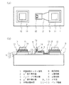
高周波用半導体装置では、その電極に接続するリード線によりインダクタンスや容量が発生し、リード線の太さや長さにより高周波特性が変化するため、できるだけその影響を受けないように、半導体装置の表面の電極上にバンプ電極を形成し、配線基板上に半導体チップを裏返しにして直接バンプ電極により回路配線と電気的に接続すると共に固定するフリップチップ型の半導体装置が用いられている。このようなフリップチップ型の高周波用半導体装置の一例として、pinダイオードの平面および断面の説明図が図6に示されている。
【0003】
図6において、半絶縁性のGaAs基板31の表面に、CVD法などによりn+ 型GaAs層32、ノンドープのGaAs層33、p+ 型GaAs層34が順次積層され、動作領域を区画する面積の周囲をn+ 型GaAs層32が露出するまでメサ状にエッチングをすると共に、さらにn+ 型GaAs層32もGaAs基板31が露出するようにメサ状にエッチングされている。そして、エッチングにより露出したn+ 型GaAs層32の表面および積層されたp+ 型GaAs層34上にそれぞれカソード電極35、アノード電極36がリフトオフ法などにより設けられている。このような不純物濃度の低いノンドープGaAs層33を挟んで形成されるpinダイオードは、逆バイアスでは容量として機能し、順バイアスでは抵抗として機能する。すなわち、電気的な特性としては、静電容量と直列抵抗として考慮する必要がある。
【0004】
そのため、pinダイオードを高周波回路において用いる場合、回路として高性能を実現するためには、前述の静電容量をできるだけ小さく、かつ、順方向の直列抵抗をできるだけ小さくする必要があり、この両者を満たしながら、ミリ波またはそれより高周波数の領域で使用するためには、pinダイオードの接合面積を10〜20μm角程度に抑える必要がある。このような理由により、前述のアノード電極36は非常に面積が小さく、この表面およびカソード電極35上に直接バンプ電極を形成して、配線基板などに直接熱圧着などにより接続しようとすると、圧力集中によるメサ部の破損や素子全体の接着強度不足が生じる。そのため、図6に示されるように、pinダイオードの両横にさらにメサ部37、38が形成され、そのメサ部37、38まで配線40、41が絶縁膜39を介して設けられ、メサ部37、38上にバンプ電極42、43がそれぞれ形成されている。
【0005】
【発明が解決しようとする課題】
前述のように、メサ型の動作領域から離れた部分にさらにメサ部37、38を形成し、そのメサ部37、38にバンプ電極42、43を形成し、そのバンプ電極42、43と素子の電極35、36とを配線40、41により接続する構造をとると、たとえば図6に示される例では、アノード電極36とバンプ電極43とを結ぶ配線41が、素子部のn+ 型GaAs層32の側壁を絶縁膜39を介して通るため、その部分(A部)で不要な寄生容量が発生し、高周波特性を悪化させるという問題がある。
【0006】
一方、このような問題を避けるためには、アノード電極36とバンプ電極43との接続をメタル配線41によらないで、ワイヤなどによるエアブリッジ配線で行うことも考えられる。しかし、エアブリッジ配線を行うと製造工程が複雑になりコストアップになると共に、構造的に信頼性が低下する。さらに、配線が細くなり、インダクタンスの発生などの問題も生じる。
【0007】
本発明は、このような問題を解決するためになされたもので、余計な配線をしないで、素子の狭い領域の電極上に直接バンプ電極を形成しながら、配線基板などに熱圧着によりマウントする際には圧力が狭い活性領域に集中して活性領域を破損したり、接着強度不足が起こらないような構造の高周波用の半導体装置を提供することを目的とする。
【0008】
【課題を解決するための手段】
本発明の高周波回路装置は、半絶縁性の基板の一表面にマイクロ波回路を構成するマイクロストリップ線路が形成され、前記基板の裏面に接地電極が設けられ、前記マイクロストリップ線路の端部間に半導体装置がボンディングされてなる高周波回路装置において、前記半導体装置は、基板上に少なくとも第1導電型半導体層および第2導電型半導体層を含む半導体層が積層される半導体積層部と、該半導体積層部が下層の第1導電型半導体層が露出するようにメサ型にエッチングされることにより形成される動作領域と、前記露出する第1導電型半導体層上に設けられる第1の電極と、前記動作領域の上層の第2導電型の半導体層上に設けられる第2の電極と、前記動作領域の横側に設けられる前記半導体積層部からなる少なくとも2つのメサ部と、該少なくとも2つのメサ部の1つに前記第1の電極と電気的に接続して設けられる第1のバンプ電極と、前記第2の電極上に設けられる第2のバンプ電極と、前記メサ部の残りの表面にスペーサ用として設けられる第3のバンプ電極とからなり、前記接地電極は前記半絶縁性の基板に設けられるスルーホールを介して前記半絶縁性の基板の表面に設けられた表面接地電極と電気的に接続され、該表面接地電極と前記マイクロストリップ線路との間に前記半導体装置の第1および第2の電極が前記第1および第2のバンプ電極を介してそれぞれ接続され、かつ、該半導体装置の第3のバンプ電極が前記マイクロストリップ線路またはマイクロストリップ線路と電気的に絶縁された導体上にボンディングされてなることを特徴とする。
【0013】
【発明の実施の形態】
つぎに、図面を参照しながら本発明の半導体装置およびそれを用いた高周波回路装置について説明をする。
【0014】
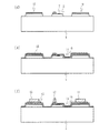
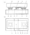
本発明による半導体装置は、図1にその一実施形態である高周波用のpinダイオードの平面および断面の説明図が示されるように、基板1上に少なくとも第1導電型(たとえばn型)の半導体層2および第2導電型(たとえばp型)の半導体層4を含む半導体層が積層されて半導体積層部5が形成されている。そして、その半導体積層部5が下層の第1導電型(n+ 型)半導体層2が露出するようにメサ型にエッチングされることにより、高周波用の動作領域6が形成されている。そして、露出するn+ 型半導体層2上に第1の電極(n側電極)7が、動作領域6の上層の第2導電型(p+ 型)の半導体層4上に第2の電極(p側電極)8がそれぞれ設けられている。さらに、動作領域6の横側に、半導体積層部5からなる少なくとも2つのメサ部9、10が設けられている。この少なくとも2つのうちの1つのメサ部9にn側電極7と電気的に接続して、第1のバンプ電極11が設けられ、p側電極8上に第2のバンプ電極12が、さらに、前記少なくとも2つのメサ部の残りのメサ部10の表面にn側およびp側の電極7、8と電気的に独立して、第3のバンプ電極13がそれぞれ設けられている。
【0015】
前記2つのメサ部は、動作領域6が中心部に位置するように設けられることが安定性の点から好ましい。ここに動作領域6が中心部に位置するとは、動作領域以外のメサ部が2つの場合はその2つのメサ部を結ぶ線上に該動作領域が位置するように、また、動作領域以外のメサ部が3個以上あるときは、3個以上ののメサ部により形成される円の中心部近傍に該動作領域が位置するようにそれぞれのメサ部が形成されることを意味する。
【0016】
図1に示される例は、高周波用のpinダイオードの例で、基板1として、半絶縁性のGaAs基板が用いられている。そして、その上にn+ 型GaAs層2、ノンドープのGaAs層3およびp+ 型GaAs層4が順次エピタキシャル成長されることにより、半導体積層部5が形成され、pinダイオードが構成されている。このpinダイオードの動作領域6は、その面積が大きすぎると逆バイアス時の接合容量が大きくなり、面積が小さすぎると順方向の直列抵抗が大きくなるため、ミリ波以上の高周波用のpinダイオードでは、前述のように10〜20μm角程度の大きさになるようにメサ状にエッチングされて、n+ 型GaAs層2が露出している。このn+ 型GaAs層2の露出は、第1の電極(n側電極)7を形成するためで、たとえば100μm角程度の大きさになるようにエッチングされてその周囲は半絶縁性GaAs基板1が露出している。
【0017】
この動作領域6(pinダイオード部)のメサ形状のエッチングと同時に前述の半導体積層部5をエッチングすることにより、たとえば動作領域6に関して対称方向になるように2つのメサ部9、10が同様に絶縁性GaAs基板1が露出するように形成されている。そして、そのメサ部9、10上、およびp側電極8上に、電極メタル14および配線メタル15を介して、バンプ電極11、13および12が、それぞれ形成されている。メサ部9上の電極メタル14およびメタル配線15はそれぞれn側電極7と接続されるように形成されており、バンプ電極11はn側電極7と電気的に接続されている。しかし、メサ部10上の電極メタル14およびメタル配線15は共にどことも接続されておらず、バンプ電極13も独立して設けられており、単にスペーサ用として設けられている。
【0018】
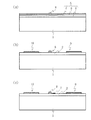
このpinダイオードの製造方法を図2〜3の工程説明図を参照しながら詳細に説明する。
【0019】
まず、図2(a)に示されるように、半絶縁性GaAs基板1の表面にCVD法によりn+ 型GaAs層2、ノンドープのGaAs層3およびp+ 型GaAs層4を順次エピタキシャル成長し、半導体積層部5を形成する。そして、動作領域6とする部分の表面にリフトオフ法により、Ti/Pt/Auなどの金属を真空蒸着することにより、20μm角程度の大きさのp側電極8を形成する。
【0020】
つぎに、表面の全面にホトレジスト膜を設け、動作領域6部が20μm角程度の大きさで被覆され、他の部分が開口されるようにパターニングをし、n+ 型GaAs層2が露出するように半導体積層部5をリン酸と過酸化水素水との混合液によりエッチングし、図2(b)に示されるようなメサ形状にする。この際に、図2(b)に示されるように、メサ部9、10が動作領域6の両横に形成されるようにレジスト膜をパターニングする。
【0021】
その後、図2(c)に示されるように、n側電極7を、露出したn+ 型GaAs層2上に前述のp側電極8と同様にリフトオフ法により形成する。
【0022】
その後、図3(d)に示されるように、n側電極7の周囲のn+ 型GaAs層2をエッチングし、半絶縁性GaAs基板1を露出させて、完全なメサ形状にする。このGaAs層2のエッチングは、前述の半導体積層部5のエッチングと同様に、全面にホトレジスト膜を設け、エッチングする部分を開口し、同様のエッチング液によりエッチングをすることにより行える。この際、前述のメサ部9、10も半絶縁性基板1が露出するメサ部になるように形成される。
【0023】
ついで、図3(e)に示されるように、電解メッキをするための、たとえば Ti/Pt/Auからなる電極メタル14を全面に真空蒸着などにより、たとえば0.5μm程度の厚さに設ける。そして、全面にホトレジスト膜を設け、メタル配線15を設ける部分を開口してAuを電解メッキすることにより、メタル配線15を、たとえば3μm程度の厚さに形成する。
【0024】
そして、さらにレジスト膜を設けて、バンプ電極11、12、13を設ける部分を開口して、Auを電解メッキすることにより、図3(f)に示されるように、第1および第3のバンプ電極11、13を、たとえば100μm角程度で20μm程度の厚さに、第2のバンプ電極12を、たとえば20μm角程度で20μm程度の厚さにそれぞれ形成する。
【0025】
その後、メタル配線15およびバンプ電極11〜13をマスクとして、反応性イオンエッチングにより、露出する電極メタル14をエッチングして除去することにより、図1に示されるようなバンプ電極11〜13が形成された高周波用のフリップチップ型のpinダイオードが形成される。
【0026】
本発明の半導体装置によれば、高周波用で動作領域が非常に小さい面積の半導体層に直接バンプ電極を設けながら、その両横、または周囲にそれより面積の大きなバンプ電極が設けられており、半導体装置をマウントする際の圧力は周囲の大きなバンプ電極により支えられ、狭い動作領域に大きな力が加わることはない。その結果、狭い動作領域に大きな力が加わって、動作領域の半導体積層部を破損したり、歪みによる特性の変化などは生じない。一方、狭い動作領域の電極に直接バンプ電極が設けられることにより、配線基板などに半導体装置をマウントする際に、その電極を直接電気的にストリップ配線などと接続することができ、半導体装置上を配線により引き出して広い領域に電極を形成する必要がなくなるため、配線による寄生容量やインダクタンスなど特性への影響をなくすることができる。
【0027】
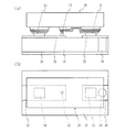
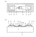
前述の半導体装置20をストリップライン22、23が形成されたセラミック基板21にマウントされた状態の断面および平面の説明図が図4に示されている。すなわち、図4に示されるように、セラミック基板21のストリップライン22、23上に半導体装置20を裏向き(upside down)にして、第1および第2のバンプ電極11、12が重なるように位置合せをして、セラミック基板21の基板温度を380℃程度にし、加重300gを印加し、60秒程度熱圧着することによりボンディングされた状態が示されている。図4の例では、セラミック基板1の裏面に接地電極25が設けられ、スルーホール24を介して一方のストリップライン23が接地電極25と電気的に接続されて表面接地電極とされている。
【0028】
この例では、第3のバンプ電極13もストリップライン22上に熱圧着されるているが、第3のバンプ電極13は電気的にフロートの状態であるため、何ら支障はない。しかし、この第3のバンプ電極13は、たとえば図5に他の例の同様の図が示されるように、ストリップラインとは電気的に絶縁して設けられた導体膜26上に熱圧着されるようにすれば、寄生インダクタンスや容量をさらに低減できるので好ましい。なお、図5において、図4と同じ部分には同じ符号を付してその説明を省略する。このように、小さなバンプ電極12部が大きなバンプ電極11、13の間にあるため、熱圧着の際の圧力が集中することがなく、小さな面積の動作領域に力が加わって破損したり、半導体積層部に歪みなどが入ることはない。
【0029】
前述の例では、pinダイオードの例であったが、pinダイオードに限らず、pn接合ダイオードやトランジスタなどでも、所定の電極に直接バンプ電極を形成して、半導体装置の表面に配線を引き回すことなく接続しながら、小さなバンプ電極に熱圧着の際の力が集中しないように、電極に接続されないダミー電極が同様に設けられることにより、基板などへのマウントの際に、狭い領域への力の集中を避けることができ、優れた半導体特性を得ることができる。
【0030】
【発明の効果】
本発明によれば、小さなメサ電極部に直接バンプ電極を設けながら、電極には接続されないダミーのバンプ電極により保護されるため、回路基板などに熱圧着する際の破損などもなく、寄生容量などの発生もないため、高周波数に対しても、高特性の半導体装置が得られ、信頼性も非常に向上する。
【0031】
さらに、本発明によれば、従来と同様の製造工程で製造することができると共に、従来バンプ電極を別の場所に設けるためのメタル配線を形成するため、その下に絶縁膜を設けなければならなかったものが必要でなくなり、絶縁膜を設ける工数を削減することができる。
【図面の簡単な説明】
【図1】本発明の半導体装置の一実施形態であるフリップチップ型メサ構造のpinダイオードの平面および断面の説明図である。
【図2】図1の半導体装置の製造方法の一例の製造工程を示す断面説明図である。
【図3】図1の半導体装置の製造方法の一例の製造工程を示す断面説明図である。
【図4】図1の半導体装置をストリップラインが形成された基板にマウントした状態の断面および平面の説明図である。
【図5】図1の半導体装置をストリップラインが形成された基板にマウントした状態の他の例の断面および平面の説明図である。
【図6】従来のフリップチップ型のメサ構造のpinダイオードの平面および断面の説明図である。
【符号の説明】
1 半絶縁性GaAs基板
2 n+ 型半導体層
3 ノンドープ半導体層
4 p+ 型半導体層
5 半導体積層部
6 動作領域
7 n側電極
8 p側電極
9、10 メサ部
11〜13 バンプ電極[0001]
BACKGROUND OF THE INVENTION
The present invention relates to a semiconductor device used in a higher frequency region than millimeter waves and millimeter waves. More specifically, the present invention relates to a flip-chip type semiconductor device that can be directly connected to a wiring board on which a microstrip line or the like is formed without using a wire.
[0002]
[Prior art]
In a high-frequency semiconductor device, inductance and capacitance are generated by the lead wire connected to the electrode, and the high-frequency characteristics change depending on the thickness and length of the lead wire, so that the surface of the semiconductor device is not affected as much as possible. 2. Description of the Related Art Flip chip type semiconductor devices are used in which bump electrodes are formed on electrodes, a semiconductor chip is turned over on a wiring board, and directly connected and fixed to circuit wiring by bump electrodes. As an example of such a flip-chip type high-frequency semiconductor device, a plane and cross-sectional explanatory view of a pin diode is shown in FIG.
[0003]
In FIG. 6, an n.sup. +
[0004]
Therefore, when a pin diode is used in a high-frequency circuit, in order to realize high performance as a circuit, it is necessary to reduce the aforementioned capacitance as much as possible and the forward series resistance as much as possible. However, in order to use in the millimeter wave or higher frequency region, it is necessary to suppress the junction area of the pin diode to about 10 to 20 μm square. For this reason, the above-mentioned
[0005]
[Problems to be solved by the invention]
As described above,
[0006]
On the other hand, in order to avoid such a problem, it is conceivable that the
[0007]
The present invention has been made to solve such a problem, and is mounted on a wiring board or the like by thermocompression bonding while forming a bump electrode directly on an electrode in a narrow region of the element without extra wiring. It is an object of the present invention to provide a high-frequency semiconductor device having a structure in which the active region is not concentrated due to a narrow pressure, and the active region is not damaged or the adhesive strength is not insufficient.
[0008]
[Means for Solving the Problems]
In the high-frequency circuit device of the present invention, a microstrip line constituting a microwave circuit is formed on one surface of a semi-insulating substrate, a ground electrode is provided on the back surface of the substrate, and between the ends of the microstrip line. In a high-frequency circuit device formed by bonding a semiconductor device, the semiconductor device includes a semiconductor stacked portion in which a semiconductor layer including at least a first conductive semiconductor layer and a second conductive semiconductor layer is stacked on a substrate, and the semiconductor stacked layer An operation region formed by etching into a mesa shape so that the first conductive type semiconductor layer of the lower layer is exposed; a first electrode provided on the exposed first conductive type semiconductor layer; At least two layers including a second electrode provided on the second conductivity type semiconductor layer in the upper layer of the operation region and the semiconductor stacked portion provided on the lateral side of the operation region. A first bump electrode provided on one of the at least two mesa portions and electrically connected to the first electrode; a second bump electrode provided on the second electrode; , and a third bump electrode provided as a spacer on the remaining surface of the mesa portion, the ground electrode of the substrate of the semi-insulating through the through hole provided in a substrate of the semi-insulating The first and second electrodes of the semiconductor device are electrically connected to a surface ground electrode provided on the surface, and the first and second bump electrodes are connected between the surface ground electrode and the microstrip line. And a third bump electrode of the semiconductor device is bonded onto the microstrip line or a conductor electrically insulated from the microstrip line.
[0013]
DETAILED DESCRIPTION OF THE INVENTION
Next, a semiconductor device of the present invention and a high-frequency circuit device using the same will be described with reference to the drawings.
[0014]
The semiconductor device according to the present invention is a semiconductor of at least a first conductivity type (for example, n-type) on a
[0015]
It is preferable from the viewpoint of stability that the two mesa portions are provided so that the
[0016]
The example shown in FIG. 1 is an example of a high-frequency pin diode, and a semi-insulating GaAs substrate is used as the
[0017]
By simultaneously etching the semiconductor laminated
[0018]
A manufacturing method of this pin diode will be described in detail with reference to the process explanatory diagrams of FIGS.
[0019]
First, as shown in FIG. 2A, an n.sup. +
[0020]
Next, a photoresist film is provided on the entire surface, and patterning is performed so that 6 parts of the operation region are covered with a size of about 20 μm square and the other part is opened, so that the n + -
[0021]
Thereafter, as shown in FIG. 2C, the n-
[0022]
Thereafter, as shown in FIG. 3D, the n + -
[0023]
Next, as shown in FIG. 3E, an
[0024]
Then, a resist film is further provided, the portions where the
[0025]
Thereafter, by using the
[0026]
According to the semiconductor device of the present invention, a bump electrode having a larger area is provided on both sides or the periphery of the semiconductor layer while providing the bump electrode directly on a semiconductor layer having a very small area for high frequency operation. The pressure at the time of mounting the semiconductor device is supported by a large surrounding bump electrode, and a large force is not applied to a narrow operation region. As a result, a large force is applied to the narrow operation region, and the semiconductor stacked portion in the operation region is not damaged, and the characteristics are not changed by the distortion. On the other hand, since the bump electrode is directly provided on the electrode in the narrow operation region, when mounting the semiconductor device on the wiring board or the like, the electrode can be directly and electrically connected to the strip wiring or the like. Since it is not necessary to form electrodes in a wide area by drawing out by wiring, it is possible to eliminate the influence on characteristics such as parasitic capacitance and inductance due to wiring.
[0027]
FIG. 4 shows an explanatory view of a cross section and a plan view of the
[0028]
In this example, the
[0029]
In the above example, the pin diode is used. However, not only the pin diode but also a pn junction diode, a transistor, or the like, a bump electrode is directly formed on a predetermined electrode, and a wiring is not drawn around the surface of the semiconductor device. A dummy electrode that is not connected to the electrode is provided in the same way so that the force at the time of thermocompression bonding does not concentrate on the small bump electrode while connecting, so that the force is concentrated on a narrow area when mounting on a substrate etc. Can be avoided, and excellent semiconductor characteristics can be obtained.
[0030]
【The invention's effect】
According to the present invention, a bump electrode is provided directly on a small mesa electrode portion, and is protected by a dummy bump electrode that is not connected to the electrode. Therefore, a high-performance semiconductor device can be obtained even at high frequencies, and the reliability is greatly improved.
[0031]
Furthermore, according to the present invention, it is possible to manufacture in the same manufacturing process as in the prior art, and in order to form the metal wiring for providing the bump electrode in another place, an insulating film must be provided thereunder. What was not needed is no longer necessary, and the number of steps for providing the insulating film can be reduced.
[Brief description of the drawings]
BRIEF DESCRIPTION OF DRAWINGS FIG. 1 is an explanatory view of a plane and a cross section of a flip-chip mesa pin diode that is an embodiment of a semiconductor device of the present invention.
2 is a cross-sectional explanatory view showing the manufacturing process of the example of the manufacturing method of the semiconductor device of FIG. 1; FIG.
3 is a cross-sectional explanatory view showing the manufacturing process of the example of the manufacturing method of the semiconductor device of FIG. 1; FIG.
4 is an explanatory view of a cross section and a plan view of a state in which the semiconductor device of FIG. 1 is mounted on a substrate on which a strip line is formed.
5 is an explanatory view of a cross section and a plan view of another example in which the semiconductor device of FIG. 1 is mounted on a substrate on which a strip line is formed. FIG.
FIG. 6 is an explanatory view of a plane and a cross section of a conventional flip chip type mesa structure pin diode.
[Explanation of symbols]
DESCRIPTION OF
Claims (1)
Priority Applications (1)
| Application Number | Priority Date | Filing Date | Title |
|---|---|---|---|
| JP15452499A JP3913402B2 (en) | 1999-06-02 | 1999-06-02 | High frequency circuit equipment |
Applications Claiming Priority (1)
| Application Number | Priority Date | Filing Date | Title |
|---|---|---|---|
| JP15452499A JP3913402B2 (en) | 1999-06-02 | 1999-06-02 | High frequency circuit equipment |
Publications (2)
| Publication Number | Publication Date |
|---|---|
| JP2000349113A JP2000349113A (en) | 2000-12-15 |
| JP3913402B2 true JP3913402B2 (en) | 2007-05-09 |
Family
ID=15586152
Family Applications (1)
| Application Number | Title | Priority Date | Filing Date |
|---|---|---|---|
| JP15452499A Expired - Lifetime JP3913402B2 (en) | 1999-06-02 | 1999-06-02 | High frequency circuit equipment |
Country Status (1)
| Country | Link |
|---|---|
| JP (1) | JP3913402B2 (en) |
Families Citing this family (11)
| Publication number | Priority date | Publication date | Assignee | Title |
|---|---|---|---|---|
| US6348739B1 (en) * | 1999-04-28 | 2002-02-19 | Matsushita Electric Industrial Co., Ltd. | Semiconductor device and method of manufacturing the same |
| JP2005129776A (en) * | 2003-10-24 | 2005-05-19 | Hamamatsu Photonics Kk | Semiconductor light receiving element |
| JP4279650B2 (en) * | 2003-10-24 | 2009-06-17 | 浜松ホトニクス株式会社 | Semiconductor photo detector |
| CN101341600B (en) * | 2005-12-26 | 2012-11-28 | 日本电气株式会社 | Semiconductor optical device |
| CN100485971C (en) * | 2006-09-06 | 2009-05-06 | 中国科学院微电子研究所 | Gallium arsenide PIN diode and manufacturing method thereof |
| JP5300375B2 (en) * | 2008-08-26 | 2013-09-25 | 日本オクラロ株式会社 | Back-illuminated light receiving element and manufacturing method thereof |
| JP2010267647A (en) * | 2009-05-12 | 2010-11-25 | Opnext Japan Inc | Semiconductor device |
| JP5483544B2 (en) * | 2009-10-21 | 2014-05-07 | 住友電工デバイス・イノベーション株式会社 | Semiconductor photo detector |
| JP5642593B2 (en) * | 2010-05-18 | 2014-12-17 | 日本オクラロ株式会社 | Back-illuminated semiconductor photo detector, optical receiver module, optical transceiver |
| GB2593864B (en) | 2020-02-28 | 2023-01-04 | X Fab France Sas | Improved transfer printing for RF applications |
| US12476194B2 (en) * | 2021-01-06 | 2025-11-18 | Mediatek Singapore Pte. Ltd. | Semiconductor structure |
-
1999
- 1999-06-02 JP JP15452499A patent/JP3913402B2/en not_active Expired - Lifetime
Also Published As
| Publication number | Publication date |
|---|---|
| JP2000349113A (en) | 2000-12-15 |
Similar Documents
| Publication | Publication Date | Title |
|---|---|---|
| US4339870A (en) | Series-connected two-terminal semiconductor devices and their fabrication | |
| CN100364111C (en) | Gunn diode and mounting structure thereof | |
| JP3913402B2 (en) | High frequency circuit equipment | |
| CN114373724A (en) | Semiconductor module | |
| US10475717B2 (en) | Semiconductor chip, method for mounting semiconductor chip, and module in which semiconductor chip is packaged | |
| US12136664B2 (en) | Semiconductor device and method for producing the same | |
| US10163829B2 (en) | Compound semiconductor substrate and power amplifier module | |
| CN102376664B (en) | Semiconductor device, semiconductor circuit substrate, and method of manufacturing semiconductor circuit substrate | |
| JP3946360B2 (en) | Gunn diode, manufacturing method thereof, and mounting structure thereof | |
| US4127830A (en) | Microstrip switch wherein diodes are formed in single semiconductor body | |
| CN114142340A (en) | Surface Emitting Semiconductor Laser | |
| JPS61111574A (en) | Monolithic semiconductor structure and making thereof | |
| JP2006114732A (en) | Semiconductor device, manufacturing method thereof, and semiconductor module | |
| JP2000068714A (en) | Millimeter-wave matching circuit and communication module | |
| JP7332130B2 (en) | Semiconductor device manufacturing method, semiconductor device manufacturing method, semiconductor device, and semiconductor device | |
| WO2023124249A1 (en) | Hybrid monolithic microwave integrated circuit and manufacturing method therefor | |
| JP2000101067A (en) | Semiconductor device and integrated circuit device | |
| US12262556B2 (en) | Power amplifier | |
| JP3631428B2 (en) | Semiconductor device having flip-chip mounting structure | |
| JP3766621B2 (en) | Package for housing input/output terminals and semiconductor elements | |
| JP2000114423A (en) | Semiconductor element mounting method | |
| JPH10144801A (en) | Semiconductor device | |
| JP4516287B2 (en) | Surface mount gun diode and mounting method thereof | |
| JP2004103819A (en) | Monolithic microwave integrated circuit | |
| JPH0669072B2 (en) | Method for manufacturing semiconductor device |
Legal Events
| Date | Code | Title | Description |
|---|---|---|---|
| A621 | Written request for application examination |
Free format text: JAPANESE INTERMEDIATE CODE: A621 Effective date: 20050407 |
|
| A977 | Report on retrieval |
Free format text: JAPANESE INTERMEDIATE CODE: A971007 Effective date: 20060731 |
|
| A131 | Notification of reasons for refusal |
Free format text: JAPANESE INTERMEDIATE CODE: A131 Effective date: 20060808 |
|
| A521 | Request for written amendment filed |
Free format text: JAPANESE INTERMEDIATE CODE: A523 Effective date: 20061003 |
|
| A131 | Notification of reasons for refusal |
Free format text: JAPANESE INTERMEDIATE CODE: A131 Effective date: 20061031 |
|
| A521 | Request for written amendment filed |
Free format text: JAPANESE INTERMEDIATE CODE: A523 Effective date: 20061225 |
|
| TRDD | Decision of grant or rejection written | ||
| A01 | Written decision to grant a patent or to grant a registration (utility model) |
Free format text: JAPANESE INTERMEDIATE CODE: A01 Effective date: 20070123 |
|
| A61 | First payment of annual fees (during grant procedure) |
Free format text: JAPANESE INTERMEDIATE CODE: A61 Effective date: 20070131 |
|
| R150 | Certificate of patent or registration of utility model |
Free format text: JAPANESE INTERMEDIATE CODE: R150 Ref document number: 3913402 Country of ref document: JP Free format text: JAPANESE INTERMEDIATE CODE: R150 |
|
| FPAY | Renewal fee payment (event date is renewal date of database) |
Free format text: PAYMENT UNTIL: 20130209 Year of fee payment: 6 |
|
| R250 | Receipt of annual fees |
Free format text: JAPANESE INTERMEDIATE CODE: R250 |
|
| FPAY | Renewal fee payment (event date is renewal date of database) |
Free format text: PAYMENT UNTIL: 20150209 Year of fee payment: 8 |
|
| R250 | Receipt of annual fees |
Free format text: JAPANESE INTERMEDIATE CODE: R250 |
|
| R250 | Receipt of annual fees |
Free format text: JAPANESE INTERMEDIATE CODE: R250 |
|
| R250 | Receipt of annual fees |
Free format text: JAPANESE INTERMEDIATE CODE: R250 |
|
| R250 | Receipt of annual fees |
Free format text: JAPANESE INTERMEDIATE CODE: R250 |
|
| R250 | Receipt of annual fees |
Free format text: JAPANESE INTERMEDIATE CODE: R250 |
|
| R250 | Receipt of annual fees |
Free format text: JAPANESE INTERMEDIATE CODE: R250 |
|
| EXPY | Cancellation because of completion of term |