JP3909500B2 - 光学素子および光学素子の製造方法 - Google Patents
光学素子および光学素子の製造方法 Download PDFInfo
- Publication number
- JP3909500B2 JP3909500B2 JP21290297A JP21290297A JP3909500B2 JP 3909500 B2 JP3909500 B2 JP 3909500B2 JP 21290297 A JP21290297 A JP 21290297A JP 21290297 A JP21290297 A JP 21290297A JP 3909500 B2 JP3909500 B2 JP 3909500B2
- Authority
- JP
- Japan
- Prior art keywords
- cavity
- photonics
- substrate
- spherical lens
- pyramidal
- Prior art date
- Legal status (The legal status is an assumption and is not a legal conclusion. Google has not performed a legal analysis and makes no representation as to the accuracy of the status listed.)
- Expired - Fee Related
Links
- 230000003287 optical effect Effects 0.000 title claims description 62
- 238000004519 manufacturing process Methods 0.000 title description 9
- 239000000758 substrate Substances 0.000 claims description 43
- 239000013078 crystal Substances 0.000 claims description 26
- 239000004065 semiconductor Substances 0.000 claims description 11
- 230000000903 blocking effect Effects 0.000 claims description 7
- 229910021419 crystalline silicon Inorganic materials 0.000 claims description 5
- 239000002210 silicon-based material Substances 0.000 claims description 4
- 238000005530 etching Methods 0.000 description 30
- 238000000034 method Methods 0.000 description 26
- 229910052751 metal Inorganic materials 0.000 description 14
- 239000002184 metal Substances 0.000 description 14
- XUIMIQQOPSSXEZ-UHFFFAOYSA-N Silicon Chemical compound [Si] XUIMIQQOPSSXEZ-UHFFFAOYSA-N 0.000 description 13
- 229910052710 silicon Inorganic materials 0.000 description 13
- 239000010703 silicon Substances 0.000 description 13
- 239000013307 optical fiber Substances 0.000 description 12
- KWYUFKZDYYNOTN-UHFFFAOYSA-M Potassium hydroxide Chemical compound [OH-].[K+] KWYUFKZDYYNOTN-UHFFFAOYSA-M 0.000 description 10
- 230000008569 process Effects 0.000 description 9
- 238000010586 diagram Methods 0.000 description 6
- 230000008878 coupling Effects 0.000 description 5
- 238000010168 coupling process Methods 0.000 description 5
- 238000005859 coupling reaction Methods 0.000 description 5
- 230000000873 masking effect Effects 0.000 description 5
- 230000005540 biological transmission Effects 0.000 description 4
- 239000004593 Epoxy Substances 0.000 description 3
- 238000004891 communication Methods 0.000 description 3
- 238000001514 detection method Methods 0.000 description 3
- 238000000206 photolithography Methods 0.000 description 3
- 238000013461 design Methods 0.000 description 2
- 230000004044 response Effects 0.000 description 2
- 229910000679 solder Inorganic materials 0.000 description 2
- 239000000853 adhesive Substances 0.000 description 1
- 230000001070 adhesive effect Effects 0.000 description 1
- 229910052782 aluminium Inorganic materials 0.000 description 1
- XAGFODPZIPBFFR-UHFFFAOYSA-N aluminium Chemical compound [Al] XAGFODPZIPBFFR-UHFFFAOYSA-N 0.000 description 1
- 230000008859 change Effects 0.000 description 1
- 230000001427 coherent effect Effects 0.000 description 1
- 239000004020 conductor Substances 0.000 description 1
- 239000003292 glue Substances 0.000 description 1
- PCHJSUWPFVWCPO-UHFFFAOYSA-N gold Chemical compound [Au] PCHJSUWPFVWCPO-UHFFFAOYSA-N 0.000 description 1
- 229910052737 gold Inorganic materials 0.000 description 1
- 239000010931 gold Substances 0.000 description 1
- 238000012423 maintenance Methods 0.000 description 1
- 239000000463 material Substances 0.000 description 1
- 230000007246 mechanism Effects 0.000 description 1
- 238000001465 metallisation Methods 0.000 description 1
- 238000012986 modification Methods 0.000 description 1
- 230000004048 modification Effects 0.000 description 1
- 238000002360 preparation method Methods 0.000 description 1
- 238000012545 processing Methods 0.000 description 1
- 230000005855 radiation Effects 0.000 description 1
- 238000003466 welding Methods 0.000 description 1
Images


Classifications
-
- G—PHYSICS
- G02—OPTICS
- G02B—OPTICAL ELEMENTS, SYSTEMS OR APPARATUS
- G02B6/00—Light guides; Structural details of arrangements comprising light guides and other optical elements, e.g. couplings
- G02B6/24—Coupling light guides
- G02B6/42—Coupling light guides with opto-electronic elements
- G02B6/4201—Packages, e.g. shape, construction, internal or external details
- G02B6/4219—Mechanical fixtures for holding or positioning the elements relative to each other in the couplings; Alignment methods for the elements, e.g. measuring or observing methods especially used therefor
- G02B6/4228—Passive alignment, i.e. without a detection of the degree of coupling or the position of the elements
- G02B6/423—Passive alignment, i.e. without a detection of the degree of coupling or the position of the elements using guiding surfaces for the alignment
-
- G—PHYSICS
- G02—OPTICS
- G02B—OPTICAL ELEMENTS, SYSTEMS OR APPARATUS
- G02B6/00—Light guides; Structural details of arrangements comprising light guides and other optical elements, e.g. couplings
- G02B6/24—Coupling light guides
- G02B6/42—Coupling light guides with opto-electronic elements
- G02B6/4201—Packages, e.g. shape, construction, internal or external details
- G02B6/4219—Mechanical fixtures for holding or positioning the elements relative to each other in the couplings; Alignment methods for the elements, e.g. measuring or observing methods especially used therefor
- G02B6/4233—Active alignment along the optical axis and passive alignment perpendicular to the optical axis
-
- G—PHYSICS
- G02—OPTICS
- G02B—OPTICAL ELEMENTS, SYSTEMS OR APPARATUS
- G02B6/00—Light guides; Structural details of arrangements comprising light guides and other optical elements, e.g. couplings
- G02B6/24—Coupling light guides
- G02B6/42—Coupling light guides with opto-electronic elements
- G02B6/4201—Packages, e.g. shape, construction, internal or external details
- G02B6/4219—Mechanical fixtures for holding or positioning the elements relative to each other in the couplings; Alignment methods for the elements, e.g. measuring or observing methods especially used therefor
- G02B6/4236—Fixing or mounting methods of the aligned elements
- G02B6/4238—Soldering
-
- G—PHYSICS
- G02—OPTICS
- G02B—OPTICAL ELEMENTS, SYSTEMS OR APPARATUS
- G02B6/00—Light guides; Structural details of arrangements comprising light guides and other optical elements, e.g. couplings
- G02B6/24—Coupling light guides
- G02B6/42—Coupling light guides with opto-electronic elements
- G02B6/4201—Packages, e.g. shape, construction, internal or external details
- G02B6/4219—Mechanical fixtures for holding or positioning the elements relative to each other in the couplings; Alignment methods for the elements, e.g. measuring or observing methods especially used therefor
- G02B6/4236—Fixing or mounting methods of the aligned elements
- G02B6/4239—Adhesive bonding; Encapsulation with polymer material
Landscapes
- Physics & Mathematics (AREA)
- General Physics & Mathematics (AREA)
- Optics & Photonics (AREA)
- Optical Couplings Of Light Guides (AREA)
- Light Receiving Elements (AREA)
Applications Claiming Priority (2)
| Application Number | Priority Date | Filing Date | Title |
|---|---|---|---|
| US705,867 | 1991-05-28 | ||
| US08/705,867 US5771323A (en) | 1996-08-28 | 1996-08-28 | Micro-photonics module |
Publications (3)
| Publication Number | Publication Date |
|---|---|
| JPH1082932A JPH1082932A (ja) | 1998-03-31 |
| JPH1082932A5 JPH1082932A5 (enExample) | 2005-04-07 |
| JP3909500B2 true JP3909500B2 (ja) | 2007-04-25 |
Family
ID=24835282
Family Applications (1)
| Application Number | Title | Priority Date | Filing Date |
|---|---|---|---|
| JP21290297A Expired - Fee Related JP3909500B2 (ja) | 1996-08-28 | 1997-08-07 | 光学素子および光学素子の製造方法 |
Country Status (4)
| Country | Link |
|---|---|
| US (1) | US5771323A (enExample) |
| EP (1) | EP0826993B1 (enExample) |
| JP (1) | JP3909500B2 (enExample) |
| DE (1) | DE69727343T2 (enExample) |
Families Citing this family (14)
| Publication number | Priority date | Publication date | Assignee | Title |
|---|---|---|---|---|
| US5911021A (en) * | 1997-04-02 | 1999-06-08 | Lucent Technologies Inc. | Subassembly and method for coupling optical devices |
| KR100553877B1 (ko) * | 1999-04-29 | 2006-02-24 | 삼성전자주식회사 | 광소자모듈 |
| US6907054B2 (en) * | 2001-06-29 | 2005-06-14 | Sharp Kabushiki Kaisha | Semiconductor laser device |
| US6728449B2 (en) | 2002-02-14 | 2004-04-27 | Agilent Technologies, Inc. | Fiber assembly alignment using fiducials |
| US20030219211A1 (en) * | 2002-05-22 | 2003-11-27 | Yu-Sik Kim | Method for aligning optical axis of an optical module |
| US6888988B2 (en) * | 2003-03-14 | 2005-05-03 | Agilent Technologies, Inc. | Small form factor all-polymer optical device with integrated dual beam path based on total internal reflection optical turn |
| US7688689B2 (en) * | 2004-02-26 | 2010-03-30 | Seagate Technology Llc | Head with optical bench for use in data storage devices |
| US7128476B1 (en) * | 2004-08-20 | 2006-10-31 | The United States Of America As Represented By The National Security Agency | Photonic integrated circuit and method of fabricating same |
| US8050526B2 (en) * | 2005-02-08 | 2011-11-01 | Samsung Electronics Co., Ltd. | Micro-optical device and method of making same |
| EP3935763A4 (en) | 2019-03-06 | 2022-12-07 | Lightmatter, Inc. | Photonic communication platform |
| KR20220137062A (ko) * | 2020-02-03 | 2022-10-11 | 라이트매터, 인크. | 광자 웨이퍼 통신 시스템들 및 관련 패키지들 |
| CN118202286A (zh) | 2021-10-13 | 2024-06-14 | 光物质公司 | 多光罩光子通信平台上的多租户隔离 |
| KR20240165455A (ko) | 2022-03-28 | 2024-11-22 | 라이트매터, 인크. | 포토닉 통신 플랫폼 및 관련된 아키텍처들, 시스템들 및 방법들 |
| US12147078B2 (en) | 2022-11-11 | 2024-11-19 | Lightmatter, Inc. | Polarization locker for fiber connections and related methods |
Family Cites Families (13)
| Publication number | Priority date | Publication date | Assignee | Title |
|---|---|---|---|---|
| JPS5938564B2 (ja) * | 1979-09-20 | 1984-09-18 | 松下電器産業株式会社 | 結合器 |
| JPS6296912A (ja) * | 1985-10-24 | 1987-05-06 | Fujitsu Ltd | 光学レンズの固定構造 |
| DE3939723C1 (en) * | 1989-12-01 | 1991-02-14 | Ant Nachrichtentechnik Gmbh, 7150 Backnang, De | Optical or opto-electronic coupling - uses spherical lens received in frusto-pyramidal recess of one part and groove of other part |
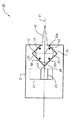
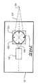
| US5124281A (en) * | 1990-08-27 | 1992-06-23 | At&T Bell Laboratories | Method of fabricating a photonics module comprising a spherical lens |
| US5181216A (en) * | 1990-08-27 | 1993-01-19 | At&T Bell Laboratories | Photonics module apparatus |
| DE4133220C2 (de) * | 1991-10-07 | 1994-12-15 | Siemens Ag | Fasern-Linsen-Anordnung zum optischen Koppeln |
| US5307434A (en) * | 1992-07-16 | 1994-04-26 | At&T Bell Laboratories | Article that comprises a laser coupled to an optical fiber |
| US5291572A (en) * | 1993-01-14 | 1994-03-01 | At&T Bell Laboratories | Article comprising compression bonded parts |
| JP3302458B2 (ja) * | 1993-08-31 | 2002-07-15 | 富士通株式会社 | 集積化光装置及び製造方法 |
| JPH0774343A (ja) * | 1993-08-31 | 1995-03-17 | Fujitsu Ltd | 集積化光装置及びその製造方法 |
| US5367589A (en) * | 1993-10-22 | 1994-11-22 | At&T Bell Laboratories | Optical fiber package |
| US5439782A (en) * | 1993-12-13 | 1995-08-08 | At&T Corp. | Methods for making microstructures |
| DE19515688C1 (de) * | 1995-04-28 | 1996-09-26 | Bosch Gmbh Robert | Optisches Sende- und Empfangsmodul |
-
1996
- 1996-08-28 US US08/705,867 patent/US5771323A/en not_active Expired - Lifetime
-
1997
- 1997-06-17 EP EP97109858A patent/EP0826993B1/en not_active Expired - Lifetime
- 1997-06-17 DE DE69727343T patent/DE69727343T2/de not_active Expired - Fee Related
- 1997-08-07 JP JP21290297A patent/JP3909500B2/ja not_active Expired - Fee Related
Also Published As
| Publication number | Publication date |
|---|---|
| DE69727343D1 (de) | 2004-03-04 |
| DE69727343T2 (de) | 2004-12-02 |
| EP0826993B1 (en) | 2004-01-28 |
| US5771323A (en) | 1998-06-23 |
| EP0826993A1 (en) | 1998-03-04 |
| JPH1082932A (ja) | 1998-03-31 |
Similar Documents
| Publication | Publication Date | Title |
|---|---|---|
| US5848211A (en) | Photonics module having its components mounted on a single mounting member | |
| EP0473339B1 (en) | A method of mounting a spherical lens on a substrate | |
| JP3909500B2 (ja) | 光学素子および光学素子の製造方法 | |
| US5675684A (en) | Optical module having semiconductor elements fixedly mounted thereon with improved accuracy | |
| US5181216A (en) | Photonics module apparatus | |
| US11378751B2 (en) | Laser patterned adapters with waveguides and etched connectors for low cost alignment of optics to chips | |
| US8442362B2 (en) | Method for manufacturing optical coupling element, optical transmission substrate, optical coupling component, coupling method, and optical interconnect system | |
| JPH07117631B2 (ja) | 自動整合光部品 | |
| KR100329208B1 (ko) | 기능소자와 그 제조방법 및 이 기능소자를 이용한 광디스크장치 | |
| JP3167650B2 (ja) | 一体化鏡を備えた光検出器及びその作成方法 | |
| JP3168297B2 (ja) | 光学素子取り付け方法 | |
| US6023546A (en) | Structure for securing optical device and fiber optics | |
| US5930429A (en) | Micro-photonics module integrated on a single substrate | |
| KR19980045943A (ko) | 하이브리드 광집적회로용 마이크로 거울, 그의 제조방법, 마이크로 거울-광검출기 어셈블리 및 광수신용 하이브리드 광집적회로 어셈블리 | |
| US6137121A (en) | Integrated semiconductor light generating and detecting device | |
| JPH05167060A (ja) | 光結合回路 | |
| JP3295327B2 (ja) | 双方向光モジュール | |
| JPH09318845A (ja) | 光伝送モジュール | |
| US20080239520A1 (en) | Optical module having the light incident surface of a lens inclined on a substrate and a method of manufacturing the same | |
| JP3040252B2 (ja) | 半導体レーザ装置 | |
| JP2000028864A (ja) | 光半導体素子の実装方法、及び光半導体装置 | |
| JPS61203692A (ja) | 半導体レ−ザ装置の製造方法 |
Legal Events
| Date | Code | Title | Description |
|---|---|---|---|
| A521 | Request for written amendment filed |
Free format text: JAPANESE INTERMEDIATE CODE: A523 Effective date: 20040507 |
|
| A621 | Written request for application examination |
Free format text: JAPANESE INTERMEDIATE CODE: A621 Effective date: 20040507 |
|
| RD03 | Notification of appointment of power of attorney |
Free format text: JAPANESE INTERMEDIATE CODE: A7423 Effective date: 20060322 |
|
| A977 | Report on retrieval |
Free format text: JAPANESE INTERMEDIATE CODE: A971007 Effective date: 20060502 |
|
| A131 | Notification of reasons for refusal |
Free format text: JAPANESE INTERMEDIATE CODE: A131 Effective date: 20060516 |
|
| A601 | Written request for extension of time |
Free format text: JAPANESE INTERMEDIATE CODE: A601 Effective date: 20060816 |
|
| A602 | Written permission of extension of time |
Free format text: JAPANESE INTERMEDIATE CODE: A602 Effective date: 20060821 |
|
| A521 | Request for written amendment filed |
Free format text: JAPANESE INTERMEDIATE CODE: A523 Effective date: 20061116 |
|
| TRDD | Decision of grant or rejection written | ||
| A01 | Written decision to grant a patent or to grant a registration (utility model) |
Free format text: JAPANESE INTERMEDIATE CODE: A01 Effective date: 20070109 |
|
| A711 | Notification of change in applicant |
Free format text: JAPANESE INTERMEDIATE CODE: A711 Effective date: 20070116 |
|
| A61 | First payment of annual fees (during grant procedure) |
Free format text: JAPANESE INTERMEDIATE CODE: A61 Effective date: 20070116 |
|
| R150 | Certificate of patent or registration of utility model |
Free format text: JAPANESE INTERMEDIATE CODE: R150 |
|
| A711 | Notification of change in applicant |
Free format text: JAPANESE INTERMEDIATE CODE: A711 Effective date: 20070320 |
|
| S111 | Request for change of ownership or part of ownership |
Free format text: JAPANESE INTERMEDIATE CODE: R313113 |
|
| R360 | Written notification for declining of transfer of rights |
Free format text: JAPANESE INTERMEDIATE CODE: R360 |
|
| R360 | Written notification for declining of transfer of rights |
Free format text: JAPANESE INTERMEDIATE CODE: R360 |
|
| R371 | Transfer withdrawn |
Free format text: JAPANESE INTERMEDIATE CODE: R371 |
|
| S111 | Request for change of ownership or part of ownership |
Free format text: JAPANESE INTERMEDIATE CODE: R313113 |
|
| FPAY | Renewal fee payment (event date is renewal date of database) |
Free format text: PAYMENT UNTIL: 20100202 Year of fee payment: 3 |
|
| R350 | Written notification of registration of transfer |
Free format text: JAPANESE INTERMEDIATE CODE: R350 |
|
| A072 | Dismissal of procedure [no reply to invitation to correct request for examination] |
Free format text: JAPANESE INTERMEDIATE CODE: A072 Effective date: 20070717 |
|
| LAPS | Cancellation because of no payment of annual fees |