JP3897893B2 - Displacement magnifying device and micro area scanning device using the same - Google Patents
Displacement magnifying device and micro area scanning device using the same Download PDFInfo
- Publication number
- JP3897893B2 JP3897893B2 JP05391098A JP5391098A JP3897893B2 JP 3897893 B2 JP3897893 B2 JP 3897893B2 JP 05391098 A JP05391098 A JP 05391098A JP 5391098 A JP5391098 A JP 5391098A JP 3897893 B2 JP3897893 B2 JP 3897893B2
- Authority
- JP
- Japan
- Prior art keywords
- fixed
- rotating pair
- displacement
- piezoelectric element
- pair
- Prior art date
- Legal status (The legal status is an assumption and is not a legal conclusion. Google has not performed a legal analysis and makes no representation as to the accuracy of the status listed.)
- Expired - Fee Related
Links
Images


Description
【0001】
【発明の属する技術分野】
本発明は、原子間力顕微鏡(AFM)や走査型近視野顕微鏡(SNOM)に代表される走査型プローブ顕微鏡(SPM)の試料走査やプローブ走査に利用される微小領域走査装置に利用する変位拡大装置及びこれを用いた微小領域走査装置に関する。
【0002】
【従来の技術】
走査型プローブ顕微鏡(SPM)は、機械的探針(以下、プローブと呼ぶ)によって試料表面を走査し、プローブと試料表面との間に働く相互作用を検出することによって、試料表面の物理量をnm(10−9m)以下のオーダーで観察する装置である。例えば、走査型プローブ顕微鏡(SPM)の一つとして代表的な原子間力顕微鏡(AFM)では、プローブと試料表面の間に働く原子間力をプローブのたわみ量変化という情報で検出し、これを利用することによって試料の表面形状を観察することができる。
【0003】
こうした装置において、試料やプローブを水平方向(以下XY方向と呼ぶ)、もしくは水平方向と高さ方向(以下Z方向と呼ぶ)に走査するために必要な機械装置が、微小領域走査装置である。
【0004】
走査型プローブ顕微鏡(SPM)に利用される微小領域走査装置には、0.01〜0.1nmの高い分解能が要求されるため、圧電素子が使われる。代表的には、例えば米国特許第5306919(Elings et al.)が開示しているようなチューブ型の微小領域走査装置が挙げられる。走査型プローブ顕微鏡(SPM)が開発された初期には、このような微小領域走査装置を用いて原子像などが観察されている。
【0005】
このようなチューブ型の微小領域走査装置は、変位量が〜20μm程度で良い場合には、構造が簡単で、共振周波数が高いという長所がある。しかし、それ以上、例えば50μm以上の変位量を必要とする場合には、チューブの長さが増加し、共振周波数が下がると同時に、XY方向走査時のピッチングも大きくなるという特性を有している。
【0006】
走査型プローブ顕微鏡(SPM)の普及が広がった最近では、生物細胞などの、より大きい試料の観察が要求され、50〜200μmのXY方向の移動量が必要となってきた。また、通常の光学顕微鏡に搭載しての観察も必要となることから、Z方向に薄い微小領域走査装置が求められている。このような趨勢に沿って、従来のチューブ型ではなく、圧電素子と弾性ヒンジと梃子の組み合わせによって圧電素子の変位を数倍に拡大する変位拡大装置と、これを用いた薄型の微小領域走査装置が製作されている。
【0007】
このような変位拡大装置およびこれを用いた微小領域走査装置としては、例えば、米国特許第5051594号(Tsuda et al.)に開示されている。ここに開示されている変位拡大装置は、形式的には平行バネと呼ばれる構造に梃子の原理を応用したものであり、この例では、板バネに換えて弾性ヒンジを利用している。このような変位拡大装置においては、圧電素子の変位に伴い、梃子を兼ねた平行バネが傾き、5〜10倍程度に拡大された変位をステージ面で得ることができる。
【0008】
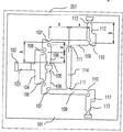
図14は、平行バネ構造を利用した従来の変位拡大装置の構成の一例を示す模式図である。
図14において、圧電素子1401が、基盤1402上に固定される。圧電素子1401の伸縮端側には、ボール1403が固定される。基盤1402上には、第1の弾性ヒンジ1404が配置され、第1の弾性ヒンジ1404には、圧電素子1401の出力軸と直交する方向に第1の梁1405が固定される。ボール1403は、第1の梁1405の任意の一点で接触する。第1の梁1405の自由端側には、第2の弾性ヒンジ1406が固定される。基盤1402の両側には、第3の弾性ヒンジ1407がそれぞれ1個づつ配置される。第3の弾性ヒンジ1407には、第2の梁1408が、それぞれ1本づつ、第1の梁1405と平行に固定される。第2の梁1408の自由端には、第4の弾性ヒンジ1409がそれぞれ1個づつ固定される。2個の第4の弾性ヒンジ1409には出力梁1410が固定される。出力梁1410の任意の位置に、第2の弾性ヒンジ1406が固定される。この変位拡大装置を2個、互いに直交するように組み合わせれば、XY方向の微小領域走査装置を構成することができる。
【0009】
図15は従来の変位拡大装置の動作を示した模式図である。
図15に、圧電素子1401が、紙面向かって右側にL1だけ伸びた状態を示す。この状態において、第1の梁1405は、ボール1403によって右側に向かって押され、第1の弾性ヒンジ1404を回転中心として傾く。このとき、第1の弾性ヒンジ1404とボール1403の間の距離をa、第1の弾性ヒンジ1404と第2の弾性ヒンジ1406の距離、すなわち、第1の梁1405の長さをbとする。第1の梁1405は、第1の弾性ヒンジ1404を支点とし、ボール1403を力点、第2の弾性ヒンジ1406を作用点とした梃子として作用し、圧電素子1401の伸び量がL1の時の第2の弾性ヒンジ1406の変位量L2は、L2=L1・b/aとなる。この第2の弾性ヒンジ1406の変位によって出力梁1410は、第2の弾性ヒンジ1406の変位と同じ変位量で右に動く。このときに、2本の第2の梁1408は出力梁1410を水平に保つ案内として作用する。
【0010】
【発明が解決しようとする課題】
【0011】
しかしながら、以上に示したような平行バネ構造を利用した従来の変位拡大装置においては、平行バネが支点を中心とした回転運動を行うことから、主変位方向とは別の方向にも回転による変位が発生してしまう。図15におけるΔhがこの回転による変位である。これは、梃子の拡大率を大きくするほど顕著である。さらに、このような変位拡大装置を1軸ないしは2軸用いて微小領域走査装置を構成し、走査型プローブ顕微鏡(SPM)に組み込んだ場合、観察像にゆがみが生じるなどの問題がある。
【0012】
そこで、本発明の目的は、従来の平行ばね構造を用いた変位拡大装置および微小領域走査装置の持つ上記のような課題を解決し、梃子による圧電素子の変位拡大率を大きくしつつ、主変位方向とは別の方向への変位が発生しない変位拡大装置を実現し、これを用いて観察像にゆがみを生じない微小領域走査装置を実現することにある。
【0013】
【課題を解決するための手段】
上記課題を解決するために、本発明では、走査型プローブ顕微鏡(SPM)の試料走査やプローブ走査用の微小領域走査装置に利用する変位拡大装置と、これを用いる微小領域走査装置において、圧電素子と組み合わせる平行ばね構造に、近似平行運動連鎖の構造を取り入れ、平行ばねの出力点が近似直線運動を行うようにした。さらにこの近似平行運動連鎖を2組向かい合わせて梁で結合することにより、角度変位のない近似直線変位を取り出せるようにした。加えて、この近似平行運動連鎖の1部に梃子の作用を兼ねさせることによって、圧電素子の変位を拡大し、この拡大変位が近似直線変位として得られるようにした。また、この変位拡大装置を組み合わせて微小領域走査装置を構成した。
【0014】
【発明の実施の形態】
以下に、本発明の実施例について図に基づいて説明する。
(1)第1の実施例
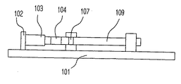
図1、図2は、本発明の変位拡大装置のうち、第1の実施例を示した模式図である。
【0015】
図1は上面図、図2は側面図を示す。図1、図2において、基盤101上の第1のホルダ102に、第1の圧電素子103の基部が固定される。
固定は、第1の圧電素子103の出力軸と基盤101が平行になるように、かつ、第1の圧電素子103の側面が基盤101に非接触である位置関係で行われる。第1の圧電素子103の伸縮端には、2股形状をした入力梁104が固定される。基盤101上には、圧電素子103の出力軸を基準として対称的に配置される2組の近似平行運動連鎖と、2組の近似平行運動連鎖の対向する2本の梁を結合する出力梁114が配置される。この2組の近似平行運動連鎖と出力梁114は、すべて基盤101の同一平面上に配置される。
【0016】
2組の近似平行運動連鎖のうち、1組の近似平行運動連鎖の構成を以下に説明する。
基盤101上に、基盤101と垂直をなす回転軸を有する第1の支点105が固定される。第1の支点105に、第1の梁106が回転自在に固定される。この第1の梁106は、第1の圧電素子103の出力軸と直交する方向に配置される。第1の梁106の自由端には、第1の回転対偶107が配置される。第1の梁106上の任意の位置に、第2の回転対偶108が固定される。支点および回転対偶は一体型切り欠き構造の弾性ヒンジによって構成される。弾性ヒンジの材質としては、SUS、リン青銅、ポリアセタールなど弾性の高いものを用いる。
【0017】
本実施例では、すべての回転対偶にSUSを用い、同形状の切り欠き構造としている。
ここで、第1の支点105から第2の回転対偶108までの距離を(c)とし、第1の回転対偶107から第2の回転対偶108までの距離を(d)としたときに、図1では、c:d=1:1となる位置に第2の回転対偶108が位置する。
【0018】
第1の回転対偶107には、第2の梁109が、第1の梁106と任意の角度を持って固定される。図1では、90°の角度を有している。第2の梁109の任意の位置に、第3の回転対偶110と、第4の回転対偶111が固定される。図1では、第3の回転対偶110が第2の梁109の端に固定され、第4の回転対偶111は、第1の回転対偶107と第3の回転対偶110の間の第2の梁109上の任意の位置に固定されている。第3の回転対偶110には、第3の梁112が、第1の梁106と平行に固定され、第3の梁112のもう一端は、基盤101と垂直を成す回転軸を有する第2の支点113に固定される。
【0019】
ここで、第1の梁106の長さを(A)、第3の梁112の長さを(B)とし、
第3の回転対偶110と第4の回転対偶111の間の距離を(a)、第1の回転対偶107と第4の回転対偶111の間の距離を(b)とした時に、A:B=a:bとなる位置関係を持たせる。
【0020】
以上が、1組の近似平行運動連鎖の構成であり、この近似平行運動連鎖が圧電素子103の出力軸を基準として基盤上に対称的に2組配置される。
2組の近似平行運動連鎖の対向する2本の梁、すなわち、2本の第2の梁109は、対向する2個の第4の回転対偶111を介して、出力梁114で固定される。
【0021】
2個の第2の回転対偶108には、2股形状の入力梁104の自由端が1本づつ固定される。
図3は、第1の実施例の動作を示した模式図である。
図3に、第1の圧電素子103が、紙面向かって右側にL1だけ伸びた状態を示す。この状態において、入力梁104がL1だけ右側に移動し、これに伴い第2の回転対偶108がL1だけ右側に移動する。第2の回転対偶108の移動に伴い、第1の梁106は、第1の支点105を軸として回転運動を行う。すなわち、第2の回転対偶108は、第1の圧電素子103の伸縮変位の入力点として作用し、これにより、第1の梁106は、第1の支点105を軸とした梃子として作用する。梃子の作用点は、第1の回転対偶107である。ここで、図1で説明したように、第1の支点105から第2の回転対偶108までの距離を(c)とし、第1の回転対偶107から第2の回転対偶108までの距離を(d)としたときに、図1では、c:d=1:1となる位置に第2の回転対偶108を配置する。この時の、第1の回転対偶107の出力変位量をL2とすれば、L2=L1・(c+d)/c=2・L1である。
【0022】
さらにここで、第1の支点105、第1の梁106、第1の回転対偶107、第2の梁109、第3の回転対偶110、第4の回転対偶111、第3の梁112、第2の支点113の関係を考える。図1で説明したように、第1の梁106の長さを(A)、第3の梁112の長さを(B)とし、第3の回転対偶110と第4の回転対偶111の間の距離を(a)、第1の回転対偶107と第4の回転対偶111の間の距離を(b)とした時に、A:B=a:bとなる位置関係が存在する。
【0023】
これはすなわち、第4の回転対偶111を出力点とするワットの近似平行運動連鎖である。したがって、第1の梁106の運動に伴い、第2の梁109、第3の梁112が連鎖運動し、第2の梁109上の第4の回転対偶111が近似直線運動を行う。このとき、第4の回転対偶111は、わずかではあるが角度変位しながら直線変位する。この第4の回転対偶111の出力変位をL3とすれば、L3≒L2である。
【0024】
本発明においては、このワットの近似平行運動連鎖を第1の圧電素子103の出力軸を基準として基盤上に対称的に2組配置し、対向する2個の第4の回転対偶111を、出力梁114で連結する。これによって、第4の回転対偶111の角度変位の影響は、第4の回転対偶111自体の弾性により吸収され、出力梁114から直線変位のみを取り出すことができる。同時に、この出力梁114は、2組の近似平行運動連鎖の剛性向上に貢献し、第2の梁109のねじれを防ぐ作用もある。出力梁114の変位出力方向は第1の圧電素子103の出力軸と同じ方向である。
【0025】
図4は、第1の実施例の各梁の断面図である。図4(a)は第1の梁106の第1の支点105付近の断面図であり、(b)は第3の梁112の第2の支点113付近の断面図で、同じ形状をしている。図4(c)は第2の梁109の第1の回転対偶107付近の断面図であり、図4(d)は、第2の梁109の第4の回転対偶111付近の断面図である。断面(a)、(b)、(c)、(d)は、断面形状および断面積を変化させることで、垂直方向の曲げ剛性が(a)=(b)=(c)=(d)であり、かつ、単位質量は(a)=(b)>(c)>(d)となるような質量勾配をを有する構成としている。質量勾配は連続的かつ滑らかである。すなわち、出力梁114に近づくにつれて剛性はそのままに質量が小さくなるように設定されており、これにより、自重による各梁のたわみ量を最小にすることができる。第1の実施例では、I型断面を利用しているが、丸形中空断面、角形中空断面を利用することも可能である。また、質量勾配を、断面積変化ではなく材質の成分変化によって実現することも可能である。
【0026】
図5は、図4で説明した梁の断面変化の状態を模式的に示した斜視図である。
(2) 第2の実施例
図6、図7は、本発明の変位拡大装置及びこれを用いた微小領域走査装置のうち、第2の実施例を示した模式図である。図6は上面図、図7は側面図を示す。図6、図7において、基盤101上の第1のホルダ102に、第1の圧電素子103の基部が固定される。固定は、第1の圧電素子103の出力軸と基盤101が平行になるように、かつ、第1の圧電素子103の側面が基盤101に非接触である位置関係で行われる。第1の圧電素子103の伸縮端には、2股形状の入力梁104が固定される。基盤101上には、第1の圧電素子103の出力軸を基準として対称的に配置される2組の近似平行運動連鎖と、2組の近似平行運動連鎖の対向する2本の梁を結合する出力梁114が配置される。この2組の近似平行運動連鎖と出力梁114は、すべて基盤101の同一平面上に配置される。出力梁114には第2のホルダー115が固定され、この第2のホルダー115に、第1の圧電素子103の出力軸と直交する出力軸を持つ第2の圧電素子116の基部が固定されている。固定は、第2の圧電素子116の出力軸と出力梁114が平行になるように、かつ、第2の圧電素子116の側面が出力梁114に非接触である位置関係で行われる。第2の圧電素子116の伸縮端には、試料台117が固定される。
【0027】
2組の近似平行運動連鎖のうち、1組の近似平行運動連鎖の構成を以下に説明する。
基盤101上に、基盤101と垂直をなす回転軸を有する第1の支点105が固定される。第1の支点105に、第1の梁106が回転自在に固定される。この第1の梁106は、第1の圧電素子103の出力軸と直交する方向に配置される。第1の梁106の自由端には、第1の回転対偶107が配置される。第1の梁106上の任意の位置に、第2の回転対偶108が固定される。支点および回転対偶は一体型切り欠き構造の弾性ヒンジによって構成される。弾性ヒンジの材質としては、SUS、リン青銅、ポリアセタールなど弾性の高いものを用いる。
【0028】
本実施例では、すべての回転対偶にSUSを用い、同形状の切り欠き構造としている。
ここで、第1の支点105から第2の回転対偶108までの距離を(c)とし、第1の回転対偶107から第2の回転対偶108までの距離を(d)としたときに、図6では、c:d=1:1となる位置に第2の回転対偶108を配置する。
【0029】
第1の回転対偶107には、第2の梁109が、第1の梁106と任意の角度を持って固定される。図6では、90ーの角度を有している。第2の梁109の任意の位置に、第3の回転対偶110と、第4の回転対偶111が固定される。
図6では、第4の回転対偶111が第2の梁109の端に固定され、第3の回転対偶110は、第1の回転対偶107と第4の回転対偶111の間の第2の梁109上の任意の位置に固定されている。この第3の回転対偶110と、第4の回転対偶111の位置が、第1の実施例とは異なる。第3の回転対偶110には、第3の梁112が、第1の梁106と平行に固定され、第3の梁112のもう一端は、基盤101と垂直を成す回転軸を有する第2の支点113に固定される。
【0030】
ここで、第1の梁106の長さを(A)、第3の梁112の長さを(B)とし、
第3の回転対偶110と第4の回転対偶111の間の距離を(a)、第1の回転対偶107と第4の回転対偶111の間の距離を(b)とした時に、A:B=a:bとなる位置関係を持たせる。
以上が、1組の近似平行運動連鎖の構成であり、この近似平行運動連鎖が第1の圧電素子103の出力軸を基準として基盤上に対称的に2組配置される。
【0031】
2組の近似平行運動連鎖の対向する2本の梁、すなわち、2本の第2の梁109は、対向する2個の第4の回転対偶111を介して、出力梁114で固定される。
2個の第2の回転対偶108には、2股形状の入力梁104の自由端が1本づつ固定される。
【0032】
図8は、第2の実施例の動作を示した模式図である。
図8に、第1の圧電素子103が、紙面向かって右側にL1だけ伸びた状態を示す。この状態において、入力梁104がL1だけ右側に移動し、これに伴い第2の回転対偶108がL1だけ右側に移動する。第2の回転対偶108の移動に伴い、第1の梁106は、第1の支点105を軸として回転運動を行う。すなわち、第2の回転対偶108は、第1の圧電素子103の伸縮変位の入力点として作用し、これにより、第1の梁106は、第1の支点105を軸としたテコとして作用する。テコの作用点は、第1の回転対偶107である。ここで、図6で説明したように、第1の支点105から第2の回転対偶108までの距離を(c)とし、第1の回転対偶107から第2の回転対偶108までの距離を(d)としたときに、c:d=1:1となる位置に第2の回転対偶108が位置する。この時の、第1の回転対偶107の出力変位量をL2とすれば、L2=L1・(c+d)/c=2・L1である。
【0033】
さらにここで、第1の支点105、第1の梁106、第1の回転対偶107、第2の梁109、第3の回転対偶110、第4の回転対偶111、第3の梁112、第2の支点113の関係を考える。図6で説明したように、第1の梁106の長さを(A)、第3の梁112の長さを(B)とし、第3の回転対偶110と第4の回転対偶111の間の距離を(a)、第1の回転対偶107と第4の回転対偶111の間の距離を(b)とした時に、A:B=a:bとなる位置関係が存在する。
【0034】
これはすなわち、第4の回転対偶111を出力点とするワットの近似平行運動連鎖である。したがって、第1の梁106の運動に伴い、第2の梁109、第3の梁112が連鎖運動し、第2の梁109上の第4の回転対偶111が近似直線運動を行う。このとき、第4の回転対偶111は、わずかではあるが角度変位しながら直線変位する。この第4の回転対偶111の出力変位をL3とすれば、L3≒L2である。
【0035】
本発明においては、このワットの近似平行運動連鎖を第1の圧電素子103の出力軸を基準として基盤上に対称的に2組配置し、対向する2個の第4の回転対偶111を、出力梁114で連結する。これによって、第4の回転対偶111の角度変位の影響は、第4の回転対偶111自体の弾性により吸収され、出力梁114から直線変位のみを取り出すことができる。同時に、この出力梁114は、2組の近似平行運動連鎖の剛性向上に貢献し、第2の梁109のねじれを防ぐ作用もある。出力梁114の変位出力方向は第1の圧電素子103の出力軸と同じ方向である。出力梁114の第2のホルダー115に固定されている第2の圧電素子116は、第1の圧電素子103の出力軸と直交する出力軸を持っており、この第2の圧電素子116を伸縮させることで、試料台117を移動させることができる。この例では、第2の圧電素子116をL4だけ伸ばした状態を示しており、この結果として、試料台117は、移動前の位置から右へL3、上にL4移動する。このように、第1の圧電素子103と第2の圧電素子116を別々に制御させることで、試料台117を2軸方向に走査することができる。
(3) 第3の実施例
図9、図10は、本発明の変位拡大装置およびこれを用いた微小領域走査装置のうち、第3の実施例を示した模式図である。図9は上面図、図10は側面図を示す。図9、図10において、変位拡大装置201の出力梁114に、第2の変位拡大装置202の基盤101が固定される。第1の変位拡大装置201と第2の変位拡大装置202は、第1の実施例または第2の実施例で述べた変位拡大装置と同じ構成をしている。第1の変位拡大装置201と第2の変位拡大装置202の出力軸方向は直交しており、第2の変位拡大装置202の出力梁114には、試料台117が固定される。
【0036】
図11は、第3の実施例の動作を示した模式図である。
図11に、第1の変位拡大装置201の第1の圧電素子103が、紙面向かって右側にL1だけ伸び、かつ、第2の変位拡大装置第1の202の圧電素子103が、紙面向かって上側にL1だけ伸びた状態を示す。この状態において、第1の変位拡大装置201の出力梁114は右側にL3変位し、これにより、第2の変位拡大装置202が右側にL3移動する。同時に、第2の変位拡大装置202の出力梁114は上側にL3伸びる。この結果として、第2の変位拡大装置202の出力梁114に固定されている試料台117は、移動前の位置から右にL3、上にL3、移動する。
(4) 第4の実施例
図12、図13は、本発明の変位拡大装置およびこれを用いた微小領域走査装置のうち、第4の実施例を示した模式図である。図12は上面図、図13は側面図を示す。図12、図13において、変位拡大装置201の出力梁114に、第2の変位拡大装置202の基盤101が固定される。第1の変位拡大装置201と第2の変位拡大装置202は、第1の実施例または第2の実施例で述べた変位拡大装置と同じ構成をしている。第1の変位拡大装置201と第2の変位拡大装置202の出力軸は直交しており、第2の変位拡大装置202の出力梁114には、第3のホルダ118が固定され、この上にZ軸用圧電素子119が固定されている。Z軸用圧電素子119の伸縮端には、試料台117が固定される。
【0037】
【発明の効果】
この発明は、以上説明したように、走査型プローブ顕微鏡(SPM)の試料走査やプローブ走査用の微小領域走査装置に利用される変位拡大装置およびこれを用いた微小領域走査装置において、基盤と、基盤に平行に固定される圧電素子と、圧電素子の伸縮端に基盤と平行に固定される入力梁と、圧電素子の出力軸を基準として対称的に配置される2組の近似平行運動連鎖と、2組の近似平行運動連鎖の対向する2本の梁を結合する出力梁により変位拡大装置を構成し、また、この変位拡大装置を用いて微小領域走査装置を構成した。
【0038】
上記のような構成としたので、以下に記載する効果を有する。
(1) 変位拡大装置の平行バネ構造に、近似平行運動連鎖の構造を取り入れることにより、平行バネの出力点に近似直線運動を行わせることができ、さらにこの近似平行運動連鎖を2組向かい合わせて梁で結合することにより、角度変位のない近似直線変位を取り出せる。
(2) 加えて、この近似平行運動連鎖の1部に梃子の作用を兼ねさせることによって、圧電素子の変位を拡大し、この拡大変位が近似直線変位として得られる。
(3) この変位拡大装置を組み合わせて微小領域走査装置を構成することで、梃子による圧電素子の変位拡大率を大きくしつつ、主変位方向とは別の方向への変位が発生しない変位拡大装置を実現し、さらに、これを用いて観察像にゆがみを生じない微小領域走査装置を実現することができる。
【図面の簡単な説明】
【図1】本発明の変位拡大装置のうち、第1の実施例の構成の一例を示した模式図である。
【図2】本発明の変位拡大装置のうち、第1の実施例の構成の一例を示した模式図である。
【図3】 本発明の変位拡大装置のうち、第1の実施例の動作を示した模式図である。
【図4】本発明の変位拡大装置のうち、第1の実施例の梁の断面図である。
【図5】本発明の変位拡大装置のうち、第1の実施例の梁の斜視図である。
【図6】本発明の変位拡大装置およびこれを用いた微小領域走査装置のうち、第2の実施例の構成の一例を示した模式図である。
【図7】本発明の変位拡大装置およびこれを用いた微小領域走査装置のうち、第2の実施例の構成の一例を示した模式図である。
【図8】本発明の変位拡大装置およびこれを用いた微小領域走査装置のうち、第2の実施例の動作を示した模式図である。
【図9】本発明の変位拡大装置およびこれを用いた微小領域走査装置のうち、第3の実施例の構成の一例を示した模式図である。
【図10】本発明の変位拡大装置およびこれを用いた微小領域走査装置のうち、第3の実施例の構成の一例を示した模式図である。
【図11】本発明の変位拡大装置およびこれを用いた微小領域走査装置のうち、第3の実施例の動作を示した模式図である。
【図12】本発明の変位拡大装置およびこれを用いた微小領域走査装置のうち、第4の実施例の構成の一例を示した模式図である。
【図13】本発明の変位拡大装置およびこれを用いた微小領域走査装置のうち、第4の実施例の構成の一例を示した模式図である。
【図14】本発明に関わる従来の微小領域走査装置の構成の一例を示す模式図である。
【図15】本発明に関わる従来の微小領域走査装置の動作を示した模式図である。
【符号の説明】
101 基盤
102 第1のホルダ
103 第1の圧電素子
104 入力梁
105 第1の支点
106 第1の梁
107 第1の回転対偶
108 第2の回転対偶
109 第2の梁
110 第3の回転対偶
111 第4の回転対偶
112 第3の梁
113 第2の支点
114 出力梁
115 第2のホルダ
116 第2の圧電素子
117 試料台
118 第3のホルダ
119 Z軸用圧電素子
201 第1の変位拡大装置
202 第2の変位拡大装置
1401 圧電素子
1402 基盤
1403 ボール
1404 第1の弾性ヒンジ
1405 第1の梁
1406 第2の弾性ヒンジ
1407 第3の弾性ヒンジ
1408 第2の梁
1409 第4の弾性ヒンジ
1410 出力梁[0001]
BACKGROUND OF THE INVENTION
The present invention is a displacement enlargement used for a micro area scanning apparatus used for sample scanning and probe scanning of a scanning probe microscope (SPM) represented by an atomic force microscope (AFM) and a scanning near field microscope (SNOM). The present invention relates to an apparatus and a micro area scanning apparatus using the same.
[0002]
[Prior art]
A scanning probe microscope (SPM) scans the surface of a sample with a mechanical probe (hereinafter referred to as a probe) and detects the interaction between the probe and the sample surface, thereby changing the physical quantity of the sample surface to nm. (10-9m) An apparatus for observing in the order of the following. For example, in a typical atomic force microscope (AFM) as one of the scanning probe microscopes (SPM), an atomic force acting between the probe and the sample surface is detected by information of a change in the deflection amount of the probe, and this is detected. By utilizing this, the surface shape of the sample can be observed.
[0003]
In such an apparatus, a mechanical device necessary for scanning a sample or a probe in a horizontal direction (hereinafter referred to as an XY direction) or in a horizontal direction and a height direction (hereinafter referred to as a Z direction) is a micro area scanning apparatus.
[0004]
A micro-region scanning apparatus used in a scanning probe microscope (SPM) requires a high resolution of 0.01 to 0.1 nm, and therefore a piezoelectric element is used. A typical example is a tube-type micro-region scanning apparatus as disclosed in US Pat. No. 5,306,919 (Elings et al.). At the beginning of the development of a scanning probe microscope (SPM), atomic images and the like are observed using such a micro-region scanning apparatus.
[0005]
Such a tube-type micro area scanning device has the advantages that the structure is simple and the resonance frequency is high when the amount of displacement is about ˜20 μm. However, when a displacement amount of, for example, 50 μm or more is required, the tube length increases, the resonance frequency decreases, and at the same time, the pitching during XY scanning increases. .
[0006]
In recent years, the spread of scanning probe microscopes (SPM) has spread, and observation of larger samples such as biological cells has been required, and movement amounts in the XY directions of 50 to 200 μm have been required. In addition, since observation on a normal optical microscope is also required, a micro-area scanning device that is thin in the Z direction is required. Along with this trend, instead of the conventional tube type, a displacement enlarging device that expands the displacement of the piezoelectric element several times by a combination of a piezoelectric element, an elastic hinge and an insulator, and a thin micro area scanning device using the displacement enlarging device Is produced.
[0007]
Such a displacement enlarging apparatus and a micro area scanning apparatus using the same are disclosed in, for example, US Pat. No. 5,051,594 (Tsuda et al.). The displacement magnifying device disclosed here is a formally applied lever principle to a structure called a parallel spring. In this example, an elastic hinge is used instead of a leaf spring. In such a displacement enlarging apparatus, a parallel spring that also serves as an insulator is inclined with a displacement of the piezoelectric element, and a displacement enlarged about 5 to 10 times can be obtained on the stage surface.
[0008]
FIG. 14 is a schematic diagram showing an example of the configuration of a conventional displacement enlarging device using a parallel spring structure.
In FIG. 14, the
[0009]
FIG. 15 is a schematic view showing the operation of a conventional displacement magnifying device.
FIG. 15 shows a state in which the
[0010]
[Problems to be solved by the invention]
[0011]
However, in the conventional displacement magnifying device using the parallel spring structure as described above, the parallel spring performs a rotational motion around the fulcrum, so that the displacement due to the rotation is also different from the main displacement direction. Will occur. Δh in FIG. 15 is the displacement due to this rotation. This is more conspicuous as the enlargement ratio of the insulator is increased. Furthermore, when such a displacement magnifying device is used in one or two axes to form a micro-region scanning device and incorporated in a scanning probe microscope (SPM), there is a problem that the observed image is distorted.
[0012]
Accordingly, an object of the present invention is to solve the above-mentioned problems of the displacement enlarging device and the micro-region scanning device using the conventional parallel spring structure, while increasing the displacement enlarging rate of the piezoelectric element by the insulator, An object of the present invention is to realize a displacement magnifying device that does not cause displacement in a direction different from the direction, and to use this to realize a micro-region scanning device that does not distort an observed image.
[0013]
[Means for Solving the Problems]
In order to solve the above-described problems, in the present invention, a displacement enlarging device used for a sample scanning or probe scanning micro region scanning device of a scanning probe microscope (SPM), and a micro region scanning device using the displacement enlarging device The parallel spring structure is combined with an approximate parallel motion chain structure so that the output point of the parallel spring performs approximate linear motion. Furthermore, two sets of these approximate parallel motion chains are faced to each other and connected by beams so that approximate linear displacement without angular displacement can be extracted. In addition, the displacement of the piezoelectric element is expanded by making a part of the approximate parallel motion chain also function as an insulator so that the expanded displacement can be obtained as an approximate linear displacement. In addition, a micro-region scanning device is configured by combining this displacement magnifying device.
[0014]
DETAILED DESCRIPTION OF THE INVENTION
Embodiments of the present invention will be described below with reference to the drawings.
(1) First embodiment
1 and 2 are schematic views showing a first embodiment of the displacement magnifying device of the present invention.
[0015]
1 is a top view and FIG. 2 is a side view. 1 and 2, the base of the first
The fixing is performed such that the output shaft of the first
[0016]
Of the two sets of approximate parallel motion chains, the configuration of one set of approximate parallel motion chains will be described below.
A
[0017]
In the present embodiment, SUS is used for all the rotation pairs, and the cutout structure has the same shape.
Here, when the distance from the
[0018]
A
[0019]
Here, the length of the
When the distance between the third
[0020]
The above is the configuration of one set of approximate parallel motion chains, and two sets of these approximate parallel motion chains are symmetrically arranged on the base with the output axis of the
Two opposing beams of two sets of approximate parallel motion chains, that is, two
[0021]
One free end of the
FIG. 3 is a schematic diagram showing the operation of the first embodiment.
FIG. 3 shows a state in which the first
[0022]
Further, here, the
[0023]
In other words, this is an approximate parallel motion chain of watts with the fourth
[0024]
In the present invention, two sets of the approximate parallel motion chain of watts are symmetrically arranged on the base with respect to the output axis of the first
[0025]
FIG. 4 is a sectional view of each beam in the first embodiment. 4A is a cross-sectional view of the
[0026]
FIG. 5 is a perspective view schematically showing the state of cross-sectional change of the beam described in FIG.
(2) Second embodiment
6 and 7 are schematic views showing a second embodiment of the displacement magnifying device of the present invention and the micro area scanning device using the same. 6 shows a top view and FIG. 7 shows a side view. 6 and 7, the base of the first
[0027]
Of the two sets of approximate parallel motion chains, the configuration of one set of approximate parallel motion chains will be described below.
A
[0028]
In the present embodiment, SUS is used for all the rotation pairs, and the cutout structure has the same shape.
Here, when the distance from the
[0029]
A
In FIG. 6, the fourth
[0030]
Here, the length of the
When the distance between the third
The above is the configuration of one set of approximate parallel motion chains, and these two sets of approximate parallel motion chains are symmetrically arranged on the base with the output axis of the first
[0031]
Two opposing beams of two sets of approximate parallel motion chains, that is, two
One free end of the
[0032]
FIG. 8 is a schematic diagram showing the operation of the second embodiment.
FIG. 8 shows a state in which the first
[0033]
Further, here, the
[0034]
In other words, this is an approximate parallel motion chain of watts with the fourth
[0035]
In the present invention, two sets of the approximate parallel motion chain of watts are symmetrically arranged on the base with respect to the output axis of the first
(3) Third embodiment
FIGS. 9 and 10 are schematic views showing a third embodiment of the displacement magnifying device of the present invention and the micro area scanning device using the same. 9 shows a top view and FIG. 10 shows a side view. 9 and 10, the
[0036]
FIG. 11 is a schematic diagram showing the operation of the third embodiment.
In FIG. 11, the first
(4) Fourth embodiment
12 and 13 are schematic views showing a fourth embodiment of the displacement magnifying device of the present invention and the micro area scanning device using the same. 12 shows a top view and FIG. 13 shows a side view. 12 and 13, the
[0037]
【The invention's effect】
As described above, the present invention provides a displacement enlarging device used for a micro scanning device for scanning a sample and scanning a probe of a scanning probe microscope (SPM), and a micro scanning device using the same. A piezoelectric element fixed in parallel to the base, an input beam fixed in parallel to the base to the expansion / contraction end of the piezoelectric element, and two sets of approximate parallel motion chains arranged symmetrically with respect to the output axis of the piezoelectric element A displacement magnifying device was constituted by an output beam connecting two opposing beams of two sets of approximate parallel motion chains, and a micro area scanning device was constituted by using this displacement magnifying device.
[0038]
Since it was set as the above structures, it has the effect described below.
(1) By adopting an approximate parallel motion chain structure in the parallel spring structure of the displacement magnifying device, it is possible to cause the output point of the parallel spring to perform approximate linear motion, and two pairs of this approximate parallel motion chain face each other. By connecting with beams, approximate linear displacement without angular displacement can be extracted.
(2) In addition, by making a part of this approximate parallel motion chain also function as an insulator, the displacement of the piezoelectric element is enlarged, and this enlarged displacement is obtained as an approximate linear displacement.
(3) Displacement enlarging apparatus that does not generate displacement in a direction different from the main displacement direction while increasing the displacement enlarging rate of the piezoelectric element by the insulator by combining the displacement enlarging apparatus to constitute a micro area scanning apparatus. Furthermore, by using this, it is possible to realize a micro-area scanning device that does not distort the observed image.
[Brief description of the drawings]
FIG. 1 is a schematic diagram showing an example of the configuration of a first embodiment of a displacement magnifying apparatus according to the present invention.
FIG. 2 is a schematic diagram showing an example of the configuration of the first embodiment of the displacement magnifying device of the present invention.
FIG. 3 is a schematic diagram showing the operation of the first embodiment of the displacement magnifying device of the present invention.
FIG. 4 is a cross-sectional view of a beam according to a first embodiment of the displacement magnifying device of the present invention.
FIG. 5 is a perspective view of the beam of the first embodiment of the displacement magnifying device of the present invention.
FIG. 6 is a schematic diagram showing an example of the configuration of a second embodiment of the displacement magnifying device of the present invention and the micro area scanning device using the same.
FIG. 7 is a schematic view showing an example of the configuration of a second embodiment of the displacement magnifying device of the present invention and the micro area scanning device using the same.
FIG. 8 is a schematic diagram showing the operation of the second embodiment of the displacement magnifying device of the present invention and the micro area scanning device using the same.
FIG. 9 is a schematic view showing an example of the configuration of a third embodiment of the displacement magnifying device of the present invention and the micro area scanning device using the same.
FIG. 10 is a schematic view showing an example of the configuration of a third embodiment of the displacement magnifying device of the present invention and the micro area scanning device using the same.
FIG. 11 is a schematic diagram showing the operation of the third embodiment of the displacement magnifying device of the present invention and the micro area scanning device using the same.
FIG. 12 is a schematic view showing an example of the configuration of a fourth embodiment of the displacement magnifying device of the present invention and the micro area scanning device using the same.
FIG. 13 is a schematic view showing an example of the configuration of a fourth embodiment of the displacement magnifying device of the present invention and the micro area scanning device using the same.
FIG. 14 is a schematic diagram showing an example of the configuration of a conventional micro area scanning apparatus according to the present invention.
FIG. 15 is a schematic diagram showing the operation of a conventional micro area scanning apparatus according to the present invention.
[Explanation of symbols]
101 base
102 first holder
103 1st piezoelectric element
104 Input beam
105 First fulcrum
106 First beam
107 First rotation pair
108 Second rotating pair
109 Second beam
110 Third rotation pair
111 4th rotating pair
112 Third beam
113 Second fulcrum
114 Output beam
115 second holder
116 Second piezoelectric element
117 Sample stage
118 Third holder
119 Z-axis piezoelectric element
201 First displacement magnifying device
202 Second displacement magnifying device
1401 Piezoelectric element
1402 Foundation
1403 balls
1404 First elastic hinge
1405 First beam
1406 Second elastic hinge
1407 Third elastic hinge
1408 2nd beam
1409 fourth elastic hinge
1410 Output beam
Claims (6)
a) 前記2組の近似平行運動連鎖のそれぞれ1組は、
前記基盤上に固定され、前記基板と垂直をなす回転軸を有する第1の支点と、
前記第1の支点に回転自在に固定され、前記圧電素子の出力軸と直交する方向に延びる第1の梁と、
前記第1の梁の自由端に固定される第1の回転対偶と、
前記第1の梁に固定され、前記第1の支点と自由端の間の任意の一点に位置する第2の回転対偶と、
前記第1の回転対偶に、前記第1の梁と任意の角度を持って固定される第2の
梁と、
前記第2の梁の任意の位置に固定される第3の回転対偶と、
前記第2の梁の任意の位置に固定される第4の回転対偶と、
前記第3の回転対偶に固定され、第1の梁と平行に配置される第3の梁と、
第3の梁のもう一端を回転自在に固定し、前記基盤上に固定され、前記基盤と垂直をなす回転軸を有する第2の支点と、
を含み、同時に、
b) 前記第1の梁の長さ(A)と前記第3の梁の長さ(B)との比が、前記第3の回転対偶と前記第4の回転対偶の間の距離(a)と、前記第1の回転対偶と前記第4の回転対偶の間の距離(b)との比に等しい、すなわち、A:B=a:bになる位置関係にあり、
c) 前記入力梁が前記第2の回転対偶に固定され、前記出力梁の両端が前記2組の近似平行運動連鎖の対向する2個の前記第4の回転対偶に固定されることを特徴とする変位拡大装置。 A base, a piezoelectric element fixed in parallel to the base, an input beam fixed in parallel to the base to the extendable end of the piezoelectric element, and a symmetrical arrangement with respect to the output axis of the piezoelectric element 2 A displacement magnifying device comprising a pair of approximate parallel motion chains and an output beam connecting the two opposing beams of the two pairs of approximate parallel motion chains ;
a) Each of the two sets of approximate parallel motion chains is
A first fulcrum fixed on the substrate and having a rotation axis perpendicular to the substrate;
A first beam rotatably fixed to the first fulcrum and extending in a direction perpendicular to the output axis of the piezoelectric element;
A first rotating pair fixed to the free end of the first beam;
A second rotating pair fixed to the first beam and located at any one point between the first fulcrum and a free end;
The second rotating pair is fixed at an arbitrary angle with the first beam.
The beam,
A third rotating pair fixed to an arbitrary position of the second beam;
A fourth rotating pair fixed to an arbitrary position of the second beam;
A third beam fixed to the third rotating pair and disposed in parallel with the first beam;
A second fulcrum fixed to the other end of the third beam so as to be rotatable, fixed on the base and having a rotation axis perpendicular to the base;
At the same time,
b) The ratio of the length of the first beam (A) to the length of the third beam (B) is the distance between the third rotating pair and the fourth rotating pair (a) And a ratio of the distance (b) between the first rotation pair and the fourth rotation pair, i.e., A: B = a: b.
c) The input beam is fixed to the second rotating pair, and both ends of the output beam are fixed to two opposing fourth rotating pairs of the two sets of approximate parallel motion chains. Displacement magnifying device.
Priority Applications (1)
| Application Number | Priority Date | Filing Date | Title |
|---|---|---|---|
| JP05391098A JP3897893B2 (en) | 1998-03-05 | 1998-03-05 | Displacement magnifying device and micro area scanning device using the same |
Applications Claiming Priority (1)
| Application Number | Priority Date | Filing Date | Title |
|---|---|---|---|
| JP05391098A JP3897893B2 (en) | 1998-03-05 | 1998-03-05 | Displacement magnifying device and micro area scanning device using the same |
Publications (2)
| Publication Number | Publication Date |
|---|---|
| JPH11248719A JPH11248719A (en) | 1999-09-17 |
| JP3897893B2 true JP3897893B2 (en) | 2007-03-28 |
Family
ID=12955882
Family Applications (1)
| Application Number | Title | Priority Date | Filing Date |
|---|---|---|---|
| JP05391098A Expired - Fee Related JP3897893B2 (en) | 1998-03-05 | 1998-03-05 | Displacement magnifying device and micro area scanning device using the same |
Country Status (1)
| Country | Link |
|---|---|
| JP (1) | JP3897893B2 (en) |
Families Citing this family (6)
| Publication number | Priority date | Publication date | Assignee | Title |
|---|---|---|---|---|
| JP4343879B2 (en) * | 1999-09-27 | 2009-10-14 | キヤノン株式会社 | Cutting method |
| JP3815789B1 (en) * | 2005-03-11 | 2006-08-30 | 株式会社マコメ研究所 | Displacement transmission device |
| JP4958139B2 (en) * | 2006-02-14 | 2012-06-20 | 日置電機株式会社 | Displacement magnifying mechanism with displacement final output end and processing apparatus provided with the displacement magnifying mechanism |
| JP5487462B2 (en) * | 2008-07-11 | 2014-05-07 | 国立大学法人秋田大学 | Actuation type displacement magnifying device |
| CN102904481A (en) * | 2012-03-08 | 2013-01-30 | 中南大学 | Spiral compact displacement amplifying device |
| CN107131404B (en) * | 2017-04-24 | 2019-03-19 | 天津大学 | It is single to drive the pure rotation mini positioning platform of double pendulum type |
-
1998
- 1998-03-05 JP JP05391098A patent/JP3897893B2/en not_active Expired - Fee Related
Also Published As
| Publication number | Publication date |
|---|---|
| JPH11248719A (en) | 1999-09-17 |
Similar Documents
| Publication | Publication Date | Title |
|---|---|---|
| US5705878A (en) | Flat scanning stage for scanned probe microscopy | |
| US5107114A (en) | Fine scanning mechanism for atomic force microscope | |
| US7372025B2 (en) | Scanning probe microscope using a surface drive actuator to position the scanning tip | |
| US7690047B2 (en) | Scanning probe apparatus | |
| EP2201421A1 (en) | Mems scanning micromirror with reduced dynamic deformation | |
| JP4789162B2 (en) | Actuator using comb teeth | |
| JP3897893B2 (en) | Displacement magnifying device and micro area scanning device using the same | |
| JP5605227B2 (en) | Planar positioning device and inspection device provided with the same | |
| US8028567B2 (en) | AFM tweezers, method for producing AFM tweezers, and scanning probe microscope | |
| US5223713A (en) | Scanner for scanning tunneling microscope | |
| US6194813B1 (en) | Extended-range xyz linear piezo-mechanical scanner for scanning-probe and surface force applications | |
| Xu et al. | Microelectromechanical scanning tunneling microscope | |
| US20070085022A1 (en) | Scanning mechanism for scanning probe microscope | |
| Akiyama et al. | Atomic force microscopy using an integrated comb-shape electrostatic actuator for high-speed feedback motion | |
| JP2000009867A (en) | Stage moving device | |
| JP2006220597A (en) | Surface information measurement device | |
| WO2006057300A1 (en) | Positioning mechanism and microscope using the same | |
| Tapson et al. | A simple dynamic piezoelectric X‐Y translation stage suitable for scanning probe microscopes | |
| KR101151136B1 (en) | Scanner for scanning probe microscope | |
| JP3369892B2 (en) | Positioning device for micro positioning device | |
| Cai et al. | An alternative flat scanner and micropositioning method for scanning probe microscope | |
| JP4280382B2 (en) | Information detecting apparatus and information detecting method having scanning probe | |
| JP4276890B2 (en) | Scanning mechanism and scanning probe microscope using the same | |
| McCord | An x-y-z stage for scanning proximity microscopes using elastic elements | |
| JP2001133382A (en) | Scanning probe microscope |
Legal Events
| Date | Code | Title | Description |
|---|---|---|---|
| RD01 | Notification of change of attorney |
Free format text: JAPANESE INTERMEDIATE CODE: A7421 Effective date: 20040302 |
|
| A521 | Request for written amendment filed |
Free format text: JAPANESE INTERMEDIATE CODE: A523 Effective date: 20040414 |
|
| A621 | Written request for application examination |
Free format text: JAPANESE INTERMEDIATE CODE: A621 Effective date: 20040414 |
|
| A131 | Notification of reasons for refusal |
Free format text: JAPANESE INTERMEDIATE CODE: A131 Effective date: 20061003 |
|
| A521 | Request for written amendment filed |
Free format text: JAPANESE INTERMEDIATE CODE: A523 Effective date: 20061129 |
|
| TRDD | Decision of grant or rejection written | ||
| A01 | Written decision to grant a patent or to grant a registration (utility model) |
Free format text: JAPANESE INTERMEDIATE CODE: A01 Effective date: 20061219 |
|
| A61 | First payment of annual fees (during grant procedure) |
Free format text: JAPANESE INTERMEDIATE CODE: A61 Effective date: 20061220 |
|
| R150 | Certificate of patent or registration of utility model |
Free format text: JAPANESE INTERMEDIATE CODE: R150 |
|
| FPAY | Renewal fee payment (event date is renewal date of database) |
Free format text: PAYMENT UNTIL: 20110105 Year of fee payment: 4 |
|
| FPAY | Renewal fee payment (event date is renewal date of database) |
Free format text: PAYMENT UNTIL: 20110105 Year of fee payment: 4 |
|
| RD03 | Notification of appointment of power of attorney |
Free format text: JAPANESE INTERMEDIATE CODE: R3D03 |
|
| FPAY | Renewal fee payment (event date is renewal date of database) |
Free format text: PAYMENT UNTIL: 20110105 Year of fee payment: 4 |
|
| FPAY | Renewal fee payment (event date is renewal date of database) |
Free format text: PAYMENT UNTIL: 20120105 Year of fee payment: 5 |
|
| FPAY | Renewal fee payment (event date is renewal date of database) |
Free format text: PAYMENT UNTIL: 20130105 Year of fee payment: 6 |
|
| FPAY | Renewal fee payment (event date is renewal date of database) |
Free format text: PAYMENT UNTIL: 20140105 Year of fee payment: 7 |
|
| S111 | Request for change of ownership or part of ownership |
Free format text: JAPANESE INTERMEDIATE CODE: R313113 |
|
| R350 | Written notification of registration of transfer |
Free format text: JAPANESE INTERMEDIATE CODE: R350 |
|
| R250 | Receipt of annual fees |
Free format text: JAPANESE INTERMEDIATE CODE: R250 |
|
| R250 | Receipt of annual fees |
Free format text: JAPANESE INTERMEDIATE CODE: R250 |
|
| R250 | Receipt of annual fees |
Free format text: JAPANESE INTERMEDIATE CODE: R250 |
|
| LAPS | Cancellation because of no payment of annual fees |