JP3892588B2 - Semiconductor device and manufacturing method thereof - Google Patents
Semiconductor device and manufacturing method thereof Download PDFInfo
- Publication number
- JP3892588B2 JP3892588B2 JP18530298A JP18530298A JP3892588B2 JP 3892588 B2 JP3892588 B2 JP 3892588B2 JP 18530298 A JP18530298 A JP 18530298A JP 18530298 A JP18530298 A JP 18530298A JP 3892588 B2 JP3892588 B2 JP 3892588B2
- Authority
- JP
- Japan
- Prior art keywords
- insulating film
- gate electrode
- gate
- film
- source
- Prior art date
- Legal status (The legal status is an assumption and is not a legal conclusion. Google has not performed a legal analysis and makes no representation as to the accuracy of the status listed.)
- Expired - Fee Related
Links
- 239000004065 semiconductor Substances 0.000 title claims description 44
- 238000004519 manufacturing process Methods 0.000 title claims description 22
- 239000010410 layer Substances 0.000 claims description 74
- 239000000758 substrate Substances 0.000 claims description 74
- 238000009792 diffusion process Methods 0.000 claims description 69
- 238000000034 method Methods 0.000 claims description 57
- 239000011229 interlayer Substances 0.000 claims description 25
- 238000002955 isolation Methods 0.000 claims description 19
- 230000015572 biosynthetic process Effects 0.000 claims description 18
- 108091006146 Channels Proteins 0.000 description 90
- XUIMIQQOPSSXEZ-UHFFFAOYSA-N Silicon Chemical compound [Si] XUIMIQQOPSSXEZ-UHFFFAOYSA-N 0.000 description 42
- 229910052710 silicon Inorganic materials 0.000 description 40
- 239000010703 silicon Substances 0.000 description 40
- 239000012535 impurity Substances 0.000 description 33
- 230000000694 effects Effects 0.000 description 20
- 229910052751 metal Inorganic materials 0.000 description 16
- 239000002184 metal Substances 0.000 description 16
- 238000005468 ion implantation Methods 0.000 description 13
- 238000005530 etching Methods 0.000 description 12
- VYPSYNLAJGMNEJ-UHFFFAOYSA-N Silicium dioxide Chemical compound O=[Si]=O VYPSYNLAJGMNEJ-UHFFFAOYSA-N 0.000 description 9
- 238000001020 plasma etching Methods 0.000 description 9
- 229910021420 polycrystalline silicon Inorganic materials 0.000 description 9
- LIVNPJMFVYWSIS-UHFFFAOYSA-N silicon monoxide Chemical compound [Si-]#[O+] LIVNPJMFVYWSIS-UHFFFAOYSA-N 0.000 description 9
- 229910052681 coesite Inorganic materials 0.000 description 8
- 229910052906 cristobalite Inorganic materials 0.000 description 8
- 230000007423 decrease Effects 0.000 description 8
- 229920005591 polysilicon Polymers 0.000 description 8
- 239000000377 silicon dioxide Substances 0.000 description 8
- 229910052682 stishovite Inorganic materials 0.000 description 8
- 229910052905 tridymite Inorganic materials 0.000 description 8
- 238000010438 heat treatment Methods 0.000 description 7
- 239000000463 material Substances 0.000 description 7
- ATJFFYVFTNAWJD-UHFFFAOYSA-N Tin Chemical compound [Sn] ATJFFYVFTNAWJD-UHFFFAOYSA-N 0.000 description 5
- 230000006866 deterioration Effects 0.000 description 5
- 229920002120 photoresistant polymer Polymers 0.000 description 5
- 229910052814 silicon oxide Inorganic materials 0.000 description 5
- 238000001994 activation Methods 0.000 description 4
- 230000015556 catabolic process Effects 0.000 description 4
- 238000009413 insulation Methods 0.000 description 4
- 238000001459 lithography Methods 0.000 description 4
- UFHFLCQGNIYNRP-UHFFFAOYSA-N Hydrogen Chemical compound [H][H] UFHFLCQGNIYNRP-UHFFFAOYSA-N 0.000 description 3
- 230000001133 acceleration Effects 0.000 description 3
- 230000004913 activation Effects 0.000 description 3
- 238000006243 chemical reaction Methods 0.000 description 3
- 238000000151 deposition Methods 0.000 description 3
- 238000010586 diagram Methods 0.000 description 3
- 229910052739 hydrogen Inorganic materials 0.000 description 3
- 239000001257 hydrogen Substances 0.000 description 3
- 238000007254 oxidation reaction Methods 0.000 description 3
- 238000004151 rapid thermal annealing Methods 0.000 description 3
- 229910052721 tungsten Inorganic materials 0.000 description 3
- 239000010937 tungsten Substances 0.000 description 3
- 229910008479 TiSi2 Inorganic materials 0.000 description 2
- 229910008814 WSi2 Inorganic materials 0.000 description 2
- 238000005229 chemical vapour deposition Methods 0.000 description 2
- 150000002500 ions Chemical class 0.000 description 2
- 239000012528 membrane Substances 0.000 description 2
- 230000003647 oxidation Effects 0.000 description 2
- 230000003071 parasitic effect Effects 0.000 description 2
- 230000002093 peripheral effect Effects 0.000 description 2
- 229910021332 silicide Inorganic materials 0.000 description 2
- FVBUAEGBCNSCDD-UHFFFAOYSA-N silicide(4-) Chemical compound [Si-4] FVBUAEGBCNSCDD-UHFFFAOYSA-N 0.000 description 2
- 239000002356 single layer Substances 0.000 description 2
- -1 tungsten nitride Chemical class 0.000 description 2
- 230000005641 tunneling Effects 0.000 description 2
- 229910018182 Al—Cu Inorganic materials 0.000 description 1
- ZOXJGFHDIHLPTG-UHFFFAOYSA-N Boron Chemical compound [B] ZOXJGFHDIHLPTG-UHFFFAOYSA-N 0.000 description 1
- 108010075750 P-Type Calcium Channels Proteins 0.000 description 1
- OAICVXFJPJFONN-UHFFFAOYSA-N Phosphorus Chemical compound [P] OAICVXFJPJFONN-UHFFFAOYSA-N 0.000 description 1
- 229910004298 SiO 2 Inorganic materials 0.000 description 1
- 230000003213 activating effect Effects 0.000 description 1
- 230000001154 acute effect Effects 0.000 description 1
- 238000000137 annealing Methods 0.000 description 1
- 229910052785 arsenic Inorganic materials 0.000 description 1
- RQNWIZPPADIBDY-UHFFFAOYSA-N arsenic atom Chemical compound [As] RQNWIZPPADIBDY-UHFFFAOYSA-N 0.000 description 1
- 229910052796 boron Inorganic materials 0.000 description 1
- 239000003990 capacitor Substances 0.000 description 1
- 230000003247 decreasing effect Effects 0.000 description 1
- 238000000280 densification Methods 0.000 description 1
- 230000008021 deposition Effects 0.000 description 1
- 230000002542 deteriorative effect Effects 0.000 description 1
- 230000005684 electric field Effects 0.000 description 1
- 239000007789 gas Substances 0.000 description 1
- 230000010354 integration Effects 0.000 description 1
- 238000012986 modification Methods 0.000 description 1
- 230000004048 modification Effects 0.000 description 1
- 238000005121 nitriding Methods 0.000 description 1
- 238000002161 passivation Methods 0.000 description 1
- 229910052698 phosphorus Inorganic materials 0.000 description 1
- 239000011574 phosphorus Substances 0.000 description 1
- 238000005498 polishing Methods 0.000 description 1
- 229920000642 polymer Polymers 0.000 description 1
- 230000001737 promoting effect Effects 0.000 description 1
- 238000011084 recovery Methods 0.000 description 1
- 229920006395 saturated elastomer Polymers 0.000 description 1
- 238000004904 shortening Methods 0.000 description 1
- 238000009751 slip forming Methods 0.000 description 1
- 239000007787 solid Substances 0.000 description 1
- 230000001629 suppression Effects 0.000 description 1
- WFKWXMTUELFFGS-UHFFFAOYSA-N tungsten Chemical compound [W] WFKWXMTUELFFGS-UHFFFAOYSA-N 0.000 description 1
Images


Classifications
-
- H—ELECTRICITY
- H01—ELECTRIC ELEMENTS
- H01L—SEMICONDUCTOR DEVICES NOT COVERED BY CLASS H10
- H01L29/00—Semiconductor devices specially adapted for rectifying, amplifying, oscillating or switching and having potential barriers; Capacitors or resistors having potential barriers, e.g. a PN-junction depletion layer or carrier concentration layer; Details of semiconductor bodies or of electrodes thereof ; Multistep manufacturing processes therefor
- H01L29/66—Types of semiconductor device ; Multistep manufacturing processes therefor
- H01L29/68—Types of semiconductor device ; Multistep manufacturing processes therefor controllable by only the electric current supplied, or only the electric potential applied, to an electrode which does not carry the current to be rectified, amplified or switched
- H01L29/76—Unipolar devices, e.g. field effect transistors
- H01L29/772—Field effect transistors
- H01L29/78—Field effect transistors with field effect produced by an insulated gate
Landscapes
- Engineering & Computer Science (AREA)
- Microelectronics & Electronic Packaging (AREA)
- Power Engineering (AREA)
- Physics & Mathematics (AREA)
- Ceramic Engineering (AREA)
- Condensed Matter Physics & Semiconductors (AREA)
- General Physics & Mathematics (AREA)
- Computer Hardware Design (AREA)
- Insulated Gate Type Field-Effect Transistor (AREA)
Description
【0001】
【発明の属する技術分野】
本発明は、ゲート電極の一部が基板に埋め込まれた、いわゆる溝型チャネル構造のMOSトランジスタを有する半導体装置およびその製造方法に関する。
【0002】
【従来の技術】
シリコン酸化膜(SiO2 膜)をゲート酸化膜として用いるMOSトランジスタにおいて、ゲート酸化膜の薄膜化はトランジスタのショートチャネル効果抑制を進める上で重要な役割を果たしている。しかし、ダイレクト・トンネリングが起こる膜厚よりゲート酸化膜を薄くすること(例えば3nm程度より薄い膜厚)は、トランジスタの信頼性上問題であると考えられている。
【0003】
また、従来のポリサイドゲート構造(ポリシリコン膜とシリサイド膜の積層構造)では、ゲート電極幅が微細化するに従ってゲート電極の膜厚が大きくなり、ゲート電極の段差が増加するので問題となっている。
【0004】
そこで、これらの問題に対する解決策としてメタルゲート電極を採用したり、あるいはTa2 O5 膜などの高誘電体膜をゲート絶縁膜として用い、リーク電流(ダイレクト・トンネリング)を抑えつつ酸化膜換算膜厚を小さくする方法等が提案されている。
【0005】
しかし、メタルゲート電極は耐熱性の点で問題がある。一方、ゲート絶縁膜に高誘電体膜を使ったMOSトランジスタには以下のような問題がある。
【0006】
ゲート絶縁膜(高誘電体膜)を形成した後の800℃から1000℃におよぶ高温熱工程(例えばソース/ドレイン拡散層の形成、層間絶縁膜のリフロー等)を経ると、シリコン基板とゲート絶縁膜との間の界面反応、あるいはゲート絶縁膜とゲート電極との間の界面反応が起こる。
【0007】
しかし、ゲート絶縁膜(高誘電体膜)は、このような高温工程に耐えることは困難である。その結果、ゲート絶縁膜は劣化し、電気的に特性の良いMOSトランジスタを得ることが難しいといった問題があった。
【0008】
また、他の解決策として、溝型チャネル構造のMOS型トランジスタ(例えば西松他、Groove Gate MOSFET、8th Conf.On Solid State Device,pp.179−183,1976)が提案されている。
【0009】
図13に、従来の溝型チャネル構造のMOS型トランジスタの断面図を示す。図中、201はp型シリコン基板、202は素子分離絶縁膜(STI)、203はゲート絶縁膜、204はLDD、205は高不純物濃度のソース・ドレイン拡散層、206は層間絶縁膜、207はゲート電極(ポリシリコン膜)、208はソース・ドレイン配線電極を示している。
【0010】
この種の溝型チャネル構造のMOSトランジスタは、ゲート電極207がソース・ドレイン拡散層205の上まで張り出しているため、例えば合わせずれによるゲート電極207とソース・ドレイン配線電極208との短絡を防止する必要がある。
【0011】
そのためには、ゲート電極207とソース・ドレイン配線電極208との間の距離を離せば良いが、今度は素子の微細化が困難になるという問題が起こる。
【0012】
また、シリコン基板201をエッチングして形成した凹部のシリコン表面をチャネルに使用するので、エッチングダメージを除去することが求められる。しかし、エッチングダメージを除去することは困難であるため、素子の特性が向上しないという問題があった。
【0013】
【発明が解決しようとする課題】
上述の如く、従来の溝型チャネル構造のMOSトランジスタは、ゲート電極がソース・ドレイン拡散層の上まで張り出しているため、ゲート電極とソース・ドレイン配線電極との間の距離を離す必要があり、素子の微細化が困難になるという問題があった。
【0014】
また、従来のポリサイド(ポリシリコン膜とシリサイド膜との積層膜)からなるゲート構造では、ゲート電極の幅が微細化するに従って、ゲート電極の配線抵抗を低下させるために、ゲート電極の膜厚を厚くしていた。このため、ゲート電極のチャネル長(L)方向の寸法が小さくなるに従って、ゲート電極の段差が増加するので、ゲート電極へのコンタクトの形成の際に、コンタクト孔のアスペクト比が大きくなり、問題となっていた。
【0015】
本発明は、上記事情を考慮してなされたもので、その目的は、素子の微細化を可能とした半導体装置およびその製造方法を提供することにある。
【0016】
本発明の他の目的は、ゲート電極の抵抗を下げるとともに、ゲート電極による段差を緩和した半導体装置およびその製造方法を提供することにある。
【0017】
【課題を解決するための手段】
上記課題を解決するため、本発明は、半導体基板と、この半導体基板に形成された溝の底面および側面に形成されたゲート絶縁膜と、前記底面および側面にゲート絶縁膜が形成された溝内に下部が埋め込まれ、上部が前記半導体基板の表面から突出するゲート電極と、前記ゲート電極を挟むように、前記半導体基板の表面領域に形成されたソース領域およびドレイン領域とを具備し、前記溝に沿って形成されたチャネル領域のチャネル長をL、前記ゲート絶縁膜の厚さをt OX 、前記ゲート電極の厚さをH、ゲート電極の長さをL gate 、ソース・ドレイン拡散層の接合深さをXjとすると、下記式を満たすことを特徴とする半導体装置を提供する。
【0019】
L+Xj−tOX<H<3.125×Lgate+Xj−tOX
かかる半導体装置において、前記ゲート絶縁膜は、堆積絶縁膜とすることが出来る。
【0020】
また、前記ゲート電極は、素子分離絶縁膜よりも深く前記半導体基板内に形成することが出来る。
【0021】
更に、 前記半導体基板内の前記溝の底部を、丸みを持って形成することが出来る。
【0023】
また、本発明は、半導体基板の表面に1対のソース・ドレイン拡散層となる拡散層を形成する工程と、前記半導体基板上に層間絶縁膜を形成する工程と、前記層間絶縁膜および前記半導体基板を選択的に除去して溝を形成するとともに、この溝によって前記拡散層を2つに分離することによりソース・ドレイン拡散層を形成する工程と、前記溝の底面および側面にゲート絶縁膜を形成する工程と、前記底面および側面にゲート絶縁膜が形成された溝内に、下部が埋め込まれ、上部が前記半導体基板の表面から突出するように、ゲート電極を形成する工程とを具備し、前記溝に沿って形成されたチャネル領域のチャネル長をL、前記ゲート絶縁膜の厚さをtOX、前記ゲート電極の厚さをH、ゲート電極の長さをLgate 、ソース・ドレイン拡散層の接合深さをXjとすると、下記式を満たすことを特徴とする半導体装置の製造方法を提供する。
【0024】
L+Xj−tOX<H<3.125×Lgate+Xj−tOX
これらの半導体装置の製造方法において、前記ソース・ドレイン拡散層の形成後に、前記溝を充填するように全面に導電膜を形成し、次に前記溝の外部の前記導電膜をCMP法を用いて研磨除去することにより、前記導電膜からなるゲート電極を埋込み形成することが出来る。
【0025】
本発明のより具体的な構成は以下の通りである。
【0026】
(1)ゲート絶縁膜がTa2 O5 膜の単層膜、またはTa2 O5 膜を含む積層膜である。
【0027】
(2)ゲート絶縁膜がBaとSrとTiを含む単層膜、またはBaとSrとTiを含む積層膜である。
【0028】
(3)ゲート電極がメタルゲート電極である。
【0029】
(4)同一チップ内で膜厚の異なるゲート絶縁膜が用いられている。
【0030】
(5)同一チップ内で材料の異なるゲート絶縁膜が用いられている。
【0031】
(6)本発明、(4)または(5)において、ゲート絶縁膜として強誘電体膜が用いられた領域とゲート絶縁膜として高誘電体膜が用いられた領域が存在する。
【0032】
(7)ゲート電極が不純物をドープした多結晶シリコン膜である。
【0033】
(8)低不純物濃度の拡散層(LDD)を形成した後、この拡散層の表面に高不純物濃度の拡散層(ソース・ドレイン)を形成することにより、LDD構造を有するソース・ドレイン拡散層を形成する。
【0034】
以上のように、本発明に係る半導体装置によれば、ゲート電極の一部が基板中に埋め込まれているので、ゲート電極の抵抗を下げるためにゲート電極の膜厚を厚くしても、ゲート電極による段差を緩和することが出来る。
【0035】
また、ゲート電極の基板中に埋め込まれている部分の寸法と基板の表面から突出している部分の寸法とを所定の範囲に規定することにより、最適な性能を有する半導体装置を得ることが可能である。
【0036】
特に、ゲート絶縁膜として堆積絶縁膜(例えばCVD絶縁膜)を用いることにおより、熱酸化膜等に比べて、膜が凹部内側に張り出して形成される。すなわち、リソグラフィの限界で決まる寸法よりも堆積絶縁膜の膜厚の約2倍分だけチャネル長を短くできる。その結果、短チャネル化が実現され、これによりトランジスタの性能を向上させることができる。
【0037】
また、STI等の溝掘り型の素子分離を行った場合には、素子分離絶縁膜と素子分離溝との境界部に微少な窪みが生じても、その窪みはゲート絶縁膜(堆積絶縁膜)で埋め込まれる。これにより、いわゆるコーナーデバイス(寄生トランジスタ)の発生を防止でき、素子特性の劣化を防止できるようになる。
【0038】
また、ゲート電極を前記素子分離絶縁膜よりも深く半導体基板内に形成することにより、トランジスタの平面積を増加させずにチャネル幅を増加できる。したがって、微細化を図れるという効果を維持したままチャネル電流の増加を図ることができる。
【0039】
更に、溝の底部を丸みをもって形成することにより、鋭角な角部が無くなるので、ゲート絶縁膜の耐圧が向上したり、チャネルが丸くなってチャネル電流が増加するなどのトランジスタ特性の向上を図ることができる。
【0040】
更にまた、ソース・ドレイン拡散層の底面を溝の底面よりも上にあるようにすることにより、ソース・ドレイン拡散層の接合深さが実質的にマイナスになり、これにより微細化を進めてもショートチャネル効果を抑制できるようになる。
【0041】
また、本発明の半導体装置の製造方法によれば、本発明に係る溝型チャネル構造のMOSトランジスタのソース・ドレイン拡散層をゲート電極と自己整合的に形成できるようになる。
【0042】
また、ゲート絶縁膜は高温熱処理工程(例えばソース・ドレイン拡散層の活性化工程、メタルゲート電極の形成工程、ゲート電極の後酸化工程、リフロー工程)の後に形成できるので、ゲート絶縁膜として、強誘電体膜や高誘電体膜のように熱によって劣化しやすい絶縁膜を用いることができるようになる。これにより、例えば強誘電体膜を用いることによりゲート絶縁膜の酸化膜換算膜厚を薄くでき、トランジスタの素子特性の改善を図ることができる。
【0043】
また、特に、CMP法を用いてゲート電極を埋込み形成することにより、RIE法を用いてゲート電極を埋込み形成する場合とは異なり、ゲート電極形成時のプラズマプロセスダメージ(例えばゲート絶縁膜の絶縁破壊)の問題はない。また、CMP法を用いた場合とは異なり、メタル電極の材料の制約(例えば耐熱性)が無くなる。
【0044】
【発明の実施の形態】
以下、図面を参照しながら、本発明の実施の形態(以下、実施形態)について説明する。
【0045】
(第1の実施形態)
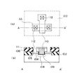
図1は、本発明の第1の実施形態に係る溝型チャネル構造のMOSトランジスタを示す図であり、図1(a)は平面図、図1(b)は同平面図のA−A’断面図、図1(b)は同平面図のB−B’断面図である。以下の実施形態では、nチャネルのMOSトランジスタについて説明するが、pチャネルのMOSトランジスタの場合には各導電型を逆にすれば良い。
【0046】
図中、101はp型のシリコン基板を示しており、このシリコン基板101の表面にはトレンチ型の素子分離絶縁膜102が形成されている。シリコン基板101上には層間絶縁膜106が形成されている。ここで、素子形成領域(AA:Active Area)のシリコン基板101の不純物濃度は、5×1015cm-3程度である。
【0047】
素子分離絶縁膜102で規定された素子形成領域の層間絶縁膜106からその下のシリコン基板101にかけては凹部107が形成されている。この凹部107は層間絶縁膜106を貫通し、シリコン基板101の途中の深さまで達している。
【0048】
凹部107内にはゲート絶縁膜109を介してゲート電極110が埋込み形成されている。ゲート絶縁膜109は例えば厚さ4.0nm程度の熱酸化膜である。
【0049】
ゲート絶縁膜109はシリコン基板101とゲート電極110との界面に形成されている。したがって、シリコン基板101内に埋め込まれた部分のゲート電極110の底面および側面はゲート絶縁膜109で覆われている。
【0050】
また、ゲート電極110は、例えばポリシリコン膜、またはTiN膜やRu膜等のメタル膜で構成されている。ゲート電極110のチャネル方向の幅は、例えば0.1〜0.15μm程度である。凹部107の底面下のチャネル領域には、しきい値電圧を調整するために、不純物濃度5×1017cm-3程度のチャネルイオン注入層108が形成されている。
【0051】
低不純物濃度のn型のソース・ドレイン拡散層104およびその上の高不純物濃度のn型のソース・ドレイン拡散層105は、ゲート電極110と自己整合的に形成されている。
【0052】
ここで、ソース・ドレイン拡散層104のシリコン基板101の表面からの拡散深さ、不純物濃度は、それぞれ0.2μm程度、5×1019cm-3程度である。一方、ソース・ドレイン拡散層105の拡散深さ、不純物濃度は、それぞれ0.15μm程度、5×1020cm-3程度である。
【0053】
層間絶縁膜106,111にはゲート電極110、ソース・ドレイン拡散層105に対してのコンタクトホール112が開孔されており、このコンタクトホール112を介して配線113がゲート電極110、n型ソース・ドレイン拡散層105にコンタクトしている。
【0054】
ここで、層間絶縁膜106,111は例えばSiO2 膜であり、配線113は例えばAl膜で形成されている。
【0055】
このように構成された溝型チャネル構造のMOSトランジスタによれば、層間絶縁膜106を貫通し、かつ素子形成領域のシリコン基板101の途中の深さまで達した凹部107内にゲート絶縁膜109を介してゲート電極110が埋め込まれ、かつ凹部107を挟むようにシリコン基板101の表面にソース・ドレイン拡散層104,105が形成されているので、ゲート電極110がソース・ドレイン拡散層104,105の上まで張り出すことはない。したがって、本実施形態によれば、溝型チャネル構造のMOSトランジスタの微細化を図れる。
【0056】
また、本実施形態によれば、ソース・ドレイン拡散層104,105の底面が凹部の底面のチャネルよりも上にあるので、ソース・ドレイン拡散層104,105の接合深さが実質的にマイナスになり、これにより微細化を進めてもショートチャネル効果を抑制できるようになる。
【0057】
また、ソース・ドレイン拡散層104,105の接合深さを実質的にマイナスに保ったままソース・ドレイン拡散層104,105の接合深さを深くすれば、ソース・ドレイン拡散層104,105の低抵抗化を図ることができる。
【0058】
また、ゲート電極110の抵抗を下げるためにゲート電極110の高さを増加させても、ゲート電極110の一部がシリコン基板101中に埋め込み形成されているため、ゲート電極110によって形成される段差を緩和できる。
【0059】
次に本実施形態の溝型チャネル構造のMOSトランジスタの製造方法について説明する。図2〜図7はその製造方法を示す工程図である。各図(a)は平面図、各図(b)は同平面図のA−A’断面図を示している。
【0060】
まず、図2に示すように、不純物濃度5×1015cm-3程度のp型のシリコン基板101を用意する。あるいはp型シリコン基板の表面に例えば厚さ1μm程度のpまたはn型シリコン層をエピタキシャル成長させてなる、いわゆるエピタキシャル基板を用いても良い。
【0061】
なお、同一基板にnチャネルおよびpチャネルのMOSトランジスタを形成するいわゆるCMOS構造の場合には、シリコン基板101の(100)面のnチャネルトランジスタ形成領域にはp型ウェルを形成し、pチャネルトランジスタ形成領域にはn型ウェルを形成する。以下では、nチャネルトランジスタの場合について説明する。pチャネルMOSトランジスタの場合には、不純物の型を逆に変えれ良い。
【0062】
次に同図に示すように、例えば反応性イオンエッチング(RIE)法を用いてシリコン基板101の表面に深さ約0.35μm程度のトレンチを掘り、そのトレンチ内にSiO2 膜などの素子分離絶縁膜102を埋め込むことにより、STI(Shallow Trench Isolation)と呼ばれる素子分離を行う。
【0063】
次に同図に示すように、厚さ8.0nm程度のSiO2 膜103を形成した後、このSiO2 膜103上に例えばフォトレジストパターン(図示せず)を形成し、これをマスクに用いて所望の領域にイオン注入を行うことにより、低不純物濃度のソース・ドレイン拡散層(LDD)となる低不純物濃度のn型拡散層104を形成する。イオン注入の条件は、例えばリン(P+ )のイオン注入であれば加速電圧70KeV程度、ドーズ量4×1013cm-2程度である。
【0064】
続いて同レジストパターンをマスクに用いてイオン注入を行うことにより、高不純物濃度のソース・ドレイン拡散層となる高不純物濃度のn型拡散層105を低不純物濃度のn型拡散層104の表面に形成する。イオン注入の条件は、例えば砒素(As)のイオン注入であれば、加速電圧30KeV程度、ドーズ量5×1015cm-2程度である。この後、マスクとして用いたフォトレジストパターンを剥離する。
【0065】
なお、本実施形態では、ドレイン基板の電界を緩和するためにLDD構造のソース・ドレイン拡散層を形成するが、低不純物濃度または高不純物濃度のソース・ドレイン拡散層のみのを形成しても良い(シングル・ソース・ドレイン方式)。
【0066】
次に同図に示すように、全面にSiO2 からなる厚さ200nm程度の層間絶縁膜106を例えばCVD法を用いて形成した後、例えば800℃程度のN2 雰囲気中で30分程度デンシファイを行う。
【0067】
この熱工程はn型拡散層104,105中の不純物の活性化も兼ねている。また、n型拡散層104,105の深さ(Xj)を抑えたいときは、デンシファイの温度を750℃程度に低温化して、950℃で10秒程度のRTA(Rapid Thermal Anneal)プロセスを併用してn型拡散層104,105中の不純物の活性化を行っても良い。
【0068】
次に図3に示すように、ゲート電極が形成される領域に、層間絶縁膜106を貫通し、シリコン基板101の途中の深さまで達した凹部107をレジスト(図示せず)をマスクにエッチングにより形成するとともに、凹部107によりn型拡散層104,105を2つに分離することによって、1対の低不純物濃度のソース・ドレイン拡散層(LDD)104およびその上に1対の高不純物濃度のソース・ドレイン拡散層105を形成する。
【0069】
具体的には、例えばフォトレジストパターン(図示せず)をマスクに用いて、ゲート電極が形成される領域のSiO2 膜103、層間絶縁膜106、シリコン基板101をRIE法にてエッチングすることにより、底面が基板表面から0.30μm程度の位置にある凹部107を形成する。
【0070】
その後、凹部107を形成する際のエッチング時に生じたエッチングポリマー層(図示せず)等を除去した後、シリコン基板101のシリコン表面を露出させ、例えば900℃の水素雰囲気中で3分程度熱処理を行うことにより、凹部107表面のSi原子を動かす。
【0071】
このとき、シリコン原子はシリコン表面積が最小になるように動くので、凹部107を形成する際のエッチング時に生じたダメージ等を回復させることができる。もちろん、これ以外のエッチング・ダメージ回復および除去の手段を用いても良い。
【0072】
次に同図に示すように、凹部107の底面の露出したシリコン表面に厚さ5nm程度のダミーSiO2 膜(図示せず)を例えば熱酸化法により形成した後、層間絶縁膜106等またはフォトレジスト(図示せず)をマスクに用いて、凹部107の底面下のシリコン基板101(チャネル領域)に対して選択的にチャネルイオン注入を行って、チャネルイオン注入層108を形成する。
【0073】
nチャネルトランジスタの場合、例えば0.7V程度のしきい値電圧(Vth)を設定するためには、例えば加速電圧10KeV、ドーズ量5×1012cm-2程度の条件でボロン(B+ )をイオン注入し、チャネル領域にp型のチャネルイオン注入層108を選択的に形成する。
【0074】
この工程は、図2の工程の段階でSiO2膜103を通して全面にイオン注入を行なうようにしても良いが、その場合には選択的なチャネルイオン注入を行うことができない。
【0075】
また、チャネルイオン注入層108中の不純物の活性化は、この後、例えばRTA(Rapid Thermal Anneal)を用いて800℃、10秒程度の熱処理で行っても良い。
【0076】
この後の熱工程を考慮して、トランジスタのショート・チャネル効果を抑制できるように、チャネル領域(チャネルイオン注入層108)の不純物プロファイルを最適化する。
【0077】
次に図4に示すように、ダミーSiO2膜(図示せず)を除去した後、熱酸化により基板表面の凹部107の内面(底面、側面)にゲート絶縁膜(熱酸化膜)109を形成する。また、酸化膜の表面を熱窒化した膜をゲート絶縁膜に用いても良い。さらに、CVD−SiO2 膜、CVD−SiON膜、またはCVD−Si3 N4 膜を含む積層膜をゲート絶縁膜に用いても良い。
【0078】
次に図5に示すように、凹部107の内部を充填するように、ゲート電極となる導電膜110を全面に形成する。導電膜110としては、例えば不純物を高濃度にドープしたポリシリコン膜やメタル膜を用いる。メタル膜としては、例えばRu膜、TiN膜、W膜、タングステンナイトライド膜(WNx )膜、WSi2 膜、TiSi2 膜またはこれらの積層膜があげられる。もちろん、CVD−SiO2 膜、CVD−SiON膜、CVD−Si3 N4 膜を含む積層膜をゲート絶縁膜に用いた場合には、不純物をドープしたポリシリコン膜をゲート電極として用いても良い。
【0079】
次に図6に示すように、凹部107の外部の導電膜110をCMP法により研磨除去することにより、凹部107の内部にゲート電極110を埋込み形成する。
【0080】
次に図7に示すように、全面にSiO2 膜からなる厚さ150nm程度の層間絶縁膜111を形成した後、ソース・ドレイン拡散105、ゲート電極110に対してのコンタクトホール112を層間絶縁膜106,111に開孔する。
【0081】
最後に、Al膜またはAl−Cu膜等のメタル膜を全面に形成し、このメタル膜をパターニングして、図1に示すように配線113を形成した後、パッシベーション膜(図示せず)を全面に形成して、トランジスタの基本構造が完了する。
【0082】
本実施形態の製造方法によれば、ソース・ドレイン拡散層104,105をゲート電極110と自己整合的に形成できるようになる。
【0083】
また、CMP法を用いてゲート電極110を埋込み形成しているので、RIE法を用いてゲート電極を埋込み形成する場合とは異なり、ゲート電極形成時のプラズマプロセスダメージ(例えばゲート絶縁膜109の絶縁破壊、ゲート絶縁膜109の信頼性低下)の問題はない。
【0084】
また、CMP法を用いてゲート電極110を埋込み形成しているので、RIE法を用いた場合とは異なり、メタルゲート電極を用いてもその材料の制約(例えばエッチング性についての制約)はない。
【0085】
また、チャネル領域に不純物イオンを選択的に注入することにより、チャネルイオン注入層108を形成できるので、つまりソース・ドレイン拡散層104,105にはよけいな不純物が導入されないので、ソース・ドレインの接合容量およびソース・ドレイン拡散層と基板間の逆方向PN接合リーク電流の増加を防止できる。
【0086】
また、チャネルイオン注入層108はソース・ドレイン拡散層104,105の活性化アニールの高温熱工程を受けないので、急峻な不純物プロファイルを維持でき、短チャネル効果を抑えるのに最適な不純物プロファイルを有するチャネルイオン注入層108を実現できる。
【0087】
また、ソース・ドレイン拡散層104を得るために、RIE法による側壁残し工程が不要になるので、工程が簡略化する。
【0088】
(第2の実施形態)
図8は、本発明の第2の実施形態に係る溝型チャネル構造のMOSトランジスタを示す断面図である。なお、図1と対応する部分には図1と同一符号を付してあり、詳細な説明は省略する(他の実施形態も同様)。
【0089】
本実施形態が第1の実施形態と主として異なる点は、熱酸化膜の代わりに堆積絶縁膜(例えばCVD絶縁膜)をゲート絶縁膜114に用いたことにある
本実施形態によれば、ゲート絶縁膜114として堆積絶縁膜を用いているので、熱酸化膜等に比べて、凹部内側に張り出して形成される。すなわち、リソグラフィの限界で決まる寸法よりもゲート絶縁膜114の膜厚の約2倍分だけ、チャネル長を短くできる。その結果、短チャネル化が実現され、これによりランジスタの性能をさらに向上させることができる。
【0090】
また、STI等の溝掘り型の素子分離を行った場合には、素子分離絶縁膜102と素子分離溝との境界部に微少な窪みが生じても、その窪みはゲート絶縁膜114(堆積絶縁膜)で埋め込まれる。
【0091】
これにより、いわゆるコーナーデバイス(寄生トランジスタ)の発生を防止でき、しきい値電圧の変動等の素子特性の劣化を防止できるようになる。また、溝型チャネル構造のMOSトランジスタを集積形成した場合には、MOSトランジスタ間のしきい値電圧等の素子特性のばらつきを抑制できるようになる。
【0092】
次に本実施形態の溝型チャネル構造のMOSトランジスタの製造方法について説明する。なお、ゲート絶縁膜114を形成する前までの工程(ダミーSiO2 膜を除去するまでの工程)は同じなので省略する。
【0093】
まず、CVD法等の堆積法を用いて堆積型のゲート絶縁膜114を全面に形成する。例えば、CVD法を用いて厚さ20nm程度の高誘電体膜(例えばTa2 O5 膜)をゲート絶縁膜114として形成する。
【0094】
このとき、凹部107のシリコン表面と高誘電体膜(ゲート絶縁膜114)との界面に、いわゆる界面準位等ができ難くするために、また、凹部107のシリコン表面と高誘電体膜との界面での反応を防止するためには以下のようにすれば良い。
【0095】
すなわち、凹部107のシリコン表面に薄い(例えば1nm程度)SiO2 膜を形成した後に高誘電体膜を形成したり、あるいはNH3 ガス雰囲気中でRTP(Rapid Thermal Process)により凹部107のシリコン表面に直接窒化した膜を形成した後に高誘電体膜を形成したり、あるいは厚さ1nm程度のSiO2 膜の表面をNO2 ガス等を用いて表面窒化した、いわゆるオキシナイトライド膜などを介して高誘電体膜(例えばTa2 O5 膜、(Ba,Sr)TiO3 膜)を形成すると良い。
【0096】
また、CVD−SiO2 膜や、CVD−SiON膜や、CVD−Si3 N4 膜を含む積層絶縁膜をゲート絶縁膜114に用いても同じような効果が得られる。すなわち、成膜後に、例えば1000℃、10秒程度のRTPによる熱処理を行ってデンシファイすると、凹部107のSi表面と積層絶縁膜(ゲート絶縁膜114)との界面の界面準位が減少したり、リーク電流が減少するなど絶縁膜としての絶縁特性が改善されたりする。
【0097】
次にゲート絶縁膜114を介して凹部107内にゲート電極110をCMP法を用いて埋込み形成する。このときは、ゲート電極110の幅は、ゲート絶縁膜114の膜厚の2倍分だけ細くなっている。すなわち、トランジスタのチャネル長がリソグラフィーで決まる寸法よりさらに細くすることができる。
【0098】
ゲート電極110としては、例えば不純物をドープしたポリシリコン膜や、メタル膜(例えばRu膜、TiN膜、W膜、タングステンナイトライド(WNx )膜、WSi2 膜、TiSi2 膜またはこれらの積層膜)があげられる。もちろん、CVD−SiO2 膜、CVD−SiON膜、CVD−Si3 N4 膜を含む積層膜をゲート絶縁膜に用いた場合には、不純物をドープしたポリシリコン膜をゲート電極として用いても良い。
【0099】
この後の工程は第1の実施形態と同じである。
【0100】
このような製造方法によれば、ソース・ドレイン拡散層104,105の活性化およびリフロー工程などの高温熱処理工程をゲート絶縁膜114の形成前に行うことができる。
【0101】
したがって、ゲート絶縁膜114およびゲート電極110としてそれぞれ高誘電体膜およびメタル膜を使用してもこれらの膜はソース・ドレイン拡散層の活性化や平坦化のための高温工程を受けることがないので、リーク電流増加などのゲート絶縁膜114の劣化を抑えることができる。ゲート絶縁膜114として高誘電体膜を用いれば、ゲート絶縁膜114の酸化膜換算膜厚を薄くできるので、トランジスタの素子特性の改善を図ることができるようになる。
【0102】
また、CMP法を用いてゲート電極110を埋込み形成しているので、RIE法を用いた場合とは異なり、メタルゲート電極の材料の制約(例えば耐熱性)が無くなるので、高誘電体膜のリーク電流が下げられるようなメタルゲート電極を用いることができるようになる。
【0103】
その他、第1の実施形態と同様な効果が得られる。
【0104】
(第3の実施形態)
図9は、本発明の第3の実施形態に係る溝型チャネル構造のMOSトランジスタを示す図であり、図9(a)は平面図、図9(b)は同平面図のA−A’断面図である。
【0105】
第1の実施形態では、コンタクトホール112内にAl等の金属からなる配線113を直接埋込み形成したが、コンタクトホール112の開孔径が小さくなるとAl膜がコンタクトホール112の中に入っていかないので、配線113の信頼性が低下する。
【0106】
そこで、本実施形態では、コンタクトホール112の内面を覆うように例えばTi膜/TiN膜を全面に形成し、続いてコンタクトホール112の内部を充填するようにW膜を全面に形成した後、コンタクトホール112の外部のTi膜/TiN膜およびW膜をCMP法等を用いて除去することにより、プラグ電極(コンタクトプラグ)115を埋込み形成する。この後、配線113を形成すれば、コンタクトホールのアスペクトが高くても配線113の信頼性は高くなる。
【0107】
(第4の実施形態)
図10は、本発明の第4の実施形態に係る溝型チャネル構造のMOSトランジスタを示す図であり、図10(a)は平面図、図10(b)は同平面図のA−A’断面図、図10(b)は同平面図のB−B‘断面図である。
【0108】
本実施形態が第1の実施形態と異なる点は、ゲート電極110が素子分離絶縁膜102よりも深くシリコン基板101内に形成されていることにある。言い換えれば凹部107の底が素子分離溝の底より下にある。例えば、凹部107の深さは0.4μm、素子分離溝の深さは0.25μmである。
【0109】
このような構成であれば、図10(c)に示すようにチャネル幅を3次元的に形成できるため、トランジスタの平面積を増加させずにチャネル幅を増加できる。したがって、微細化を図れるという効果を維持したままチャネル電流の増加を図ることができる。
【0110】
(第5の実施形態)
図11は、本発明の第5の実施形態に係る溝型チャネル構造のMOSトランジスタを示す図であり、図11(a)は平面図、図11(b)は同平面図のA−A’断面図、図11(b)は同平面図のB−B‘断面図である。
【0111】
第1の実施形態では、凹部107のシリコン表面のエッチングダメージを除去するために、特別な高温工程(例えば、凹部107のシリコン表面を露出させた後、例えば900℃の水素雰囲気で3分程度の熱処理)を行って、凹部107のシリコン表面のSi原子を動かした。
【0112】
このとき、シリコン原子は凹部107のシリコン表面の面積が最小になるように動くので、凹部107のシリコン表面のエッチングダメージ等を回復させることができるが、この熱処理条件を調整(例えば、凹部107のシリコン表面を露出させた後、950℃の水素雰囲気で5分程度の熱処理に変更)することによって凹部107の形状を変化させることができる。
【0113】
すなわち、図11(b)に示すように、凹部107の底部をなだらかな円弧状に変形させることができる。このような構造をとると、凹部107の底部(ゲート絶縁膜109が形成される領域)に鋭角な角部が無くなるので、ゲート絶縁膜109の耐圧の向上を図ることができるとともに、チャネル部をなだらかにできるために電子の移動度の劣化を抑制することができ、これによりトランジスタ特性の向上を図ることができるようになる。
【0114】
(第6の実施形態)
図12は、本発明の第6の実施形態に係る溝型チャネル構造のMOSトランジスタの製造方法を示す工程断面図である。
【0115】
本実施形態が第1の実施形態と異なる点は、図12(a)に示すように層間絶縁膜106をエッチングして溝を形成し、その溝の側壁にSiO2 膜からなるサイドウォール117を形成した後、図12(b)に示すように、層間絶縁膜106およびサイドウォール117をマスクにしてシリコン基板101をエッチングすることにより、凹部107を形成することにある。
【0116】
サイドウォール117は、全面に例えば厚さ20nm程度のSiO2 膜を堆積した後、このSiO2 膜をRIE法にて全面エッチングするという、いわゆる側壁残しにより形成する。
【0117】
このような形成方法によれば、凹部107のチャネル長方向の幅の寸法を、リソグラフィの限界で決まる寸法よりも小さくできる。したがって、ゲート長の短いゲート電極を実現できる
通常のトランジスタでは、ゲート長(チャネル長さ)を短くすると、ショートチャネル効果が起こり、しきい値電圧(Vth)が低下してリーク電流が増加するなどの問題が発生する。
【0118】
しかし、本実施形態は、第1の実施形態と同様に、ソース・ドレイン拡散層104,105の接合深さが実質的にマイナスになるなどの理由により、ショートチャネル効果を抑えることができる。
【0119】
したがって、本実施形態によれば、サイドウォール117を形成して、チャネル長を短くすることにより、トランジスタの特性を向上させることが可能となる。
【0120】
(第7の実施形態)
本実施形態は、ゲート電極の、半導体基板の表面から突出する上部の厚さと、溝に埋め込まれた下部の厚さを、最適なトランジスタの性能が得られるように規定した例である。
【0121】
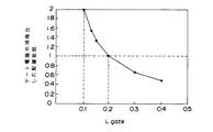
図14は、膜厚が一定(例えばH=0.10μm)でゲート長(L)が異なる3種類のゲート電極を示し、図15は、これらのゲート電極(タングステンからなる)のゲート長(Lgate)とゲート電極の配線抵抗との関係を示すグラフである。
【0122】
図15から、ゲート長(Lgate)が0.2μmから0.1μmに、1/2に短くなった場合、ゲート電極の配線抵抗は、約2倍となっていることがわかる。従って、ゲート電極の配線抵抗が素子性能(駆動速度等)に大きく影響する場合には、これまで、素子の微細化のためのLgateの短縮の要請に対して、ゲート電極の厚さを2倍にして素子性能の低下を防止していた。しかし、ゲート電極を厚くすると、ゲート電極が上方に突出し、段差が大きくなるため、平坦化のための層間絶縁膜を厚くしなければならず、そうすると層間絶縁膜に形成されるコンタクト孔のアスペクト比が大きくなり、コンタクトの形成が困難となるという問題があった。
【0123】
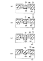
本実施形態に係るコンケーブ構造のトランジスタでは、ゲート電極の一部をSi基板中に埋め込むことにより、上記問題を解決しており、埋め込みの深さとして、次の3つの形がある。
【0124】
(1)トランジスタ特性を劣化させることなく、最適な深さにゲート電極70の一部がSi基板61中に埋め込まれている(図16(a))。
【0125】
(2)浅く埋め込まれている(図16(b))。
【0126】
(3)深く埋め込まれている(図16(c))。
【0127】
ここで、ゲート電極70のトータルの膜厚をH、ゲート電極70がSi基板61上に突出している寸法をh、ソース・ドレイン拡散領域の接合深さをXj、ゲート絶縁膜69の厚さをtOX、ソース・ドレイン拡散領域の底部のレベルとゲート電極70の下方のチャネル領域のレベルとの差をdとすると、図65A〜65Cから分かるように、以下の式(1)が成立する。
【0128】
H=h+Xj+d−tOX …(1)
本実施形態では、hとdの最適値について検討する。
【0129】
図17は、ゲート長Lgateとドレイン電流Idとの関係を示すグラフである。なお、ドレイン電流Idは、ゲート長Lgate=0.20μmの場合を1として規格化した値である。ここでは、Lgate=0.20μmのトランジスタとして、Xj、tOX等の値は、最適化されている。
【0130】
図17から、ゲート長Lgateが長くなるに従って、ドレイン電流Idは低下していることがわかる。ドレイン電流Idが20%以上低下すると、素子の動作に影響が生ずるので、ドレイン電流Idの20%の低下、即ちチャネル長L=0.25μm(Lgateの25%増)がチャネル長Lの上限であることがわかる。
【0131】
図16(a)〜(c)に示すようなコンケーブ構造のトランジスタの場合、ゲート電極70の埋め込みの深さが深ければ深いほど、トータルのチャネル長さ(l1 、l2 、l3 )は長くなる。これは、溝の側面もチャネル長に寄与するからである。
【0132】
これらの結果から、トランジスタの性能上、ゲート長Lgate(溝底部のチャネル長)およびdは、次の式を満たすことが望ましい。
【0133】
d<Lgate×0.25/2 …(2)
次に、図18を参照して、dの下限について検討する。
【0134】
ゲートがコンケーブ構造ではない平面構造のトランジスタの場合、ショートチャネル効果を防止するために、ソース・ドレイン拡散領域の接合深さXjを浅くすることが重要である。例えば、Xj=0.1μmのトランジスタに比べ、Xj=0.05μmのトランジスタの方がショートチャネル効果を低減出来ることが知られている。しかし、従来の平面構造のトランジスタでは、Xj=0μmとすることは原理的に不可能である。
【0135】
これに対し、本実施形態のようなコンケーブ構造のトランジスタでは、dの値を変えることにより、Xjを見掛上、マイナスにすることが可能である。このことは、コンケーブ構造のトランジスタにおいて、ショートチャネル効果を著しく低減できることを示している。即ち、図18に示すように、d=0(Xj=0に相当)からd=0.01μm、d=0.02μmと、dを増加させることにより、ショートチャネル効果を低減できることがわかる。従って、ショートチャネル効果を抑制するためには、d>0であることが重要である。なお、d>0.02μmでは、ショートチャネル効果の抑制効果は飽和している。
【0136】
次に、ゲート電極のSi基板上に突出している部分の高さhについて考える。図19は、hがh1 の場合、図20は、hがh1 より大きいh2 である場合をそれぞれ示す。L=0.20μmの場合を例にとって、L=0.20μmの設計ルールに従って、コンタクト孔80のアスペクト比(図中のh/Wに相当)を計算すると、図21に示すようになる。
【0137】
図19において、h1 =0.20μmの場合、コンタクト孔80のアスペクト比は1である。しかし、図21において、h2 =0.6μmの場合、コンタクト孔80のアスペクト比は3にもなる。このように大きなアスペクト比では、コンタクト孔80の形成およびコンタクトプラグの埋め込みが困難となるばかりか、コンタクトプラグの抵抗も増加してしまう。
【0138】
しかし、hが大きければ大きいほど、ゲート電極70の配線抵抗を低下させることが出来る。このことから、hは、トランジスタ特性において、ゲート電極の配線抵抗の低下と、コンタクトプラグの抵抗増加および埋め込み困難性とのトレードオフによって決定される値であることがわかる。
【0139】
従来のコンタクト形成の例およびトランジスタの特性の点から、コンタクト孔のアスペクト比は3以下にすることが望ましいことがわかっている。従って、ゲート電極の配線抵抗を考慮して、最低膜厚がゲート長Lより大きいことにすると、ゲート長Lを最小の設計寸法(デザインルール)として、次の式が成立する。
【0140】
Lgate<h<ゲート長L×3 …(3)
以上の関係をまとめると、以下のようになる。
【0141】
L+Xj−tOX<H<3×Lgate
L+Xj−tOX<H<3.125×Lgate+Xj−tOX …(4)
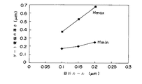
各デザインルール(L=0.20μm,0.15μm,0.10μm)におけるXj、dmax 、hmax 、tOX、Hmin 、Hmax の値は、以下の表のようになる。
【0142】
【表1】

(注)ソース/ドレイン領域の抵抗を下げるために、Xjは、一定値0.10μmとした。
【0144】
Hmin とHmax とをまとめたのが、図22である。図22に示すように、Hmin とHmax との間に入るように、各設計ルールにおいてゲート電極の厚みを調整することが必要である。
【0145】
図23(a)〜(c)は、ゲート電極70の厚みおよびSi基板61内に埋め込まれた部分の深さを種々変化させたトランジスタを示す。以上のことを考慮すると、図23(a)に示すように、Si基板61内に埋め込まれた部分の深さが浅過ぎると、ショートチャネル効果を抑制することが困難であり、図23(c)に示すように、Si基板61内に埋め込まれた部分の深さが深過ぎると、トランジスタのドレイン電流が低下し、図23(d)に示すように、ゲート電極70の厚みが薄いと、ゲート電極70の配線抵抗が大きくなってしまう。従って、図23(b)に示すような構造が最適である。
【0146】
図23(b)に示すような構造とすることにより、ゲート電極70の配線抵抗の増大による素子特性の劣化、コンタクト孔のアスペクト比の増大によるコンタクトの形成の困難さ、およびコンタクト抵抗の増大による素子特性の劣化を防止することが出来る。
【0147】
なお、本発明は、上記実施形態に限定されるものではない。例えば、上記実施形態では、ゲート絶縁膜の膜厚に関して、詳述しなかったが、例えば3.3V系と2.5V系などのように異なる複数の電圧に対応するために、ゲート絶縁膜の膜厚が異なる複数種のMOSトランジスタを形成しても良い。
【0148】
このようにするには、例えばゲート電極の工程前に、所望の膜厚のゲート絶縁膜を形成するトランジスタ領域外をマスクで覆って上記所望のトランジスタ領域に所望のゲート絶縁膜を選択的に形成する工程を繰り返せば良い。
【0149】
あるいは、所望の膜厚のゲート絶縁膜およびゲート電極を全てのトランジスタ領域に形成した後、上記所望の膜厚のゲート絶縁膜を形成するべきトランジスタ領域をマスクで覆って他のトランジスタ領域のゲート絶縁膜およびゲート電極を除去する工程を繰り返しても良い。
【0150】
このように同一チップ内にゲート絶縁膜の膜厚が異なる複数種のMOSトランジスタを形成すれば、例えばpチャネルMOSトランジスタおよびnチャネルMOSトランジスタのパフォーマンスをそれぞれ最大にできたり、あるいはメモリセル部のMOSトランジスタおよび周辺回路制御部のMOSトランジスタのパフォーマンスをそれぞれ最大にできる。
【0151】
また、ゲート絶縁膜の材料が異なる複数種のMOSトランジスタを形成しても良い。
【0152】
このようにするには、例えばまず第1のゲート絶縁膜(例えばSiO2 膜とその上に形成されたTa2 O5 膜との積層絶縁膜)を形成した後、この第1のゲート絶縁膜上にゲート電極(例えばRu膜)を全てのトランジスタ領域に形成する。
【0153】
次に、第2のゲート絶縁膜(例えばPZT膜等の強誘電体膜)を形成したい領域のトランジスタ領域の第1のゲート絶縁膜および第1のゲート電極を選択的に除去した後、そのトランジスタ領域に第2のゲート絶縁膜および第1のゲート電極を選択的に形成する。このとき、必要であれば、第1のゲート電極と材料が異なる第2のゲート電極を第2のゲート絶縁膜上に形成しても良い。以上の工程を必要な数だけ繰り返す。
【0154】
このように同一チップ内にゲート絶縁膜の材料が異なる複数種のMOSトランジスタを形成すれば、例えばpチャネルMOSトランジスタおよびnチャネルMOSトランジスタのパフォーマンスをそれぞれ最大にできたり、あるいはメモリセル部のMOSトランジスタおよび周辺回路制御部のMOSトランジスタのパフォーマンスをそれぞれ最大にできる。
【0155】
また、強誘電体膜をゲート絶縁膜に用いた強誘電体メモリ素子と高誘電体膜をゲート絶縁膜に用いたトランジスタを同じトランジスタ構造で一連のプロセスで連続して形成でき、これにより高集積メモリチップを簡単なプロセス工程実現できるようになる。
【0156】
その他、本発明の要旨を逸脱しない範囲で、種々変形して実施できる。
【0157】
【発明の効果】
以上説明したように、本発明によれば、層間絶縁膜を貫通し、かつ素子形成領域の半導体基板の途中の深さまで達した凹部内にゲート電極を埋め込み、かつ上記凹部を挟むように半導体基板の表面にソース・ドレイン拡散層を形成することにより、ゲート電極のソース・ドレイン拡散層上への張り出しを無くすことができるので、溝型チャネル構造のMOSトランジスタの微細化を図れる半導体装置およびその製造方法を実現できるようになる。
【0158】
また、ゲート電極の一部が基板中に埋め込まれているので、ゲート電極の抵抗を下げるためにゲート電極の膜厚が厚くしても、ゲート電極による段差を緩和することが出来る。
【0159】
更に、ゲート電極の基板中に埋め込まれている部分の寸法と基板の表面から突出している部分の寸法とを所定の範囲に規定することにより、最適な性能を有する半導体素子を得ることが可能である。
【図面の簡単な説明】
【図1】本発明の第1の実施形態に係る溝型チャネル構造のMOSトランジスタを示す平面図および断面図
【図2】本発明の第1の実施形態に係る溝型チャネル構造のMOSトランジスタの製造方法を示す平面図および断面図
【図3】本発明の第1の実施形態に係る溝型チャネル構造のMOSトランジスタの製造方法を示す平面図および断面図
【図4】本発明の第1の実施形態に係る溝型チャネル構造のMOSトランジスタの製造方法を示す平面図および断面図
【図5】本発明の第1の実施形態に係る溝型チャネル構造のMOSトランジスタの製造方法を示す平面図および断面図
【図6】本発明の第1の実施形態に係る溝型チャネル構造のMOSトランジスタの製造方法を示す平面図および断面図
【図7】本発明の第1の実施形態に係る溝型チャネル構造のMOSトランジスタの製造方法を示す平面図および断面図
【図8】本発明の第2の実施形態に係る溝型チャネル構造のMOSトランジスタを示す断面図
【図9】本発明の第3の実施形態に係る溝型チャネル構造のMOSトランジスタを示す平面図および断面図
【図10】本発明の第4の実施形態に係る溝型チャネル構造のMOSトランジスタを示す平面図および断面図
【図11】本発明の第5の実施形態に係る溝型チャネル構造のMOSトランジスタを示す平面図および断面図
【図12】本発明の第6の実施形態に係る溝型チャネル構造のMOSトランジスタを示す工程断面図
【図13】従来の溝型チャネル構造のMOSトランジスタを示す断面図
【図14】本発明の第7の実施形態における膜厚が一定でゲート長が異なる3種類のゲート電極を示す斜視図
【図15】本発明の第7の実施形態におけるゲート電極のゲート長(Lgate)とゲート電極の配線抵抗との関係を示す特性図
【図16】本発明の第7の実施形態におけるゲート電極のSi基板内に埋め込まれた深さが異なるトランジスタを示す断面図
【図17】本発明の第7の実施形態におけるゲート長Lgateとドレイン電流Idとの関係を示す特性図
【図18】本発明の第7の実施形態におけるゲート長Lgateとしきい値電圧との関係を示す特性図
【図19】本発明の第7の実施形態におけるゲート電極のSi基板上に突出している部分の高さが異なるトランジスタを示す断面図
【図20】本発明の第7の実施形態におけるゲート電極のSi基板上に突出している部分の高さが異なるトランジスタを示す断面図
【図21】本発明の第7の実施形態におけるゲート電極のSi基板上に突出している部分の高さとコンタクト孔のアスペクト比との関係を示す特性図
【図22】各デザインルールにおけるHmin とHmax を示す特性図
【図23】ゲート電極の厚みおよびSi基板内に埋め込まれた部分の深さを種々変化させたトランジスタを示す断面図。
【符号の説明】
61,101…シリコン基板
66,107,111…層間絶縁膜
69,109,114…ゲート絶縁膜
70,110…ゲート電極
80,112…コンタクトホール
73,113…配線
102…素子分離絶縁膜
103…SiO2 膜
104…ソース・ドレイン拡散層
105…ソース・ドレイン拡散層(LDD)
106…層間絶縁膜
107…凹部
108…チャネルイオン注入層
115…プラグ電極
117…サイドウォール[0001]
BACKGROUND OF THE INVENTION
The present invention relates to a semiconductor device having a MOS transistor having a so-called trench channel structure in which a part of a gate electrode is embedded in a substrate, and a method for manufacturing the same.
[0002]
[Prior art]
Silicon oxide film (SiO2In a MOS transistor using a film) as a gate oxide film, the thinning of the gate oxide film plays an important role in promoting the suppression of the short channel effect of the transistor. However, making the gate oxide film thinner than the film thickness at which direct tunneling occurs (for example, a film thickness thinner than about 3 nm) is considered to be a problem in transistor reliability.
[0003]
Further, in the conventional polycide gate structure (laminated structure of a polysilicon film and a silicide film), the gate electrode film thickness increases as the gate electrode width becomes finer, and the step difference of the gate electrode increases. Yes.
[0004]
Therefore, a metal gate electrode is adopted as a solution to these problems, or Ta2OFiveA method has been proposed in which a high dielectric film such as a film is used as a gate insulating film to reduce the equivalent oxide film thickness while suppressing leakage current (direct tunneling).
[0005]
However, the metal gate electrode has a problem in terms of heat resistance. On the other hand, a MOS transistor using a high dielectric film as a gate insulating film has the following problems.
[0006]
After the formation of the gate insulating film (high dielectric film), a high temperature thermal process (for example, formation of source / drain diffusion layers, reflow of the interlayer insulating film, etc.) ranging from 800 ° C. to 1000 ° C. is performed. An interface reaction between the films or an interface reaction between the gate insulating film and the gate electrode occurs.
[0007]
However, it is difficult for the gate insulating film (high dielectric film) to withstand such a high temperature process. As a result, the gate insulating film deteriorates, and there is a problem that it is difficult to obtain a MOS transistor having excellent electrical characteristics.
[0008]
As another solution, a MOS transistor having a groove-type channel structure (for example, Nishimatsu et al., Groove Gate MOSFET, 8th Conf. On Solid State Device, pp. 179-183, 1976) has been proposed.
[0009]
FIG. 13 shows a cross-sectional view of a conventional MOS transistor having a trench channel structure. In the figure, 201 is a p-type silicon substrate, 202 is an element isolation insulating film (STI), 203 is a gate insulating film, 204 is an LDD, 205 is a high impurity concentration source / drain diffusion layer, 206 is an interlayer insulating film, 207 is A gate electrode (polysilicon film) 208 is a source / drain wiring electrode.
[0010]
In this type of trench-type channel structure MOS transistor, since the gate electrode 207 extends over the source / drain diffusion layer 205, for example, a short circuit between the gate electrode 207 and the source / drain wiring electrode 208 due to misalignment is prevented. There is a need.
[0011]
For this purpose, the distance between the gate electrode 207 and the source / drain wiring electrode 208 may be increased, but this time there is a problem that it is difficult to miniaturize the element.
[0012]
Further, since the silicon surface of the recess formed by etching the silicon substrate 201 is used for the channel, it is required to remove the etching damage. However, since it is difficult to remove etching damage, there has been a problem that the characteristics of the element are not improved.
[0013]
[Problems to be solved by the invention]
As described above, in the conventional MOS transistor having the groove-type channel structure, the gate electrode extends over the source / drain diffusion layer, and therefore it is necessary to increase the distance between the gate electrode and the source / drain wiring electrode. There has been a problem that miniaturization of the element becomes difficult.
[0014]
In addition, in a conventional gate structure made of polycide (a laminated film of a polysilicon film and a silicide film), the gate electrode thickness is reduced in order to reduce the wiring resistance of the gate electrode as the width of the gate electrode is reduced. It was thick. For this reason, as the dimension of the gate electrode in the channel length (L) direction becomes smaller, the step difference of the gate electrode increases. Therefore, when forming a contact with the gate electrode, the aspect ratio of the contact hole is increased, which is problematic. It was.
[0015]
The present invention has been made in view of the above circumstances, and an object of the present invention is to provide a semiconductor device and a method for manufacturing the same that enable miniaturization of elements.
[0016]
Another object of the present invention is to provide a semiconductor device in which the resistance of the gate electrode is lowered and the level difference caused by the gate electrode is reduced, and a method for manufacturing the same.
[0017]
[Means for Solving the Problems]
In order to solve the above problems, the present invention provides a semiconductor substrate, a gate insulating film formed on a bottom surface and a side surface of a groove formed in the semiconductor substrate, and a trench in which a gate insulating film is formed on the bottom surface and the side surface. A gate electrode projecting from the surface of the semiconductor substrate, and a source region and a drain region formed in the surface region of the semiconductor substrate so as to sandwich the gate electrode,The channel length of the channel region formed along the trench is L, and the thickness of the gate insulating film is t OX , The thickness of the gate electrode is H, and the length of the gate electrode is L gate When the junction depth of the source / drain diffusion layer is Xj, the following equation is satisfied:A semiconductor device is provided.
[0019]
L + Xj-tOX<H <3.125 × Lgate+ Xj-tOX
In such a semiconductor device, the gate insulating film can be a deposited insulating film.
[0020]
The gate electrode can be formed in the semiconductor substrate deeper than the element isolation insulating film.
[0021]
Furthermore, the bottom of the groove in the semiconductor substrate can be formed with roundness.
[0023]
The present invention also includes a step of forming a diffusion layer to be a pair of source / drain diffusion layers on the surface of a semiconductor substrate, a step of forming an interlayer insulating film on the semiconductor substrate, the interlayer insulating film and the semiconductor Forming a groove by selectively removing the substrate and separating the diffusion layer into two by the groove; and forming a gate insulating film on the bottom and side surfaces of the groove Forming a gate electrode so that a lower portion is embedded in a groove in which a gate insulating film is formed on the bottom surface and side surfaces, and an upper portion protrudes from the surface of the semiconductor substrate, and The channel length of the channel region formed along the groove is L, and the thickness of the gate insulating film is t.OX, The thickness of the gate electrode is H, and the length of the gate electrode is Lgate , The junction depth of the source / drain diffusion layer is XjThen, the manufacturing method of the semiconductor device characterized by satisfying the following formula is provided.
[0024]
L + Xj-tOX<H <3.125 × Lgate+ Xj-tOX
In these semiconductor device manufacturing methods, after the formation of the source / drain diffusion layers, a conductive film is formed on the entire surface so as to fill the groove, and then the conductive film outside the groove is formed by CMP. By polishing and removing, the gate electrode made of the conductive film can be embedded.
[0025]
A more specific configuration of the present invention is as follows.
[0026]
(1) The gate insulating film is Ta2OFiveSingle layer film, or Ta2OFiveIt is a laminated film including a film.
[0027]
(2) The gate insulating film is a single layer film containing Ba, Sr and Ti, or a laminated film containing Ba, Sr and Ti.
[0028]
(3) The gate electrode is a metal gate electrode.
[0029]
(4) Gate insulating films having different film thicknesses are used in the same chip.
[0030]
(5) Gate insulating films made of different materials are used in the same chip.
[0031]
(6) In the present invention, (4) or (5), there are a region where a ferroelectric film is used as a gate insulating film and a region where a high dielectric film is used as a gate insulating film.
[0032]
(7) The gate electrode is a polycrystalline silicon film doped with impurities.
[0033]
(8) After forming a diffusion layer (LDD) having a low impurity concentration, a diffusion layer (source / drain) having a high impurity concentration is formed on the surface of the diffusion layer, thereby forming a source / drain diffusion layer having an LDD structure. Form.
[0034]
As described above, according to the semiconductor device of the present invention, since a part of the gate electrode is embedded in the substrate, the gate electrode can be increased even if the gate electrode is thickened to reduce the resistance of the gate electrode. Steps due to the electrodes can be reduced.
[0035]
In addition, it is possible to obtain a semiconductor device having optimum performance by defining the dimension of the portion embedded in the substrate of the gate electrode and the dimension of the portion protruding from the surface of the substrate within a predetermined range. is there.
[0036]
In particular, by using a deposited insulating film (for example, a CVD insulating film) as the gate insulating film, the film is formed so as to protrude to the inside of the recess compared to a thermal oxide film or the like. That is, the channel length can be shortened by about twice the thickness of the deposited insulating film than the dimension determined by the limit of lithography. As a result, a short channel can be realized, which can improve the performance of the transistor.
[0037]
In addition, when trench-type element isolation such as STI is performed, even if a minute recess is formed at the boundary between the element isolation insulating film and the element isolation trench, the recess is a gate insulating film (deposited insulating film). Embedded in. As a result, the generation of so-called corner devices (parasitic transistors) can be prevented, and deterioration of element characteristics can be prevented.
[0038]
Further, by forming the gate electrode deeper than the element isolation insulating film in the semiconductor substrate, the channel width can be increased without increasing the planar area of the transistor. Therefore, it is possible to increase the channel current while maintaining the effect of miniaturization.
[0039]
Furthermore, by forming the bottom of the groove with a round shape, sharp corners are eliminated, so that the breakdown voltage of the gate insulating film is improved, and the transistor characteristics are improved such as the channel is rounded and the channel current is increased. Can do.
[0040]
Furthermore, by making the bottom surface of the source / drain diffusion layer above the bottom surface of the groove, the junction depth of the source / drain diffusion layer becomes substantially negative, and even if miniaturization is promoted. Short channel effect can be suppressed.
[0041]
Further, according to the method for manufacturing a semiconductor device of the present invention, the source / drain diffusion layer of the MOS transistor having the groove type channel structure according to the present invention can be formed in self-alignment with the gate electrode.
[0042]
In addition, since the gate insulating film can be formed after a high temperature heat treatment process (for example, a source / drain diffusion layer activation process, a metal gate electrode formation process, a gate electrode post-oxidation process, a reflow process), An insulating film that is easily deteriorated by heat, such as a dielectric film or a high dielectric film, can be used. Thus, for example, by using a ferroelectric film, the equivalent oxide thickness of the gate insulating film can be reduced, and the device characteristics of the transistor can be improved.
[0043]
In particular, by embedding the gate electrode using the CMP method, unlike the case of embedding the gate electrode using the RIE method, plasma process damage during the formation of the gate electrode (for example, dielectric breakdown of the gate insulating film) ) There is no problem. Further, unlike the case where the CMP method is used, there are no restrictions on the material of the metal electrode (for example, heat resistance).
[0044]
DETAILED DESCRIPTION OF THE INVENTION
Hereinafter, embodiments of the present invention (hereinafter, embodiments) will be described with reference to the drawings.
[0045]
(First embodiment)
1A and 1B show a MOS transistor having a trench channel structure according to a first embodiment of the present invention. FIG. 1A is a plan view and FIG. 1B is an AA ′ view of the same plan view. Sectional drawing and FIG.1 (b) are BB 'sectional drawing of the same top view. In the following embodiments, an n-channel MOS transistor will be described. However, in the case of a p-channel MOS transistor, each conductivity type may be reversed.
[0046]
In the figure,
[0047]
A
[0048]
A
[0049]
The
[0050]
The
[0051]
The low impurity concentration n-type source /
[0052]
Here, the diffusion depth and impurity concentration of the source /
[0053]
Contact holes 112 for the
[0054]
Here, the
[0055]
According to the MOS transistor having the groove-type channel structure configured as described above, the
[0056]
Further, according to the present embodiment, since the bottom surfaces of the source / drain diffusion layers 104 and 105 are above the channel at the bottom surface of the recess, the junction depth of the source / drain diffusion layers 104 and 105 is substantially negative. Thus, the short channel effect can be suppressed even if miniaturization is advanced.
[0057]
Further, if the junction depth of the source / drain diffusion layers 104, 105 is increased while the junction depth of the source / drain diffusion layers 104, 105 is kept substantially negative, the lower of the source / drain diffusion layers 104, 105 is achieved. Resistance can be achieved.
[0058]
Even if the height of the
[0059]
Next, a method for manufacturing the MOS transistor having the trench channel structure according to this embodiment will be described. 2 to 7 are process diagrams showing the manufacturing method. Each drawing (a) is a plan view, and each drawing (b) is a cross-sectional view taken along the line A-A 'of the plan view.
[0060]
First, as shown in FIG. 2, the impurity concentration is 5 × 10.15cm-3A p-
[0061]
In the case of a so-called CMOS structure in which n-channel and p-channel MOS transistors are formed on the same substrate, a p-type well is formed in the n-channel transistor formation region on the (100) plane of the
[0062]
Next, as shown in the figure, for example, a reactive ion etching (RIE) method is used to dig a trench having a depth of about 0.35 μm on the surface of the
[0063]
Next, as shown in the figure, SiO having a thickness of about 8.0 nm.2After forming the
[0064]
Subsequently, by performing ion implantation using the resist pattern as a mask, the n-
[0065]
In this embodiment, the source / drain diffusion layer having the LDD structure is formed in order to relax the electric field of the drain substrate. However, only the source / drain diffusion layer having a low impurity concentration or a high impurity concentration may be formed. (Single source drain method).
[0066]
Next, as shown in FIG.2After the
[0067]
This thermal process also serves to activate the impurities in the n-type diffusion layers 104 and 105. In addition, when it is desired to suppress the depth (Xj) of the n-type diffusion layers 104 and 105, the densify temperature is lowered to about 750 ° C., and an RTA (Rapid Thermal Annealing) process at 950 ° C. for about 10 seconds is used together. Then, the impurities in the n-type diffusion layers 104 and 105 may be activated.
[0068]
Next, as shown in FIG. 3, a
[0069]
Specifically, for example, using a photoresist pattern (not shown) as a mask, SiO in the region where the gate electrode is to be formed2The
[0070]
Thereafter, after removing the etching polymer layer (not shown) and the like generated during the etching for forming the
[0071]
At this time, since the silicon atoms move so as to minimize the silicon surface area, it is possible to recover damage or the like caused during etching when the
[0072]
Next, as shown in the figure, a dummy SiO having a thickness of about 5 nm is formed on the exposed silicon surface of the bottom surface of the recess 107.2After a film (not shown) is formed by, for example, a thermal oxidation method, the
[0073]
In the case of an n-channel transistor, for example, in order to set a threshold voltage (Vth) of about 0.7 V, for example, an acceleration voltage of 10 KeV and a dose amount of 5 × 1012cm-2Boron (B+) Is ion-implanted to selectively form a p-type channel ion-implanted
[0074]
This process is performed at the stage of the process shown in FIG.2Although ion implantation may be performed on the entire surface through the
[0075]
Further, the activation of the impurities in the channel
[0076]
In consideration of the subsequent thermal process, the impurity profile of the channel region (channel ion implantation layer 108) is optimized so that the short channel effect of the transistor can be suppressed.
[0077]
Next, as shown in FIG.2After removing the film (not shown), a gate insulating film (thermal oxide film) 109 is formed on the inner surface (bottom surface, side surface) of the
[0078]
Next, as shown in FIG. 5, a
[0079]
Next, as shown in FIG. 6, the
[0080]
Next, as shown in FIG.2After the
[0081]
Finally, a metal film such as an Al film or an Al—Cu film is formed on the entire surface, and this metal film is patterned to form a
[0082]
According to the manufacturing method of this embodiment, the source / drain diffusion layers 104 and 105 can be formed in self-alignment with the
[0083]
In addition, since the
[0084]
In addition, since the
[0085]
In addition, since channel ions implanted
[0086]
Further, since the channel
[0087]
In addition, in order to obtain the source /
[0088]
(Second Embodiment)
FIG. 8 is a sectional view showing a MOS transistor having a trench channel structure according to the second embodiment of the present invention. 1 corresponding to those in FIG. 1 are denoted by the same reference numerals as those in FIG. 1, and detailed description thereof is omitted (the same applies to other embodiments).
[0089]
This embodiment is mainly different from the first embodiment in that a deposited insulating film (for example, a CVD insulating film) is used for the
According to the present embodiment, since the deposited insulating film is used as the
[0090]
In addition, when trench-type element isolation such as STI is performed, even if a minute dent is generated at the boundary between the element
[0091]
As a result, the generation of so-called corner devices (parasitic transistors) can be prevented, and deterioration of element characteristics such as threshold voltage fluctuations can be prevented. In addition, when MOS transistors having a groove-type channel structure are formed in an integrated manner, variations in element characteristics such as threshold voltage between the MOS transistors can be suppressed.
[0092]
Next, a method for manufacturing the MOS transistor having the trench channel structure according to this embodiment will be described. Note that the steps up to the formation of the gate insulating film 114 (
[0093]
First, a deposition type
[0094]
At this time, in order to make it difficult to form a so-called interface state at the interface between the silicon surface of the
[0095]
That is, thin (for example, about 1 nm) SiO on the silicon surface of the recess 107.2After the film is formed, a high dielectric film is formed, or NHThreeAfter forming a film directly nitrided on the silicon surface of the
[0096]
CVD-SiO2Film, CVD-SiON film, CVD-SiThreeNFourThe same effect can be obtained even when a stacked insulating film including a film is used for the
[0097]
Next, the
[0098]
Examples of the
[0099]
The subsequent steps are the same as those in the first embodiment.
[0100]
According to such a manufacturing method, high-temperature heat treatment steps such as activation and reflow steps of the source / drain diffusion layers 104 and 105 can be performed before the
[0101]
Therefore, even if a high dielectric film and a metal film are used as the
[0102]
In addition, since the
[0103]
In addition, the same effects as those of the first embodiment can be obtained.
[0104]
(Third embodiment)
FIGS. 9A and 9B are views showing a MOS transistor having a trench channel structure according to the third embodiment of the present invention. FIG. 9A is a plan view, and FIG. 9B is an AA ′ view of the plan view. It is sectional drawing.
[0105]
In the first embodiment, the
[0106]
Therefore, in this embodiment, for example, a Ti film / TiN film is formed on the entire surface so as to cover the inner surface of the
[0107]
(Fourth embodiment)
10A and 10B are views showing a groove type channel structure MOS transistor according to a fourth embodiment of the present invention, in which FIG. 10A is a plan view and FIG. 10B is an AA ′ view of the same plan view. Sectional drawing and FIG.10 (b) are BB 'sectional drawing of the same top view.
[0108]
The present embodiment is different from the first embodiment in that the
[0109]
With such a configuration, the channel width can be three-dimensionally formed as shown in FIG. 10C, so that the channel width can be increased without increasing the planar area of the transistor. Therefore, it is possible to increase the channel current while maintaining the effect of miniaturization.
[0110]
(Fifth embodiment)
FIGS. 11A and 11B are views showing a MOS transistor having a groove-type channel structure according to the fifth embodiment of the present invention. FIG. 11A is a plan view and FIG. 11B is an AA ′ view of the plan view. Sectional drawing and FIG.11 (b) are BB 'sectional drawing of the same top view.
[0111]
In the first embodiment, in order to remove etching damage on the silicon surface of the
[0112]
At this time, since the silicon atoms move so that the area of the silicon surface of the
[0113]
That is, as shown in FIG. 11B, the bottom of the
[0114]
(Sixth embodiment)
FIG. 12 is a process cross-sectional view illustrating a method for manufacturing a MOS transistor having a trench channel structure according to a sixth embodiment of the present invention.
[0115]
The present embodiment is different from the first embodiment in that a groove is formed by etching the
[0116]
The
[0117]
According to such a formation method, the width dimension of the
In a normal transistor, when the gate length (channel length) is shortened, a short channel effect occurs, causing problems such as a decrease in threshold voltage (Vth) and an increase in leakage current.
[0118]
However, the present embodiment can suppress the short channel effect because the junction depth of the source / drain diffusion layers 104 and 105 is substantially negative, as in the first embodiment.
[0119]
Therefore, according to the present embodiment, the characteristics of the transistor can be improved by forming the
[0120]
(Seventh embodiment)
The present embodiment is an example in which the thickness of the upper part of the gate electrode protruding from the surface of the semiconductor substrate and the thickness of the lower part embedded in the groove are defined so as to obtain optimum transistor performance.
[0121]
FIG. 14 shows three types of gate electrodes having a constant film thickness (for example, H = 0.10 μm) and different gate lengths (L). FIG. 15 shows the gate lengths (L) of these gate electrodes (made of tungsten).gate) And the wiring resistance of the gate electrode.
[0122]
From FIG. 15, the gate length (Lgate) Decreases from 0.2 μm to 0.1 μm to ½, it can be seen that the wiring resistance of the gate electrode is approximately doubled. Therefore, when the wiring resistance of the gate electrode greatly affects the element performance (driving speed, etc.), LgateTherefore, the gate electrode thickness is doubled to prevent the device performance from decreasing. However, when the gate electrode is made thicker, the gate electrode protrudes upward and the step becomes larger, so the interlayer insulating film for planarization must be made thicker. Then, the aspect ratio of the contact hole formed in the interlayer insulating film There is a problem that it becomes difficult to form a contact.
[0123]
The concave structure transistor according to the present embodiment solves the above problem by embedding a part of the gate electrode in the Si substrate, and there are the following three types of embedding depth.
[0124]
(1) A part of the
[0125]
(2) It is buried shallowly (FIG. 16B).
[0126]
(3) It is embedded deeply (FIG. 16C).
[0127]
Here, the total film thickness of the
[0128]
H = h + Xj + dtOX ... (1)
In this embodiment, the optimum values of h and d are examined.
[0129]
FIG. 17 shows the gate length LgateAnd a drain current Id. The drain current Id is the gate length Lgate= 0.20 μm is standardized as 1. Here, Lgate= 0.20 μm, Xj, tOXThe values such as are optimized.
[0130]
From FIG. 17, the gate length LgateIt can be seen that the drain current Id decreases as the length increases. If the drain current Id decreases by 20% or more, the operation of the device is affected. Therefore, the drain current Id decreases by 20%, that is, the channel length L = 0.25 μm (Lgate(25% increase) is the upper limit of the channel length L.
[0131]
In the case of a transistor having a concave structure as shown in FIGS. 16A to 16C, the deeper the buried depth of the
[0132]
From these results, the gate length L is considered in terms of transistor performance.gateIt is desirable that (the channel length of the groove bottom) and d satisfy the following formula.
[0133]
d <Lgate× 0.25 / 2 (2)
Next, the lower limit of d will be examined with reference to FIG.
[0134]
In the case of a planar transistor whose gate is not a concave structure, it is important to reduce the junction depth Xj of the source / drain diffusion region in order to prevent the short channel effect. For example, it is known that the transistor with Xj = 0.05 μm can reduce the short channel effect compared to the transistor with Xj = 0.1 μm. However, in the conventional planar structure transistor, it is impossible in principle to set Xj = 0 μm.
[0135]
On the other hand, in a transistor having a concave structure as in this embodiment, it is possible to make Xj apparently negative by changing the value of d. This indicates that the short channel effect can be remarkably reduced in a transistor having a concave structure. That is, as shown in FIG. 18, it is understood that the short channel effect can be reduced by increasing d from d = 0 (corresponding to Xj = 0) to d = 0.01 μm and d = 0.02 μm. Therefore, in order to suppress the short channel effect, it is important that d> 0. When d> 0.02 μm, the effect of suppressing the short channel effect is saturated.
[0136]
Next, consider the height h of the portion of the gate electrode protruding on the Si substrate. In FIG. 19, h is h1In the case of FIG.1Greater than h2Each case is shown. Taking the case of L = 0.20 μm as an example, the aspect ratio of the contact hole 80 (corresponding to h / W in the figure) is calculated according to the design rule of L = 0.20 μm, as shown in FIG.
[0137]
In FIG. 19, h1In the case of = 0.20 μm, the aspect ratio of the
[0138]
However, the larger h is, the lower the wiring resistance of the
[0139]
It has been found that the contact hole aspect ratio is preferably 3 or less from the conventional contact formation example and transistor characteristics. Accordingly, if the minimum film thickness is larger than the gate length L in consideration of the wiring resistance of the gate electrode, the following equation is established with the gate length L as the minimum design dimension (design rule).
[0140]
Lgate<H <Gate length L × 3 (3)
The above relationship is summarized as follows.
[0141]
L + Xj-tOX<H <3 × Lgate
L + Xj-tOX<H <3.125 × Lgate+ Xj-tOX (4)
Xj, d in each design rule (L = 0.20 μm, 0.15 μm, 0.10 μm)max, Hmax, TOX, Hmin, HmaxThe values of are as shown in the table below.
[0142]
[Table 1]
(Note) In order to reduce the resistance of the source / drain region, Xj is set to a constant value of 0.10 μm.
[0144]
HminAnd HmaxFIG. 22 summarizes the above. As shown in FIG.minAnd HmaxTherefore, it is necessary to adjust the thickness of the gate electrode in each design rule so as to fall between the two.
[0145]
FIGS. 23A to 23C show transistors in which the thickness of the
[0146]
With the structure as shown in FIG. 23 (b), the device characteristics deteriorate due to the increase in the wiring resistance of the
[0147]
The present invention is not limited to the above embodiment. For example, in the above embodiment, the thickness of the gate insulating film has not been described in detail. However, in order to cope with a plurality of different voltages such as 3.3 V system and 2.5 V system, A plurality of types of MOS transistors having different film thicknesses may be formed.
[0148]
In order to do this, for example, before the gate electrode process, a desired gate insulating film is selectively formed in the desired transistor region by covering the outside of the transistor region where the gate insulating film having a desired film thickness is covered with a mask. What is necessary is just to repeat the process to perform.
[0149]
Alternatively, after a gate insulating film and a gate electrode having a desired film thickness are formed in all the transistor regions, the transistor region where the gate insulating film having the desired film thickness is to be formed is covered with a mask, and gate insulation of other transistor regions is performed. The step of removing the film and the gate electrode may be repeated.
[0150]
If a plurality of types of MOS transistors having different gate insulating film thicknesses are formed in the same chip as described above, for example, the performance of a p-channel MOS transistor and an n-channel MOS transistor can be maximized, or the MOS of the memory cell portion can be maximized. The performance of the transistor and the MOS transistor of the peripheral circuit control unit can be maximized.
[0151]
A plurality of types of MOS transistors having different gate insulating film materials may be formed.
[0152]
To do this, for example, first, the first gate insulating film (for example,
[0153]
Next, after selectively removing the first gate insulating film and the first gate electrode in the transistor region in the region where the second gate insulating film (for example, a ferroelectric film such as a PZT film) is to be formed, the transistor A second gate insulating film and a first gate electrode are selectively formed in the region. At this time, if necessary, a second gate electrode made of a material different from that of the first gate electrode may be formed over the second gate insulating film. The above steps are repeated as many times as necessary.
[0154]
If a plurality of types of MOS transistors having different gate insulating film materials are formed in the same chip as described above, for example, the performance of each of a p-channel MOS transistor and an n-channel MOS transistor can be maximized, or the MOS transistor in the memory cell section. The performance of the MOS transistors in the peripheral circuit control unit can be maximized.
[0155]
In addition, a ferroelectric memory element using a ferroelectric film as a gate insulating film and a transistor using a high dielectric film as a gate insulating film can be continuously formed in a series of processes with the same transistor structure, thereby achieving high integration. The memory chip can be realized with a simple process.
[0156]
In addition, various modifications can be made without departing from the scope of the present invention.
[0157]
【The invention's effect】
As described above, according to the present invention, the semiconductor substrate is formed so that the gate electrode is embedded in the recess that penetrates the interlayer insulating film and reaches the middle depth of the semiconductor substrate in the element formation region, and the recess is sandwiched between the gate electrodes. By forming the source / drain diffusion layer on the surface of the semiconductor device, it is possible to eliminate the overhanging of the gate electrode on the source / drain diffusion layer, and thus a semiconductor device capable of miniaturizing a MOS transistor having a trench channel structure and its manufacture The method can be realized.
[0158]
In addition, since part of the gate electrode is embedded in the substrate, a step due to the gate electrode can be reduced even if the gate electrode is thick in order to reduce the resistance of the gate electrode.
[0159]
Furthermore, it is possible to obtain a semiconductor device having optimum performance by defining the dimension of the portion embedded in the substrate of the gate electrode and the dimension of the portion protruding from the surface of the substrate within a predetermined range. is there.
[Brief description of the drawings]
FIGS. 1A and 1B are a plan view and a cross-sectional view showing a MOS transistor having a trench channel structure according to a first embodiment of the invention. FIGS.
FIGS. 2A and 2B are a plan view and a cross-sectional view showing a method for manufacturing a MOS transistor having a trench channel structure according to the first embodiment of the invention. FIGS.
FIGS. 3A and 3B are a plan view and a cross-sectional view illustrating a method for manufacturing a MOS transistor having a trench channel structure according to the first embodiment of the invention. FIGS.
FIGS. 4A and 4B are a plan view and a cross-sectional view showing a method of manufacturing a MOS transistor having a trench channel structure according to the first embodiment of the invention. FIGS.
FIGS. 5A and 5B are a plan view and a cross-sectional view showing a method of manufacturing a MOS transistor having a trench channel structure according to the first embodiment of the invention. FIGS.
FIGS. 6A and 6B are a plan view and a cross-sectional view showing a method of manufacturing a MOS transistor having a trench channel structure according to the first embodiment of the invention. FIGS.
7A and 7B are a plan view and a cross-sectional view showing a method for manufacturing a MOS transistor having a trench channel structure according to the first embodiment of the invention.
FIG. 8 is a cross-sectional view showing a MOS transistor having a trench channel structure according to a second embodiment of the present invention.
FIGS. 9A and 9B are a plan view and a cross-sectional view showing a MOS transistor having a trench channel structure according to a third embodiment of the invention. FIGS.
FIGS. 10A and 10B are a plan view and a cross-sectional view showing a MOS transistor having a trench channel structure according to a fourth embodiment of the invention. FIGS.
FIGS. 11A and 11B are a plan view and a cross-sectional view showing a MOS transistor having a trench channel structure according to a fifth embodiment of the invention. FIGS.
FIG. 12 is a process sectional view showing a MOS transistor having a trench channel structure according to a sixth embodiment of the present invention;
FIG. 13 is a sectional view showing a conventional MOS transistor having a groove type channel structure.
FIG. 14 is a perspective view showing three types of gate electrodes having a constant film thickness and different gate lengths according to a seventh embodiment of the present invention.
FIG. 15 shows a gate length (L of a gate electrode in a seventh embodiment of the present invention.gate) And the relationship between the gate electrode wiring resistance
FIG. 16 is a sectional view showing transistors with different depths embedded in a Si substrate of a gate electrode according to a seventh embodiment of the present invention;
FIG. 17 shows a gate length L in the seventh embodiment of the present invention.gateChart showing relationship between drain current Id and drain current Id
FIG. 18 shows a gate length L in the seventh embodiment of the present invention.gateChart showing the relationship between threshold voltage and threshold voltage
FIG. 19 is a cross-sectional view showing transistors having different heights in the protruding portion of the gate electrode on the Si substrate according to the seventh embodiment of the present invention;
FIG. 20 is a cross-sectional view showing transistors having different heights in the portion of the gate electrode protruding on the Si substrate according to the seventh embodiment of the present invention;
FIG. 21 is a characteristic diagram showing the relationship between the height of the portion of the gate electrode protruding on the Si substrate and the aspect ratio of the contact hole in the seventh embodiment of the present invention;
FIG. 22: H in each design ruleminAnd HmaxCharacteristic diagram showing
FIG. 23 is a cross-sectional view showing a transistor in which the thickness of the gate electrode and the depth of the portion embedded in the Si substrate are variously changed.
[Explanation of symbols]
61, 101 ... silicon substrate
66, 107, 111 ... interlayer insulating film
69, 109, 114 ... gate insulating film
70, 110 ... gate electrode
80, 112 ... contact hole
73, 113 ... wiring
102: Element isolation insulating film
103 ... SiO2film
104: Source / drain diffusion layer
105 ... Source / drain diffusion layer (LDD)
106 ... interlayer insulating film
107 ... concave
108: Channel ion implantation layer
115 ... Plug electrode
117 ... sidewall
Claims (6)
この半導体基板に形成された溝の底面および側面に形成されたゲート絶縁膜と、
前記底面および側面にゲート絶縁膜が形成された溝内に下部が埋め込まれ、上部が前記半導体基板の表面から突出するゲート電極と、
前記ゲート電極を挟むように、前記半導体基板の表面領域に形成されたソース領域およびドレイン領域と
を具備し、前記溝に沿って形成されたチャネル領域のチャネル長をL、前記ゲート絶縁膜の厚さをtOX、前記ゲート電極の厚さをH、ゲート電極の長さをLgate、ソース・ドレイン拡散層の接合深さをXjとすると、下記式を満たすことを特徴とする半導体装置。
L+Xj−tOX<H<3.125×Lgate+Xj−tOX A semiconductor substrate;
A gate insulating film formed on the bottom and side surfaces of the groove formed in the semiconductor substrate;
A gate electrode in which a lower part is embedded in a groove in which a gate insulating film is formed on the bottom and side surfaces, and an upper part protrudes from the surface of the semiconductor substrate;
A source region and a drain region formed in a surface region of the semiconductor substrate so as to sandwich the gate electrode, the channel length of the channel region formed along the groove is L, and the thickness of the gate insulating film A semiconductor device characterized by satisfying the following equation, where t OX is the thickness of the gate electrode, H is the thickness of the gate electrode, L gate is the length of the gate electrode, and Xj is the junction depth of the source / drain diffusion layer.
L + Xj−t OX <H <3.125 × L gate + Xj−t OX
L+Xj−tOX<H<3.125×Lgate+Xj−tOX Forming a diffusion layer to be a pair of source / drain diffusion layers on the surface of the semiconductor substrate; forming an interlayer insulating film on the semiconductor substrate; and selectively removing the interlayer insulating film and the semiconductor substrate Forming a trench and separating the diffusion layer into two by the trench, forming a source / drain diffusion layer, forming a gate insulating film on the bottom and side surfaces of the trench, Forming a gate electrode so that a lower portion is embedded in a groove having a gate insulating film formed on a bottom surface and a side surface, and an upper portion protrudes from the surface of the semiconductor substrate, and is formed along the groove. The channel length of the formed channel region is L, the thickness of the gate insulating film is t OX , the thickness of the gate electrode is H, the length of the gate electrode is L gate , and the junction depth of the source / drain diffusion layer is Xj Then, the manufacturing method of the semiconductor device characterized by satisfying the following formula:
L + Xj−t OX <H <3.125 × L gate + Xj−t OX
Priority Applications (1)
| Application Number | Priority Date | Filing Date | Title |
|---|---|---|---|
| JP18530298A JP3892588B2 (en) | 1997-12-26 | 1998-06-30 | Semiconductor device and manufacturing method thereof |
Applications Claiming Priority (3)
| Application Number | Priority Date | Filing Date | Title |
|---|---|---|---|
| JP9-366810 | 1997-12-26 | ||
| JP36681097 | 1997-12-26 | ||
| JP18530298A JP3892588B2 (en) | 1997-12-26 | 1998-06-30 | Semiconductor device and manufacturing method thereof |
Publications (2)
| Publication Number | Publication Date |
|---|---|
| JPH11243195A JPH11243195A (en) | 1999-09-07 |
| JP3892588B2 true JP3892588B2 (en) | 2007-03-14 |
Family
ID=26503022
Family Applications (1)
| Application Number | Title | Priority Date | Filing Date |
|---|---|---|---|
| JP18530298A Expired - Fee Related JP3892588B2 (en) | 1997-12-26 | 1998-06-30 | Semiconductor device and manufacturing method thereof |
Country Status (1)
| Country | Link |
|---|---|
| JP (1) | JP3892588B2 (en) |
Families Citing this family (11)
| Publication number | Priority date | Publication date | Assignee | Title |
|---|---|---|---|---|
| JP2001144032A (en) * | 1999-11-17 | 2001-05-25 | Tokyo Electron Ltd | TiSiN MEMBRANE, FILM FORMING METHOD THEREFOR, SEMICONDUCTOR DEVICE, PRODUCING METHOD THEREFOR AND FILM FORMING DEVICE FOR TiSiN MEMBRANE |
| KR100338783B1 (en) | 2000-10-28 | 2002-06-01 | Samsung Electronics Co Ltd | Semiconductor device having expanded effective width of active region and fabricating method thereof |
| JP2002184957A (en) * | 2000-12-13 | 2002-06-28 | Sony Corp | Semiconductor device and manufacturing method thereof |
| US20030098489A1 (en) | 2001-11-29 | 2003-05-29 | International Business Machines Corporation | High temperature processing compatible metal gate electrode for pFETS and methods for fabrication |
| JP4567969B2 (en) * | 2003-10-28 | 2010-10-27 | 東部エレクトロニクス株式会社 | Semiconductor device transistor manufacturing method |
| JP2006253547A (en) * | 2005-03-14 | 2006-09-21 | Oki Electric Ind Co Ltd | Semiconductor memory device and its manufacturing method |
| JP5063913B2 (en) * | 2005-04-04 | 2012-10-31 | 三星電子株式会社 | Semiconductor device having multilayer gate structure and method of manufacturing the same |
| KR100680415B1 (en) * | 2005-05-31 | 2007-02-08 | 주식회사 하이닉스반도체 | Method for manufacturing semiconductor device |
| JP4309872B2 (en) | 2005-06-17 | 2009-08-05 | 株式会社東芝 | Nonvolatile semiconductor memory device and manufacturing method thereof |
| JP2007194333A (en) * | 2006-01-18 | 2007-08-02 | Elpida Memory Inc | Method for manufacturing semiconductor device |
| CN103187256B (en) * | 2011-12-29 | 2015-07-08 | 中芯国际集成电路制造(上海)有限公司 | Forming method of metal grid electrode |
-
1998
- 1998-06-30 JP JP18530298A patent/JP3892588B2/en not_active Expired - Fee Related
Also Published As
| Publication number | Publication date |
|---|---|
| JPH11243195A (en) | 1999-09-07 |
Similar Documents
| Publication | Publication Date | Title |
|---|---|---|
| KR100296004B1 (en) | Semiconductor device and method for manufacturing the same | |
| JP4931267B2 (en) | Semiconductor device | |
| US6992358B2 (en) | Semiconductor device and method for manufacturing the same | |
| US7968924B2 (en) | Semiconductor device and a method of manufacturing the same | |
| US6545360B1 (en) | Semiconductor device and manufacturing method thereof | |
| JP3600476B2 (en) | Method for manufacturing semiconductor device | |
| JP2002118255A (en) | Semiconductor device and manufacturing method thereof | |
| JP3132435B2 (en) | Method for manufacturing semiconductor device | |
| JP2008529279A (en) | Integrated circuit including power diode | |
| JPH118379A (en) | Semiconductor device and manufacture thereof | |
| JP2001217403A (en) | Semiconductor integrated circuit device and manufacturing method therefor | |
| JP3892588B2 (en) | Semiconductor device and manufacturing method thereof | |
| US20030151098A1 (en) | Semiconductor device having dual-gate structure and method of manufacturing the same | |
| US8004050B2 (en) | Semiconductor device comprising gate electrode having arsenic and phosphorous | |
| JPH1174508A (en) | Semiconductor device and its manufacture | |
| JP4134001B2 (en) | Manufacturing method of semiconductor device | |
| US7238975B2 (en) | Nonvolatile semiconductor memory device and manufacturing method therefor | |
| US7279367B1 (en) | Method of manufacturing a thyristor semiconductor device | |
| JPH0697190A (en) | Manufacture of mos transistor | |
| US20220157972A1 (en) | Fin-based laterally-diffused metal-oxide semiconductor field effect transistor | |
| JP3937894B2 (en) | Semiconductor device | |
| JP4564467B2 (en) | MIS type transistor and manufacturing method thereof | |
| JPH10163338A (en) | Semiconductor device and its manufacturing method | |
| JP2001024186A (en) | Manufacture of semiconductor device | |
| JP3725137B2 (en) | Manufacturing method of semiconductor device |
Legal Events
| Date | Code | Title | Description |
|---|---|---|---|
| A521 | Written amendment |
Free format text: JAPANESE INTERMEDIATE CODE: A523 Effective date: 20040728 |
|
| A621 | Written request for application examination |
Free format text: JAPANESE INTERMEDIATE CODE: A621 Effective date: 20040728 |
|
| A977 | Report on retrieval |
Free format text: JAPANESE INTERMEDIATE CODE: A971007 Effective date: 20060908 |
|
| A131 | Notification of reasons for refusal |
Free format text: JAPANESE INTERMEDIATE CODE: A131 Effective date: 20060912 |
|
| A521 | Written amendment |
Free format text: JAPANESE INTERMEDIATE CODE: A523 Effective date: 20061110 |
|
| TRDD | Decision of grant or rejection written | ||
| A01 | Written decision to grant a patent or to grant a registration (utility model) |
Free format text: JAPANESE INTERMEDIATE CODE: A01 Effective date: 20061205 |
|
| A61 | First payment of annual fees (during grant procedure) |
Free format text: JAPANESE INTERMEDIATE CODE: A61 Effective date: 20061207 |
|
| FPAY | Renewal fee payment (event date is renewal date of database) |
Free format text: PAYMENT UNTIL: 20091215 Year of fee payment: 3 |
|
| FPAY | Renewal fee payment (event date is renewal date of database) |
Free format text: PAYMENT UNTIL: 20101215 Year of fee payment: 4 |
|
| FPAY | Renewal fee payment (event date is renewal date of database) |
Free format text: PAYMENT UNTIL: 20111215 Year of fee payment: 5 |
|
| LAPS | Cancellation because of no payment of annual fees |