JP3890251B2 - Heat dissipation structure for electrical parts - Google Patents
Heat dissipation structure for electrical parts Download PDFInfo
- Publication number
- JP3890251B2 JP3890251B2 JP2002115359A JP2002115359A JP3890251B2 JP 3890251 B2 JP3890251 B2 JP 3890251B2 JP 2002115359 A JP2002115359 A JP 2002115359A JP 2002115359 A JP2002115359 A JP 2002115359A JP 3890251 B2 JP3890251 B2 JP 3890251B2
- Authority
- JP
- Japan
- Prior art keywords
- glass substrate
- semiconductor element
- driving semiconductor
- heat
- liquid crystal
- Prior art date
- Legal status (The legal status is an assumption and is not a legal conclusion. Google has not performed a legal analysis and makes no representation as to the accuracy of the status listed.)
- Expired - Fee Related
Links
Images


Description
【0001】
【発明の属する技術分野】
本発明は電気部品の放熱構造に関するものであり、具体的には、液晶表示素子とその駆動用半導体素子、より具体的には、強誘電性液晶を用いた液晶表示素子とその駆動用半導体素子の放熱構造に関するものである。
【0002】
【従来の技術】
従来、液晶表示素子に代表されるような電気素子が基板上に形成され、それを駆動するための外部回路としてTAB法によりフィルムキャリアに半導体チップを実装し個別に切り離した駆動回路を、液晶表示素子のガラス基板の周辺に延在された電極端子に接続したものや、或いは、半導体チップを液晶表示素子のガラス基板の周辺に延在された電極端子に直接フェースダウンで接続した(COG実装と呼ぶ)電気部品がある。
【0003】
しかしながら、近年液晶表示素子が大型化するとともに駆動負荷が増大し、駆動用の半導体素子の消費電力が大きくなるため半導体素子の温度上昇が大きくなり、使用されている半導体チップの寿命を短くし、信頼性を低下させることになっている。さらに、特に駆動用半導体素子をCOG実装された液晶表示素子の場合、液晶表示素子の表示画面部の温度が半導体素子からの熱影響により画面全体で不均一となり、光学応答特性が温度特性を持っているために画面全体で不均一となり、表示品質を低下させるという問題点が起こる場合があった。
【0004】
特に強誘電性液晶を用いた液晶表示素子は、他の液晶を用いた液晶表示素子に比べ応答速度が速くメモリー性を有するため大画面化が可能であるという長所を有しており、近年特に研究開発および製品化が進められてきたが、強誘電性液晶を用いた液晶表示素子は、従来のTN型液晶を用いた液晶表示素子に比べ、液晶を挟持する二枚の透明基板間のギャップが小さく、一般的に駆動電圧も大きく、かつ液晶材料の誘電率も高いことから、駆動回路から見た負荷容量が大きく、駆動用半導体素子から出力される電流値も大きいものとなる。そのため消費電力もより大きく、半導体素子の温度上昇も大きいものとなる。また負荷容量が増大すると共に、液晶駆動印加電圧の遅延を抑えるために(容量性負荷への印加電圧の立ち上がりを早くするために)液晶表示素子の配線抵抗を小さくする必要がある。そのため半導体素子の消費電力はさらに増大し、温度上昇もさらに大きいものとなってしまう。半導体素子の温度上昇が大きいことは、用いられている半導体チップの寿命を短くし、信頼性を低下させることになる。
【0005】
さらに、液晶表示素子の画面部の温度がCOG実装された駆動用半導体素子からの熱影響により、画面全体で不均一となり、強誘電性液晶の光学応答特性が温度依存性を有するため、画面内の温度ばらつきにより光学応答のばらつきを生じ、表示品質を低下させるという問題点があった。
【0006】
こうした問題点に対し、例えば特開平5−313184号公報に示されているように、液晶表示素子の駆動用半導体素子に直接放熱部材を取り付けて放熱させる方法が提案されている。
【0007】
【発明が解決しようとする課題】
図4に従来例を示すが、液晶表示素子のガラス基板1bの周辺に延在された電極端子に、駆動用半導体素子3がフェースダウン状態で異方性導電接着膜(図示せず)を用いて接続されCOG実装されており、駆動用半導体素子3に放熱部材11(実施例としてはヒートシンク)が取り付けられている。ここで、放熱部材11は、表示面上面(偏光板2a上面)より下部に位置するように取り付けられており、液晶表示パネルの厚さを増すことなく放熱を行うことができるようになっている。
【0008】
しかしながら、従来例においては駆動用半導体素子3に直接放熱部材11を取り付けているために、例えば実施例のようにアルミ製のヒートシンクを放熱部材として取り付けるとパネル周辺部分にそのための空間が必要となるとともに、放熱部材の支持構造を考慮しなければならなくなる。
【0009】
また、強誘電性液晶を用いた液晶表示素子は、強い衝撃や外力が加わると液晶の配向性が乱れて正常な表示ができなくなくなるという問題点があり、特開平9−73072号公報(本明細中では図示せず)に示されているような衝撃吸収構造で液晶表示パネルを支持する必要がある。このような衝撃吸収構造においては、液晶表示パネルはある程度移動可能な状態となっているため、従来例で示したような放熱部材を直接駆動用半導体素子に取り付けると支持構造に影響を与えることとなる。
【0010】
本発明の目的は、このような従来技術の問題点に鑑み、電気素子に駆動用半導体素子を接続してなる外部回路構造において、放熱部材の取付に余分な空間を取ること無く、また電気素子の支持構造に影響を与えずに伝熱用部材を取り付けることが可能で、駆動用半導体素子の発熱による電気素子への熱影響を軽減することにより、高品質な性能発揮を実現するとともに、電気素子や駆動用半導体素子の温度上昇を抑えることにより、半導体チップの寿命を長くし、信頼性を向上することにある。
【0011】
【課題を解決するための手段】
請求項1に係る本発明は、電気素子が形成されたガラス基板と、前記電気素子から前記ガラス基板上の周辺端部に延在された電極端子に接続され、かつ前記ガラス基板上に配置された、前記電気素子に対して駆動波形を供給する駆動用半導体素子と、前記駆動用半導体素子に電源および制御信号を供給するための入力信号用配線基板と、前記電気素子が形成されたガラス基板および入力信号用配線基板を支持する支持フレームからなる電気部品において、前記駆動用半導体素子が配置されたガラス基板面の裏面にあたるガラス基板面と前記支持フレーム間に、前記ガラス基板より熱伝導度が高い伝熱用部材を設けたことを特徴とする電気部品の放熱構造にある。
【0013】
請求項2に係る本発明は、電気素子が形成されたガラス基板と、前記電気素子から前記ガラス基板上の周辺端部に延在された電極端子に接続され、かつ前記ガラス基板上に配置された、前記電気素子に対して駆動波形を供給する駆動用半導体素子と、前記駆動用半導体素子に電源および制御信号を供給するための入力信号用配線基板と、前記ガラス基板および入力信号用配線基板を支持する支持フレームからなる電気部品において、前記駆動用半導体素子と前記支持フレーム間に、前記ガラス基板より熱伝導度が高い伝熱用部材を設けたことを特徴とする電気部品の放熱構造にある。
【0014】
請求項3に係る本発明は、前記駆動用半導体素子と前記支持フレーム間にも伝熱用部材を設けたことを特徴とする、請求項1記載の電気部品の放熱構造にある。
【0015】
請求項4に係る本発明は、前記伝熱用部材が柔軟性を持つ部材で形成されるか、あるいは柔軟性を持つように形成されていることを特徴とする、請求項1乃至3のいずれか1項に記載の電気部品の放熱構造にある。
【0016】
請求項5に係る本発明は、前記電気素子が液晶表示素子であることを特徴とする、請求項1乃至4のいずれか1項に記載の電気部品の放熱構造にある。
【0017】
【発明の実施の形態】
(実施例)
以下、本発明の実施の形態を図面を用いて説明する。なお以下の実施例においては液晶表示素子を一例として説明する。
【0018】
(実施例1)
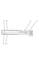
図1は本発明の一実施例を示す図であり、図中1a、1bはガラス基板、2a、2bは偏光板、3は駆動用半導体素子、4はフレキシブル配線基板(FPC)、5は入力信号用配線基板(PCB)、6は基板支持リブ、7はゴム、8aは前フレーム、8bは後フレーム、9aはカバーガラス、9bは後ガラス、10は伝熱用部材である。本図中において、液晶表示パネルはカバーガラス9a、後ガラス9b、およびゴム7によって略密閉空間中に支持され、特開平9−73072号公報にて示されているエアダンパ効果による衝撃吸収構造を形成している。
【0019】
本実施例においては、液晶表示素子のガラス基板1b上の周辺端部に延在された電極端子に接続され液晶表示素子に対して駆動波形を供給する駆動用半導体素子3がフェースダウン状態で異方性導電接着膜(図示せず)を用いて接続されCOG実装されており、駆動用半導体素子3に電源および制御信号を供給するためのフレキシブル配線基板4と入力信号用配線基板5が同様に異方性導電接着膜(図示せず)を用いて相互に接続され、液晶表示パネルを形成している。ここで、液晶表示パネルのガラス基板1a、1bはゴム7を介して、また入力信号用配線基板5は基板支持リブ6を介してカバーガラス9a、後ガラス9b、および前、後フレーム8a、8bに支持されている。さらに、駆動用半導体素子3が接続されたガラス基板1b上の周辺端部に延在された電極端子の概略裏面にあたるガラス基板面と後フレーム8b間に伝熱用部材10をほぼ密着するように設けている。
【0020】
液晶表示パネルに情報を表示するために駆動波形を供給することにより、駆動用半導体素子3はその消費電力に応じて発熱し、ガラス基板1b上に直接フェースダウン実装されているために、その熱がガラス基板1bに伝熱するが、さらに伝熱用部材10を介して後フレーム8bに伝熱する。また、液晶表示パネル自身も駆動によりその消費電力に応じて発熱するが、この熱もガラス基板1bから伝熱し、さらに伝熱用部材10を介して後フレーム8bに伝熱する。さてこの時フレーム8a、8bをできるかぎり熱伝導率が高い材質(金属等)で形成しておけば、その熱は支持フレーム全体に伝熱して放熱されるので、結果として液晶表示パネルや駆動用半導体素子の放熱を行うことができ、特に駆動用半導体素子の発熱が伝熱したガラス基板を直接放熱することができるので、駆動用半導体素子の発熱がガラス基板を介して液晶表示素子に伝熱し、液晶の光学応答特性の温度依存性により、画面内の温度ばらつきにより光学応答のばらつきを生じ、表示品質を低下させるという問題点を効果的に低減することができる。
【0021】
ここで、放熱をより効果的に行うためには、伝熱用部材10はガラス基板1a、1bよりも熱伝導率が高いことが当然望ましく、また液晶表示パネルの衝撃吸収支持構造が有効に働くためにガラス基板支持用のゴム7とほぼ同等の柔軟性を有するのが望ましい。具体的には、放熱用シリコンゴムや、あるいはフィルム製の袋の中に冷媒であるパーフロロカーボン液を充填したもの(商品名3M製リキッドヒートシンク)等を用いることができる。
【0022】
(実施例2)
図2は、実施例1に対して、駆動用半導体素子3と前フレーム8a間に伝熱用部材10を設けたもので、この放熱構造においては直接駆動用半導体素子3の発熱を前フレーム8aに伝熱することができるので、駆動用半導体素子3の放熱をより効果的に行うことができる。
【0023】
ただし、この放熱構造においては、液晶表示パネルの熱を直接放熱することはできないが、実施例1よりも駆動用半導体素子の発熱を直接放熱して駆動用半導体素子の発熱を低減することができるために、結果として駆動用半導体素子の発熱がガラス基板を介して液晶表示素子に伝熱することを低減することができる。
【0024】
しかしながら、駆動用半導体素子の発熱が電気素子に伝熱し熱影響を与えることを低減するためには実施例1の形態の方がより効果的であるので、どちらの放熱を優先するかにおいて実施例1あるいは実施例2の放熱構造を使い分けることができる。
【0025】
(実施例3)
図3は、実施例1および2の両方の位置に伝熱用部材10を設けたもので、液晶表示パネルおよび駆動用半導体素子3の両方から直接伝熱用部材10を介してフレーム8a、8bに伝熱し放熱することができるため、より効率的に放熱を行うことができ、実施例1および2で述べた効果を両方とも効果的に発揮させることができる。
【0026】
なお、上記実施例においては支持フレームとして前フレームと後フレームがある形状で説明したが、どちらか一方のみが存在するような形状でも、実施例1あるいは実施例2のいずれかを用いることにより同様の効果を発揮させることができる。
【0027】
また、上記実施例においては基板1bの周辺端部に延在された上面の電極端子に駆動用半導体素子3がフェースダウン状態で接続されているが、基板1aの周辺端部に延在された下面の電極端子に駆動用半導体素子3がフェースダウン状態で接続されてても、実施例を上下逆に用いれば同様の効果を発揮させることができる。
【0028】
また、上記実施例は全て液晶表示素子について述べたが、例えば非晶質シリコン(a−Si)を用いたエリアセンサとその駆動用半導体等の放熱構造においても同様に用いることができ、同様の構造を持った電気部品全般に応用できる。
【0029】
【発明の効果】
以上説明したように、本発明における電気部品の放熱構造を用いることにより、放熱部材の取付に余分な空間を取ること無く、また電気素子の支持構造に影響を与えずに伝熱用部材を取り付けて支持フレームを介して放熱することが可能で、半導体素子の発熱による電気素子への熱影響を軽減することにより、高品質な性能発揮を実現するとともに、電気素子の駆動用半導体素子の温度上昇を抑えることにより、半導体チップの寿命を長くし、信頼性を向上することができる。
【図面の簡単な説明】
【図1】本発明による第1の実施例を示す図である。
【図2】本発明による第2の実施例を示す図である。
【図3】本発明による第3の実施例を示す図である。
【図4】従来例を示す図である。
【符号の説明】
1a、1b ガラス基板
2a、2b 偏光板
3 駆動用半導体素子
4 フレキシブル配線基板(FPC)
5 入力信号用配線基板(PCB)
6 基板支持リブ
7 ゴム
8a 前フレーム
8b 後フレーム
9a カバーガラス
9b 後ガラス
10 伝熱用部材
11 放熱部材[0001]
BACKGROUND OF THE INVENTION
The present invention relates to a heat dissipation structure for an electrical component, and specifically, a liquid crystal display element and a driving semiconductor element thereof, more specifically, a liquid crystal display element using a ferroelectric liquid crystal and a driving semiconductor element thereof. This relates to a heat dissipation structure.
[0002]
[Prior art]
Conventionally, an electric element typified by a liquid crystal display element is formed on a substrate, and a drive circuit in which a semiconductor chip is mounted on a film carrier and separated individually by a TAB method as an external circuit for driving the liquid crystal display A device connected to an electrode terminal extending around the glass substrate of the device, or a semiconductor chip directly connected face-down to an electrode terminal extending around the glass substrate of the liquid crystal display device (COG mounting and There are electrical parts.
[0003]
However, in recent years, the liquid crystal display element has become larger and the driving load has increased, the power consumption of the driving semiconductor element has increased, the temperature rise of the semiconductor element has increased, and the life of the semiconductor chip being used has been shortened, Reliability is to be reduced. Furthermore, particularly in the case of a liquid crystal display element in which the driving semiconductor element is COG-mounted, the temperature of the display screen portion of the liquid crystal display element becomes non-uniform across the entire screen due to the heat effect from the semiconductor element, and the optical response characteristic has a temperature characteristic. For this reason, there is a case where the entire screen becomes non-uniform and the display quality is deteriorated.
[0004]
In particular, a liquid crystal display element using a ferroelectric liquid crystal has an advantage that a large screen can be obtained because of its high response speed and memory characteristics compared to liquid crystal display elements using other liquid crystals. Although research and development and commercialization have been promoted, a liquid crystal display element using ferroelectric liquid crystal has a gap between two transparent substrates sandwiching the liquid crystal as compared with a conventional liquid crystal display element using TN type liquid crystal. In general, the driving voltage is large and the dielectric constant of the liquid crystal material is high, so that the load capacity as viewed from the driving circuit is large and the current value output from the driving semiconductor element is large. For this reason, the power consumption is larger and the temperature rise of the semiconductor element is larger. Further, as the load capacity increases, it is necessary to reduce the wiring resistance of the liquid crystal display element in order to suppress the delay of the liquid crystal drive application voltage (in order to accelerate the rise of the applied voltage to the capacitive load). Therefore, the power consumption of the semiconductor element is further increased, and the temperature rise is further increased. When the temperature rise of the semiconductor element is large, the life of the semiconductor chip used is shortened and the reliability is lowered.
[0005]
Furthermore, the temperature of the screen part of the liquid crystal display element becomes non-uniform over the entire screen due to the heat effect from the driving semiconductor element mounted on the COG, and the optical response characteristics of the ferroelectric liquid crystal have temperature dependence. There is a problem in that the optical quality varies due to the temperature variation, and the display quality deteriorates.
[0006]
In order to deal with such problems, for example, as disclosed in Japanese Patent Laid-Open No. 5-313184, a method of directly dissipating heat by attaching a heat radiation member to a driving semiconductor element of a liquid crystal display element has been proposed.
[0007]
[Problems to be solved by the invention]
FIG. 4 shows a conventional example. An anisotropic conductive adhesive film (not shown) is used for the electrode terminal extending around the glass substrate 1b of the liquid crystal display element when the
[0008]
However, since the heat radiation member 11 is directly attached to the
[0009]
In addition, a liquid crystal display element using ferroelectric liquid crystal has a problem in that when a strong impact or external force is applied, the alignment of the liquid crystal is disturbed and normal display cannot be performed. Japanese Patent Laid-Open No. 9-73072 (this book) It is necessary to support the liquid crystal display panel with a shock absorbing structure as shown in FIG. In such a shock absorbing structure, since the liquid crystal display panel is movable to some extent, if the heat radiating member as shown in the conventional example is directly attached to the driving semiconductor element, the supporting structure is affected. Become.
[0010]
An object of the present invention is to provide an external circuit structure in which a driving semiconductor element is connected to an electric element in view of such problems of the prior art, without taking up extra space for mounting a heat radiating member. It is possible to attach a heat transfer member without affecting the support structure, and by reducing the heat effect on the electrical element due to the heat generated by the driving semiconductor element, high quality performance can be achieved and By suppressing the temperature rise of the element and the driving semiconductor element, the life of the semiconductor chip is extended and the reliability is improved.
[0011]
[Means for Solving the Problems]
The present invention according to
[0013]
According to a second aspect of the present invention, there is provided a glass substrate on which an electric element is formed , and an electrode terminal extending from the electric element to a peripheral edge on the glass substrate , and disposed on the glass substrate. In addition, a driving semiconductor element that supplies a driving waveform to the electric element, an input signal wiring board for supplying power and a control signal to the driving semiconductor element, the glass substrate, and an input signal wiring board An electrical component comprising a support frame for supporting an electrical component, wherein a heat transfer member having a higher thermal conductivity than the glass substrate is provided between the driving semiconductor element and the support frame. is there.
[0014]
According to a third aspect of the present invention, in the heat dissipation structure for an electric component according to the first aspect, a heat transfer member is also provided between the driving semiconductor element and the support frame.
[0015]
The present invention according to
[0016]
The present invention according to
[0017]
DETAILED DESCRIPTION OF THE INVENTION
(Example)
Hereinafter, embodiments of the present invention will be described with reference to the drawings. In the following embodiments, a liquid crystal display element will be described as an example.
[0018]
Example 1
FIG. 1 is a diagram showing an embodiment of the present invention, in which 1a and 1b are glass substrates, 2a and 2b are polarizing plates, 3 is a driving semiconductor element, 4 is a flexible printed circuit board (FPC), and 5 is an input. Signal wiring board (PCB), 6 is a board support rib, 7 is rubber, 8a is a front frame, 8b is a rear frame, 9a is a cover glass, 9b is a rear glass, and 10 is a heat transfer member. In this figure, the liquid crystal display panel is supported in a substantially sealed space by a cover glass 9a, a rear glass 9b, and
[0019]
In the present embodiment, the driving
[0020]
By supplying a driving waveform to display information on the liquid crystal display panel, the driving
[0021]
Here, in order to more effectively dissipate heat, it is naturally desirable that the
[0022]
(Example 2)
FIG. 2 shows a structure in which a
[0023]
However, in this heat dissipation structure, the heat of the liquid crystal display panel cannot be directly radiated, but the heat generation of the driving semiconductor element can be directly radiated and the heat generation of the driving semiconductor element can be reduced as compared with the first embodiment. As a result, it is possible to reduce the heat generated by the driving semiconductor element from being transferred to the liquid crystal display element through the glass substrate.
[0024]
However, since the
[0025]
(Example 3)
FIG. 3 shows a structure in which the
[0026]
In the above-described embodiment, the description has been given with the shape having the front frame and the rear frame as the support frame. However, even if only one of the shapes is present, it is the same by using either the
[0027]
In the above embodiment, the driving
[0028]
Although all the above embodiments have described liquid crystal display elements, for example, an area sensor using amorphous silicon (a-Si) and a heat dissipation structure such as a driving semiconductor thereof can be used similarly. Applicable to all electrical parts with structure.
[0029]
【The invention's effect】
As described above, by using the heat dissipation structure of the electrical component in the present invention, the heat transfer member can be attached without taking up an extra space for mounting the heat dissipation member and without affecting the support structure of the electric element. It is possible to dissipate heat through the support frame, and by reducing the thermal effect on the electrical element due to the heat generated by the semiconductor element, high quality performance is achieved and the temperature of the semiconductor element for driving the electrical element rises By suppressing this, the life of the semiconductor chip can be extended and the reliability can be improved.
[Brief description of the drawings]
FIG. 1 is a diagram showing a first embodiment according to the present invention.
FIG. 2 is a diagram showing a second embodiment according to the present invention.
FIG. 3 is a diagram showing a third embodiment according to the present invention.
FIG. 4 is a diagram showing a conventional example.
[Explanation of symbols]
DESCRIPTION OF SYMBOLS 1a, 1b Glass substrate 2a,
5 Input signal wiring board (PCB)
6
Claims (5)
前記駆動用半導体素子が配置されたガラス基板面の裏面にあたるガラス基板面と前記支持フレーム間に、前記ガラス基板より熱伝導度が高い伝熱用部材を設けたことを特徴とする電気部品の放熱構造。A glass substrate having electrical elements are formed, which is connected from the electrical device to the electrode terminals extending in the peripheral edge portion on the glass substrate, and arranged on the glass substrate, the drive to the electric element A driving semiconductor element for supplying a waveform, an input signal wiring board for supplying power and a control signal to the driving semiconductor element, a glass substrate on which the electric element is formed, and an input signal wiring board are supported. In electrical parts consisting of support frames,
Dissipating heat from an electrical component, wherein a heat transfer member having a higher thermal conductivity than the glass substrate is provided between the glass substrate surface corresponding to the back surface of the glass substrate surface on which the driving semiconductor element is disposed and the support frame. Construction.
前記駆動用半導体素子と前記支持フレーム間に、前記ガラス基板より熱伝導度が高い伝熱用部材を設けたことを特徴とする電気部品の放熱構造。 A glass substrate having electrical elements are formed, which is connected from the electrical device to the electrode terminals extending in the peripheral edge portion on said glass substrate, and arranged on the glass substrate, the drive to the electric element An electrical component comprising a driving semiconductor element for supplying a waveform, an input signal wiring board for supplying power and control signals to the driving semiconductor element, and a support frame for supporting the glass substrate and the input signal wiring board In
A heat dissipation structure for an electrical component, wherein a heat transfer member having higher thermal conductivity than the glass substrate is provided between the driving semiconductor element and the support frame.
Priority Applications (1)
| Application Number | Priority Date | Filing Date | Title |
|---|---|---|---|
| JP2002115359A JP3890251B2 (en) | 2002-04-17 | 2002-04-17 | Heat dissipation structure for electrical parts |
Applications Claiming Priority (1)
| Application Number | Priority Date | Filing Date | Title |
|---|---|---|---|
| JP2002115359A JP3890251B2 (en) | 2002-04-17 | 2002-04-17 | Heat dissipation structure for electrical parts |
Publications (3)
| Publication Number | Publication Date |
|---|---|
| JP2003309237A JP2003309237A (en) | 2003-10-31 |
| JP2003309237A5 JP2003309237A5 (en) | 2004-11-25 |
| JP3890251B2 true JP3890251B2 (en) | 2007-03-07 |
Family
ID=29396728
Family Applications (1)
| Application Number | Title | Priority Date | Filing Date |
|---|---|---|---|
| JP2002115359A Expired - Fee Related JP3890251B2 (en) | 2002-04-17 | 2002-04-17 | Heat dissipation structure for electrical parts |
Country Status (1)
| Country | Link |
|---|---|
| JP (1) | JP3890251B2 (en) |
Families Citing this family (7)
| Publication number | Priority date | Publication date | Assignee | Title |
|---|---|---|---|---|
| JP3756168B2 (en) * | 2004-03-19 | 2006-03-15 | 株式会社ソニー・コンピュータエンタテインメント | Circuit heat generation control method, apparatus and system |
| JP5124974B2 (en) * | 2006-04-21 | 2013-01-23 | セイコーエプソン株式会社 | Electro-optical device and electronic apparatus including the same |
| WO2010046948A1 (en) * | 2008-10-22 | 2010-04-29 | 日立プラズマディスプレイ株式会社 | Plasma display |
| JP5537860B2 (en) * | 2009-08-06 | 2014-07-02 | パナソニック株式会社 | Display device |
| JP5418328B2 (en) * | 2010-03-17 | 2014-02-19 | 日本精機株式会社 | Organic EL panel |
| CN104504998A (en) * | 2015-01-22 | 2015-04-08 | 京东方科技集团股份有限公司 | Display panel and display device |
| WO2019013115A1 (en) * | 2017-07-14 | 2019-01-17 | シャープ株式会社 | Display device |
-
2002
- 2002-04-17 JP JP2002115359A patent/JP3890251B2/en not_active Expired - Fee Related
Also Published As
| Publication number | Publication date |
|---|---|
| JP2003309237A (en) | 2003-10-31 |
Similar Documents
| Publication | Publication Date | Title |
|---|---|---|
| KR100542190B1 (en) | Plasma display apparatus having heat dissipating structure for driver ic | |
| JP4650822B2 (en) | Flat panel display | |
| KR20080008751A (en) | Display device | |
| KR20180058893A (en) | Display device | |
| JP2000137548A (en) | Thin electromagnetic interference shield having thermal diffusion plate | |
| JP2003108017A (en) | Flat panel type display device | |
| US20200196492A1 (en) | Display Device | |
| JP3890251B2 (en) | Heat dissipation structure for electrical parts | |
| KR20090013507A (en) | Plasma display apparatus | |
| US20080284765A1 (en) | Plasma display device and signal transmitting unit for plasma display device | |
| JPH0293425A (en) | Liquid crystal display device | |
| JPH10333173A (en) | Liquid crystal display device | |
| JPH05313184A (en) | External circuit structure for driving liquid crystal display element | |
| JP3139601B2 (en) | Liquid crystal display | |
| JP2000089226A (en) | Liquid crystal display device with el and portable electronic equipment mounting the device | |
| TWI386719B (en) | Flat display device | |
| JPH11109878A (en) | Liquid crystal display device | |
| KR100823196B1 (en) | Plasma display device | |
| KR100683759B1 (en) | Plasma display apparatus | |
| JP2002083907A (en) | Semiconductor device, board, liquid crystal display and plasma display using the same | |
| CN217639863U (en) | Display module | |
| CN217116726U (en) | Display module and electronic equipment | |
| CN218920673U (en) | Heat radiation structure and liquid crystal display of circuit board | |
| JP2006106064A (en) | Liquid crystal display | |
| JP2014053332A (en) | Display device |
Legal Events
| Date | Code | Title | Description |
|---|---|---|---|
| A977 | Report on retrieval |
Free format text: JAPANESE INTERMEDIATE CODE: A971007 Effective date: 20050407 |
|
| A131 | Notification of reasons for refusal |
Free format text: JAPANESE INTERMEDIATE CODE: A131 Effective date: 20060829 |
|
| A521 | Written amendment |
Free format text: JAPANESE INTERMEDIATE CODE: A523 Effective date: 20061030 |
|
| TRDD | Decision of grant or rejection written | ||
| A01 | Written decision to grant a patent or to grant a registration (utility model) |
Free format text: JAPANESE INTERMEDIATE CODE: A01 Effective date: 20061121 |
|
| A61 | First payment of annual fees (during grant procedure) |
Free format text: JAPANESE INTERMEDIATE CODE: A61 Effective date: 20061204 |
|
| R150 | Certificate of patent or registration of utility model |
Free format text: JAPANESE INTERMEDIATE CODE: R150 Ref document number: 3890251 Country of ref document: JP Free format text: JAPANESE INTERMEDIATE CODE: R150 |
|
| FPAY | Renewal fee payment (event date is renewal date of database) |
Free format text: PAYMENT UNTIL: 20091208 Year of fee payment: 3 |
|
| FPAY | Renewal fee payment (event date is renewal date of database) |
Free format text: PAYMENT UNTIL: 20101208 Year of fee payment: 4 |
|
| FPAY | Renewal fee payment (event date is renewal date of database) |
Free format text: PAYMENT UNTIL: 20111208 Year of fee payment: 5 |
|
| FPAY | Renewal fee payment (event date is renewal date of database) |
Free format text: PAYMENT UNTIL: 20121208 Year of fee payment: 6 |
|
| FPAY | Renewal fee payment (event date is renewal date of database) |
Free format text: PAYMENT UNTIL: 20131208 Year of fee payment: 7 |
|
| LAPS | Cancellation because of no payment of annual fees |