JP3877735B2 - Connected device - Google Patents
Connected device Download PDFInfo
- Publication number
- JP3877735B2 JP3877735B2 JP2004079745A JP2004079745A JP3877735B2 JP 3877735 B2 JP3877735 B2 JP 3877735B2 JP 2004079745 A JP2004079745 A JP 2004079745A JP 2004079745 A JP2004079745 A JP 2004079745A JP 3877735 B2 JP3877735 B2 JP 3877735B2
- Authority
- JP
- Japan
- Prior art keywords
- spiral
- contact
- outer peripheral
- support
- contacts
- Prior art date
- Legal status (The legal status is an assumption and is not a legal conclusion. Google has not performed a legal analysis and makes no representation as to the accuracy of the status listed.)
- Expired - Fee Related
Links
Images


Classifications
-
- H—ELECTRICITY
- H01—ELECTRIC ELEMENTS
- H01L—SEMICONDUCTOR DEVICES NOT COVERED BY CLASS H10
- H01L24/00—Arrangements for connecting or disconnecting semiconductor or solid-state bodies; Methods or apparatus related thereto
- H01L24/71—Means for bonding not being attached to, or not being formed on, the surface to be connected
- H01L24/72—Detachable connecting means consisting of mechanical auxiliary parts connecting the device, e.g. pressure contacts using springs or clips
-
- H—ELECTRICITY
- H01—ELECTRIC ELEMENTS
- H01R—ELECTRICALLY-CONDUCTIVE CONNECTIONS; STRUCTURAL ASSOCIATIONS OF A PLURALITY OF MUTUALLY-INSULATED ELECTRICAL CONNECTING ELEMENTS; COUPLING DEVICES; CURRENT COLLECTORS
- H01R33/00—Coupling devices specially adapted for supporting apparatus and having one part acting as a holder providing support and electrical connection via a counterpart which is structurally associated with the apparatus, e.g. lamp holders; Separate parts thereof
- H01R33/74—Devices having four or more poles, e.g. holders for compact fluorescent lamps
- H01R33/76—Holders with sockets, clips, or analogous contacts adapted for axially-sliding engagement with parallely-arranged pins, blades, or analogous contacts on counterpart, e.g. electronic tube socket
-
- G—PHYSICS
- G01—MEASURING; TESTING
- G01R—MEASURING ELECTRIC VARIABLES; MEASURING MAGNETIC VARIABLES
- G01R1/00—Details of instruments or arrangements of the types included in groups G01R5/00 - G01R13/00 and G01R31/00
- G01R1/02—General constructional details
- G01R1/06—Measuring leads; Measuring probes
- G01R1/067—Measuring probes
- G01R1/073—Multiple probes
- G01R1/07307—Multiple probes with individual probe elements, e.g. needles, cantilever beams or bump contacts, fixed in relation to each other, e.g. bed of nails fixture or probe card
- G01R1/07357—Multiple probes with individual probe elements, e.g. needles, cantilever beams or bump contacts, fixed in relation to each other, e.g. bed of nails fixture or probe card with flexible bodies, e.g. buckling beams
-
- H—ELECTRICITY
- H01—ELECTRIC ELEMENTS
- H01R—ELECTRICALLY-CONDUCTIVE CONNECTIONS; STRUCTURAL ASSOCIATIONS OF A PLURALITY OF MUTUALLY-INSULATED ELECTRICAL CONNECTING ELEMENTS; COUPLING DEVICES; CURRENT COLLECTORS
- H01R13/00—Details of coupling devices of the kinds covered by groups H01R12/70 or H01R24/00 - H01R33/00
- H01R13/02—Contact members
- H01R13/04—Pins or blades for co-operation with sockets
- H01R13/05—Resilient pins or blades
-
- H—ELECTRICITY
- H01—ELECTRIC ELEMENTS
- H01R—ELECTRICALLY-CONDUCTIVE CONNECTIONS; STRUCTURAL ASSOCIATIONS OF A PLURALITY OF MUTUALLY-INSULATED ELECTRICAL CONNECTING ELEMENTS; COUPLING DEVICES; CURRENT COLLECTORS
- H01R13/00—Details of coupling devices of the kinds covered by groups H01R12/70 or H01R24/00 - H01R33/00
- H01R13/02—Contact members
- H01R13/22—Contacts for co-operating by abutting
- H01R13/24—Contacts for co-operating by abutting resilient; resiliently-mounted
- H01R13/2407—Contacts for co-operating by abutting resilient; resiliently-mounted characterized by the resilient means
- H01R13/2421—Contacts for co-operating by abutting resilient; resiliently-mounted characterized by the resilient means using coil springs
-
- H—ELECTRICITY
- H01—ELECTRIC ELEMENTS
- H01L—SEMICONDUCTOR DEVICES NOT COVERED BY CLASS H10
- H01L2924/00—Indexing scheme for arrangements or methods for connecting or disconnecting semiconductor or solid-state bodies as covered by H01L24/00
- H01L2924/01—Chemical elements
- H01L2924/01004—Beryllium [Be]
-
- H—ELECTRICITY
- H01—ELECTRIC ELEMENTS
- H01L—SEMICONDUCTOR DEVICES NOT COVERED BY CLASS H10
- H01L2924/00—Indexing scheme for arrangements or methods for connecting or disconnecting semiconductor or solid-state bodies as covered by H01L24/00
- H01L2924/01—Chemical elements
- H01L2924/01005—Boron [B]
-
- H—ELECTRICITY
- H01—ELECTRIC ELEMENTS
- H01L—SEMICONDUCTOR DEVICES NOT COVERED BY CLASS H10
- H01L2924/00—Indexing scheme for arrangements or methods for connecting or disconnecting semiconductor or solid-state bodies as covered by H01L24/00
- H01L2924/01—Chemical elements
- H01L2924/01006—Carbon [C]
-
- H—ELECTRICITY
- H01—ELECTRIC ELEMENTS
- H01L—SEMICONDUCTOR DEVICES NOT COVERED BY CLASS H10
- H01L2924/00—Indexing scheme for arrangements or methods for connecting or disconnecting semiconductor or solid-state bodies as covered by H01L24/00
- H01L2924/01—Chemical elements
- H01L2924/01029—Copper [Cu]
-
- H—ELECTRICITY
- H01—ELECTRIC ELEMENTS
- H01L—SEMICONDUCTOR DEVICES NOT COVERED BY CLASS H10
- H01L2924/00—Indexing scheme for arrangements or methods for connecting or disconnecting semiconductor or solid-state bodies as covered by H01L24/00
- H01L2924/01—Chemical elements
- H01L2924/01033—Arsenic [As]
-
- H—ELECTRICITY
- H01—ELECTRIC ELEMENTS
- H01L—SEMICONDUCTOR DEVICES NOT COVERED BY CLASS H10
- H01L2924/00—Indexing scheme for arrangements or methods for connecting or disconnecting semiconductor or solid-state bodies as covered by H01L24/00
- H01L2924/01—Chemical elements
- H01L2924/01074—Tungsten [W]
-
- H—ELECTRICITY
- H01—ELECTRIC ELEMENTS
- H01L—SEMICONDUCTOR DEVICES NOT COVERED BY CLASS H10
- H01L2924/00—Indexing scheme for arrangements or methods for connecting or disconnecting semiconductor or solid-state bodies as covered by H01L24/00
- H01L2924/01—Chemical elements
- H01L2924/01078—Platinum [Pt]
-
- H—ELECTRICITY
- H01—ELECTRIC ELEMENTS
- H01L—SEMICONDUCTOR DEVICES NOT COVERED BY CLASS H10
- H01L2924/00—Indexing scheme for arrangements or methods for connecting or disconnecting semiconductor or solid-state bodies as covered by H01L24/00
- H01L2924/01—Chemical elements
- H01L2924/01082—Lead [Pb]
Landscapes
- Physics & Mathematics (AREA)
- General Physics & Mathematics (AREA)
- Engineering & Computer Science (AREA)
- Computer Hardware Design (AREA)
- Microelectronics & Electronic Packaging (AREA)
- Power Engineering (AREA)
- Measuring Leads Or Probes (AREA)
- Connecting Device With Holders (AREA)
Description
本発明は、BGAやLGA等の接続端子を備えた電子部品に対して電気的に接続されるスパイラル接触子に係わり、特にばね定数を高くすることができるとともに、単位面積当たりに実装密度を高めることを可能としたスパイラル接触子を備えた接続装置に関する。 The present invention relates to a spiral contactor that is electrically connected to an electronic component having a connection terminal such as a BGA or LGA. In particular, the spring constant can be increased and the mounting density per unit area can be increased. about the connection device e Bei the spiral contacts that made it possible.
図7は従来のスパイラル接触子を備えたコンタクトシートの一部を示す平面図、図8は従来のスパイラル接触子を拡大して示す平面図である。 FIG. 7 is a plan view showing a part of a contact sheet provided with a conventional spiral contact, and FIG. 8 is an enlarged plan view showing the conventional spiral contact.
図7に示すコンタクトシート1は薄い絶縁シートからなるガイドフレーム2を有しており、前記ガイドフレーム2上に複数のスパイラル接触子3が縦横方向に規則正しく配列されている。図8に示すように、個々のスパイラル接触子3は、略正方形状をした薄い銅板などで形成されており、外枠として機能する支持部3Aと、前記支持部3A内において渦巻き状に切り欠かれた変形部3Bとを有している。
A contact sheet 1 shown in FIG. 7 has a
前記コンタクトシート1は、縦横方向に規則正しく配列された複数のスルーホールを有する絶縁基板上に設置される。個々の前記スルーホールの縁部および内面には導電部が形成されており、個々のスパイラル接触子3の支持部3Aは個々のスルーホールの縁部にそれぞれ電気的に固定されている。また前記変形部3Bは前記スルーホール上に位置しており、スルーホールの貫通方向に弾性変形可能な状態にある。
The contact sheet 1 is installed on an insulating substrate having a plurality of through holes regularly arranged in the vertical and horizontal directions. Conductive portions are formed on the edges and inner surfaces of the individual through holes, and the
ICなど電子部品の底面に設けられた複数の球状接触子(BGA)やコーン状接触子(CGA)などの外部接触子が、複数のスパイラル接触子3に対向する状態で押し付けられると、前記外部接触子は前記スパイラル接触子3を押圧しながら前記スルーホール内に至る。このとき前記スパイラル接触子3の変形部3Bは弾性的に変形させられ、前記外部接触子の外面に巻き付きながら接触するため、個々の球状接触子と個々のスパイラル接触子との間が電気的に接続されるようになる。
When external contacts such as a plurality of spherical contacts (BGA) and cone-shaped contacts (CGA) provided on the bottom surface of an electronic component such as an IC are pressed against the plurality of
上記のようなスパイラル接触子に関する先行技術文献としては、例えば以下に示すようなものが存在している。
上記のようなスパイラル接触子では、変形部が大きく弾性変形させられた状態でスルーホール内に押し込まれるため、大きなばね定数を有することが必要とされるが、そのためには前記変形部3Bの幅寸法W(図8では平均的な幅寸法をWとして示している。)を可能な限り広く形成する必要がある。 In the spiral contact as described above, since the deformed portion is pushed into the through hole in a state of being largely elastically deformed, it is necessary to have a large spring constant. For that purpose, the width of the deformed portion 3B is required. It is necessary to form the dimension W (the average width dimension is shown as W in FIG. 8) as wide as possible.
しかし、上記従来のスパイラル接触子3は、変形部3Bの外周全域が四角形状の支持部3Aで囲まれた構成であるため、変形部3Bの幅寸法を広くすることには限界がある。
However, since the conventional
一方、スパイラル接触子3の外形寸法そのものを大きくし、すなわち支持部3Aの縦横方向の寸法を大きくすれば、内部の変形部3Bの幅寸法を広く形成することができるため、前記変形部3Bのばね定数を高めることが可能となる。しかし、この方法では、コンタクトシート1としたときの単位面積当たりの実装密度を高めることがでないという問題が生じる。
On the other hand, if the outer dimensions of the
さらに、図7に示すように、各スパイラル接触子3は前記支持部3Aどうしが、縦横方向で隣接する状態で配置されているため、隣り合う支持部3Aどうしの間で電気的な短絡(ショート)が発生しやすいという問題がある。
Further, as shown in FIG. 7, each
すなわち、各スパイラル接触子3は、例えば特許文献1などに記載されているように、ポリイミドなど絶縁性の基材シートの表面にニッケルや銅などのメッキ処理や前記銅メッキに対するエッチング処理など、複数の製造工程を経ることにより製造される。しかし、図7に示すように前記エッチング処理においては銅メッキ3Cが完全に除去しきれず残る場合があり、そのような場合には隣接する支持部3Aどうしが部分的に前記残存する銅メッキ3Cによって電気的に接続された状態で形成されてしまうことになる。
That is, each
そして、電子部品の外部接触子が、このようなスパイラル接触子の変形部3Bに接触させられ且つ電力が与えられると、前記支持部3Aどうしの間が前記銅メッキ3Cを介して電気的に短絡するため、前記電子部品の破壊や信号の混信などの不具合を発生させるという問題がある。
When the external contactor of the electronic component is brought into contact with the deformed part 3B of the spiral contactor and is supplied with electric power, the
本発明は上記従来の課題を解決するためのものであり、単位面積当たりの実装密度を高めることができるとともに、大きなばね定数を有するスパイラル接触子を備えた接続装置を提供することを目的としている。 The present invention has been made to solve the above-described conventional problems, and an object thereof is to provide a connecting device including a spiral contactor having a large spring constant while being able to increase the mounting density per unit area. .
さらにはスパイラル接触子の支持部どうしの短絡を防止することを可能とした接続装置を提供することを目的としている。 It is another object of the present invention to provide a connection device that can prevent a short circuit between support portions of a spiral contactor.
本発明は、基板に、複数のスパイラル接触子が設けられた接続装置において、
それぞれのスパイラル接触子は、基板上の接続部に固定される部分である支持部と、外周側の巻き始端から内周側の巻き終端に向かって螺旋状に延びて弾性変形可能な変形部とが、導電性材料で一体に形成され、
前記支持部は、前記巻き始端と連続し、前記巻き終端の中心を通る中心線を挟んで一方の側に設けられ、前記中心線を挟んで他方の側には、前記中心から最も離れた位置にある前記変形部の外周縁が露出しており、
前記支持部は前記中心線から離れた位置に外縁部を有し、前記外縁部には、前記中心に向けて窪む凹部が形成されており、
前記外周縁が、隣接する他のスパイラル接触子の前記凹部内に対向するように、複数の前記スパイラル接触子が並べられていることを特徴とするものである。
The present invention provides a connection device in which a plurality of spiral contacts are provided on a substrate.
Each spiral contact includes a support portion that is a portion fixed to a connection portion on the substrate, a deformable portion that extends in a spiral shape from the winding start end on the outer peripheral side toward the winding end end on the inner peripheral side, and is elastically deformable. Is integrally formed of a conductive material ,
The support portion is provided on one side of a center line that is continuous with the winding start end and passes through the center of the winding end, and is located farthest from the center on the other side of the center line. The outer peripheral edge of the deformed portion is exposed,
The support portion has an outer edge portion at a position away from the center line, and the outer edge portion is formed with a recess that is recessed toward the center.
A plurality of spiral contacts are arranged such that the outer peripheral edge faces the recessed portion of another adjacent spiral contact .
本発明では、変形部の占める面積を大きくすることができるため、幅寸法の広い変形部とすることができる。よって、変形部のばね定数を高めることができる。 In this invention, since the area which a deformation | transformation part occupies can be enlarged, it can be set as a deformation | transformation part with a wide width dimension. Therefore, the spring constant of the deformed portion can be increased.
本発明では、前記凹部は、円弧形状に沿って形成されており、前記円弧の曲率半径は、前記変形部の前記外周縁の曲率半径よりも大きいことが好ましい。 In this invention, it is preferable that the said recessed part is formed along circular arc shape, and the curvature radius of the said circular arc is larger than the curvature radius of the said outer periphery of the said deformation | transformation part.
上記手段では、隣り合うスパイラル接触子間で、互いの距離を近接させた状態で配置することができるため、単位面積当たりの実装密度を高めることができる。 In the above-described means, the adjacent spiral contacts can be arranged with their distances close to each other, so that the mounting density per unit area can be increased.
また、本発明は、前記外周縁が、隣接する他のスパイラル接触子の前記凹部内に対向するように、複数の前記スパイラル接触子が直線状に配列されて行が形成され、複数の前記行が、前記行が延びる方向と直交する方向である列方向に間隔を開けて平行に配置されているものである。In the present invention, a plurality of the spiral contacts are arranged in a straight line so that the outer peripheral edge faces the recessed portion of the other adjacent spiral contact, and a plurality of the rows are formed. However, they are arranged in parallel at intervals in the column direction, which is the direction perpendicular to the direction in which the rows extend.
また、隣り合う行では、前記支持部の向きが、互いに180度相違していることが好ましい。Moreover, it is preferable that the direction of the said support part is mutually different 180 degree | times in an adjacent line.
本発明のスパイラル接触子は、支持部が変形部の巻き始端側にのみ設けられており、それ以外の部分を開放した構造である。このため、従来は支持部であった部分、すなわち前記開放領域にも変形部を配置することが可能となるため、変形部の占める面積を多くすることが可能となる。よって、従来に比較して変形部の幅寸法を大きくすることができるため、変形部のばね定数を大きくすることが可能となる。 Spiral contactor of the present invention, the supporting portions are provided only et al is in the winding start side of the deformable section, a structure in which opening the other portions. For this reason, since it becomes possible to arrange | position a deformation | transformation part also to the part which was the support part conventionally, ie, the said open | release area | region, it becomes possible to increase the area which a deformation | transformation part occupies. Therefore, since the width dimension of a deformation | transformation part can be enlarged compared with the past, it becomes possible to enlarge the spring constant of a deformation | transformation part.
また支持部に形成された凹部内に、他のスパイラル接触子の変形部を配置することにより、単位面積当たりの実装密度を高めることができる。 Moreover, the mounting density per unit area can be raised by arrange | positioning the deformation | transformation part of another spiral contactor in the recessed part formed in the support part.
さらに本発明のコンタクトシートでは、行方向において支持部と変形部とを隣接させるとともに列方向では支持部間の距離を離すように配置したことより、製造時のエッチング処理において除去しきれなかった銅メッキによって前記支持部どうしが電気的に接続されるのを防止することが可能となる。 Furthermore, in the contact sheet of the present invention, the support portion and the deformable portion are arranged adjacent to each other in the row direction and the distance between the support portions is separated in the column direction. It is possible to prevent the support portions from being electrically connected to each other by plating.
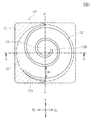
図1はスパイラル接触子の基本構成を参考例として示す平面図、図2は図1の2−2線における断面図である。 FIG. 1 is a plan view showing a basic configuration of a spiral contact as a reference example , and FIG. 2 is a cross-sectional view taken along line 2-2 of FIG.
図1に示すスパイラル接触子10は、支持部11と螺旋形状で形成された変形部12とを有している。前記変形部12は、外周側に巻き始端部12aが設けられ、渦巻きの中心である内周側に巻き終端部12bが設けられている。前記支持部11は前記変形部12の外周側に設けられており、前記変形部12の巻き始端部12aが前記支持部11から連続的に延出する構造である。なお、前記巻き終端部12bの先端は広い面積で形成されており、電子部品の外部接触子に対して中心的に接触する役割を果たす当接部12cとされている。
A
図1に示すものでは、前記支持部11は前記巻き始端部12aが設けられたX2側にのみ設けられており、前記巻き始端部12aが設けられていないX1側では変形部12の外側が開放された状態にある。また図1では前記支持部11が、前記当接部12cの中心を通りY方向に平行となる中心線O−Oまで形成されている。
In those shown in FIG. 1, the supporting
このため、前記中心線O−OよりもX1側の開放領域(変形部12の外側の領域)に前記変形部12を配置することができる。さらには支持部11を前記中心線O−Oよりも巻き始端部12a(X2)側の領域に形成することにより、前記変形部12がY方向に占める面積をも大きくすることが可能である。
For this reason, the said deformation |
よって、前記巻き始端部12aから巻き終端部12bまでの間の前記変形部12の幅寸法W1を全体的に広く形成することができる。よって、全体的な外形寸法、巻き数、板厚寸法および材質を同じくするスパイラル接触子どうしを比較したときに、従来よりも大きなばね定数を発揮することが可能なスパイラル接触子10とすることができる。すなわち、スパイラル接触子10の全体的な外形寸法を大型化することなく、従来よりも大きなばね定数を得ることができる。よって、ばね定数の大きな前記スパイラル接触子10とした場合でも、全体的な外形寸法を大きくする必要がなくなるため、スパイラル接触子を複数配置した場合においては単位面積当たりの実装密度の低下を防止できる。
Therefore, the width dimension W1 of the
また前記支持部11は巻き始端部12a側にのみに設けられ、それ以外の変形部12の外側は開放領域となっているため、隣り合うスパイラル接触子10を従来よりも近接させた状態で配置することが可能となる。よって、この点ではスパイラル接触子の実装密度を高めることが可能となる。
Further, since the
なお、前記幅寸法W1はスパイラル接触子10の平均的な幅寸法を示すものであり、上記従来のスパイラル接触子3の平均的な幅寸法W(図8参照)に対応するものである。
The width dimension W1 indicates the average width dimension of the
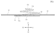
スパイラル接触子10は、図2に実線で示すような平面形状で形成されている。あるいは図2に点線で示すように前記当接部12cが図示Z1方向に突出する立体凸型形状に塑性変形させられた状態で形成されている。そして、このような前記スパイラル接触子10の支持部11は、ポリイミドなどの絶縁シートなどからなるガイドフレーム21に固定されている。すなわち、前記ガイドフレーム21には開口部22が形成されており、前記支持部11は前記開口部22の縁周部の裏面(Z2側の面)に対して接着剤などを介して固着されている。なお、図1にて点線のハッチングで示す部分が接着剤ののりしろ部分である。
The
図2に示すように、スパイラル接触子10が平面形状である場合には、前記変形部12は前記開口部22に平行に対向するように固定されている。また前記スパイラル接触子10が立体凸型形状である場合には、前記変形部12の巻き始端部12aよりも先端側が、前記開口部22を通じて前記ガイドフレーム21の表面(Z1)方向に突出するように固定されている。
As shown in FIG. 2, when the
図3は図1のスパイラル接触子を用いて形成したコンタクトシートを示す平面図である。なお、以下においては、横(X)方向を行、縦(Y)方向を列として規定し説明する。 FIG. 3 is a plan view showing a contact sheet formed using the spiral contact of FIG. In the following description, the horizontal (X) direction is defined as a row and the vertical (Y) direction is defined as a column.
図3に示すように、ガイドフレーム21には複数の開口部22が行方向および列方向に所定のピッチで規則正しく並ぶように形成されている。そして、一つの開口部22に一つの前記スパイラル接触子10が対応して固定されることにより、コンタクトシート20が形成されている。
As shown in FIG. 3, a plurality of
図4は絶縁基板上に配置されたコンタクトシートを部分的に示す断面図である。前記コンタクトシート20は絶縁基板30上に配置される。前記絶縁基板30には、複数のスルーホール31が縦横方向に規則正しく配列されており、隣り合うスルーホール間の縦横方向のピッチ寸法は、前記ガイドフレーム21に設けられたスパイラル接触子10の縦横方向のピッチ寸法と同じである。よって、一つのスルーホール31には一つのスパイラル接触子10が対向している。
FIG. 4 is a cross-sectional view partially showing a contact sheet disposed on an insulating substrate. The
図4に示すように、スルーホール31の内面には銅メッキなどにより形成された導電部32が形成されている。また前記スルーホール31の上下の開口縁部には前記導電部32に導通する接続部33,34が周設されている。そして、一方の接続部33とスパイラル接触子10の前記支持部11とが導電性接着剤などにより接続固定されている。
As shown in FIG. 4, a
また他方の接続部34には接続端子35が固定されており、絶縁基板30の下方に設けられて配線基板40上に形成された複数のパターン線41の個々のパターン線41に対し、導電性接着剤または半田付けなどの手段により接続されている。よって、前記スパイラル接触子10とパターン線41とは一方の接続部33、導電部32、他方の接続部34および接続端子35を介して電気的に導通されている。すなわち、前記コンタクトシートおよびスルーホールを有する絶縁基板とは,前記外部接触子と配線基板40のパターン線41とを電気的に接続するための接続装置として機能している。なお、前記パターン線41は外部に設けられる図示しない外部回路に接続されており、電子部品50と外部回路とが接続されるようになっている。
In addition, a
また前記接続端子35の代わりに、絶縁基板30の下側にもコンタクトシート20を配置し、前記コンタクトシート20に設けられているスパイラル接触子10を用いて前記他方の接続部34とパターン線41とが接続される構成としたものであってもよい。
Further, instead of the
図4に示すように、電子部品50に設けられた球状接触子(BGA)などの外部接触子51が、前記スパイラル接触子10に図示Z2方向に押し付けられると、前記スパイラル接触子10の変形部12が凹状に弾性変形しつつ前記外部接触子51の外面を抱き込むように接触させられる。よって、前記電子部品50の外部接触子51とパターン線41とを電気的に接続することが可能となる。
As shown in FIG. 4, when an
図3に示すように、前記コンタクトシート20は、第1行目のすべてのスパイラル接触子10が支持部11をX2側に向けた状態で並べられている。また前記第1行目に隣接する第2行目は、すべてのスパイラル接触子10が支持部11をX1側に向けた状態で並べられている。そして、第3行目は、すべてのスパイラル接触子10が支持部11をX2側に向けた状態で並べられている。以下同様に、スパイラル接触子10は、その向きが隣接する行ごとに交互に異なるように前記ガイドフレーム21に設けられている。すなわち、コンタクトシート20では、スパイラル接触子10の向きが上下左右で異なるように、いわゆる千鳥掛け状に配置されている。
As shown in FIG. 3, in the
このため、行方向に隣り合うスパイラル接触子10どうしの間では、支持部11どうしが互いに近接する状態でガイドフレーム21上に固定されることがない。また列方向に隣り合うスパイラル接触子10どうしの間においても、支持部11どうしが互いに近接して並ぶ状態を避けることが可能となる。すなわち、隣り合うスパイラル接触子10の支持部11どうしが行方向および列方向において近接することがなく、支持部11間の距離を上記図7の従来の場合以上に離すことが可能である。
For this reason, between the
よって、たとえ製造時のエッチング処理の際に、銅メッキが除去し切れずガイドフレーム上に部分的に残存することがあるとしても、支持部11間の距離が長く、しかも支持部11どうしが隣り合って並ぶことがないため、前記支持部11どうしが電気的に接続されるのを防止することが可能となる。
Therefore, even if the copper plating may not be completely removed during the etching process during manufacturing, and may remain partially on the guide frame, the distance between the
また、仮に近接する支持部11と変形部12との間が残存する銅メッキで接続されたとしても、上記のように電子部品50の外部接触子51が変形部12を押圧したときに前記変形部12が変形させられるため、銅メッキ部分が切断されて前記支持部11と変形部12との間の接続を分離することが可能である。よって、その後に電源が投入されても電子部品50の破壊や信号の混信等の不具合を防止することができる。
Even if the
図5は、本発明の実施の形態としてのスパイラル接触子を示す平面図、図6は図5のスパイラル接触子並べた状態を示す平面図である。 FIG. 5 is a plan view showing a spiral contact as an embodiment of the present invention, and FIG. 6 is a plan view showing a state in which the spiral contact of FIG. 5 is arranged.
図5に実施の形態として示すスパイラル接触子60は、前記第1の実施の形態で示すスパイラル接触子10とほぼ同じ構成である。すなわち、スパイラル接触子60は、変形部62と、前記変形部62の巻き始端部62aに連続する支持部61とを有するとともに、前記支持部61は前記巻き始端部62a側(図示左側)にのみ設けられ、右側の変形部62は開放状態となっている。ただし、変形部62の図示左端(変形部12が設けられている側とは逆側の端部)には、前記変形部12方向(図示右方向)に凹部61aが形成されている点で異なっている。
A
前記凹部61aは、変形部12の最外周部の曲率半径r1よりも大きな曲率半径r2からなる円弧に沿って形成されている。このため、図6に示すように、複数のスパイラル接触子60を並べたときに、隣り合うスパイラル接触子60の一方の凹部61aに他方のスパイラル接触子60の変形部62を部分的に配置することができる。このため、スパイラル接触子60では、スパイラル接触子60の行方向の距離を密接させた状態で配置することが可能となり、単位面積当たりの実装密度を高めることができるため、ガイドフレーム上に配置可能なスパイラル接触子60の数を増やすことが可能となる。
The
また図3と同様に千鳥掛け状に配置することにより、製造時において隣り合うスパイラル接触子60の支持部61どうしが接続されるのを防止しやすくできるとともに、支持部61と変形部62とが接続状態にある場合にはその分離をすることが可能となる。
Further, by arranging them in a staggered manner as in FIG. 3, it is easy to prevent the
10 スパイラル接触子
11 支持部
12 変形部
12a 巻き始端部
12b 巻き終端部
12c 当接部
20 コンタクトシート
21 ガイドフレーム
22 開口部
30 絶縁基板
31 スルーホール
32 導電部
33,34 接続部
40 配線基板
41 パターン線
50 電子部品
51 外部接触子
60 スパイラル接触子
61 支持部
61a 凹部
62 変形部
DESCRIPTION OF
Claims (4)
それぞれのスパイラル接触子は、基板上の接続部に固定される部分である支持部と、外周側の巻き始端から内周側の巻き終端に向かって螺旋状に延びて弾性変形可能な変形部とが、導電性材料で一体に形成され、
前記支持部は、前記巻き始端と連続し、前記巻き終端の中心を通る中心線を挟んで一方の側に設けられ、前記中心線を挟んで他方の側には、前記中心から最も離れた位置にある前記変形部の外周縁が露出しており、
前記支持部は前記中心線から離れた位置に外縁部を有し、前記外縁部には、前記中心に向けて窪む凹部が形成されており、
前記外周縁が、隣接する他のスパイラル接触子の前記凹部内に対向するように、複数の前記スパイラル接触子が並べられていることを特徴とする接続装置。 In the connection device provided with a plurality of spiral contacts on the substrate,
Each spiral contact includes a support portion that is a portion fixed to a connection portion on the substrate, a deformable portion that extends in a spiral shape from the winding start end on the outer peripheral side toward the winding end end on the inner peripheral side, and is elastically deformable. Is integrally formed of a conductive material ,
The support portion is provided on one side of a center line that is continuous with the winding start end and passes through the center of the winding end, and is located farthest from the center on the other side of the center line. The outer peripheral edge of the deformed portion is exposed,
The support portion has an outer edge portion at a position away from the center line, and the outer edge portion is formed with a recess that is recessed toward the center.
A connection device in which a plurality of spiral contacts are arranged so that the outer peripheral edge faces the recessed portion of another adjacent spiral contact.
Priority Applications (5)
| Application Number | Priority Date | Filing Date | Title |
|---|---|---|---|
| JP2004079745A JP3877735B2 (en) | 2004-03-19 | 2004-03-19 | Connected device |
| KR1020050015361A KR100803958B1 (en) | 2004-03-19 | 2005-02-24 | Spiral contactor, contact seat with the spiral contactor and connection device with the contact seat |
| US11/077,277 US7080993B2 (en) | 2004-03-19 | 2005-03-09 | Spiral contactor, contact sheet having spiral contactor, and connecting device having contact sheet |
| CNB200510054764XA CN100369335C (en) | 2004-03-19 | 2005-03-11 | Spiral contactor, contact sheet and connecting device |
| TW094108224A TWI286868B (en) | 2004-03-19 | 2005-03-17 | Spiral contactor, contact sheet having spiral contactor, and connecting device having contact sheet |
Applications Claiming Priority (1)
| Application Number | Priority Date | Filing Date | Title |
|---|---|---|---|
| JP2004079745A JP3877735B2 (en) | 2004-03-19 | 2004-03-19 | Connected device |
Related Child Applications (1)
| Application Number | Title | Priority Date | Filing Date |
|---|---|---|---|
| JP2006202840A Division JP3904592B2 (en) | 2006-07-26 | 2006-07-26 | Connecting device with spiral contact |
Publications (3)
| Publication Number | Publication Date |
|---|---|
| JP2005268079A JP2005268079A (en) | 2005-09-29 |
| JP2005268079A5 JP2005268079A5 (en) | 2006-07-20 |
| JP3877735B2 true JP3877735B2 (en) | 2007-02-07 |
Family
ID=34986940
Family Applications (1)
| Application Number | Title | Priority Date | Filing Date |
|---|---|---|---|
| JP2004079745A Expired - Fee Related JP3877735B2 (en) | 2004-03-19 | 2004-03-19 | Connected device |
Country Status (5)
| Country | Link |
|---|---|
| US (1) | US7080993B2 (en) |
| JP (1) | JP3877735B2 (en) |
| KR (1) | KR100803958B1 (en) |
| CN (1) | CN100369335C (en) |
| TW (1) | TWI286868B (en) |
Families Citing this family (8)
| Publication number | Priority date | Publication date | Assignee | Title |
|---|---|---|---|---|
| JP4540707B2 (en) * | 2005-03-18 | 2010-09-08 | 富士通株式会社 | Electronic components and circuit boards |
| JP4528657B2 (en) * | 2005-03-23 | 2010-08-18 | アルプス電気株式会社 | Contact member and manufacturing method thereof |
| JP4644762B2 (en) * | 2005-11-01 | 2011-03-02 | 株式会社アドバンストシステムズジャパン | Spiral contact and method for manufacturing the same |
| US7322831B1 (en) * | 2006-07-18 | 2008-01-29 | Cheng Uei Precision Industry Co., Ltd. | Matrix board-to-board connector |
| TW200903912A (en) | 2007-03-13 | 2009-01-16 | Alps Electric Co Ltd | Contact sheet and connection device having same |
| JP2010211940A (en) * | 2009-03-06 | 2010-09-24 | Alps Electric Co Ltd | Elastic contact element |
| CN106785540A (en) * | 2017-01-19 | 2017-05-31 | 启东乾朔电子有限公司 | Electronic card coupler and its conducting terminal |
| US10270193B1 (en) * | 2017-12-18 | 2019-04-23 | Continental Automotive Systems, Inc. | Concentric springs for sensor connection |
Family Cites Families (8)
| Publication number | Priority date | Publication date | Assignee | Title |
|---|---|---|---|---|
| JPS59230741A (en) * | 1983-06-15 | 1984-12-25 | 株式会社日立製作所 | Shape memory composite material |
| JP2533511B2 (en) * | 1987-01-19 | 1996-09-11 | 株式会社日立製作所 | Electronic component connection structure and manufacturing method thereof |
| US4961709A (en) * | 1989-02-13 | 1990-10-09 | Burndy Corporation | Vertical action contact spring |
| US5810609A (en) | 1995-08-28 | 1998-09-22 | Tessera, Inc. | Socket for engaging bump leads on a microelectronic device and methods therefor |
| US6354845B1 (en) * | 2000-06-01 | 2002-03-12 | Lucent Technologies Inc. | Apparatus and method for connecting a plurality of electrical circuits borne upon a plurality of substrates |
| JP3440243B2 (en) * | 2000-09-26 | 2003-08-25 | 株式会社アドバンストシステムズジャパン | Spiral contactor |
| JP4210049B2 (en) | 2001-09-04 | 2009-01-14 | 株式会社アドバンストシステムズジャパン | Spiral contact |
| JP3814231B2 (en) * | 2002-06-10 | 2006-08-23 | 株式会社アドバンストシステムズジャパン | Spiral contactor and manufacturing method thereof, semiconductor inspection apparatus using the same, and electronic component |
-
2004
- 2004-03-19 JP JP2004079745A patent/JP3877735B2/en not_active Expired - Fee Related
-
2005
- 2005-02-24 KR KR1020050015361A patent/KR100803958B1/en not_active IP Right Cessation
- 2005-03-09 US US11/077,277 patent/US7080993B2/en not_active Expired - Fee Related
- 2005-03-11 CN CNB200510054764XA patent/CN100369335C/en not_active Expired - Fee Related
- 2005-03-17 TW TW094108224A patent/TWI286868B/en not_active IP Right Cessation
Also Published As
| Publication number | Publication date |
|---|---|
| US20050208796A1 (en) | 2005-09-22 |
| JP2005268079A (en) | 2005-09-29 |
| TWI286868B (en) | 2007-09-11 |
| TW200534546A (en) | 2005-10-16 |
| KR20060042141A (en) | 2006-05-12 |
| US7080993B2 (en) | 2006-07-25 |
| CN100369335C (en) | 2008-02-13 |
| KR100803958B1 (en) | 2008-02-15 |
| CN1671009A (en) | 2005-09-21 |
Similar Documents
| Publication | Publication Date | Title |
|---|---|---|
| CN111562681B (en) | Shape memory alloy wire attachment structure for suspension assembly | |
| US7121837B2 (en) | Connector | |
| US7383632B2 (en) | Method for fabricating a connector | |
| JP4258432B2 (en) | Substrate bonding member and three-dimensional connection structure using the same | |
| JP5845029B2 (en) | Housingless connector | |
| US7080993B2 (en) | Spiral contactor, contact sheet having spiral contactor, and connecting device having contact sheet | |
| US9077127B2 (en) | Connector assembly | |
| KR101462523B1 (en) | Connector | |
| JP3134262U (en) | Surface mount connector | |
| EP2425689B1 (en) | Connecting unit | |
| JP3829327B2 (en) | Card edge connector and card member | |
| US9831583B2 (en) | Connector | |
| JP2007516591A (en) | Printed circuit board assembly | |
| US8110751B2 (en) | Semiconductor memory module and electronic component socket for coupling with the same | |
| JP3904592B2 (en) | Connecting device with spiral contact | |
| US20140335705A1 (en) | Electrical connector | |
| TWI384693B (en) | Terminal carriers and method of assembling the terminals | |
| JP3701738B2 (en) | Electrical connector | |
| JP2012243487A (en) | Socket for electronic component | |
| JP2024124325A (en) | Connectors and Connector Units | |
| JP2000022353A (en) | Structure for connecting wiring material of wlectric connection box and printed board part of electronic unit | |
| JP5717279B2 (en) | Wiring board and manufacturing method thereof | |
| JP3391513B2 (en) | Electric motor manufacturing method | |
| JPH11204223A (en) | Ic socket | |
| JP5590722B2 (en) | Wiring board and manufacturing method thereof |
Legal Events
| Date | Code | Title | Description |
|---|---|---|---|
| A521 | Written amendment |
Free format text: JAPANESE INTERMEDIATE CODE: A523 Effective date: 20060607 |
|
| A621 | Written request for application examination |
Free format text: JAPANESE INTERMEDIATE CODE: A621 Effective date: 20060607 |
|
| A871 | Explanation of circumstances concerning accelerated examination |
Free format text: JAPANESE INTERMEDIATE CODE: A871 Effective date: 20060607 |
|
| A131 | Notification of reasons for refusal |
Free format text: JAPANESE INTERMEDIATE CODE: A131 Effective date: 20060704 |
|
| A521 | Written amendment |
Free format text: JAPANESE INTERMEDIATE CODE: A523 Effective date: 20060726 |
|
| TRDD | Decision of grant or rejection written | ||
| A01 | Written decision to grant a patent or to grant a registration (utility model) |
Free format text: JAPANESE INTERMEDIATE CODE: A01 Effective date: 20061003 |
|
| A61 | First payment of annual fees (during grant procedure) |
Free format text: JAPANESE INTERMEDIATE CODE: A61 Effective date: 20061031 |
|
| R150 | Certificate of patent or registration of utility model |
Free format text: JAPANESE INTERMEDIATE CODE: R150 |
|
| A975 | Report on accelerated examination |
Free format text: JAPANESE INTERMEDIATE CODE: A971005 Effective date: 20060626 |
|
| FPAY | Renewal fee payment (event date is renewal date of database) |
Free format text: PAYMENT UNTIL: 20101110 Year of fee payment: 4 |
|
| FPAY | Renewal fee payment (event date is renewal date of database) |
Free format text: PAYMENT UNTIL: 20101110 Year of fee payment: 4 |
|
| FPAY | Renewal fee payment (event date is renewal date of database) |
Free format text: PAYMENT UNTIL: 20111110 Year of fee payment: 5 |
|
| FPAY | Renewal fee payment (event date is renewal date of database) |
Free format text: PAYMENT UNTIL: 20111110 Year of fee payment: 5 |
|
| FPAY | Renewal fee payment (event date is renewal date of database) |
Free format text: PAYMENT UNTIL: 20121110 Year of fee payment: 6 |
|
| LAPS | Cancellation because of no payment of annual fees |