JP3874340B2 - Polishing equipment - Google Patents
Polishing equipment Download PDFInfo
- Publication number
- JP3874340B2 JP3874340B2 JP2001309902A JP2001309902A JP3874340B2 JP 3874340 B2 JP3874340 B2 JP 3874340B2 JP 2001309902 A JP2001309902 A JP 2001309902A JP 2001309902 A JP2001309902 A JP 2001309902A JP 3874340 B2 JP3874340 B2 JP 3874340B2
- Authority
- JP
- Japan
- Prior art keywords
- electrode
- polished
- polishing
- abrasive grains
- polishing apparatus
- Prior art date
- Legal status (The legal status is an assumption and is not a legal conclusion. Google has not performed a legal analysis and makes no representation as to the accuracy of the status listed.)
- Expired - Fee Related
Links
Images


Classifications
-
- B—PERFORMING OPERATIONS; TRANSPORTING
- B23—MACHINE TOOLS; METAL-WORKING NOT OTHERWISE PROVIDED FOR
- B23H—WORKING OF METAL BY THE ACTION OF A HIGH CONCENTRATION OF ELECTRIC CURRENT ON A WORKPIECE USING AN ELECTRODE WHICH TAKES THE PLACE OF A TOOL; SUCH WORKING COMBINED WITH OTHER FORMS OF WORKING OF METAL
- B23H5/00—Combined machining
- B23H5/06—Electrochemical machining combined with mechanical working, e.g. grinding or honing
- B23H5/08—Electrolytic grinding
-
- B—PERFORMING OPERATIONS; TRANSPORTING
- B24—GRINDING; POLISHING
- B24B—MACHINES, DEVICES, OR PROCESSES FOR GRINDING OR POLISHING; DRESSING OR CONDITIONING OF ABRADING SURFACES; FEEDING OF GRINDING, POLISHING, OR LAPPING AGENTS
- B24B37/00—Lapping machines or devices; Accessories
- B24B37/04—Lapping machines or devices; Accessories designed for working plane surfaces
Description
【0001】
【発明の属する技術分野】
本発明は、電極間に電圧を印加し、誘電性を有する砥粒をクーロン力によって加工圧の加わる位置に配置して被研磨材を研磨する研磨装置に関するものである。
【0002】
【従来の技術】
一般に研磨装置は、種々の構造のものが提案されているが、研磨定盤の上に散布した砥粒を保持するポリシングパッドを固定し、被研磨材と研磨定盤とは相対移動させることにより前記砥粒が転動し前記被研磨材の表面の粗さを改善する装置が存在した。
また、近年電界や磁界に応答する各種機能性流体の研究が進み、一部で実用化されている。
【0003】
例えば、研磨や表面仕上げなどの加工においては、磁界に応答する磁性流体を用いる例が知られている。この磁性流体は、オングストロームオーダーの磁性粒子を分散させた流体である。この流体を単独で研磨に用いても研磨作用が殆ど期待できないため、砥粒を加えて研磨に使用している。その作用は、磁界により被研磨材表面に沿って誘起される磁性流体によって砥粒に加工圧力が加えられる。しかし、このような磁性流体による研磨加工は、被加工面が球面などの特殊形状を有する場合には好適であるものの、磁界によって誘起される加工圧力が小さいため、研磨効率が低いという問題や加工屑が磁性流体に混入してスクラッチ痕を形成する事、被研磨材が磁性材の場合には,砥粒の運動は拘束されて研磨効果が得られないなどの問題点があり、用途の拡大が進んでいない。
【0004】
また、磁界応答性流体(MR流体)は、マイクロメーターオーダーの鉄粉等の強磁性粒子を分散させた流体である。この流体に砥粒を混合し,磁界を印加すると、強磁性粒子は、速やかに誘起、粒子間で吸引し合い凝集するため、太い磁性針状態を形成するために、被研磨材に対して強い加工力を与えることができるため高い加工効率を得られる。しかし、その磁性針状体の形状・配置ならびに見かけ上の粘度などの制御が困難とされるため、このような状態において加工圧が加わると、被加工面にスクラッチ痕が形成される危険性が高い。即ち、このようなMR流体では、粗い一次研磨(研削)には用いられ得るが、精微な研磨、すなわち、仕上げ加工には容易には利用できないとされている。また、MR流体における分散粒子には一般的に粒子径の大きな鉄粉等が用いられることも精微な研磨、仕上げなどの加工を阻害する要因である。
【0005】
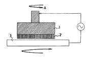
図12は、従来の研磨装置の一例を示す説明図である。ここで、研磨装置には、回転電極1とこの回転電極の直下に配置されたポリシングパッド2を備えており、さらに研磨材にはシリコーンオイルまたは電気絶縁性を有する潤滑剤に分散した砥粒を用いる。導電性試料3と回転電極1との間に交流電圧を印加すると砥粒は電極に引き寄せられたり反発したりする。また、回転電極1は、図外の駆動機構により矢印A方向に回転可能に支持されている。
図13は、従来の電極の作用を模式的に示す説明図である。ここで、印加電界によって分散砥粒4は、導電性試料3に対して垂直に連続配列するクラスターを形成する。
ここで、電極間に発生したクラスターは隣同士が互いに反発し、ある間隔を保つため砥粒の配置が不均一になり易く、被研磨材の表面粗さにバラツキが生じ易かった。
【0006】
【発明が解決しようとする課題】
しかし、以上のように構成された従来の研磨装置においては、回転電極1から導電性試料3に叩きつける砥粒の動きや前述した不均一な砥粒配置があり、大型の製品に対する高品位な研磨面を得ることが困難であった。また、被研磨材に対して回転電極との間に電圧を印加する必要が有るため、絶縁性材料に適用することが困難であった。
すなわち、絶縁性被研磨材の厚みがそのまま空隙と同様に作用し、高い電界強度を供給しなければ砥粒の配置を制御できず高い研磨効果が得られないと云う問題と作業上の危険性や被研磨材に対する放電現象によってダメージを与える危険性も有していた。
また、一般的な研磨装置では、研磨部の回転による遠心力によって砥粒が加工領域から排他されて加工部外周に集まり易く、研磨効率を下げていた。この現象に対して従来の研磨装置では、印加電界を供給すると高い誘電率を有する砥粒は、再度クーロン力によって研磨領域に戻ることを利用し、被研磨材に与える砥粒量の均一化を図っていたが前記のように隣同士の砥粒の配置にある間隔を有するため高度に均一な砥粒配置は実現でき無かった。
本発明は上記実情に鑑み提案されたもので、絶縁性材料の研磨が可能であると共に砥粒の均一配置制御が容易な研磨装置を提供することを目的とする。
【0007】
【課題を解決するための手段】
上記目的を達成するために、請求項1に記載の発明は、電極を駆動装置によって駆動すると共に、前記電極と被研磨材との間に砥粒を配置し、前記電極に交流電圧を印加することで誘電性を有する砥粒をクーロン力で加工圧の加わる位置に配置し、被研磨材を研磨する研磨装置であって、前記電極は複数の電極素子から構成したことを特徴とする。
以上の構成により、被研磨材質や厚さの影響を受けることなく、均一な研磨を行うことができる。
【0008】
また、請求項2に記載の発明において、前記電極は、径の異なる複数の電極素子を同心円状に配置すると共に、各電極素子間は絶縁性材料で離隔した電極であることを特徴としている。
【0009】
また、請求項3に記載の発明は、上記した請求項1または2に記載の発明の構成に加えて、前記電極の複数の電極素子には、異なる電圧が印加されることを特徴とする。または、絶縁材の厚みを調整し各電極素子の砥粒吸引力を調整することで、回転電極の遠心力による砥粒の飛散などの影響を抑制することもできる。
【0010】
また、請求項4に記載の発明は、上記した請求項1から3の何れか1に記載の発明の構成に加えて、前記電極の複数の電極素子には、中心部から外周部に向かって順次高い電圧が印加されることを特徴とする。
以上の構成により、遠心力の影響が作用しやすい外周部において高い電圧を印加し、影響の少ない内周部に低い電圧を印加する事が可能となり、研磨量の均一化を実現することができる。
【0012】
また、請求項5に記載の発明は、被研磨材へ砥粒を分散した流体を供給する機構であって、絶縁性管の周囲に電極を配設し、電界強度1.5〜3kV/mm、0.1〜10Hzの低周波交流電界を印加すると、前記絶縁性管から滴下する流体のみかけ上の粘度変化を生じ、流量を調整する。
【0013】
【発明の実施の形態】
以下、図面に基づいて本発明を詳細に説明する。図1は、本発明に係る研磨装置の回転電極の第1の実施例を示す説明図、図2は本発明の回転電極を示す要部縦断面図である。ここで、研磨装置10は、回転電極11を図外の駆動装置によって回転駆動すると共に、回転電極11と被研磨材12との間に電気絶縁性を有する潤滑油に砥粒を分散させた流体を滴下し、回転電極11に交流電圧を印加することにより、クーロン力が作用し、砥粒13がポリシングパッド17と被研磨材12との間で数珠状に配置制御される。印加する電界は、電界強度±1〜10kV/mm、周波数0.1〜1000Hzであることが望ましい。更に、印加する周波数と波形は、加工量の大きい研磨においては立ち上がりの良い方形波や加工量の少ない研磨にあっては、立ち上がりがゆるやかでノイズ分が含まれない正弦波とすることが望ましい。
【0014】
回転電極11は、支持軸14と支持円盤15と電極部16とポリシングパッド17等から構成されている。支持軸14は、図示しない駆動機構により矢印A方向に回転可能に支持されている。支持円盤15は、支持軸14に固着されると共に、円柱状に配設された電極部16を固定保持している。また、ポリシングパッド17は、電極部16とほぼ同じ径の円盤状に形成されており、電気絶縁性を有する潤滑油に分散した砥粒13が含浸されている。また、回転電極11にカーボン給電部18を介して交流電界が印加されている。
【0015】
また、電極部16には、図2、3に示すように複数の電極素子16aが同心円状に配設されており、それぞれ異なる電界を印加することができる。例えば、遠心力が強く作用する外周部には、高い電界を印加し順次内周に向かうに従って低い電圧を印加する。ここで、カーボン給電部18は、カーボン電極18aと保持部18bとから構成されおり、回転電極16は、導体からなる電極素子16aと絶縁性部材16bとが交互に配置されている。
【0016】
また、ポリシングパッド17に含浸させる砥粒を含む流体の溶媒としては、動粘度1〜10000mm2/s程度の電気絶縁性を有するケロシンやシリコーンオイル等を用いる。分散粒子として、単結晶、多結晶ダイヤモンド、酸化セリウムCeO2、アルミナAl2O3、酸化ランタンLa2O3、酸化プラセオジムPr6O11、酸化ネオジムNd2O3、弗化物、酸化カルシウム、トリウム,立方晶系窒化ホウ素CBN等を使用することができる。
【0017】
以上のように構成した本発明の作用効果について説明する。先ず、ポリシングパッド17に上述の砥粒を潤滑油に含ませると共に、同心円状に配置された電極素子16aを備えた電極部16に交流電圧を印加する。この際、各電極素子16aに印加する電圧は、外周部が高く、内周部に向かって低く設定されている。また、回転電極11は、図外の駆動機構によって回転駆動される。一方、砥粒が転動作用を生じ易くするために、被研磨材12は、回転電極11と逆方向に回転駆動される。また、回転電極11と被研磨材に速度差をもたせ同一方向に回転駆動してもよい。
【0018】
また、回転電極11は被研磨材12に対して一定の加工圧力が加えられる。このようにして被研磨材12を研磨すると、回転電極11と被研磨材12の間に電圧を印加する必要がないので、被研磨材12は導電性部材である必要がなくセラッミクスやガラスであっても被研磨材の材質に影響を受けない研磨ができる。例えば、ガラス(BK−7)の場合、加工荷重18kgfで印加電界周波数0.8Hz、電界強度1.8kV/mmの条件では、15分間で表面粗さを1.5μmRyから0.1μmRyに改善することができた。
【0019】
図4は、本発明の第2の実施の形態を示す回転電極の要部縦断面図である。ここで、電極部16は支持軸14を中心として電極素子16aが絶縁部材16bを介して階段状に巻き付けられている。また、電極素子16aの外側には、カーボン給電部18が当接しており、電圧が印加される。また、回転電極11の遠心力を考慮して各電極素子の電圧を調整することにより、砥粒の均質配置が可能となり、均一な研磨面を得ることができる。砥粒13は、図2に示すように、被研磨材表面と平行に配置され、電極から被研磨材に向かって叩きつける動作を生じない。したがって、高品位な研磨面を得ることができる。更に、研磨屑と砥粒との比誘電率の差によって生じるクーロン力が研磨屑の分離と排出を可能にする。一方、回転電極11と被研磨材12との間に電界を与えないので、被研磨材12には放電現象によるダメージを与えない。
以上のように構成した場合、遠心力が強く作用する外周部では、電界強度を強くすることができる。このように各電極素子16aには、異なった電界を印加することができ均一な研磨面が得られる。例えば、最内側の電極素子16aには、1kV/mm、中間の電極素子16aには、2kV/mm、外側の電極素子16aには、3kV/mmの電圧を印加することができる。
【0020】
図5、図6及び図7は、本発明の第3の実施の形態を示すものであり、回転電極の製造方法を示す説明図である。ここで電極20は、絶縁性部材20bの上に導電体20a形成し,軸21に巻き付けることにより渦巻状に形成し、導電性材質を用いた筒状電極素子である電極ホルダー23で固定したものである。また、例えば,絶縁性フィルムに蒸着、塗布、接着等の手段を用いて導電性体を被着し、導電体20aを構成しても良い。図7は、このようにして製造した電極20を使用した研磨装置を示す説明図である。
【0021】
更に、回転電極11が図6に示すような絶縁層と導電層を有するフィルム状の薄帯を渦巻状に巻き付けることによって構成された回転電極を用いると、印加する電圧を抑制し、安全な作業が確保できる。
【0022】
以上のように構成した本実施の形態の作用効果について説明する。先ず、電極20を単に軸21に巻き付けることで簡単に製造することができる。渦巻状に配置されたフィルム状の導電体20aを備えた電極20に交流矩形波或るいは、正弦波電圧を印加する。また、電極20は、図外の駆動機構によって回転駆動される。一方、被研磨材12は、回転電極11と逆方向に回転定盤22により回転駆動される。
【0023】
本実施の形態においては、絶縁性部材20bの厚さを薄くできるので、印加電圧の値を必要に応じて低く抑えることができる。例えば、フィルムの厚さを0.1mmとすれば、印加電圧を200V〜300Vとすることができる。
【0024】
このように本実施の形態によれば、印加電圧を低くできるので特殊な高電圧装置が不要であると共に、マシニングセンターや汎用フライス盤等の工具を取り付けるヘッド部への取り付けが容易となる。また、絶縁層を薄くし印加電界強度を抑えることができる。したがって消費電力を抑制することが可能となる。よって特殊な高圧電源が不要となり装置構成の簡便、安価化が図れる。更に、砥粒が加工面に平行に並ぶことによって、低砥粒濃度の流体構成でも高品位な研磨面を得ることができる事からコストダウンが図れると共にポリシングパッドを使用することが不必要になる可能性を有する。
【0025】
図8は、本発明の回転電極をマシニングヘッドに使用した例を示す説明図である。本実施の形態において、電極20はマシニングセンターのヘッド32に取り付けられており、回転定盤22上の被研磨材12を研磨することができる。
【0026】
図9は、本発明の第4の実施形態を示す説明図であり、(a)は電極の斜視図、(b)は同電極の電極部を示す説明図である。ここで、電極本体30は、多孔性部材と櫛の歯状の電極素子からなる。図9(b)に示すような櫛の歯状の電極素子31a、31bを互いに対向させると共に、所定の間隔を有するように互い違いに組み合せる。電極素子31a、31bには、交流電圧を印加する。低周波交流電界による電界極性の変化に対応して砥粒は運動し、他の砥粒と接触、衝突しドレッシングを行い加工屑の排出や砥粒の凝集を回避する効果を有する。柔軟性を有する多孔性部材は、スポンジ、発泡性樹脂等を使用することができる。このように構成した場合、例えば、放電加工機で加工された表面粗さ10μmRyの被研磨材を、研磨時間30分、加工力500gf、印加電界強度±2.0kV/mmにて研磨を行うと、鏡面0.2μmRyを得ることができた。
【0027】
図10は、本発明の実施の形態を示す要部斜視図である。ここで、電極本体34は、多孔性部材35から成る電極本体の中心に電極部材34cを挿入すると共に、両端に電極素子34a、34bを配設し、交流電界を印加すると被研磨材36と電極本体34との間に砥粒が配置される。また、電極本体34を介して被研磨材36に対して、加工力を与えて、被研磨材36を載置した移動定盤40、41をX、Y軸方向に往復運動させことで、相対運動が生じ砥粒は転動して、研磨加工が発現する。また、移動定盤40、41をリニアモータ等によって0.1〜30Hzで水平移動することができる。電極本体34と移動定盤とは、同期をとってそれぞれ直角方向へ移動する。例えば、移動定盤40にX軸方向に5〜30Hzの微振動を加え、位置定盤41にY軸方向に0.1〜15Hz微振動を加える。
【0028】
以上のように構成した場合、電極素子34a、34bに加工圧力を与えながら電界を印加するとクーロン力が発生し、その作用により砥粒が多孔性部材35の加工面に集まり、その多孔性部材35が加工面に沿ってY軸上でホウキで掃くように撓わみながら往復運動するので砥粒は転動し易く、従って、加工圧を低く抑えることができた。これにより加工変質層が生じ難い高品位な研磨を達成することができる。また、曲面を有する特殊形状にも多孔性部材35が面に直角に押し上げられるため均一な加工圧を供給することが可能となる。また加工圧が低いため角部のダレを抑えることができる。
【0029】
図11は、本発明の第5の実施の形態を示す説明図である。ここで前述した実施の形態と同一部分については、同一符号を付して説明を省略する。被研磨材12の上面に絶縁性を有する管38から潤滑剤中に砥粒を分散させた流体39を供給する。また、絶縁性を有する管38の途中には、電極37a、37bが配設されており、交流電界が印加される。
【0030】
以上のように構成した場合、電極37a、37b間を流れる流体39が増粘効果を呈し、被研磨材12上へ供給滴下する流体39の量を調整することができる。また、電極37a、37b間に交流電界を印加することにより、砥粒の凝集を回避し、安定した分散流体を供給することができる。
【0031】
【発明の効果】
この発明は上記の構成からなり、以下に説明するような効果を奏することができる。
【0032】
先ず、被研磨材の形状、特にその厚みに影響を受けることなく研磨することができる。従来の単極電極で絶縁部材を研磨する場合、被研磨材の厚みがそのまま空隙となり、高い印加電圧を供給しなければ研磨が進行しなかった。この際に、放電現象を生じる可能性が高く安全性に欠ける。しかし、本発明の多重化電極では、ポリシングパッド上でシリコーンオイル中に含まれた砥粒が研磨面に平行配向し、また、印加電圧周波数に応じて運動し、ドレッシング作用も生じる。したがって、絶縁材料を研磨することが可能となる。
【0033】
よって、被研磨材の材質に影響されることなく均質に研磨することができる。特に、被研磨材に電圧を印加しないので、被研磨材が導電性部材であっても、絶縁性部材であっても研磨することができる。例えば、セラミックスやガラス等の絶縁性脆性材料であっても研磨が可能である。すなわち、被研磨材質を選ばない研磨装置である。
【0034】
電極の多重化によって、研磨面と平行に砥粒の密部と粗部を生じる。粗部密部は、電極の配置によって生じ、印加電界の周波数に応答した砥粒の運動によるドレッシング効果も加わって、この粗部から加工屑が排出される。更に、複数の電極へ印加する印加電圧の制御により、砥粒の均一配置が容易となり表面粗さの制御が可能となる。
【図面の簡単な説明】
【図1】 本発明に係る研磨装置の第1の実施形態に係る回転電極を示す説明図である。
【図2】 同回転電極を示す要部縦断面図である。
【図3】 同回転電極の底面図である。
【図4】 本発明の第2の実施形態を示す回転電極の要部縦断面図である。
【図5】 本発明の第3の実施形態を示す回転電極の製造方法を示す説明図である。
【図6】 同回転電極の製造方法を示す説明図である。
【図7】 同回転電極を使用した研磨装置を示す説明図である。
【図8】 同回転電極をマシニングヘッドに使用した例を示す説明図である。
【図9】 本発明の第4の実施の形態を示す説明図であり、(a)は回転電極の斜視図、(b)は同回転電極の電極部を示す説明図である。
【図10】 図10は、本発明の第4の実施の形態を示す要部斜視図である。
【図11】 図11は、本発明の第5の実施の形態を示す説明図である。
【図12】 従来の研磨装置の電極を示す説明図である。
【図13】 従来の電極の作用を模式的に示す説明図である。
【符号の説明】
10 研磨装置
11 回転電極
12 被研磨材
13 砥粒
14 支持軸
15 支持円盤
16 電極部
16a 電極素子
16b 絶縁部材
17 ポリシングパッド
18 カーボン給電部
18a カーボン電極
18b 保持部
20 電極
20a 導電体
20b 絶縁性部材
21 軸
22 回転定盤
23 電極ホルダー
30 電極本体
31a、b 電極素子
32 ヘッド
34 電極本体
34a、b 電極素子
35 多孔性部材
36 被研磨材
40 X軸移動定盤
41 Y軸移動定盤[0001]
BACKGROUND OF THE INVENTION
The present invention relates to a polishing apparatus for polishing a material to be polished by applying a voltage between electrodes and disposing abrasive grains having a processing pressure by a Coulomb force.
[0002]
[Prior art]
In general, polishing apparatuses having various structures have been proposed. By fixing a polishing pad that holds abrasive particles spread on a polishing surface plate, the material to be polished and the polishing surface plate are moved relative to each other. There was an apparatus for rolling the abrasive grains to improve the surface roughness of the material to be polished.
In recent years, various functional fluids that respond to electric and magnetic fields have been researched and partially put into practical use.
[0003]
For example, in processing such as polishing and surface finishing, an example using a magnetic fluid that responds to a magnetic field is known. This magnetic fluid is a fluid in which magnetic particles of angstrom order are dispersed. Even if this fluid is used alone for polishing, a polishing action can hardly be expected. Therefore, abrasive grains are added and used for polishing. The effect is that a processing pressure is applied to the abrasive grains by a magnetic fluid induced along the surface of the material to be polished by a magnetic field. However, although polishing with such a magnetic fluid is suitable when the surface to be processed has a special shape such as a spherical surface, since the processing pressure induced by the magnetic field is small, problems such as low polishing efficiency and processing There is a problem that scraps are mixed with magnetic fluid to form scratch marks, and when the material to be polished is a magnetic material, the movement of abrasive grains is restricted and the polishing effect cannot be obtained. Is not progressing.
[0004]
The magnetic field responsive fluid (MR fluid) is a fluid in which ferromagnetic particles such as iron powder of micrometer order are dispersed. When abrasive grains are mixed in this fluid and a magnetic field is applied, the ferromagnetic particles are rapidly induced and attracted and agglomerated between the particles, so that they are strong against the material to be polished to form a thick magnetic needle state. High machining efficiency can be obtained because the machining force can be applied. However, since it is difficult to control the shape and arrangement of the magnetic needle-like body and the apparent viscosity, there is a risk that scratch marks may be formed on the work surface when processing pressure is applied in such a state. high. That is, such an MR fluid can be used for rough primary polishing (grinding), but cannot be easily used for fine polishing, that is, finishing. In addition, iron powder having a large particle diameter is generally used as the dispersed particles in the MR fluid, which is a factor that hinders processing such as fine polishing and finishing.
[0005]
FIG. 12 is an explanatory view showing an example of a conventional polishing apparatus. Here, the polishing apparatus includes a rotating
FIG. 13 is an explanatory view schematically showing the operation of a conventional electrode. Here, the dispersed abrasive grains 4 form clusters that are continuously arranged perpendicular to the
Here, the clusters generated between the electrodes repel each other, and the arrangement of the abrasive grains tends to be non-uniform because a certain distance is maintained, and the surface roughness of the material to be polished tends to vary.
[0006]
[Problems to be solved by the invention]
However, in the conventional polishing apparatus configured as described above, there are movements of abrasive grains that strike the
That is, the thickness of the insulating material to be worked as it is in the gap, and the problem that the high polishing effect cannot be obtained because the arrangement of the abrasive grains cannot be controlled unless a high electric field strength is supplied. In addition, there was a risk of damaging the material to be polished by a discharge phenomenon.
Further, in a general polishing apparatus, the abrasive grains are excluded from the processing region by the centrifugal force generated by the rotation of the polishing unit and easily gather on the outer periphery of the processing unit, thereby reducing the polishing efficiency. With respect to this phenomenon, the conventional polishing apparatus utilizes the fact that when an applied electric field is supplied, abrasive grains having a high dielectric constant return to the polishing region by Coulomb force again, and the amount of abrasive grains given to the material to be polished is made uniform. As shown above, since there is an interval in the arrangement of adjacent abrasive grains as described above, highly uniform abrasive grain arrangement cannot be realized.
The present invention has been proposed in view of the above circumstances, and an object thereof is to provide a polishing apparatus capable of polishing an insulating material and easily controlling the uniform arrangement of abrasive grains.
[0007]
[Means for Solving the Problems]
In order to achieve the above object, according to the first aspect of the present invention, the electrode is driven by a driving device, and abrasive grains are arranged between the electrode and the material to be polished, and an AC voltage is applied to the electrode. Thus, a polishing apparatus for polishing abrasives by disposing abrasive grains having dielectric properties at a position where a processing pressure is applied by a Coulomb force, wherein the electrode is composed of a plurality of electrode elements.
With the above configuration, uniform polishing can be performed without being affected by the material to be polished and the thickness.
[0008]
Further, in the invention described in
[0009]
In addition to the configuration of the invention described in
[0010]
According to a fourth aspect of the invention, in addition to the configuration of the first aspect of the invention described in any one of the first to third aspects, the plurality of electrode elements of the electrode have a center portion toward an outer peripheral portion. A high voltage is sequentially applied.
With the above configuration, it is possible to apply a high voltage at the outer peripheral portion where the influence of centrifugal force is likely to act, and to apply a low voltage to the inner peripheral portion where the influence is small, so that the polishing amount can be made uniform. .
[0012]
The invention according to claim 5 is a mechanism for supplying a fluid in which abrasive grains are dispersed to a material to be polished, in which an electrode is disposed around an insulating tube, and an electric field strength of 1.5 to 3 kV / mm. When a low frequency AC electric field of 0.1 to 10 Hz is applied, an apparent viscosity change is caused by the fluid dripping from the insulating tube, and the flow rate is adjusted.
[0013]
DETAILED DESCRIPTION OF THE INVENTION
Hereinafter, the present invention will be described in detail with reference to the drawings. FIG. 1 is an explanatory view showing a first embodiment of a rotating electrode of a polishing apparatus according to the present invention, and FIG. 2 is a longitudinal sectional view of an essential part showing the rotating electrode of the present invention. Here, the polishing
[0014]
The rotating
[0015]
In addition, as shown in FIGS. 2 and 3, a plurality of
[0016]
Further, as a fluid solvent containing abrasive grains impregnated in the
[0017]
The operational effects of the present invention configured as described above will be described. First, the
[0018]
The rotating
[0019]
FIG. 4 is a longitudinal sectional view of an essential part of a rotating electrode showing a second embodiment of the present invention. Here, the
When configured as described above, the electric field strength can be increased at the outer peripheral portion where the centrifugal force acts strongly. Thus, different electric fields can be applied to each
[0020]
5, 6 and 7 show the third embodiment of the present invention and are explanatory views showing a method of manufacturing a rotating electrode. Here, the
[0021]
Further, when the rotating
[0022]
The effect of this Embodiment comprised as mentioned above is demonstrated. First, the
[0023]
In the present embodiment, since the thickness of the insulating member 20b can be reduced, the value of the applied voltage can be kept low as necessary. For example, if the thickness of the film is 0.1 mm, the applied voltage can be 200V to 300V.
[0024]
As described above, according to the present embodiment, the applied voltage can be lowered, so that a special high voltage device is not required, and attachment to a head portion to which a tool such as a machining center or a general-purpose milling machine is attached is facilitated. In addition, the applied electric field strength can be suppressed by thinning the insulating layer. Therefore, power consumption can be suppressed. Therefore, a special high-voltage power supply is not required, and the apparatus configuration can be simplified and reduced in cost. Further, since the abrasive grains are arranged in parallel to the processed surface, a high-quality polished surface can be obtained even with a fluid configuration having a low abrasive concentration, thereby reducing costs and making it unnecessary to use a polishing pad. Have potential.
[0025]
FIG. 8 is an explanatory view showing an example in which the rotating electrode of the present invention is used in a machining head. In the present embodiment, the
[0026]
9A and 9B are explanatory views showing a fourth embodiment of the present invention, in which FIG. 9A is a perspective view of an electrode, and FIG. 9B is an explanatory view showing an electrode portion of the electrode. Here, the
[0027]
FIG. 10 is a perspective view showing a main part of the embodiment of the present invention. Here, in the
[0028]
When configured as described above, when an electric field is applied to the
[0029]
FIG. 11 is an explanatory diagram showing a fifth embodiment of the present invention. Here, the same parts as those of the above-described embodiment are denoted by the same reference numerals and description thereof is omitted. A fluid 39 in which abrasive grains are dispersed in a lubricant is supplied from an insulating
[0030]
When configured as described above, the fluid 39 flowing between the
[0031]
【The invention's effect】
The present invention has the above-described configuration, and can provide the effects described below.
[0032]
First, polishing can be performed without being affected by the shape of the material to be polished, particularly the thickness thereof. When an insulating member is polished with a conventional single electrode, the thickness of the material to be polished becomes a void as it is, and polishing does not proceed unless a high applied voltage is supplied. At this time, there is a high possibility of causing a discharge phenomenon, which is not safe. However, in the multiplexed electrode of the present invention, the abrasive grains contained in the silicone oil are aligned in parallel with the polishing surface on the polishing pad, and also move according to the applied voltage frequency, thereby causing a dressing action. Therefore, it is possible to polish the insulating material.
[0033]
Therefore, it can grind | polish uniformly, without being influenced by the material of a to-be-polished material. In particular, since no voltage is applied to the material to be polished, the material to be polished can be polished regardless of whether it is a conductive member or an insulating member. For example, even an insulating brittle material such as ceramics or glass can be polished. That is, it is a polishing apparatus that does not select a material to be polished.
[0034]
By multiplexing the electrodes, a dense portion and a rough portion of the abrasive grains are generated in parallel with the polishing surface. The coarse portion dense portion is generated by the arrangement of the electrodes, and the dressing effect due to the movement of the abrasive grains in response to the frequency of the applied electric field is also added, and the machining waste is discharged from the coarse portion. Furthermore, by controlling the applied voltage applied to the plurality of electrodes, uniform arrangement of the abrasive grains is facilitated, and the surface roughness can be controlled.
[Brief description of the drawings]
FIG. 1 is an explanatory view showing a rotating electrode according to a first embodiment of a polishing apparatus according to the present invention.
FIG. 2 is a longitudinal sectional view of a main part showing the rotating electrode.
FIG. 3 is a bottom view of the rotating electrode.
FIG. 4 is a longitudinal sectional view of an essential part of a rotating electrode showing a second embodiment of the present invention.
FIG. 5 is an explanatory view showing a rotating electrode manufacturing method according to a third embodiment of the present invention.
FIG. 6 is an explanatory view showing a method for manufacturing the same rotating electrode.
FIG. 7 is an explanatory view showing a polishing apparatus using the same rotating electrode.
FIG. 8 is an explanatory view showing an example in which the same rotating electrode is used in a machining head.
9A and 9B are explanatory views showing a fourth embodiment of the present invention, where FIG. 9A is a perspective view of a rotating electrode, and FIG. 9B is an explanatory view showing an electrode portion of the rotating electrode.
FIG. 10 is a perspective view showing a main part of a fourth embodiment of the present invention.
FIG. 11 is an explanatory diagram showing a fifth embodiment of the present invention.
FIG. 12 is an explanatory view showing electrodes of a conventional polishing apparatus.
FIG. 13 is an explanatory view schematically showing the operation of a conventional electrode.
[Explanation of symbols]
DESCRIPTION OF
Claims (5)
Priority Applications (4)
| Application Number | Priority Date | Filing Date | Title |
|---|---|---|---|
| JP2001309902A JP3874340B2 (en) | 2001-10-05 | 2001-10-05 | Polishing equipment |
| US10/054,937 US6857940B2 (en) | 2001-10-05 | 2002-01-25 | Polishing apparatus and method |
| CN02104579A CN1411955A (en) | 2001-10-05 | 2002-02-08 | Polishing equipment |
| US10/959,332 US20050040050A1 (en) | 2001-10-05 | 2004-10-07 | Polishing apparatus |
Applications Claiming Priority (1)
| Application Number | Priority Date | Filing Date | Title |
|---|---|---|---|
| JP2001309902A JP3874340B2 (en) | 2001-10-05 | 2001-10-05 | Polishing equipment |
Publications (2)
| Publication Number | Publication Date |
|---|---|
| JP2003117807A JP2003117807A (en) | 2003-04-23 |
| JP3874340B2 true JP3874340B2 (en) | 2007-01-31 |
Family
ID=19128974
Family Applications (1)
| Application Number | Title | Priority Date | Filing Date |
|---|---|---|---|
| JP2001309902A Expired - Fee Related JP3874340B2 (en) | 2001-10-05 | 2001-10-05 | Polishing equipment |
Country Status (3)
| Country | Link |
|---|---|
| US (2) | US6857940B2 (en) |
| JP (1) | JP3874340B2 (en) |
| CN (1) | CN1411955A (en) |
Families Citing this family (14)
| Publication number | Priority date | Publication date | Assignee | Title |
|---|---|---|---|---|
| JP4438748B2 (en) * | 2003-09-29 | 2010-03-24 | 株式会社ニコン | Projection exposure apparatus, projection exposure method, and device manufacturing method |
| WO2006030854A1 (en) * | 2004-09-17 | 2006-03-23 | Fdk Corporation | Complex profile body polishing method and polishing apparatus |
| JP4783719B2 (en) * | 2006-12-04 | 2011-09-28 | 秋田県 | Finishing method and finishing apparatus using fluid in which dielectric abrasive grains are dispersed in water under electric field |
| JP6145596B2 (en) * | 2013-03-15 | 2017-06-14 | 秋田県 | Polishing apparatus and attachment used for polishing apparatus |
| CN103264321A (en) * | 2013-05-29 | 2013-08-28 | 浙江工业大学 | Polishing method based on dielectrophoresis effect and dedicated equipment thereof |
| CN103433832A (en) * | 2013-08-01 | 2013-12-11 | 浙江工业大学 | Dielectrophorisis-based certain eccentricity type grinding/polishing device |
| WO2015050642A1 (en) * | 2013-10-03 | 2015-04-09 | Applied Materials, Inc. | Cmp equipment using magnet responsive composites |
| JP5891320B1 (en) * | 2015-02-12 | 2016-03-22 | 秋田県 | Processing method using zeta potential control method |
| CN105405791A (en) * | 2015-11-04 | 2016-03-16 | 咏巨科技有限公司 | Polishing component generating micro electrostatic field and chemical polishing equipment |
| US10967478B2 (en) * | 2017-09-29 | 2021-04-06 | Taiwan Semiconductor Manufacturing Company, Ltd. | Chemical mechanical polishing apparatus and method |
| CN109014462B (en) * | 2018-10-09 | 2019-07-30 | 河南理工大学 | A kind of metal surface micro-structure electrolytic machining device |
| JP7089257B2 (en) * | 2018-12-26 | 2022-06-22 | 秋田県 | Cutting method and cutting device |
| CN111168175B (en) * | 2020-01-10 | 2021-02-19 | 安徽工业大学 | Electrolytic grinding cathode, cathode processing method, electrolytic grinding system containing cathode and use method |
| CN113399766B (en) * | 2021-06-02 | 2022-06-14 | 贵州大学 | Test method of electrolyte for high-speed steel roll material electrolytic grinding |
Family Cites Families (12)
| Publication number | Priority date | Publication date | Assignee | Title |
|---|---|---|---|---|
| DE69306049T2 (en) * | 1992-06-19 | 1997-03-13 | Rikagaku Kenkyusho | Device for grinding mirror surface |
| US5562529A (en) * | 1992-10-08 | 1996-10-08 | Fujitsu Limited | Apparatus and method for uniformly polishing a wafer |
| US5685766A (en) * | 1995-11-30 | 1997-11-11 | Speedfam Corporation | Polishing control method |
| US5575706A (en) * | 1996-01-11 | 1996-11-19 | Taiwan Semiconductor Manufacturing Company Ltd. | Chemical/mechanical planarization (CMP) apparatus and polish method |
| JP3552427B2 (en) * | 1996-11-18 | 2004-08-11 | 株式会社日立製作所 | Polishing method for semiconductor device |
| US6010964A (en) * | 1997-08-20 | 2000-01-04 | Micron Technology, Inc. | Wafer surface treatment methods and systems using electrocapillarity |
| JP3909619B2 (en) * | 1998-05-19 | 2007-04-25 | 独立行政法人理化学研究所 | Apparatus and method for mirror processing of magnetic disk substrate |
| US6190494B1 (en) * | 1998-07-29 | 2001-02-20 | Micron Technology, Inc. | Method and apparatus for electrically endpointing a chemical-mechanical planarization process |
| US6066030A (en) * | 1999-03-04 | 2000-05-23 | International Business Machines Corporation | Electroetch and chemical mechanical polishing equipment |
| US6368190B1 (en) * | 2000-01-26 | 2002-04-09 | Agere Systems Guardian Corp. | Electrochemical mechanical planarization apparatus and method |
| JP2001269862A (en) * | 2000-03-27 | 2001-10-02 | Toshiba Corp | Polishing pad, polishing device, and polishing method |
| JP2001353648A (en) * | 2000-06-16 | 2001-12-25 | Inst Of Physical & Chemical Res | Device and method of grinding elid mirror surface of large diameter work |
-
2001
- 2001-10-05 JP JP2001309902A patent/JP3874340B2/en not_active Expired - Fee Related
-
2002
- 2002-01-25 US US10/054,937 patent/US6857940B2/en not_active Expired - Fee Related
- 2002-02-08 CN CN02104579A patent/CN1411955A/en active Pending
-
2004
- 2004-10-07 US US10/959,332 patent/US20050040050A1/en not_active Abandoned
Also Published As
| Publication number | Publication date |
|---|---|
| US20030068964A1 (en) | 2003-04-10 |
| US20050040050A1 (en) | 2005-02-24 |
| US6857940B2 (en) | 2005-02-22 |
| JP2003117807A (en) | 2003-04-23 |
| CN1411955A (en) | 2003-04-23 |
Similar Documents
| Publication | Publication Date | Title |
|---|---|---|
| JP3874340B2 (en) | Polishing equipment | |
| CN106312796B (en) | Two-sided planarization system of processing | |
| JP3422731B2 (en) | ELID centerless grinding machine | |
| JP4783719B2 (en) | Finishing method and finishing apparatus using fluid in which dielectric abrasive grains are dispersed in water under electric field | |
| KR950004923B1 (en) | Method and tool of grinding | |
| JP5061296B2 (en) | Flat double-side polishing method and flat double-side polishing apparatus | |
| KR100408932B1 (en) | Abrading method for semiconductor device | |
| JP2007167968A (en) | Mirror finished surface polishing method and mirror finished surface polishing device | |
| Akagami et al. | Development of electrically controlled polishing with dispersion type ER fluid under AC electric field | |
| TW491752B (en) | Polishing device | |
| JP5663733B2 (en) | Flat double-sided finishing method and flat double-sided finishing apparatus | |
| JP2001353648A (en) | Device and method of grinding elid mirror surface of large diameter work | |
| Kim et al. | Surface finishing technique for small parts using dielectrophoretic effects of abrasive particles | |
| JP2000246634A (en) | Plasma discharge trueing device and fine machining method using this device | |
| JP3875907B2 (en) | Fine processing method and fine processing equipment | |
| JP7203618B2 (en) | Fluid polishing apparatus and fluid polishing method | |
| JP3595219B2 (en) | Processing method using particle-dispersed dielectric fluid | |
| Akagami et al. | ER fluid finishing using rotating electrode | |
| JP2004074348A (en) | Device and method for polishing | |
| JP4263673B2 (en) | Magnetic inner surface polishing method and apparatus | |
| KR100481577B1 (en) | Apparatus and method for polishing fine workpiece using electrorheological fluid | |
| JPWO2020137713A1 (en) | Cutting method and cutting device | |
| JP4471197B2 (en) | Polishing method that does not require processing pressure control | |
| WO2022176983A1 (en) | Fluid polishing device and fluid polishing method | |
| JPH11221765A (en) | Gringing device and grinding method |
Legal Events
| Date | Code | Title | Description |
|---|---|---|---|
| A621 | Written request for application examination |
Free format text: JAPANESE INTERMEDIATE CODE: A621 Effective date: 20040910 |
|
| A977 | Report on retrieval |
Free format text: JAPANESE INTERMEDIATE CODE: A971007 Effective date: 20060724 |
|
| A131 | Notification of reasons for refusal |
Free format text: JAPANESE INTERMEDIATE CODE: A131 Effective date: 20060801 |
|
| A521 | Written amendment |
Free format text: JAPANESE INTERMEDIATE CODE: A523 Effective date: 20060828 |
|
| TRDD | Decision of grant or rejection written | ||
| A01 | Written decision to grant a patent or to grant a registration (utility model) |
Free format text: JAPANESE INTERMEDIATE CODE: A01 Effective date: 20060926 |
|
| A61 | First payment of annual fees (during grant procedure) |
Free format text: JAPANESE INTERMEDIATE CODE: A61 Effective date: 20061020 |
|
| R150 | Certificate of patent or registration of utility model |
Free format text: JAPANESE INTERMEDIATE CODE: R150 |
|
| FPAY | Renewal fee payment (event date is renewal date of database) |
Free format text: PAYMENT UNTIL: 20101102 Year of fee payment: 4 |
|
| FPAY | Renewal fee payment (event date is renewal date of database) |
Free format text: PAYMENT UNTIL: 20111102 Year of fee payment: 5 |
|
| S111 | Request for change of ownership or part of ownership |
Free format text: JAPANESE INTERMEDIATE CODE: R313117 |
|
| S631 | Written request for registration of reclamation of domicile |
Free format text: JAPANESE INTERMEDIATE CODE: R313632 |
|
| FPAY | Renewal fee payment (event date is renewal date of database) |
Free format text: PAYMENT UNTIL: 20111102 Year of fee payment: 5 |
|
| R350 | Written notification of registration of transfer |
Free format text: JAPANESE INTERMEDIATE CODE: R350 |
|
| FPAY | Renewal fee payment (event date is renewal date of database) |
Free format text: PAYMENT UNTIL: 20121102 Year of fee payment: 6 |
|
| FPAY | Renewal fee payment (event date is renewal date of database) |
Free format text: PAYMENT UNTIL: 20121102 Year of fee payment: 6 |
|
| FPAY | Renewal fee payment (event date is renewal date of database) |
Free format text: PAYMENT UNTIL: 20131102 Year of fee payment: 7 |
|
| R250 | Receipt of annual fees |
Free format text: JAPANESE INTERMEDIATE CODE: R250 |
|
| R250 | Receipt of annual fees |
Free format text: JAPANESE INTERMEDIATE CODE: R250 |
|
| LAPS | Cancellation because of no payment of annual fees |