JP3868043B2 - Tungsten nitride film manufacturing method and metal wiring manufacturing method using the same - Google Patents
Tungsten nitride film manufacturing method and metal wiring manufacturing method using the same Download PDFInfo
- Publication number
- JP3868043B2 JP3868043B2 JP32914896A JP32914896A JP3868043B2 JP 3868043 B2 JP3868043 B2 JP 3868043B2 JP 32914896 A JP32914896 A JP 32914896A JP 32914896 A JP32914896 A JP 32914896A JP 3868043 B2 JP3868043 B2 JP 3868043B2
- Authority
- JP
- Japan
- Prior art keywords
- tungsten
- film
- nitride film
- manufacturing
- metal wiring
- Prior art date
- Legal status (The legal status is an assumption and is not a legal conclusion. Google has not performed a legal analysis and makes no representation as to the accuracy of the status listed.)
- Expired - Fee Related
Links
Images


Landscapes
- Electrodes Of Semiconductors (AREA)
- Internal Circuitry In Semiconductor Integrated Circuit Devices (AREA)
Description
【0001】
【発明の属する技術分野】
本発明は半導体装置の製造方法に係り、特に基板又は下部配線膜等を侵蝕せずにコンタクトホール内又は下部金属配線層上のみに選択的に形成され、高温でも安定したタングステン窒化膜を形成する方法及びこれを用いた金属配線製造方法に関する。
【0002】
【従来の技術】
半導体集積回路の集積度が増加するに伴い、金属配線の幅は段々狭まり、コンタクトホールではアスペクト比(aspect ratio)が増加しつつある。しかしながら、現在金属配線の材料として用いられるアルミニウム合金のような金属膜はスパッタリング等により形成されるので、コンタクトホール内における段差塗布性が不良であったり、ボイドのような欠陥が発生するようになる。その結果、金属配線間の断線等が来されて集積回路の信頼性が低下される。従って、化学気相蒸着方法により蒸着できるタングステンを用いて金属配線を形成する選択的タングステン化学気相蒸着方法(selective chemical vapor deposition-W:以下、SCVD-Wという)が注目を浴びている。
【0003】
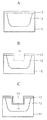
図1及び図2は化学気相蒸着方法にてタングステン膜を形成する方法を示している。
【0004】
図1Aを参照すると、シリコン基板上10にイオンを注入してソース/ドレイン領域になる不純物領域12を形成する。次いで、不純物領域12の形成された基板10の全面に、絶縁膜13としてシリコン酸化膜を500〜2000Åの厚さで形成する。次に、図1Bのように前記絶縁膜13とシリコン基板10を所定の深さで蝕刻して金属配線の形成されるトレンチ19を形成する。
【0005】
次いで、前記絶縁膜13の上部及びトレンチ19の内部にチタン(Ti)膜を200〜1500Åの厚さで蒸着した後、熱処理を行う。熱処理によりシリコン基板10とチタン膜とが反応して、基板との接触面のみにオーミック(ohmic) 層として作用するチタンシリサイド(TiSix)14 が形成される。次に、反応しないチタンの残留物を湿式蝕刻工程を用い取り除いて図1Cのような結果物を得る。
【0006】
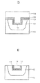
次に、図2Dのように拡散防止膜15としてチタン窒化膜(TiN) を150〜900Åの厚さで蒸着した後、その上にタングステン膜16を1000Å以上の厚さで蒸着する。
【0007】
その後、化学機械ポリシング(chemical mechanical polishing:以下、CMPという) 等の方法にてエッチバックして、図2Eのようにトレンチ19内のみにタングステン膜16を残して金属配線を完成させる。
【0008】
ところが、前述したように、選択的タングステン化学気相蒸着工程を用いて金属配線を形成する場合には、拡散防止膜のチタン窒化膜と金属配線膜のタングステン膜の物理的な特性(例えば、引っ張り力)が異なるために、両膜の界面におけるストレスが大きくなる。従って、タングステン膜がリフティングされる問題点が発生し、特に物理的な力を与えるCMP工程の適用時にチタン窒化膜/タングステン膜が絶縁膜からリフティングされ得る。
【0009】
一方、前記不純物領域をP+不純物のホウ素(B) にて形成する場合、後続熱処理工程時不純物がチタンと反応してTiB2を形成する。従って、オーミックコンタクト特性を低下させ、コンタクト抵抗を高める問題が発生する。
【0010】
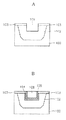
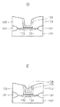
前記のような問題点を解決するために、図3Aのようにシリコン基板20上に形成された不純物領域22上にオーミック層としてタングステン膜24、拡散防止膜としてタングステン窒化膜25を形成した後、金属配線膜としてタングステン膜26を形成する方法が提案された。
【0011】
前記方法に応じて、蒸着温度600℃、圧力0.1Torr 下でタングステンフッ化物(WF6) を6sccmに、水素(H2)を200sccmのフロー率でフローさせて200〜1500Åの厚さでオーミック層のタングステン膜24を形成した後、150〜900Åの厚さで拡散防止膜のタングステン窒化膜25を蒸着してから、その上にタングステン膜26を1000Å以上の厚さで蒸着する。次に、結果物をエッチバックして金属配線を完成する。金属配線の断面を走査電子顕微鏡にて撮影した写真が図3Bに示されている。
【0012】
ところが、オーミック層としてタングステン膜を形成する場合には、シリコンとの接着特性に優れる反面、タングステンシリサイドを形成するためのタングステンとシリコンとの還元反応により、図3Bに示されたようにシリコン基板が侵蝕されて電気的な特性が劣化される更に他の問題点が発生する。侵蝕の問題は接合の深さ(junction depth)が0.1μm以下に浅くなる超高集積(ULSI)時代には尚更深刻な問題を引き起こす。かつ、タングステンとシリコンが550℃以上で反応するために、後続工程が前記温度より高い温度で行われる場合には、前記金属配線製造方法を半導体製造工程に適用することが困難である。
【0013】
【発明が解決しょうとする課題】
本発明の目的は前述した従来の問題点を解決するための半導体装置の製造方法を提供することである。
【0014】
【課題を解決するための手段】
前記目的を達成するために本発明の半導体装置は、導電層の形成されている半導体基板上に絶縁膜を形成する段階と、前記絶縁膜を蝕刻して前記導電層を露出させるコンタクトホールを形成する段階と、前記露出される導電層上にチタンシリサイド膜を形成することによりオーミック層を形成する段階と、窒素系ガス、タングステンソースガス、還元剤ガスの混合ガスを注入して前記コンタクトホールの内部のみに選択的にタングステン窒化膜を蒸着する段階とを具備することを特徴とする。
【0015】
かつ、前記目的を達成するために本発明による半導体装置の金属配線は、導電層の形成された半導体基板上に絶縁膜を形成する段階と、前記絶縁膜を蝕刻して前記導電層を露出させるコンタクトホールを形成する段階と、前記コンタクトホールにより露出された導電層上にタングステン窒化膜を蒸着する段階と、前記タングステン窒化膜の形成された結果物を熱処理してタングステン窒化膜内のタングステンがシリコン基板と反応して薄いタングステンシリサイド膜からなるオーミック層を形成させる段階と、イン−シーツ(in situ)方法にて窒素系ガス、タングステンソースガス及び、還元剤ガスの混合ガスを注入して、前記オーミック層上にタングステン窒化膜を連続的に蒸着して拡散防止膜を形成する段階と、前記拡散防止膜上に金属膜を蒸着する段階とを具備することを特徴とする。
【0016】
本発明において、前記タングステンソースガスはWF6 又はWCl6を、前記窒素系ガスはN2,NH3又はメチル-ハイドライジンを、前記還元剤ガスはH2,SiH4,SiH2Cl2又はPH3を用いることが望ましい。
【0017】
かつ、前記窒素系ガス:タングステンソースガスのフロー率の比は0.5 乃至100であることが望ましく、2乃至7は更に望ましい。そして、前記還元剤ガス:タングステンソースガスのフロー率の比は0乃至500であることが望ましく、20乃至50は更に望ましい。
【0019】
本発明によると、シリコン基板又は下部金属配線を露出させるコンタクトホール内部のみに選択的にタングステン窒化膜を形成することができるので、信頼度の高い金属配線を形成することができる。
【0020】
【発明の実施の形態】
以下、本発明の実施例を添付した図面に基づき更に詳細に説明する。
【0021】
タングステン窒化膜の成長装置
図4は本発明によるタングステン窒化膜を蒸着するための化学気相蒸着(CVD) 反応室の断面図である。
【0022】
図4を参照すると、ウェーハをローディングするためのサセプタ(susceptor) 30が反応室40の下部に設けられている。上部にはウェーハ32の温度を反応に適した温度に上昇させる役割を果たすIRランプ39が設けられている。タングステンソースガスと窒素系ガスは第1ガス注入口34を通して注入され、サセプタ30上にローディングされるウェーハ32に水平にフローされる。還元剤ガスは第2ガス注入口36を通して注入された後、メッシュノズル38を通してウェーハ32に垂直にフローされて、第1ガス注入口34から注入されるガスと反応してウェーハ32上にタングステン窒化膜を形成する。そして、第1及び第2ガス注入口34,36 と反対側に形成されている排出口42を通して反応の完了したガスが外部に排出される。
【0023】
タングステン窒化膜の製造
前記反応室40内の真空度を10-6Torr以下に設定して、反応室内で発生され得る汚染源を最少化する。次に、前記サセプタ30上に不純物領域の形成されたシリコン基板又はアルミニウム(Al)、タングステン(W) 、モリブデン(Mo)、コバルト(Co)、チタン(Ti)、銅(Cu)、白金(Pt)等のような純粋金属、それらのシリサイド化合物及びそれらの合金からなる群から選択された何れか一つから構成された下部金属配線膜の形成されたシリコン基板をローディングする。反応室40内の温度をIRランプ39により200〜700℃まで上昇させた後、第1及び第2ガス注入口34,36 を通して反応ガスを注入する。前記反応ガスは0.01 〜1Torrの圧力で注入することが望ましい。この際、第1ガス注入口34に注入されるタングステンソースガスとしてはWF6 又はWCl6を、前記窒素系ガスとしてはN2,NH3 又はメチル-ハイドライジンを用いることが望ましい。かつ、第2ガス注入口36に注入される還元剤ガスとしてはH2,SiH4,SiH2Cl2又はPH3のうち選択された何れか一つのガスを用いることが望ましい。窒素系ガス:タングステンソースガスのフロー率の比は0.5 乃至100であることが望ましく、2乃至7は更に望ましい。そして、還元剤ガス:タングステンソースガスのフロー率の比は0乃至500であることが望ましく、20乃至50は更に望ましい。
【0024】
図5及び図6にはNH3ガス とタングステンソースガスとのフロー比に応じて変化するタングステン窒化膜の成長を示す走査電子顕微鏡(SEM) の断面写真が示されている。
【0025】
コンタクトホールの形成されたシリコン基板を化学気相蒸着装置の反応室(図4の40参照)にローディングした後、蒸着温度600℃、圧力0.1Torr、WF6フロー率6sccm、N2フロー率200sccmに工程条件を工程させて、NH3フロー率 を0,10,20,40sccm にそれぞれ異なるようにしてタングステン窒化膜を形成した後、その結果を測定したSEM写真を図5A乃至図6Dにそれぞれ示した。
【0026】
コンタクトホール内に純粋タングステン膜だけが形成された図5Aの写真を見ると、従来技術の問題点で説明したように、基板の侵蝕現象が大変深刻なことが分かる。その反面、NH3フロー率 を10sccmにした場合には、図5Bのように侵蝕現象が抑制されたものの、薄膜はほとんど成長せず、コンタクトホールの底部の表面だけに核が形成された。NH3フロー率 を20sccmにした場合には、図6Cのようにタングステン窒化膜がコンタクトホール内の基板部分と側壁だけで選択的に成長され、コンタクトホール以外のシリコン酸化膜上では成長しなかった。ところが、図6DのようにNH3フロー率 を40sccmに増加した場合には、タングステン窒化膜の選択的成長特性が無くなり、基板の全面に成長する現象を示した。
【0027】
従って、窒素系ガス:タングステンソースガスのフロー率の比を調節することにより、タングステン窒化膜をコンタクトホール内でのみ選択的に成長させ得ることが分かった。このような事実は図6Cに形成されたタングステン窒化膜のX線回折分析結果を示す図7を参照すると更に明確になる。図7を見ると、結晶方向の相異なるβ-W2N位相のピークが三つ確認される。これは、シリコン基板上に選択的にタングステン窒化膜が形成されたことを示すものである。
【0028】
金属配線製造方法
前述したタングステン窒化膜の製造方法を用いて半導体装置の金属配線を形成する方法を図8乃至図11を参考して説明する。
【0029】
第1実施例
図8Aを参照すると、不純物領域102の形成されたシリコン基板100上に絶縁膜103、例えばシリコン酸化膜を500〜2000Åの厚さで形成する。この際、前記シリコン酸化膜の代りにシリコン窒化膜又はシリコン酸化膜、シリコン窒化膜に不純物を添加した膜を絶縁膜103として用いることもできる。次いで、写真蝕刻工程にて前記絶縁膜103を乾式蝕刻して不純物領域102を露出させるコンタクトホール110を形成する。
【0030】
図8Bを参照すると、前記絶縁膜103の上部及びコンタクトホール110の内部にti膜を200〜1500Åの厚さで蒸着する。次に、熱処理を行い前記コンタクトホール110により露出されたシリコン基板100と反応させて、その接触面のみにTiSix膜104 を形成する。反応しないTiの残留物は湿式蝕刻工程を用いて取り除く。前記TiSix膜104 はオーミック層として作用する。
【0031】
図8Cを参照すると、シリコン基板100の温度を200〜700℃まで上昇させ、窒素系ガス、タングステンソースガス及び還元剤ガスをフローさせて、コンタクトホール110により露出された基板100と絶縁膜103の側壁のみにタングステン窒化膜105を選択的に蒸着させる。ここで、窒素系ガス:タングステンソースガスのフロー率の比は0.5〜100 にし、還元剤ガス:タングステンソースガスのフロー率の比は0〜500にする。
【0032】
図8Dを参照すると、タングステン窒化膜105を形成した後、イン−シーツ方法にて前記コンタクトホール110の内部のみに金属薄膜108を蒸着させて金属配線を形成する。この際、前記金属膜はAl,W,Mo,Co,Ti,Cu,Pt 等の純粋金属、それらのシリサイド化合物及びそれらの合金からなる群から選択された何れか一つを用いて形成することが望ましい。
【0033】
第2実施例
第2実施例が第1実施例と異なる点は、絶縁膜を蝕刻して形成したコンタクトホール(図8Aの110参照)内に金属配線を形成せず、図9Aに示されたように絶縁膜103及び基板100を蝕刻してトレンチ109を形成した後、金属配線膜を形成することである。トレンチ109の形成後、図9Bのようにオーミック層としてTiSix膜104 、拡散防止膜としてタングステン窒化膜105を順番に形成した後、金属膜としてタングステン膜108を形成して金属配線を完成する工程は第1実施例と同一である。トレンチ109を形成する理由はコンタクトホールのアスペクト比が増加する問題を解決するためである。
【0034】
第3実施例
第3実施例が第1及び第2実施例と著しく相異なる点は、オーミック層としてチタンシリサイド膜の代りにCVD方法にてタングステン又はタングステンシリサイド等のタングステン化合物を蒸着してコンタクト抵抗を下げ、拡散防止膜のタングステン窒化膜をイン−シーツ方法にてCVD方法により蒸着するという点である。
【0035】
図10Aを参照すると、通常の素子分離工程によりシリコン基板100上に活性領域を分離させるための素子分離領域101を形成した後、イオン注入工程により不純物領域、例えばN+又はP+接合102を前記活性領域に形成する。次いで、結果物上に絶縁膜103、例えばBPSGを塗布して段差部分を平坦化させる。
【0036】
図10Bを参照すると、写真蝕刻工程により前記絶縁膜103を蝕刻してシリコン基板100の不純物領域102を露出させるコンタクトホール110を形成する。
【0037】
図10Cを参照すると、前記コンタクトホール110の形成された結果物上にCVD方法によりタングステン系統のオーミック層124を形成する。この際、前記オーミック層124は下記の四つの方法により形成され得る。
【0038】
▲1▼シリコンの侵蝕が発生しない程度の短時間にタングステンソースガスをフローさせてタングステンオーミック層124を蒸着する。
【0039】
▲2▼蒸着の初期には窒素系ガス:タングステンソースガスのフロー率の比を2以下に下げて、コンタクトホールの底部のみに浅くも豊富なタングステンを有するオーミック層124を形成してシリコン侵蝕を防止する。次に、窒素系ガスのフロー量を増加させて窒素系ガス:タングステンソースガスの割合を2〜100、更に望ましくは2〜7に調整して、コンタクトホール110内にタングステン窒化膜125を形成する。このようにすると、シリコンの侵蝕の発生も防止でき、タングステン窒化膜もコンタクトホール内のみで選択的に形成され得る。
【0040】
▲3▼タングステンソースガスにSiH4 又はSiH2Cl2ガスを混合して500℃以上で蒸着してタングステンシリサイドを形成することによりオーミック層124を形成する。
【0041】
▲4▼タングステン窒化膜の障壁金属をシリコン基板上に直接蒸着した後、タングステン窒化膜のタングステン元素がその下部のシリコンと反応してタングステンシリサイドを形成し得るように、アニールしてオーミック層124を形成する。
【0042】
図11Dを参照すると、前記オーミック層124を蒸着した同一チャンバ内で、第1実施例と同一な方法を用いて拡散防止膜125、即ちタングステン窒化膜を500Å以上の厚さになるように蒸着する。
【0043】
図11Eを参照すると、前記拡散防止膜125の形成された結果物上に金属配線膜128を蒸着する。前記金属配線膜128はアルミニウムや銅のような配線用金属を蒸着して金属配線を形成することが望ましい。
【0044】
【発明の効果】
本発明によると、絶縁膜上には蒸着させず、コンタクトホールの側壁及びコンタクトホールにより露出されたシリコン基板又は下部金属配線層のみにタングステン窒化膜を選択的に形成することができる。従って、拡散防止膜としてタングステン窒化膜を形成した後、金属配線膜としてタングステン膜を形成すると、両膜間の物理的な特性が類似であるために、従来の金属配線膜から発生したリフティング問題が解決される。そして、本発明の第3実施例に応じてオーミック層を形成すると、基板侵蝕の問題も解決され、後続の高温工程でも安定した半導体素子を形成することができる。かつ、チタン膜を用いてオーミック層を形成する時に発生したコンタクト抵抗増加の問題も解決される。
【0045】
本発明は前記実施例に限られず、多くの変形が本発明の技術的思想内で当分野において通常の知識を有する者により可能であることは明白である。
【図面の簡単な説明】
【図1】チタン/チタン窒化膜/タングステン膜からなる従来の金属配線製造方法を説明するための工程別断面図である。
【図2】図1に続く工程別断面図である。
【図3】同図Aはタングステン/タングステン窒化膜/タングステン膜からなる従来の金属配線製造方法を説明するための断面図であり、同図Bは同図Aに示された金属配線の走査電子顕微鏡断面写真である。
【図4】本発明によるタングステン窒化膜を蒸着するための反応室の断面図である。
【図5】 NH3 フロー率に応じて選択的に成長するタングステン窒化膜の断面を示す走査電子顕微鏡写真である。
【図6】図5と同様の走査電子顕微鏡写真である。
【図7】本発明により形成されたタングステン窒化膜のX線回折結果を示したグラフである。
【図8】本発明の第1実施例による半導体装置の金属配線製造方法を説明するための工程別断面図である。
【図9】本発明の第2実施例による半導体装置の金属配線製造方法を説明するための工程別断面図である。
【図10】本発明の第3実施例による半導体装置の金属配線製造方法を説明するための工程別断面図である。
【図11】図10に続く工程別断面図である。[0001]
BACKGROUND OF THE INVENTION
The present invention relates to a method of manufacturing a semiconductor device, and in particular, forms a tungsten nitride film that is selectively formed only in a contact hole or on a lower metal wiring layer without corroding a substrate or a lower wiring film, and is stable even at a high temperature. The present invention relates to a method and a metal wiring manufacturing method using the method.
[0002]
[Prior art]
As the degree of integration of semiconductor integrated circuits increases, the width of metal wiring is gradually reduced, and the aspect ratio is increasing in contact holes. However, since a metal film such as an aluminum alloy currently used as a material for metal wiring is formed by sputtering or the like, the step coating property in the contact hole is poor or a defect such as a void occurs. . As a result, disconnection or the like between the metal wirings is caused and the reliability of the integrated circuit is lowered. Accordingly, a selective tungsten chemical vapor deposition method (hereinafter referred to as SCVD-W) in which metal wiring is formed using tungsten that can be deposited by a chemical vapor deposition method has attracted attention.
[0003]
1 and 2 show a method of forming a tungsten film by a chemical vapor deposition method.
[0004]
Referring to FIG. 1A, ions are implanted into a
[0005]
Next, a titanium (Ti) film is deposited on the
[0006]
Next, as shown in FIG. 2D, after a titanium nitride film (TiN) is deposited as a
[0007]
Thereafter, etching back is performed by a method such as chemical mechanical polishing (hereinafter referred to as CMP) to complete the metal wiring by leaving the
[0008]
However, as described above, when the metal wiring is formed using the selective tungsten chemical vapor deposition process, the physical characteristics of the titanium nitride film of the diffusion prevention film and the tungsten film of the metal wiring film (for example, tensile Stress) at the interface between the two films increases. Therefore, there is a problem that the tungsten film is lifted, and the titanium nitride film / tungsten film can be lifted from the insulating film particularly when a CMP process that applies physical force is applied.
[0009]
On the other hand, when the impurity region is formed of P + impurity boron (B), the impurity reacts with titanium in the subsequent heat treatment step to form TiB 2 . Accordingly, there arises a problem that the ohmic contact characteristics are deteriorated and the contact resistance is increased.
[0010]
In order to solve the above problems, after forming a
[0011]
In accordance with the above method, tungsten fluoride (WF 6 ) was flowed to 6 sccm and hydrogen (H 2 ) at a flow rate of 200 sccm at a deposition temperature of 600 ° C. and a pressure of 0.1 Torr, and ohmic with a thickness of 200 to 1500 mm. After forming the
[0012]
However, when a tungsten film is formed as an ohmic layer, the silicon substrate is excellent in adhesion characteristics with silicon, but the silicon substrate is formed as shown in FIG. 3B by the reduction reaction between tungsten and silicon for forming tungsten silicide. Yet another problem occurs in which the electrical characteristics are deteriorated by being eroded. The problem of erosion causes even more serious problems in the ultra-high integration (ULSI) era when the junction depth is shallower than 0.1 μm. In addition, since tungsten and silicon react at 550 ° C. or higher, it is difficult to apply the metal wiring manufacturing method to a semiconductor manufacturing process when the subsequent process is performed at a temperature higher than the temperature.
[0013]
[Problems to be solved by the invention]
An object of the present invention is to provide a semiconductor device manufacturing method for solving the above-described conventional problems.
[0014]
[Means for Solving the Problems]
In order to achieve the above object, a semiconductor device according to the present invention includes a step of forming an insulating film on a semiconductor substrate on which a conductive layer is formed, and a contact hole that exposes the conductive layer by etching the insulating film. Forming an ohmic layer by forming a titanium silicide film on the exposed conductive layer, and injecting a mixed gas of a nitrogen-based gas, a tungsten source gas, and a reducing agent gas to form the contact hole. And depositing a tungsten nitride film selectively only inside.
[0015]
In order to achieve the above object, the metal wiring of the semiconductor device according to the present invention includes a step of forming an insulating film on a semiconductor substrate on which a conductive layer is formed, and etching the insulating film to expose the conductive layer. Forming a contact hole; depositing a tungsten nitride film on the conductive layer exposed by the contact hole; and heat-treating the resultant tungsten nitride film to form tungsten in the silicon nitride film. A step of forming an ohmic layer comprising a thin tungsten silicide film by reacting with a substrate, and injecting a mixed gas of a nitrogen-based gas, a tungsten source gas, and a reducing agent gas by an in-situ method; Forming a diffusion barrier film by continuously depositing a tungsten nitride film on the ohmic layer; and And evaporating a metal film.
[0016]
In the present invention, the tungsten source gas is WF 6 or WCl 6 , the nitrogen-based gas is N 2 , NH 3 or methyl-hydridine, and the reducing agent gas is H 2 , SiH 4 , SiH 2 Cl 2 or PH. It is desirable to use 3 .
[0017]
The flow rate ratio of the nitrogen-based gas: tungsten source gas is preferably 0.5 to 100, more preferably 2 to 7. The flow rate ratio of the reducing agent gas: tungsten source gas is preferably 0 to 500, more preferably 20 to 50.
[0019]
According to the present invention, since the tungsten nitride film can be selectively formed only inside the contact hole exposing the silicon substrate or the lower metal wiring, a highly reliable metal wiring can be formed.
[0020]
DETAILED DESCRIPTION OF THE INVENTION
Hereinafter, embodiments of the present invention will be described in more detail with reference to the accompanying drawings.
[0021]
Growth apparatus <br/> Figure 4 of the tungsten nitride film is a cross-sectional view of a chemical vapor deposition (CVD) reaction chamber for depositing a tungsten nitride film according to the present invention.
[0022]
Referring to FIG. 4, a
[0023]
Production of tungsten nitride film The degree of vacuum in the
[0024]
FIGS. 5 and 6 show cross-sectional photographs of a scanning electron microscope (SEM) showing the growth of a tungsten nitride film that changes depending on the flow ratio of NH 3 gas and tungsten source gas.
[0025]
After loading the silicon substrate with contact holes into the reaction chamber of the chemical vapor deposition apparatus (see 40 in FIG. 4), the deposition temperature is 600 ° C., the pressure is 0.1 Torr, the WF 6 flow rate is 6 sccm, and the N 2 flow rate is 200 sccm. 5A to 6D show SEM photographs in which the tungsten nitride film was formed with different NH 3 flow rates of 0, 10, 20, and 40 sccm, and the results were measured. It was.
[0026]
When the photograph of FIG. 5A in which only the pure tungsten film is formed in the contact hole is seen, the substrate erosion phenomenon is very serious as described in the problem of the prior art. On the other hand, when the NH 3 flow rate was 10 sccm, the erosion phenomenon was suppressed as shown in FIG. 5B, but the thin film hardly grew and nuclei were formed only on the bottom surface of the contact hole. When the NH 3 flow rate was 20 sccm, the tungsten nitride film was selectively grown only on the substrate portion and the side wall in the contact hole as shown in FIG. 6C, and did not grow on the silicon oxide film other than the contact hole. . However, when the NH 3 flow rate was increased to 40 sccm as shown in FIG. 6D, the selective growth characteristic of the tungsten nitride film disappeared and the phenomenon of growing on the entire surface of the substrate was shown.
[0027]
Therefore, it was found that the tungsten nitride film can be selectively grown only in the contact hole by adjusting the flow rate ratio of nitrogen-based gas: tungsten source gas. Such a fact becomes clearer with reference to FIG. 7 showing the result of X-ray diffraction analysis of the tungsten nitride film formed in FIG. 6C. FIG. 7 shows three β-W 2 N phase peaks with different crystal directions. This indicates that a tungsten nitride film is selectively formed on the silicon substrate.
[0028]
Metal wiring manufacturing method A method of forming a metal wiring of a semiconductor device using the above-described tungsten nitride film manufacturing method will be described with reference to FIGS.
[0029]
First embodiment Referring to FIG. 8A, an insulating
[0030]
Referring to FIG. 8B, a ti film is deposited to a thickness of 200 to 1500 mm on the insulating
[0031]
Referring to FIG. 8C, the temperature of the
[0032]
Referring to FIG. 8D, after the
[0033]
Second embodiment The second embodiment is different from the first embodiment in that no metal wiring is formed in a contact hole (see 110 in FIG. 8A) formed by etching an insulating film. The metal film is formed after the
[0034]
Third embodiment The third embodiment is significantly different from the first and second embodiments in that a tungsten compound such as tungsten or tungsten silicide is deposited by CVD instead of a titanium silicide film as an ohmic layer. Then, the contact resistance is lowered, and a tungsten nitride film as a diffusion preventing film is deposited by a CVD method by an in-sheet method.
[0035]
Referring to FIG. 10A, after forming an
[0036]
Referring to FIG. 10B, the insulating
[0037]
Referring to FIG. 10C, a tungsten-based
[0038]
{Circle around (1)} A
[0039]
(2) At the initial stage of deposition, the flow rate ratio of nitrogen-based gas: tungsten source gas is lowered to 2 or less to form an
[0040]
(3) The
[0041]
(4) After the barrier metal of the tungsten nitride film is directly deposited on the silicon substrate, the
[0042]
Referring to FIG. 11D, in the same chamber in which the
[0043]
Referring to FIG. 11E, a
[0044]
【The invention's effect】
According to the present invention, the tungsten nitride film can be selectively formed only on the side wall of the contact hole and the silicon substrate or the lower metal wiring layer exposed by the contact hole without being deposited on the insulating film. Therefore, when a tungsten nitride film is formed as a metal wiring film after a tungsten nitride film is formed as a diffusion prevention film, the physical characteristics between the two films are similar. Solved. If the ohmic layer is formed according to the third embodiment of the present invention, the problem of substrate erosion can be solved, and a stable semiconductor device can be formed even in the subsequent high-temperature process. In addition, the problem of increased contact resistance that occurs when an ohmic layer is formed using a titanium film is also solved.
[0045]
The present invention is not limited to the above-described embodiments, and it is obvious that many modifications can be made by those having ordinary knowledge in the art within the technical idea of the present invention.
[Brief description of the drawings]
FIG. 1 is a cross-sectional view by process for explaining a conventional metal wiring manufacturing method comprising a titanium / titanium nitride film / tungsten film.
FIG. 2 is a sectional view by process following FIG. 1;
3A is a cross-sectional view for explaining a conventional method for manufacturing a metal wiring composed of tungsten / tungsten nitride film / tungsten film, and FIG. 3B is a scanning electron of the metal wiring shown in FIG. It is a microscope cross-sectional photograph.
FIG. 4 is a cross-sectional view of a reaction chamber for depositing a tungsten nitride film according to the present invention.
FIG. 5 is a scanning electron micrograph showing a cross section of a tungsten nitride film selectively grown according to the NH 3 flow rate.
6 is a scanning electron micrograph similar to FIG.
FIG. 7 is a graph showing an X-ray diffraction result of a tungsten nitride film formed according to the present invention.
FIG. 8 is a cross-sectional view for explaining a method for manufacturing a metal wiring of a semiconductor device according to the first embodiment of the present invention.
FIG. 9 is a cross-sectional view for explaining a method of manufacturing a metal wiring of a semiconductor device according to a second embodiment of the present invention.
FIG. 10 is a cross-sectional view for explaining a method of manufacturing a metal wiring of a semiconductor device according to a third embodiment of the present invention.
FIG. 11 is a cross-sectional view by process following FIG. 10;
Claims (24)
前記絶縁膜を蝕刻して前記導電層を露出させるコンタクトホールを形成する段階と、
前記露出される導電層上にチタンシリサイド膜を形成することによりオーミック層を形成する段階と、
窒素系ガス、タングステンソースガス及び還元剤ガスの混合ガスを注入して前記コンタクトホールの内部のみに選択的にタングステン窒化膜を蒸着する段階とを具備することを特徴とするタングステン窒化膜の製造方法。Forming an insulating film on the semiconductor substrate on which the conductive layer is formed;
Etching the insulating film to form a contact hole exposing the conductive layer;
Forming an ohmic layer by forming a titanium silicide film on the exposed conductive layer;
Injecting a mixed gas of a nitrogen-based gas, a tungsten source gas and a reducing agent gas, and selectively depositing a tungsten nitride film only inside the contact hole. .
前記絶縁膜を蝕刻して前記導電層を露出させるコンタクトホールを形成する段階と、
前記コンタクトホールにより露出された導電層上にタングステン窒化膜を蒸着する段階と、
前記タングステン窒化膜の形成された結果物を熱処理してタングステン窒化膜内のタングステンがシリコン基板と反応して薄いタングステンシリサイド膜からなるオーミック層を形成させる段階と、
イン−シーツ方法にて窒素系ガス、タングステンソースガス及び還元剤ガスの混合ガスを注入して、前記オーミック層上にタングステン窒化膜を連続的に蒸着して拡散防止膜を形成する段階と、
前記拡散防止膜上に金属膜を蒸着する段階とを具備することを特徴とする半導体装置の金属配線製造方法。Forming an insulating film on the semiconductor substrate on which the conductive layer is formed;
Etching the insulating film to form a contact hole exposing the conductive layer;
Depositing a tungsten nitride film on the conductive layer exposed by the contact hole;
Heat-treating the resultant structure having the tungsten nitride film so that tungsten in the tungsten nitride film reacts with the silicon substrate to form an ohmic layer made of a thin tungsten silicide film;
Injecting a mixed gas of a nitrogen-based gas, a tungsten source gas and a reducing agent gas by an in-sheet method, and continuously depositing a tungsten nitride film on the ohmic layer to form a diffusion prevention film;
Depositing a metal film on the diffusion barrier film. A method of manufacturing a metal wiring of a semiconductor device.
Priority Applications (1)
| Application Number | Priority Date | Filing Date | Title |
|---|---|---|---|
| JP32914896A JP3868043B2 (en) | 1996-11-25 | 1996-11-25 | Tungsten nitride film manufacturing method and metal wiring manufacturing method using the same |
Applications Claiming Priority (1)
| Application Number | Priority Date | Filing Date | Title |
|---|---|---|---|
| JP32914896A JP3868043B2 (en) | 1996-11-25 | 1996-11-25 | Tungsten nitride film manufacturing method and metal wiring manufacturing method using the same |
Publications (2)
| Publication Number | Publication Date |
|---|---|
| JPH10163128A JPH10163128A (en) | 1998-06-19 |
| JP3868043B2 true JP3868043B2 (en) | 2007-01-17 |
Family
ID=18218186
Family Applications (1)
| Application Number | Title | Priority Date | Filing Date |
|---|---|---|---|
| JP32914896A Expired - Fee Related JP3868043B2 (en) | 1996-11-25 | 1996-11-25 | Tungsten nitride film manufacturing method and metal wiring manufacturing method using the same |
Country Status (1)
| Country | Link |
|---|---|
| JP (1) | JP3868043B2 (en) |
Families Citing this family (1)
| Publication number | Priority date | Publication date | Assignee | Title |
|---|---|---|---|---|
| US7605429B2 (en) * | 2005-04-15 | 2009-10-20 | International Business Machines Corporation | Hybrid crystal orientation CMOS structure for adaptive well biasing and for power and performance enhancement |
-
1996
- 1996-11-25 JP JP32914896A patent/JP3868043B2/en not_active Expired - Fee Related
Also Published As
| Publication number | Publication date |
|---|---|
| JPH10163128A (en) | 1998-06-19 |
Similar Documents
| Publication | Publication Date | Title |
|---|---|---|
| EP0841690A1 (en) | Tungsten nitride (WNx) layer manufacturing method and metal wiring manufacturing method | |
| US6903462B2 (en) | Chemical vapor deposition of titanium | |
| US5652180A (en) | Method of manufacturing semiconductor device with contact structure | |
| US20010006240A1 (en) | Method of forming titanium silicide and titanium by chemical vapor deposition and resulting apparatus | |
| JP3221381B2 (en) | Method for manufacturing semiconductor device | |
| WO2002067319A2 (en) | Copper interconnect structure having diffusion barrier | |
| JP3175721B2 (en) | Method for manufacturing semiconductor device | |
| JPH08274043A (en) | Method for manufacturing semiconductor device | |
| JP2000306997A (en) | Semiconductor device having barrier metal layer and method of manufacturing the same | |
| US6509254B1 (en) | Method of forming electrode structure and method of fabricating semiconductor device | |
| CN1115723C (en) | Tungsten nitride (WNx) layer manufacturing method and metal wiring manufacturing method using the same | |
| US6777330B2 (en) | Chemistry for chemical vapor deposition of titanium containing films | |
| EP0420589A2 (en) | Process for forming deposited film and process for preparing semiconductor device | |
| US6433434B1 (en) | Apparatus having a titanium alloy layer | |
| JPH05129231A (en) | Electrode wiring | |
| JPH06204170A (en) | Semiconductor device and manufacturing method thereof | |
| JP3868043B2 (en) | Tungsten nitride film manufacturing method and metal wiring manufacturing method using the same | |
| JPH1167688A (en) | Silicide material, its thin-film and manufacture of silicide thin-film | |
| JP3072544B2 (en) | Semiconductor device wiring method | |
| KR0175016B1 (en) | Selective tungsten nitride thin film formation method and metallization method using the same | |
| KR100609049B1 (en) | Metal wiring formation method of semiconductor device | |
| JPH09102469A (en) | Manufacture of semiconductor device | |
| KR0150989B1 (en) | Semiconductor Device Wiring Formation Method | |
| JP3085745B2 (en) | Method for manufacturing semiconductor device | |
| JPH0629241A (en) | Manufacture of semiconductor device |
Legal Events
| Date | Code | Title | Description |
|---|---|---|---|
| A977 | Report on retrieval |
Free format text: JAPANESE INTERMEDIATE CODE: A971007 Effective date: 20050907 |
|
| A131 | Notification of reasons for refusal |
Free format text: JAPANESE INTERMEDIATE CODE: A131 Effective date: 20060606 |
|
| A521 | Written amendment |
Free format text: JAPANESE INTERMEDIATE CODE: A523 Effective date: 20060831 |
|
| TRDD | Decision of grant or rejection written | ||
| A01 | Written decision to grant a patent or to grant a registration (utility model) |
Free format text: JAPANESE INTERMEDIATE CODE: A01 Effective date: 20060926 |
|
| A61 | First payment of annual fees (during grant procedure) |
Free format text: JAPANESE INTERMEDIATE CODE: A61 Effective date: 20061010 |
|
| R150 | Certificate of patent or registration of utility model |
Free format text: JAPANESE INTERMEDIATE CODE: R150 |
|
| FPAY | Renewal fee payment (event date is renewal date of database) |
Free format text: PAYMENT UNTIL: 20091020 Year of fee payment: 3 |
|
| FPAY | Renewal fee payment (event date is renewal date of database) |
Free format text: PAYMENT UNTIL: 20101020 Year of fee payment: 4 |
|
| FPAY | Renewal fee payment (event date is renewal date of database) |
Free format text: PAYMENT UNTIL: 20111020 Year of fee payment: 5 |
|
| FPAY | Renewal fee payment (event date is renewal date of database) |
Free format text: PAYMENT UNTIL: 20121020 Year of fee payment: 6 |
|
| LAPS | Cancellation because of no payment of annual fees |