JP3856901B2 - Display device - Google Patents
Display device Download PDFInfo
- Publication number
- JP3856901B2 JP3856901B2 JP11354997A JP11354997A JP3856901B2 JP 3856901 B2 JP3856901 B2 JP 3856901B2 JP 11354997 A JP11354997 A JP 11354997A JP 11354997 A JP11354997 A JP 11354997A JP 3856901 B2 JP3856901 B2 JP 3856901B2
- Authority
- JP
- Japan
- Prior art keywords
- electrode
- display device
- insulating film
- circuit
- film
- Prior art date
- Legal status (The legal status is an assumption and is not a legal conclusion. Google has not performed a legal analysis and makes no representation as to the accuracy of the status listed.)
- Expired - Fee Related
Links
- 239000010408 film Substances 0.000 claims description 140
- 230000002093 peripheral effect Effects 0.000 claims description 49
- RTAQQCXQSZGOHL-UHFFFAOYSA-N Titanium Chemical compound [Ti] RTAQQCXQSZGOHL-UHFFFAOYSA-N 0.000 claims description 37
- 239000010936 titanium Substances 0.000 claims description 37
- 229910052719 titanium Inorganic materials 0.000 claims description 37
- 239000004973 liquid crystal related substance Substances 0.000 claims description 35
- 239000000758 substrate Substances 0.000 claims description 34
- 239000011159 matrix material Substances 0.000 claims description 33
- 229910052782 aluminium Inorganic materials 0.000 claims description 30
- XAGFODPZIPBFFR-UHFFFAOYSA-N aluminium Chemical compound [Al] XAGFODPZIPBFFR-UHFFFAOYSA-N 0.000 claims description 30
- 239000000463 material Substances 0.000 claims description 20
- 239000010410 layer Substances 0.000 claims description 18
- 239000010409 thin film Substances 0.000 claims description 16
- VYPSYNLAJGMNEJ-UHFFFAOYSA-N Silicium dioxide Chemical compound O=[Si]=O VYPSYNLAJGMNEJ-UHFFFAOYSA-N 0.000 claims description 10
- 229920001721 polyimide Polymers 0.000 claims description 10
- 229910052581 Si3N4 Inorganic materials 0.000 claims description 9
- HQVNEWCFYHHQES-UHFFFAOYSA-N silicon nitride Chemical compound N12[Si]34N5[Si]62N3[Si]51N64 HQVNEWCFYHHQES-UHFFFAOYSA-N 0.000 claims description 9
- 239000003566 sealing material Substances 0.000 claims description 5
- 229910052814 silicon oxide Inorganic materials 0.000 claims description 5
- 239000004642 Polyimide Substances 0.000 claims description 4
- 239000011347 resin Substances 0.000 claims description 4
- 229920005989 resin Polymers 0.000 claims description 4
- 229910052710 silicon Inorganic materials 0.000 claims description 4
- 239000010703 silicon Substances 0.000 claims description 4
- 239000007769 metal material Substances 0.000 claims description 3
- 239000004593 Epoxy Substances 0.000 claims description 2
- 239000004952 Polyamide Substances 0.000 claims description 2
- NIXOWILDQLNWCW-UHFFFAOYSA-N acrylic acid group Chemical group C(C=C)(=O)O NIXOWILDQLNWCW-UHFFFAOYSA-N 0.000 claims description 2
- 150000001408 amides Chemical class 0.000 claims description 2
- 230000010355 oscillation Effects 0.000 claims description 2
- 229920002647 polyamide Polymers 0.000 claims description 2
- 229910021332 silicide Inorganic materials 0.000 claims description 2
- FVBUAEGBCNSCDD-UHFFFAOYSA-N silicide(4-) Chemical compound [Si-4] FVBUAEGBCNSCDD-UHFFFAOYSA-N 0.000 claims 1
- 238000004519 manufacturing process Methods 0.000 description 13
- 230000006870 function Effects 0.000 description 8
- 239000011521 glass Substances 0.000 description 6
- 230000010287 polarization Effects 0.000 description 6
- 239000009719 polyimide resin Substances 0.000 description 6
- 238000000059 patterning Methods 0.000 description 5
- 239000010453 quartz Substances 0.000 description 5
- 238000004544 sputter deposition Methods 0.000 description 5
- XUIMIQQOPSSXEZ-UHFFFAOYSA-N Silicon Chemical compound [Si] XUIMIQQOPSSXEZ-UHFFFAOYSA-N 0.000 description 3
- 238000000034 method Methods 0.000 description 3
- 238000005268 plasma chemical vapour deposition Methods 0.000 description 3
- OAICVXFJPJFONN-UHFFFAOYSA-N Phosphorus Chemical compound [P] OAICVXFJPJFONN-UHFFFAOYSA-N 0.000 description 2
- 229910021417 amorphous silicon Inorganic materials 0.000 description 2
- 239000010407 anodic oxide Substances 0.000 description 2
- 230000015572 biosynthetic process Effects 0.000 description 2
- 239000003990 capacitor Substances 0.000 description 2
- 229910021419 crystalline silicon Inorganic materials 0.000 description 2
- 238000010586 diagram Methods 0.000 description 2
- 239000012535 impurity Substances 0.000 description 2
- 239000011229 interlayer Substances 0.000 description 2
- 150000002500 ions Chemical class 0.000 description 2
- 230000003287 optical effect Effects 0.000 description 2
- 229910052698 phosphorus Inorganic materials 0.000 description 2
- 239000011574 phosphorus Substances 0.000 description 2
- 239000004065 semiconductor Substances 0.000 description 2
- ZOXJGFHDIHLPTG-UHFFFAOYSA-N Boron Chemical compound [B] ZOXJGFHDIHLPTG-UHFFFAOYSA-N 0.000 description 1
- 229910052796 boron Inorganic materials 0.000 description 1
- 238000002425 crystallisation Methods 0.000 description 1
- 239000002019 doping agent Substances 0.000 description 1
- 230000000694 effects Effects 0.000 description 1
- 238000000635 electron micrograph Methods 0.000 description 1
- 238000005516 engineering process Methods 0.000 description 1
- 238000010438 heat treatment Methods 0.000 description 1
- 230000002452 interceptive effect Effects 0.000 description 1
- 238000004518 low pressure chemical vapour deposition Methods 0.000 description 1
- 238000005259 measurement Methods 0.000 description 1
- 229910052751 metal Inorganic materials 0.000 description 1
- 239000002184 metal Substances 0.000 description 1
- 239000002052 molecular layer Substances 0.000 description 1
- 238000002310 reflectometry Methods 0.000 description 1
- 238000007789 sealing Methods 0.000 description 1
- 239000002210 silicon-based material Substances 0.000 description 1
Images


Classifications
-
- G—PHYSICS
- G02—OPTICS
- G02B—OPTICAL ELEMENTS, SYSTEMS OR APPARATUS
- G02B27/00—Optical systems or apparatus not provided for by any of the groups G02B1/00 - G02B26/00, G02B30/00
- G02B27/01—Head-up displays
- G02B27/017—Head mounted
-
- G—PHYSICS
- G02—OPTICS
- G02F—OPTICAL DEVICES OR ARRANGEMENTS FOR THE CONTROL OF LIGHT BY MODIFICATION OF THE OPTICAL PROPERTIES OF THE MEDIA OF THE ELEMENTS INVOLVED THEREIN; NON-LINEAR OPTICS; FREQUENCY-CHANGING OF LIGHT; OPTICAL LOGIC ELEMENTS; OPTICAL ANALOGUE/DIGITAL CONVERTERS
- G02F1/00—Devices or arrangements for the control of the intensity, colour, phase, polarisation or direction of light arriving from an independent light source, e.g. switching, gating or modulating; Non-linear optics
- G02F1/01—Devices or arrangements for the control of the intensity, colour, phase, polarisation or direction of light arriving from an independent light source, e.g. switching, gating or modulating; Non-linear optics for the control of the intensity, phase, polarisation or colour
- G02F1/13—Devices or arrangements for the control of the intensity, colour, phase, polarisation or direction of light arriving from an independent light source, e.g. switching, gating or modulating; Non-linear optics for the control of the intensity, phase, polarisation or colour based on liquid crystals, e.g. single liquid crystal display cells
- G02F1/133—Constructional arrangements; Operation of liquid crystal cells; Circuit arrangements
- G02F1/136—Liquid crystal cells structurally associated with a semi-conducting layer or substrate, e.g. cells forming part of an integrated circuit
- G02F1/1362—Active matrix addressed cells
- G02F1/1368—Active matrix addressed cells in which the switching element is a three-electrode device
-
- G—PHYSICS
- G02—OPTICS
- G02F—OPTICAL DEVICES OR ARRANGEMENTS FOR THE CONTROL OF LIGHT BY MODIFICATION OF THE OPTICAL PROPERTIES OF THE MEDIA OF THE ELEMENTS INVOLVED THEREIN; NON-LINEAR OPTICS; FREQUENCY-CHANGING OF LIGHT; OPTICAL LOGIC ELEMENTS; OPTICAL ANALOGUE/DIGITAL CONVERTERS
- G02F1/00—Devices or arrangements for the control of the intensity, colour, phase, polarisation or direction of light arriving from an independent light source, e.g. switching, gating or modulating; Non-linear optics
- G02F1/01—Devices or arrangements for the control of the intensity, colour, phase, polarisation or direction of light arriving from an independent light source, e.g. switching, gating or modulating; Non-linear optics for the control of the intensity, phase, polarisation or colour
- G02F1/13—Devices or arrangements for the control of the intensity, colour, phase, polarisation or direction of light arriving from an independent light source, e.g. switching, gating or modulating; Non-linear optics for the control of the intensity, phase, polarisation or colour based on liquid crystals, e.g. single liquid crystal display cells
- G02F1/133—Constructional arrangements; Operation of liquid crystal cells; Circuit arrangements
- G02F1/1333—Constructional arrangements; Manufacturing methods
- G02F1/1335—Structural association of cells with optical devices, e.g. polarisers or reflectors
- G02F1/133553—Reflecting elements
-
- G—PHYSICS
- G02—OPTICS
- G02F—OPTICAL DEVICES OR ARRANGEMENTS FOR THE CONTROL OF LIGHT BY MODIFICATION OF THE OPTICAL PROPERTIES OF THE MEDIA OF THE ELEMENTS INVOLVED THEREIN; NON-LINEAR OPTICS; FREQUENCY-CHANGING OF LIGHT; OPTICAL LOGIC ELEMENTS; OPTICAL ANALOGUE/DIGITAL CONVERTERS
- G02F1/00—Devices or arrangements for the control of the intensity, colour, phase, polarisation or direction of light arriving from an independent light source, e.g. switching, gating or modulating; Non-linear optics
- G02F1/01—Devices or arrangements for the control of the intensity, colour, phase, polarisation or direction of light arriving from an independent light source, e.g. switching, gating or modulating; Non-linear optics for the control of the intensity, phase, polarisation or colour
- G02F1/13—Devices or arrangements for the control of the intensity, colour, phase, polarisation or direction of light arriving from an independent light source, e.g. switching, gating or modulating; Non-linear optics for the control of the intensity, phase, polarisation or colour based on liquid crystals, e.g. single liquid crystal display cells
- G02F1/133—Constructional arrangements; Operation of liquid crystal cells; Circuit arrangements
- G02F1/1333—Constructional arrangements; Manufacturing methods
- G02F1/1345—Conductors connecting electrodes to cell terminals
- G02F1/13454—Drivers integrated on the active matrix substrate
-
- G—PHYSICS
- G02—OPTICS
- G02B—OPTICAL ELEMENTS, SYSTEMS OR APPARATUS
- G02B27/00—Optical systems or apparatus not provided for by any of the groups G02B1/00 - G02B26/00, G02B30/00
- G02B27/01—Head-up displays
- G02B27/0101—Head-up displays characterised by optical features
- G02B2027/0138—Head-up displays characterised by optical features comprising image capture systems, e.g. camera
-
- G—PHYSICS
- G02—OPTICS
- G02F—OPTICAL DEVICES OR ARRANGEMENTS FOR THE CONTROL OF LIGHT BY MODIFICATION OF THE OPTICAL PROPERTIES OF THE MEDIA OF THE ELEMENTS INVOLVED THEREIN; NON-LINEAR OPTICS; FREQUENCY-CHANGING OF LIGHT; OPTICAL LOGIC ELEMENTS; OPTICAL ANALOGUE/DIGITAL CONVERTERS
- G02F2203/00—Function characteristic
- G02F2203/02—Function characteristic reflective
-
- H—ELECTRICITY
- H01—ELECTRIC ELEMENTS
- H01L—SEMICONDUCTOR DEVICES NOT COVERED BY CLASS H10
- H01L27/00—Devices consisting of a plurality of semiconductor or other solid-state components formed in or on a common substrate
- H01L27/02—Devices consisting of a plurality of semiconductor or other solid-state components formed in or on a common substrate including semiconductor components specially adapted for rectifying, oscillating, amplifying or switching and having at least one potential-jump barrier or surface barrier; including integrated passive circuit elements with at least one potential-jump barrier or surface barrier
- H01L27/12—Devices consisting of a plurality of semiconductor or other solid-state components formed in or on a common substrate including semiconductor components specially adapted for rectifying, oscillating, amplifying or switching and having at least one potential-jump barrier or surface barrier; including integrated passive circuit elements with at least one potential-jump barrier or surface barrier the substrate being other than a semiconductor body, e.g. an insulating body
- H01L27/1214—Devices consisting of a plurality of semiconductor or other solid-state components formed in or on a common substrate including semiconductor components specially adapted for rectifying, oscillating, amplifying or switching and having at least one potential-jump barrier or surface barrier; including integrated passive circuit elements with at least one potential-jump barrier or surface barrier the substrate being other than a semiconductor body, e.g. an insulating body comprising a plurality of TFTs formed on a non-semiconducting substrate, e.g. driving circuits for AMLCDs
- H01L27/124—Devices consisting of a plurality of semiconductor or other solid-state components formed in or on a common substrate including semiconductor components specially adapted for rectifying, oscillating, amplifying or switching and having at least one potential-jump barrier or surface barrier; including integrated passive circuit elements with at least one potential-jump barrier or surface barrier the substrate being other than a semiconductor body, e.g. an insulating body comprising a plurality of TFTs formed on a non-semiconducting substrate, e.g. driving circuits for AMLCDs with a particular composition, shape or layout of the wiring layers specially adapted to the circuit arrangement, e.g. scanning lines in LCD pixel circuits
-
- H—ELECTRICITY
- H01—ELECTRIC ELEMENTS
- H01L—SEMICONDUCTOR DEVICES NOT COVERED BY CLASS H10
- H01L29/00—Semiconductor devices adapted for rectifying, amplifying, oscillating or switching, or capacitors or resistors with at least one potential-jump barrier or surface barrier, e.g. PN junction depletion layer or carrier concentration layer; Details of semiconductor bodies or of electrodes thereof ; Multistep manufacturing processes therefor
- H01L29/40—Electrodes ; Multistep manufacturing processes therefor
- H01L29/41—Electrodes ; Multistep manufacturing processes therefor characterised by their shape, relative sizes or dispositions
- H01L29/417—Electrodes ; Multistep manufacturing processes therefor characterised by their shape, relative sizes or dispositions carrying the current to be rectified, amplified or switched
- H01L29/41725—Source or drain electrodes for field effect devices
- H01L29/41733—Source or drain electrodes for field effect devices for thin film transistors with insulated gate
Description
【0001】
【発明の属する技術分野】
本明細書で開示する発明は、周辺駆動回路を一体化した反射型の液晶表示装置の構成に関する。
【0002】
【従来の技術】
TFTを各画素に配置したアクティブマトリクス回路と該回路を駆動する周辺駆動回路とを同一基板上に集積化した構造が知られている。この構成は、周辺駆動回路一体型のアクティブマトリクスディスプレイと称されている。
【0003】
これまでは、周辺駆動回路として、主にシフトレジスタに代表される回路とアクティブマトリクス回路に信号を供給するためのバンファー回路とで構成されるものが一般的であった。
【0004】
しかし、今後の技術トレンドとして、画像情報や各種タイミング信号等を扱える回路(従来は外付けICで構成されていた)をもTFTでもって構成し、周辺駆動回路としてアクティブマトリクス回路と同一基板上に集積化する傾向が進むと考えれている。
【0005】
アクティブマトリクス回路は、基本的にソース線とゲイト線とが格子状に配置され、その交差付近にTFTを配置する構造を有している。
【0006】
他方周辺駆動回路は、CMOS回路を基本にするとはいえ、今後益々複雑な回路構成となることが予想される。
【0007】
このような構成においては、占有面積を小さくするためにも多層配線を用いることが必要とされる。
【0008】
しかし、多層配線を形成するために層を新たに形成することは、作製工程が複雑化する点で問題がある。
【0009】
【発明が解決しようとする課題】
本明細書で開示する発明は、アクティブマトリクス回路と周辺駆動回路とを一体化構造において、周辺駆動回路に必要とされる多層配線をより簡便に実現する構成を提供することを課題とする。
【0010】
【課題を解決するための手段】
本明細書で開示する発明は、反射型の液晶表示装置に着目したものである。反射型の液晶表示装置は、反射電極として金属電極が利用される。例えば、アルミニウムを主成分としたような材料が利用される。
【0011】
本明細書で開示する発明は、この反射電極の材質に着目したものである。即ち、画素電極を構成する材料でもって、画素電極の形成と同時に周辺駆動回路に配置される配線を構成する。
【0012】
こうすることで、作製工程特に増やさずに(パターンは複雑化する)周辺駆動回路に必要とされる多層配線を構成することができる。
【0013】
反射電極は、アルミニウム等の低抵抗材料で構成することができるので、周辺駆動回路の配線を構成するには好適である。
【0014】
なお、透過型の液晶表示装置においては、ITO等の比較的高抵抗を有する材料を画素電極に利用するので、本明細書で開示する発明を利用することは好ましくない。
【0015】
また、本明細書における周辺駆動回路に範疇には、シフトレジスタ回路やバッファー回路等の直接アクティブマトリクス回路を駆動する回路以外に各種タイミング信号を発生する回路や画像情報を取り扱い回路、さらに各種メモリー回路や演算回路等が含まれる。
【0016】
本明細書で開示する発明の一つは、
アクティブマトリクス回路と、
前記アクティブマトクス回路を駆動する回路を少なくとも含んだ周辺回路と、
が同一基板上に薄膜トランジスタでもって構成された構造を有し、
前記アクティブマトリクス回路にはマトリクス状に配置された反射画素電極が配置され、
前記反射画素電極と同一の材料でもって前記周辺回路の配線が形成されていることを特徴とする。
【0017】
上記構成において、アクティブマトリクス回路というのは、格子状に配置されたソース線とゲイト線の交点付近にそれぞれ薄膜トランジスタを配置し、この薄膜トランジスタのドレインを画素電極に配置した構造を挙げることができる。
【0018】
周辺回路としては、シフトレジスタ回路とアナログスイッチ、さらにバファー等で構成される普通言われる周辺駆動回路、さらにそれに加えて発振回路や画像情報を扱う回路、メモリー回路等を備えた回路を挙げることができる。
【0019】
今後の技術動向としては、上記周辺回路にさらに色々な機能を持たせたものが必要とされると考えられる。従って、本明細書における周辺回路には、単にアクティブマトリクス回路を駆動する回路のみではなく、システムオンパネルと称されるような多用な機能を有した回路をも含まれる。
【0020】
薄膜トランジスタの形式としては、トップゲイト型、ボトムゲイト型、また等価的に多数のTFTを直列に接続したマルチゲイト型のもの等を利用することができる。
【0021】
反射電極を構成する材料としては、アルミニウムに代表されるような高反射率を有し、しかも低抵抗を有する材料を用いることが好ましい。
【0022】
例えば、VGA規格(640画素×480画素)の場合、水平走査側(ソース線側の周辺駆動回路側)の回路には、1秒間に60回画面を書き換えるとして、640 ×480 ×60=18.5MHzの動作速度が要求される。
【0023】
また、XGA規格(1024画素×768画素)の場合は、1024×768 ×60=47MHzの動作速度が要求される。
【0024】
このような場合は、周辺駆動回路を構成する配線には極力低抵抗なものを採用することが好ましい。よって、このような場合は、本明細書に開示する発明は極めて有用なものとなる。
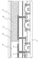
【0025】
反射画素電極と同一の材料でもって周辺回路の配線が形成されているというのは、図6にその具体的な例を示すように、画素電極141を構成する際に、同一材料でもって周辺回路の配線142を形成することをいう。
【0026】
これは、画素電極141を形成する際に、画素電極を構成する図示しない導電膜をパターニングする際に、画素電極141のパターンと配線142のパターンとを同時に形成するとによって実現される。
【0027】
同時に形成されたどうかは、断面の電子顕微鏡写真を撮影し、同一層上に画素電極と配線とは存在するかどうか、またその膜厚は同じかどうか、また不純物測定等によりそれらに材質が同じかかどうかを計測することによって判断することができる。
【0028】
【発明の実施の形態】
図6に示すように反射型の液晶パネルにおいて、画素マトリクスに配置される反射電極141の形成と同時に周辺回路の配線142を形成する。
【0029】
こうすることで、周辺回路を構成する配線を別工程で設けることができ、作製工程と構成を簡略化することができる。
【0030】
さらにまた、反射電極は低抵抗を有する金属材料でもって構成することができるので、同時に形成される周辺駆動の配線も低抵抗なものとして形成することができる。
【0031】
【実施例】
〔実施例1〕
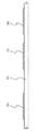
図1乃至図7に本実施例の作製工程の概略を示す。ここでは、反射型のアクティブマトリクス型の液晶表示装置において、画素マトクリクス回路に配置されるNチャネル型のTFTと周辺駆動回路を構成するCMOS回路とを同時に作製する例を示す。
【0032】
まず図1に示すようにガラス基板(または石英基板)101を用意する。基板の平坦性が悪い場合は、その表面に酸化珪素膜や酸化窒化珪素膜を成膜しておくことが好ましい。
【0033】
基板としては、一般に絶縁表面を有する基板を利用することができる。絶縁表面を有する基板としては、ガラス基板、石英基板、ガラス基板や石英基板の表面に酸化珪素膜等の絶縁膜が成膜された基板、シリコンウエハー等の半導体基板の表面に酸化膜を成膜した基板等を挙げることができる。
【0034】
基板101を用意したら、その表面に減圧熱CVD法で図示しない非晶質珪素膜を50nmの厚さに成膜する。
【0035】
次に加熱処理により非晶質珪素膜を結晶化させ、結晶性珪素膜を得る。結晶化の方法としては、レーザー光の照射や強光の照射を利用してもよい。
【0036】
次に得られた結晶性珪素膜をパターニングすることにより、102、103、104で示される島状のパターンを得る。この島状のパターンがTFTの活性層となる。
【0037】
ここで、102が画素マトリクス回路に配置されるNチャネル型TFT(NTFTと記す)の活性層となる。また、103が周辺駆動回路を構成するCMOS回路を構成するPチャネル型TFT(PTFTと記す)の活性層となる。また、104が周辺駆動回路を構成するCMOS回路を構成するNチャネル型TFT(NTFTと記す)の活性層となる。
【0038】
こうして図1に示す状態を得る。次に図2に示すようにゲイト絶縁膜として酸化珪素膜105を100nmの厚さにプラズマCVD法でもって成膜する。
【0039】
さらにアルミニウム膜をスパッタ法でもって400nmの厚さに成膜し、さらにその膜をパターニングすることにより、106、107、108で示すパターンを形成する。このパターンが各TFTのゲイト電極(およびそこから延在したゲイト配線)となる。
【0040】
106、107、108で示すアルミニウムパターンを形成したら、その表面に陽極酸化膜109、110、111を60nmの厚さに成膜する。
【0041】
この陽極酸化膜は、各アルミニウムパターンを電気的に絶縁保護し、また物理的に保護する機能を有している。
【0042】
次にPTFTの上部を図示しないレジストマスクで覆い、P(燐)イオンのドーピングをプラズマドーピング法でもって行う。
【0043】
P(燐)イオンのドーピングを行うことで、画素マトリクスに配置されるNTFTのソース領域112、チャネル領域113、ドレイン領域114が自己整合的に形成される。また、周辺駆動回路のCMOS回路を構成するNTFTのソース領域120、チャネル領域119、ドレイン領域118が自己整合的に形成される。
【0044】
次にPTFTの上部を覆ったレジストマスクを除去し、さらにNTFTの上部にレジストマスクを配置する。この状態でさらにB(ボロン)のドーピングをプラズマドーピング法でもって行う。
【0045】
この工程において、周辺駆動回路のCMOS回路を構成するPTFTのソース領域115、チャネル領域116、ドレイン領域117が自己整合的に形成される。
【0046】
ドーピングが終了したら、図示しないレジストマスクを除去する。そして、レーザー光の照射を行い、不純物がドーピングされた領域の結晶性の改善とドーパント元素の活性化とを行う。
【0047】
こうして図2に示す状態を得る。
【0048】
次に図3に示すように層間絶縁膜として酸化珪素膜121をプラズマCVD法により、500nmの厚さに成膜する。
【0049】
さらにコンタクトホールの形成を行い、図示しないチタン膜とアルミニウム膜とチタン膜との積層膜をスパッタ法でもって成膜する。
【0050】
ここで、このチタン膜の膜厚は各100nm、アルミニウム膜の膜厚は400nmとする。チタン膜は、半導体や電極との電気的なコンタクトを良好なものとするために機能する。
【0051】
次に上記チタン膜とアルミニウム膜とチタン膜との積層膜をパターニングすることにより、図3に示すような状態を得る。
【0052】
図3には、画素マトリクスに配置されるNTFTのソース電極を構成するチタン膜122、アルミニウム膜123、チタン膜124でなるの積層膜パターンが示されている。
【0053】
また、画素マトリクスに配置されるNTFTのドレイン電極を構成するチタン膜125、アルミニウム膜126、チタン膜127でなる積層膜パターンが示されている。
【0054】
また、CMOS回路のPTFTのソース電極を構成するチタン膜128、アルミニウム膜129、チタン膜130でなる積層膜パターンが示されている。
【0055】
また、CMOS回路のPTFTのドレイン電極を構成するチタン膜131、アルミニウム膜132、チタン膜133でなる積層膜パターンが示されている。
【0056】
また、CMOS回路のNTFTのドレイン電極を構成するチタン膜134、アルミニウム膜135、チタン膜136でなる積層膜パターンが示されている。
【0057】
CMOS回路のNTFTのドレイン電極を構成するチタン膜131、アルミニウム膜132、チタン膜133でなる積層膜パターンが示されている。
【0058】
こうして図3に示す状態を得る。
【0059】
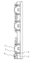
次に図4に示す窒化珪素膜137をプラズマCVD法でもって50nmの厚さに成膜する。この窒化珪素膜137は、補助容量の誘電体膜を構成する。
【0060】
次に図示しないチタン膜をスパッタ法でもって150nmの厚さに成膜する。そしてこの膜をパターニングすることにより、補助容量用の電極パターン138を形成する。
【0061】
補助容量は、チタン膜122、アルミニウム膜123、チタン膜124で構成される電極とチタン電極138との間に誘電体膜として窒化珪素膜137を挟んだものとして構成される。
【0062】
ここで窒化珪素膜は誘電率が大きく、またその厚さを薄くできるので、大きな容量を稼ぐことができる。
【0063】
プロジェクション用の液晶パネルのようにその大きさが2インチ対角以下というような小さなものとなる場合には、画素の面積も小さくなり、一般に補助容量を稼ぐことが困難になる。
【0064】
しかし、本実施例に示すような構造で容量を形成することで上記困難性を解決することができる。
【0065】
図4に示す状態を得たら、図5に示すように層間絶縁膜としてポリイミド樹脂膜139を成膜する。ポリイミド樹脂膜139の膜厚は、最大で1μmとなるよに調整する。
【0066】
ポリイミド以外には、ポリアミド、ポリイミドアミド、エポキシ、アクリル等の樹脂を利用することができる。
【0067】
次に150nm厚のチタン膜をスパッタ法でもって成膜し、それをパターニングすることにより、図5の140で示されるパターンを形成する。このパターンは、その上方に形成される画素電極及び配線と、下方に配置されるTFTや配線と、が互いに電気的に干渉することを防ぐためのシールドパターンとして機能する。
【0068】
また、このシールドパターン140の駆動回路上方の部分は、周辺駆動回路に対して光照射が行われないようにする遮光膜として機能する。
【0069】
こうして図5に示す状態を得る。次にシールドパターン140を覆って絶縁膜を形成した後に、コンタクトホールの形成を行い、画素電極となるアルミニウム膜を350nmの厚さにスパッタ法によって成膜する。
【0070】
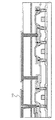
そしてこのアルミニウム膜をパターニングすることにより、画素電極141、周辺駆動回路と画素マトリクスTFTとを接続する配線142とを同時に形成する。(図6)
【0071】
この配線142は、画素電極141を構成するアルミニウム膜を利用して構成されるので、独立した作製工程を採用する必要はない。即ち、この配線142を設けるために工程を増やす必要がない。
【0072】
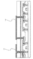
図6に示す状態を得たら、図7に示すように配向膜として機能するポリイミド樹脂でなる配向膜143を150nmの厚さに成膜する。そして配向処理を施しTFTでなる回路が形成された一方の基板が完成する。
【0073】
図7に示す状態を得たら、他方のガラス基板(または石英基板)を用意し、図7に基板(TFT基板と称する)と貼り合わせる。そして、2枚の基板の隙間に液晶を充填し、図8に示す反射型のアクティブマトリクス型液晶パネルを得る。
【0074】
図8に示す液晶パネルにおいて、147が対向基板(TFT側基板に対しての対向基板)であり、146がITOでもって構成された対向電極(TFT基板側に設けられた画素電極141に対向する電極)である。
【0075】
148は封止材(シール材)であって、基板147と基板101とを貼り合わせる機能を有している。また、液晶材料が外部に漏れ出ないように封止する機能を有している。
【0076】
144は液晶材料である。反射型の液晶パネルの場合は、複屈折モードでの表示が行われる。即ち、基板に平行な方向に配向した液晶分子層中を基板面に垂直な方向に進行する光の偏波面が垂直偏波〜楕円偏頗〜円偏波〜楕円偏波〜水平偏波と変化する現象を利用して表示を行う。
【0077】
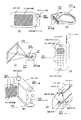
〔実施例2〕
本実施例では、本発明を利用した液晶パネルを備えた装置の例を示す。このような装置としては、ビデオカメラ、デジタルスチルカメラ、ヘッドマウントディスプレイ、カーナビゲーション、パーソナルコンピュータ、携帯情報端末(モバイルコンピュータ、携帯電話等)などが挙げられる。
【0078】
図9(A)に示すのは、モバイルコンピュータであり、本体2001、カメラ部2002、受像部2003、操作スイッチ2004、反射型の液晶パネル2005で構成される。
【0079】
図9(B)はヘッドマウントディスプレイであり、本体2101、反射型の液晶パネル2102、バンド部2103で構成される。
【0080】
図9(C)はフロントプロジェクション型の液晶パネルである。この装置は、光源2202からの光を光学系2204で反射型の液晶表示装置2203に導き、反射型の液晶パネル2203で光学変調された画像を光学系2204で拡大してスクリーン2205に投影するものである。
【0081】
この形式のプロジェクションは、本体2201とは別にスクリーン2205が必要となる。
【0082】
図9(D)は携帯電話であり、本体2301、音声出力部2302、音声入力部2303、反射型の液晶パネル2304、操作スイッチ2305、アンテナ2306で構成される。
【0083】
図9(E)はビデオカメラであり、本体2401、反射型の液晶表示装置2402、音声入力部2403、操作スイッチ2404、バッテリー2405、受像部2406で構成される。
【0084】
図9(F)は、リアプロジェクション型と呼ばれる装置である。この装置は、光源2502から発せられる光を偏光ビームスプリッタ2504で反射型の液晶パネル2503で光学変調し、それをリフレクター2505、2506で反射してスクリンーン2507に投影する。この形式の装置は、本体2501にスクリーン2507が配置されている。
【0085】
〔実施例3〕
本実施例は、実施例1に示す構成において、ゲイト電極としてシリコンを主成分とした材料を用いる場合の例である。
【0086】
図10に本実施例の概略を示す。ここでは、ゲイト電極1001、1002、1003として、一導電型を付与したシリコン材料を用いている。
【0087】
ゲイト電極を構成する他の材料としては、各種シリサイドや金属材料を用いることができる。
【0088】
【発明の効果】
本明細書で開示する発明を利用することで、アクティブマトリクス回路と周辺駆動回路とを一体化構造において、周辺駆動回路に必要とされる多層配線をより簡便に実現することができる。
【図面の簡単な説明】
【図1】 液晶パネルの作製工程を示す断面図。
【図2】 液晶パネルの作製工程を示す断面図。
【図3】 液晶パネルの作製工程を示す断面図。
【図4】 液晶パネルの作製工程を示す断面図。
【図5】 液晶パネルの作製工程を示す断面図。
【図6】 液晶パネルの作製工程を示す断面図。
【図7】 液晶パネルの作製工程を示す断面図。
【図8】 液晶パネルの作製工程を示す断面図。
【図9】 発明を利用した液晶パネルを備えた装置の例を示す図。
【図10】他の実施例を示す図。
【符号の説明】
101 ガラス基板(または石英基板)
102 画素マトリクス回路に配置されるNTFTの活性層
103 周辺駆動回路の配置されるPTFTの活性層
104 周辺駆動回路の配置されるNTFTの活性層
112 ドレイン領域
113 チャネル領域
114 ソース領域
115 ソース領域
116 チャネル領域
117 ドレイン領域
118 ドレイン領域
119 チャネル領域
120 ソース領域
122 チタン膜
123 アルミニウム膜
124 チタン膜
125 チタン膜
126 アルミニウム膜
127 チタン膜
128 チタン膜
129 アルミニウム膜
130 チタン膜
131 チタン膜
132 アルミニウム膜
133 チタン膜
134 チタン膜
135 アルミニウム膜
136 チタン膜
137 窒化珪素膜
138 チタン膜
139 ポリイミド樹脂膜
140 チタン膜
141 画素電極(アルミニウム膜)
142 配線(アルミニウム配線)
143 配向膜(ポリイミド樹脂膜)
144 液晶材料
145 配向膜(ポリイミド樹脂膜)
146 対向電極(ITO電極)
147 対向ガラス基板
148 封止材料[0001]
BACKGROUND OF THE INVENTION
The invention disclosed in this specification relates to a configuration of a reflective liquid crystal display device in which peripheral drive circuits are integrated.
[0002]
[Prior art]
There is known a structure in which an active matrix circuit in which a TFT is arranged in each pixel and a peripheral driving circuit for driving the circuit are integrated on the same substrate. This configuration is referred to as a peripheral drive circuit integrated active matrix display.
[0003]
Until now, the peripheral drive circuit has generally been composed of a circuit represented by a shift register and a bunfer circuit for supplying a signal to the active matrix circuit.
[0004]
However, as a future technology trend, a circuit that can handle image information, various timing signals, etc. (previously configured with an external IC) is also configured with TFTs, and the peripheral drive circuit is on the same substrate as the active matrix circuit. It is thought that the tendency to accumulate will progress.
[0005]
The active matrix circuit basically has a structure in which source lines and gate lines are arranged in a lattice pattern, and TFTs are arranged near the intersections.
[0006]
On the other hand, although the peripheral drive circuit is based on a CMOS circuit, it is expected that the circuit configuration will become increasingly complex in the future.
[0007]
In such a configuration, it is necessary to use multilayer wiring in order to reduce the occupied area.
[0008]
However, forming a new layer to form a multilayer wiring has a problem in that the manufacturing process becomes complicated.
[0009]
[Problems to be solved by the invention]
An object of the invention disclosed in this specification is to provide a configuration that more easily realizes multilayer wiring required for a peripheral drive circuit in an integrated structure of an active matrix circuit and a peripheral drive circuit.
[0010]
[Means for Solving the Problems]
The invention disclosed in this specification focuses on a reflective liquid crystal display device. A reflective liquid crystal display device uses a metal electrode as a reflective electrode. For example, a material mainly composed of aluminum is used.
[0011]
The invention disclosed in this specification focuses on the material of the reflective electrode. That is, with the material constituting the pixel electrode, the wiring arranged in the peripheral drive circuit is formed simultaneously with the formation of the pixel electrode.
[0012]
By doing so, it is possible to form a multilayer wiring required for the peripheral driving circuit without increasing the manufacturing process (the pattern becomes complicated).
[0013]
Since the reflective electrode can be made of a low resistance material such as aluminum, it is suitable for forming the wiring of the peripheral drive circuit.
[0014]
Note that in a transmissive liquid crystal display device, a material having a relatively high resistance, such as ITO, is used for the pixel electrode. Therefore, it is not preferable to use the invention disclosed in this specification.
[0015]
In addition, the peripheral drive circuit in this specification includes a circuit that generates various timing signals, a circuit that handles image information, a circuit that handles image information, and various memory circuits in addition to a circuit that directly drives an active matrix circuit such as a shift register circuit and a buffer circuit. And arithmetic circuits.
[0016]
One of the inventions disclosed in this specification is:
An active matrix circuit;
A peripheral circuit including at least a circuit for driving the active matrix circuit;
Has a structure composed of thin film transistors on the same substrate,
The active matrix circuit is provided with reflective pixel electrodes arranged in a matrix,
The wiring of the peripheral circuit is formed of the same material as the reflective pixel electrode.
[0017]
In the above structure, the active matrix circuit can be exemplified by a structure in which thin film transistors are arranged in the vicinity of intersections of source lines and gate lines arranged in a lattice pattern, and the drains of the thin film transistors are arranged in pixel electrodes.
[0018]
Peripheral circuits include a shift register circuit, an analog switch, a peripheral drive circuit that is usually called a buffer, and a circuit equipped with an oscillation circuit, a circuit that handles image information, a memory circuit, etc. it can.
[0019]
As a future technical trend, it is considered that a peripheral circuit having various functions is required. Therefore, the peripheral circuits in this specification include not only a circuit for driving an active matrix circuit but also a circuit having various functions such as a system on panel.
[0020]
As a type of the thin film transistor, a top gate type, a bottom gate type, or a multi-gate type in which a large number of TFTs are equivalently connected in series can be used.
[0021]
As a material constituting the reflective electrode, it is preferable to use a material having a high reflectivity represented by aluminum and a low resistance.
[0022]
For example, in the case of the VGA standard (640 pixels × 480 pixels), if the screen is rewritten 60 times per second in the circuit on the horizontal scanning side (the peripheral drive circuit side on the source line side), 640 × 480 × 60 = 18.5 MHz Operating speed is required.
[0023]
In the case of the XGA standard (1024 pixels × 768 pixels), an operation speed of 1024 × 768 × 60 = 47 MHz is required.
[0024]
In such a case, it is preferable to employ a wiring having a low resistance as much as possible in the peripheral drive circuit. Therefore, in such a case, the invention disclosed in this specification is extremely useful.
[0025]
The wiring of the peripheral circuit is formed of the same material as that of the reflective pixel electrode. As shown in a specific example in FIG. 6, when the
[0026]
This is realized by simultaneously forming the pattern of the
[0027]
Whether they were formed at the same time was taken by taking an electron micrograph of the cross section, whether the pixel electrode and the wiring existed on the same layer, whether the film thickness was the same, and the same material by impurity measurement etc. It can be determined by measuring whether or not.
[0028]
DETAILED DESCRIPTION OF THE INVENTION
As shown in FIG. 6, in the reflective liquid crystal panel, the
[0029]
Thus, wirings forming the peripheral circuit can be provided in a separate process, and the manufacturing process and the configuration can be simplified.
[0030]
Furthermore, since the reflective electrode can be made of a metal material having a low resistance, the peripheral drive wiring formed simultaneously can also be formed with a low resistance.
[0031]
【Example】
[Example 1]
1 to 7 show an outline of manufacturing steps of this embodiment. Here, an example is shown in which, in a reflective active matrix liquid crystal display device, an N-channel TFT disposed in a pixel matrix circuit and a CMOS circuit constituting a peripheral driver circuit are manufactured at the same time.
[0032]
First, a glass substrate (or quartz substrate) 101 is prepared as shown in FIG. When the flatness of the substrate is poor, it is preferable to form a silicon oxide film or a silicon oxynitride film on the surface.
[0033]
In general, a substrate having an insulating surface can be used as the substrate. As a substrate having an insulating surface, a glass substrate, a quartz substrate, a substrate in which an insulating film such as a silicon oxide film is formed on the surface of a glass substrate or a quartz substrate, or an oxide film is formed on the surface of a semiconductor substrate such as a silicon wafer And the like.
[0034]
When the
[0035]
Next, the amorphous silicon film is crystallized by heat treatment to obtain a crystalline silicon film. As a crystallization method, laser light irradiation or strong light irradiation may be used.
[0036]
Next, by patterning the obtained crystalline silicon film, island-shaped patterns indicated by 102, 103, and 104 are obtained. This island-shaped pattern becomes the active layer of the TFT.
[0037]
Here,
[0038]
Thus, the state shown in FIG. 1 is obtained. Next, as shown in FIG. 2, a
[0039]
Further, an aluminum film is formed by sputtering to a thickness of 400 nm, and the film is further patterned to form
[0040]
After the
[0041]
The anodic oxide film has a function of electrically insulating and protecting each aluminum pattern.
[0042]
Next, the upper part of PTFT is covered with a resist mask (not shown), and P (phosphorus) ions are doped by plasma doping.
[0043]
By doping with P (phosphorus) ions, the
[0044]
Next, the resist mask covering the upper part of the PTFT is removed, and a resist mask is arranged on the upper part of the NTFT. In this state, B (boron) is further doped by plasma doping.
[0045]
In this process, the
[0046]
When the doping is completed, the resist mask (not shown) is removed. Then, laser light irradiation is performed to improve the crystallinity of the region doped with impurities and to activate the dopant element.
[0047]
In this way, the state shown in FIG. 2 is obtained.
[0048]
Next, as shown in FIG. 3, a
[0049]
Further, contact holes are formed, and a laminated film of a titanium film, an aluminum film and a titanium film (not shown) is formed by sputtering.
[0050]
Here, the thickness of the titanium film is 100 nm and the thickness of the aluminum film is 400 nm. The titanium film functions to make good electrical contact with the semiconductor and the electrode.
[0051]
Next, by patterning the laminated film of the titanium film, the aluminum film, and the titanium film, a state as shown in FIG. 3 is obtained.
[0052]
FIG. 3 shows a laminated film pattern composed of a
[0053]
In addition, a laminated film pattern including a
[0054]
Further, a laminated film pattern composed of a
[0055]
Further, a laminated film pattern composed of a
[0056]
In addition, a laminated film pattern including a
[0057]
A laminated film pattern composed of a
[0058]
In this way, the state shown in FIG. 3 is obtained.
[0059]
Next, a
[0060]
Next, a titanium film (not shown) is formed to a thickness of 150 nm by sputtering. Then, the auxiliary
[0061]
The auxiliary capacitance is configured by sandwiching a
[0062]
Here, since the silicon nitride film has a large dielectric constant and can be thinned, a large capacity can be obtained.
[0063]
When the size is as small as 2 inches diagonal or less like a liquid crystal panel for projection, the area of the pixel becomes small, and it is generally difficult to obtain an auxiliary capacity.
[0064]
However, the difficulty can be solved by forming a capacitor with a structure as shown in this embodiment.
[0065]
When the state shown in FIG. 4 is obtained, a
[0066]
In addition to polyimide, resins such as polyamide, polyimide amide, epoxy, and acrylic can be used.
[0067]
Next, a titanium film having a thickness of 150 nm is formed by sputtering, and is patterned to form a pattern indicated by 140 in FIG. This pattern functions as a shield pattern for preventing the pixel electrode and wiring formed above and the TFT and wiring disposed below from electrically interfering with each other.
[0068]
The portion above the drive circuit of the
[0069]
Thus, the state shown in FIG. 5 is obtained. Next , after forming an insulating film covering the
[0070]
Then, by patterning this aluminum film, the
[0071]
Since the
[0072]
When the state shown in FIG. 6 is obtained, an
[0073]
When the state shown in FIG. 7 is obtained, the other glass substrate (or quartz substrate) is prepared and bonded to the substrate (referred to as a TFT substrate) in FIG. Then, a liquid crystal is filled in the gap between the two substrates to obtain a reflective active matrix liquid crystal panel shown in FIG.
[0074]
In the liquid crystal panel shown in FIG. 8,
[0075]
[0076]
144 is a liquid crystal material. In the case of a reflective liquid crystal panel, display in a birefringence mode is performed. That is, the plane of polarization of light traveling in a direction perpendicular to the substrate surface in a liquid crystal molecular layer aligned in a direction parallel to the substrate changes from vertical polarization to elliptical polarization to circular polarization to elliptical polarization to horizontal polarization. Display using the phenomenon.
[0077]
[Example 2]
In this embodiment, an example of an apparatus provided with a liquid crystal panel using the present invention is shown. Examples of such a device include a video camera, a digital still camera, a head mounted display, a car navigation system, a personal computer, a portable information terminal (mobile computer, mobile phone, etc.), and the like.
[0078]
FIG. 9A illustrates a mobile computer, which includes a
[0079]
FIG. 9B illustrates a head mounted display which includes a
[0080]
FIG. 9C illustrates a front projection type liquid crystal panel. In this apparatus, light from a
[0081]
This type of projection requires a
[0082]
FIG. 9D illustrates a mobile phone, which includes a main body 2301, an audio output portion 2302, an audio input portion 2303, a reflective liquid crystal panel 2304, operation switches 2305, and an
[0083]
FIG. 9E illustrates a video camera which includes a
[0084]
FIG. 9F illustrates an apparatus called a rear projection type. In this apparatus, light emitted from a light source 2502 is optically modulated by a reflective liquid crystal panel 2503 by a
[0085]
Example 3
This embodiment is an example in which a material mainly composed of silicon is used as the gate electrode in the configuration shown in the first embodiment.
[0086]
FIG. 10 shows an outline of the present embodiment. Here, as the
[0087]
As other materials constituting the gate electrode, various silicides and metal materials can be used.
[0088]
【The invention's effect】
By utilizing the invention disclosed in this specification, a multilayer wiring required for the peripheral drive circuit can be more easily realized in an integrated structure of the active matrix circuit and the peripheral drive circuit.
[Brief description of the drawings]
FIG. 1 is a cross-sectional view illustrating a manufacturing process of a liquid crystal panel.
FIG. 2 is a cross-sectional view illustrating a manufacturing process of a liquid crystal panel.
FIG. 3 is a cross-sectional view illustrating a manufacturing process of a liquid crystal panel.
FIG. 4 is a cross-sectional view illustrating a manufacturing process of a liquid crystal panel.
FIG. 5 is a cross-sectional view illustrating a manufacturing process of a liquid crystal panel.
6 is a cross-sectional view illustrating a manufacturing process of a liquid crystal panel. FIG.
7 is a cross-sectional view illustrating a manufacturing process of a liquid crystal panel. FIG.
FIG. 8 is a cross-sectional view illustrating a manufacturing process of a liquid crystal panel.
FIG. 9 is a diagram showing an example of an apparatus including a liquid crystal panel using the invention.
FIG. 10 is a diagram showing another embodiment.
[Explanation of symbols]
101 Glass substrate (or quartz substrate)
102 NTFT
142 Wiring (aluminum wiring)
143 Alignment film (polyimide resin film)
144
146 Counter electrode (ITO electrode)
147
Claims (23)
前記周辺駆動回路は、
前記薄膜トランジスタの活性層、ゲイト絶縁膜、およびゲイト電極上に形成された第1の絶縁膜と、
前記第1の絶縁膜上に形成され、前記活性層に接続された第1の電極および第2の電極と、
前記第1の電極および前記第2の電極上に形成された第2の絶縁膜と、
前記第2の絶縁膜上に形成され、前記薄膜トランジスタの上方を覆うシールドパターンと、
前記シールドパターンの上に形成された第3の絶縁膜と、
を有し、
前記第3の絶縁膜上に形成され、前記第1の電極に接続された前記周辺駆動回路と画素マトリクス回路とを接続する配線を有し、
前記画素電極および前記配線は、同一材料からなり、
前記画素電極が第3の絶縁膜上で且つ前記配線と同じ層に形成されていることを特徴とする表示装置。A display device using a peripheral drive circuit having a thin film transistor and a pixel matrix circuit having a pixel electrode,
The peripheral drive circuit is
An active layer of the thin film transistor, a gate insulating film, and a first insulating film formed on the gate electrode;
A first electrode and a second electrode formed on the first insulating film and connected to the active layer;
A second insulating film formed on the first electrode and the second electrode;
A shield pattern formed on the second insulating film and covering the thin film transistor;
A third insulating film formed on the shield pattern;
Have
A wiring formed on the third insulating film and connecting the peripheral drive circuit connected to the first electrode and a pixel matrix circuit;
The pixel electrode and the wiring, Ri Do the same material,
Display device comprising Rukoto said pixel electrodes are formed on the third and the same layer as the wiring on the insulating film.
前記周辺駆動回路は、
前記薄膜トランジスタの活性層、ゲイト絶縁膜、よびゲイト電極上に形成された第1の絶縁膜と、
前記第1の絶縁膜上に形成され、前記活性層に接続された第1の電極および第2の電極と、
前記第1の電極および前記第2の電極上に形成された窒化珪素膜と、
前記窒化珪素膜上に形成された第2の絶縁膜と、
前記第2の絶縁膜上に形成され、前記薄膜トランジスタの上方を覆うシールドパターンと、
前記シールドパターンの上に形成された第3の絶縁膜と、
を有し、
前記第3の絶縁膜上に形成され、前記第1の電極に接続された前記周辺駆動回路と画素マトリクス回路とを接続する配線を有し、
前記画素電極および前記配線は、同一材料からなり、
前記画素電極が第3の絶縁膜上で且つ前記配線と同じ層に形成されていることを特徴とする表示装置。A display device using a peripheral drive circuit having a thin film transistor and a pixel matrix circuit having a pixel electrode,
The peripheral drive circuit is
An active layer of the thin film transistor, a gate insulating film, and a first insulating film formed on the gate electrode;
A first electrode and a second electrode formed on the first insulating film and connected to the active layer;
A silicon nitride film formed on the first electrode and the second electrode;
A second insulating film formed on the silicon nitride film;
A shield pattern formed on the second insulating film and covering the thin film transistor;
A third insulating film formed on the shield pattern;
Have
A wiring formed on the third insulating film and connecting the peripheral drive circuit connected to the first electrode and a pixel matrix circuit;
The pixel electrode and the wiring, Ri Do the same material,
Display device comprising Rukoto said pixel electrodes are formed on the third and the same layer as the wiring on the insulating film.
前記周辺駆動回路は、
前記薄膜トランジスタの活性層、ゲイト絶縁膜、およびゲイト電極上に形成された第1の絶縁膜と、
前記第1の絶縁膜上に形成され、前記活性層に接続された第1の電極および第2の電極と、
前記第1の電極および前記第2の電極上に形成された窒化珪素膜と、
前記窒化珪素膜上に形成された第2の絶縁膜と、
前記第2の絶縁膜上に形成され、前記薄膜トランジスタの上方を覆うシールドパターンと、
前記シールドパターンの上に形成された第3の絶縁膜と、
を有し、
前記第3の絶縁膜上に形成され、前記第1の電極に接続された前記周辺駆動回路と画素マトリクス回路とを接続する配線と、
前記配線の上方に形成されたシール材とを有し、
前記画素電極および前記配線は、同一材料からなり、
前記画素電極が第3の絶縁膜上で且つ前記配線と同じ層に形成されていることを特徴とする表示装置。A display device using a peripheral drive circuit having a thin film transistor and a pixel matrix circuit having a pixel electrode,
The peripheral drive circuit is
An active layer of the thin film transistor, a gate insulating film, and a first insulating film formed on the gate electrode;
A first electrode and a second electrode formed on the first insulating film and connected to the active layer;
A silicon nitride film formed on the first electrode and the second electrode;
A second insulating film formed on the silicon nitride film;
A shield pattern formed on the second insulating film and covering the thin film transistor;
A third insulating film formed on the shield pattern;
Have
A wiring formed on the third insulating film and connected to the peripheral electrode circuit connected to the first electrode and a pixel matrix circuit;
A sealing material formed above the wiring,
The pixel electrode and the wiring, Ri Do the same material,
Display device comprising Rukoto said pixel electrodes are formed on the third and the same layer as the wiring on the insulating film.
前記周辺駆動回路はCMOS回路を有することを特徴とする表示装置。In any one of Claims 1 thru | or 3,
The display device, wherein the peripheral driver circuit includes a CMOS circuit.
前記画素電極及び前記配線は、アルミニウムからなることを特徴とする表示装置。In any one of Claims 1 thru | or 4,
The display device, wherein the pixel electrode and the wiring are made of aluminum.
前記第2の絶縁膜は、樹脂膜であることを特徴とする表示装置。In any one of Claims 1 thru | or 5,
The display device, wherein the second insulating film is a resin film.
前記樹脂膜は、ポリイミド、ポリアミド、ポリイミドアミド、エポキシまたはアクリルのいずれか一からなる樹脂膜であることを特徴とする表示装置。In claim 6,
The display device, wherein the resin film is a resin film made of any one of polyimide, polyamide, polyimide amide, epoxy, and acrylic.
前記ゲイト電極は、シリコンを主成分とした材料、シリサイドまたは金属材料からなることを特徴とする表示装置。In any one of Claims 1 thru | or 7,
The display device according to claim 1, wherein the gate electrode is made of silicon, a silicide, or a metal material.
前記シールドパターンはチタン膜からなることを特徴とする表示装置。In any one of Claims 1 thru | or 8,
The display device, wherein the shield pattern is made of a titanium film.
前記第1の電極および前記第2の電極は、アルミニウム膜と前記アルミニウム膜の上下
に接して形成されたチタン膜との積層構造からなることを特徴とする表示装置。In any one of Claims 1 thru | or 9,
The display device, wherein the first electrode and the second electrode have a laminated structure of an aluminum film and a titanium film formed in contact with the aluminum film above and below the aluminum film.
前記薄膜トランジスタは、トップゲイト型、ボトムゲイト型またはマルチゲイト型の薄膜トランジスタであることを特徴とする表示装置。In any one of Claims 1 to 10,
The display device, wherein the thin film transistor is a top gate type, bottom gate type, or multigate type thin film transistor.
前記第1の絶縁膜は、酸化珪素膜であることを特徴とする表示装置。In any one of Claims 1 to 11,
The display device, wherein the first insulating film is a silicon oxide film.
前記画素マトリクス回路と前記周辺駆動回路は同一基板上に形成されていることを特徴とする表示装置。In any one of Claims 1 to 12,
The display device, wherein the pixel matrix circuit and the peripheral driving circuit are formed on the same substrate.
前記画素マトリクス回路はNチャネル型薄膜トランジスタを有することを特徴とする表示装置。In any one of Claims 1 thru / or Claim 13,
The display device, wherein the pixel matrix circuit includes an N-channel thin film transistor.
前記周辺駆動回路は、シフトレジスタ回路、バッファー回路、発振回路、画像情報を扱う回路またはメモリー回路のいずれか一を含むことを特徴とする表示装置。In any one of Claims 1 thru | or 14,
The display device, wherein the peripheral driving circuit includes any one of a shift register circuit, a buffer circuit, an oscillation circuit, a circuit for handling image information, or a memory circuit.
前記画素マトリクス回路の上方に液晶材料が配置され、前記周辺駆動回路の上方にシール材が配置された液晶表示装置であることを特徴とする表示装置。The display device according to any one of claims 1, 2, and 4 to 15,
A display device, wherein a liquid crystal material is disposed above the pixel matrix circuit, and a sealing material is disposed above the peripheral drive circuit.
Priority Applications (8)
| Application Number | Priority Date | Filing Date | Title |
|---|---|---|---|
| JP11354997A JP3856901B2 (en) | 1997-04-15 | 1997-04-15 | Display device |
| US09/058,870 US6400426B1 (en) | 1997-04-15 | 1998-04-13 | Reflective liquid crystal display panel and device using same |
| KR1019980013390A KR100553112B1 (en) | 1997-04-15 | 1998-04-15 | Reflective liquid crystal display panels and devices using them |
| US10/127,581 US6967696B2 (en) | 1997-04-15 | 2002-04-23 | Reflective liquid crystal display panel and device using same |
| US11/282,483 US7675583B2 (en) | 1997-04-15 | 2005-11-21 | Reflective liquid crystal display panel and device using same |
| US12/683,473 US8031284B2 (en) | 1997-04-15 | 2010-01-07 | Reflective liquid crystal display panel and device using same |
| US13/247,342 US8405789B2 (en) | 1997-04-15 | 2011-09-28 | Reflective liquid crystal display panel and device using same |
| US13/848,234 US8576348B2 (en) | 1997-04-15 | 2013-03-21 | Reflective liquid crystal display panel and device using same |
Applications Claiming Priority (1)
| Application Number | Priority Date | Filing Date | Title |
|---|---|---|---|
| JP11354997A JP3856901B2 (en) | 1997-04-15 | 1997-04-15 | Display device |
Related Child Applications (1)
| Application Number | Title | Priority Date | Filing Date |
|---|---|---|---|
| JP2006067421A Division JP3857302B2 (en) | 2006-03-13 | 2006-03-13 | Display device |
Publications (2)
| Publication Number | Publication Date |
|---|---|
| JPH10288797A JPH10288797A (en) | 1998-10-27 |
| JP3856901B2 true JP3856901B2 (en) | 2006-12-13 |
Family
ID=14615131
Family Applications (1)
| Application Number | Title | Priority Date | Filing Date |
|---|---|---|---|
| JP11354997A Expired - Fee Related JP3856901B2 (en) | 1997-04-15 | 1997-04-15 | Display device |
Country Status (3)
| Country | Link |
|---|---|
| US (6) | US6400426B1 (en) |
| JP (1) | JP3856901B2 (en) |
| KR (1) | KR100553112B1 (en) |
Cited By (1)
| Publication number | Priority date | Publication date | Assignee | Title |
|---|---|---|---|---|
| KR101337319B1 (en) | 2006-10-04 | 2013-12-06 | 가부시키가이샤 한도오따이 에네루기 켄큐쇼 | Semiconductor device and manufacturing method thereof |
Families Citing this family (27)
| Publication number | Priority date | Publication date | Assignee | Title |
|---|---|---|---|---|
| GB9825314D0 (en) * | 1998-11-20 | 1999-01-13 | Koninkl Philips Electronics Nv | Active matrix liquid crystal display devices |
| US6541294B1 (en) | 1999-07-22 | 2003-04-01 | Semiconductor Energy Laboratory Co., Ltd. | Semiconductor device and manufacturing method thereof |
| JP2002040486A (en) | 2000-05-19 | 2002-02-06 | Seiko Epson Corp | Electrooptic device and its manufacturing method, and electronic equipment |
| JP4827984B2 (en) * | 2000-05-29 | 2011-11-30 | 株式会社半導体エネルギー研究所 | Method for manufacturing liquid crystal display device |
| US7019718B2 (en) * | 2000-07-25 | 2006-03-28 | Semiconductor Energy Laboratory Co., Ltd. | Display device |
| US6734924B2 (en) | 2000-09-08 | 2004-05-11 | Semiconductor Energy Laboratory Co., Ltd. | Liquid crystal display device |
| JP2002162646A (en) * | 2000-09-14 | 2002-06-07 | Sony Corp | Reflection type liquid crystal display device |
| JP2002229061A (en) * | 2001-02-01 | 2002-08-14 | Sony Corp | Thin-film semiconductor device and reflection-type display device |
| JP2002244585A (en) * | 2001-02-02 | 2002-08-30 | Koninkl Philips Electronics Nv | Picture display device |
| US6731572B2 (en) * | 2001-04-12 | 2004-05-04 | Samsung Electronics Co., Ltd. | Optical pickup actuator, optical pickup employing the optical pickup actuator, and optical recording and/or reproducing apparatus employing the optical pickup |
| US6686977B2 (en) * | 2001-07-24 | 2004-02-03 | Three-Five Systems, Inc. | Liquid crystal on silicon device |
| JP2003076298A (en) * | 2001-09-05 | 2003-03-14 | Toshiba Corp | Display device |
| JP4634673B2 (en) * | 2001-09-26 | 2011-02-16 | シャープ株式会社 | Liquid crystal display device and manufacturing method thereof |
| JP3983037B2 (en) * | 2001-11-22 | 2007-09-26 | 株式会社半導体エネルギー研究所 | Light emitting device and manufacturing method thereof |
| JP2003316284A (en) * | 2002-04-24 | 2003-11-07 | Sanyo Electric Co Ltd | Display device |
| JP4073239B2 (en) * | 2002-04-24 | 2008-04-09 | 三洋電機株式会社 | Display device |
| JP4019868B2 (en) * | 2002-09-11 | 2007-12-12 | セイコーエプソン株式会社 | Electro-optical device and electronic apparatus |
| JP4085369B2 (en) * | 2002-10-10 | 2008-05-14 | 日本ビクター株式会社 | Liquid crystal display |
| AU2003284470A1 (en) * | 2002-12-10 | 2004-06-30 | Semiconductor Energy Laboratory Co., Ltd. | Light-emitting device and its fabricating method |
| US7486341B2 (en) * | 2005-11-03 | 2009-02-03 | University Of Central Florida Research Foundation, Inc. | Head mounted display with eye accommodation having 3-D image producing system consisting of, for each eye, one single planar display screen, one single planar tunable focus LC micro-lens array, one single planar black mask and bias lens |
| KR101250790B1 (en) * | 2006-06-30 | 2013-04-04 | 엘지디스플레이 주식회사 | Method of fabricating liquid crystal display device |
| US8354674B2 (en) * | 2007-06-29 | 2013-01-15 | Semiconductor Energy Laboratory Co., Ltd. | Semiconductor device wherein a property of a first semiconductor layer is different from a property of a second semiconductor layer |
| KR101540341B1 (en) * | 2008-10-17 | 2015-07-30 | 삼성전자주식회사 | Panel structure, display device comprising the panel structure and manufacturing methods thereof |
| JP5515281B2 (en) * | 2008-12-03 | 2014-06-11 | ソニー株式会社 | THIN FILM TRANSISTOR, DISPLAY DEVICE, ELECTRONIC DEVICE, AND METHOD FOR PRODUCING THIN FILM TRANSISTOR |
| JP4752927B2 (en) * | 2009-02-09 | 2011-08-17 | ソニー株式会社 | Thin film transistor and display device |
| JP5236812B2 (en) * | 2009-09-11 | 2013-07-17 | シャープ株式会社 | Active matrix substrate and active matrix display device |
| JP2012208294A (en) * | 2011-03-29 | 2012-10-25 | Seiko Epson Corp | Method for manufacturing electro-optic device, electro-optic device, projection-type display device, and electronic equipment |
Family Cites Families (53)
| Publication number | Priority date | Publication date | Assignee | Title |
|---|---|---|---|---|
| US4103297A (en) | 1976-12-20 | 1978-07-25 | Hughes Aircraft Company | Light-insensitive matrix addressed liquid crystal display system |
| US5032883A (en) | 1987-09-09 | 1991-07-16 | Casio Computer Co., Ltd. | Thin film transistor and method of manufacturing the same |
| US5327001A (en) | 1987-09-09 | 1994-07-05 | Casio Computer Co., Ltd. | Thin film transistor array having single light shield layer over transistors and gate and drain lines |
| JP2653099B2 (en) * | 1988-05-17 | 1997-09-10 | セイコーエプソン株式会社 | Active matrix panel, projection display and viewfinder |
| CA1313563C (en) | 1988-10-26 | 1993-02-09 | Makoto Sasaki | Thin film transistor panel |
| US5264077A (en) | 1989-06-15 | 1993-11-23 | Semiconductor Energy Laboratory Co., Ltd. | Method for producing a conductive oxide pattern |
| US5498573A (en) * | 1989-11-29 | 1996-03-12 | General Electric Company | Method of making multi-layer address lines for amorphous silicon liquid crystal display devices |
| US5200847A (en) * | 1990-05-01 | 1993-04-06 | Casio Computer Co., Ltd. | Liquid crystal display device having driving circuit forming on a heat-resistant sub-substrate |
| US5056895A (en) | 1990-05-21 | 1991-10-15 | Greyhawk Systems, Inc. | Active matrix liquid crystal liquid crystal light valve including a dielectric mirror upon a leveling layer and having fringing fields |
| JPH0465168A (en) * | 1990-07-05 | 1992-03-02 | Hitachi Ltd | Thin film transistor |
| US5182624A (en) | 1990-08-08 | 1993-01-26 | Minnesota Mining And Manufacturing Company | Solid state electromagnetic radiation detector fet array |
| US5849601A (en) * | 1990-12-25 | 1998-12-15 | Semiconductor Energy Laboratory Co., Ltd. | Electro-optical device and method for manufacturing the same |
| KR950013784B1 (en) | 1990-11-20 | 1995-11-16 | 가부시키가이샤 한도오따이 에네루기 겐큐쇼 | Field effect trasistor and its making method and tft |
| KR950001360B1 (en) | 1990-11-26 | 1995-02-17 | 가부시키가이샤 한도오따이 에네루기 겐큐쇼 | Electric optical device and driving method thereof |
| JP2999271B2 (en) * | 1990-12-10 | 2000-01-17 | 株式会社半導体エネルギー研究所 | Display device |
| EP0499979A3 (en) | 1991-02-16 | 1993-06-09 | Semiconductor Energy Laboratory Co., Ltd. | Electro-optical device |
| JP2794678B2 (en) | 1991-08-26 | 1998-09-10 | 株式会社 半導体エネルギー研究所 | Insulated gate semiconductor device and method of manufacturing the same |
| US5946561A (en) | 1991-03-18 | 1999-08-31 | Semiconductor Energy Laboratory Co., Ltd. | Semiconductor device and method for forming the same |
| JP3071851B2 (en) | 1991-03-25 | 2000-07-31 | 株式会社半導体エネルギー研究所 | Electro-optical device |
| JP2794499B2 (en) | 1991-03-26 | 1998-09-03 | 株式会社半導体エネルギー研究所 | Method for manufacturing semiconductor device |
| US5414442A (en) | 1991-06-14 | 1995-05-09 | Semiconductor Energy Laboratory Co., Ltd. | Electro-optical device and method of driving the same |
| JPH055898A (en) * | 1991-06-27 | 1993-01-14 | Casio Comput Co Ltd | Thin-film element forming panel |
| US5305519A (en) | 1991-10-24 | 1994-04-26 | Kawasaki Steel Corporation | Multilevel interconnect structure and method of manufacturing the same |
| JP3064596B2 (en) | 1991-11-29 | 2000-07-12 | セイコーエプソン株式会社 | Liquid crystal panel and method of manufacturing the same |
| US5485019A (en) * | 1992-02-05 | 1996-01-16 | Semiconductor Energy Laboratory Co., Ltd. | Semiconductor device and method for forming the same |
| KR940002642A (en) * | 1992-07-02 | 1994-02-17 | 이헌조 | Reflective Active Matrix Liquid Crystal Display |
| FR2693249B1 (en) * | 1992-07-03 | 1994-09-16 | Hutchinson | Method of connecting tubes or pipes, fittings and similar devices obtained by its implementation. |
| KR970010652B1 (en) | 1992-07-06 | 1997-06-30 | 가부시키가이샤 한도오따이 에네루기 겐큐쇼 | Semiconductor device and method of for forming the same |
| JP3345089B2 (en) | 1993-03-26 | 2002-11-18 | 株式会社半導体エネルギー研究所 | Method for manufacturing color filter substrate |
| JP2789293B2 (en) | 1993-07-14 | 1998-08-20 | 株式会社半導体エネルギー研究所 | Semiconductor device manufacturing method |
| JP3109967B2 (en) | 1993-12-28 | 2000-11-20 | キヤノン株式会社 | Active matrix substrate manufacturing method |
| JPH07302912A (en) | 1994-04-29 | 1995-11-14 | Semiconductor Energy Lab Co Ltd | Semiconductor device |
| JP3126630B2 (en) * | 1994-06-20 | 2001-01-22 | キヤノン株式会社 | display |
| US6011607A (en) * | 1995-02-15 | 2000-01-04 | Semiconductor Energy Laboratory Co., | Active matrix display with sealing material |
| TW344901B (en) | 1995-02-15 | 1998-11-11 | Handotai Energy Kenkyusho Kk | Active matrix display device |
| JP3364081B2 (en) | 1995-02-16 | 2003-01-08 | 株式会社半導体エネルギー研究所 | Method for manufacturing semiconductor device |
| US6081305A (en) | 1995-05-30 | 2000-06-27 | Hitachi, Ltd. | Liquid crystal light valve and projection type liquid crystal display using such valve |
| JP3176021B2 (en) * | 1995-05-30 | 2001-06-11 | 株式会社日立製作所 | Liquid crystal light valve and projection type liquid crystal display using the same |
| JP3307181B2 (en) * | 1995-07-31 | 2002-07-24 | ソニー株式会社 | Transmissive display |
| JP3295679B2 (en) | 1995-08-04 | 2002-06-24 | 株式会社半導体エネルギー研究所 | Method for manufacturing semiconductor device |
| KR100338480B1 (en) | 1995-08-19 | 2003-01-24 | 엘지.필립스 엘시디 주식회사 | Liquid crystal display and method for fabricating the same |
| JPH0968726A (en) * | 1995-09-01 | 1997-03-11 | Pioneer Video Corp | Reflection type liquid crystal display device |
| JP3228399B2 (en) | 1995-09-12 | 2001-11-12 | シャープ株式会社 | Liquid crystal display |
| TW371776B (en) | 1995-10-15 | 1999-10-11 | Semiconductor Energy Lab Co Ltd | Laser irradiation apparatus and method |
| US6027960A (en) | 1995-10-25 | 2000-02-22 | Semiconductor Energy Laboratory Co., Ltd. | Laser annealing method and laser annealing device |
| US6015724A (en) | 1995-11-02 | 2000-01-18 | Semiconductor Energy Laboratory Co. | Manufacturing method of a semiconductor device |
| TW329500B (en) | 1995-11-14 | 1998-04-11 | Handotai Energy Kenkyusho Kk | Electro-optical device |
| TWI228625B (en) | 1995-11-17 | 2005-03-01 | Semiconductor Energy Lab | Display device |
| US5847410A (en) | 1995-11-24 | 1998-12-08 | Semiconductor Energy Laboratory Co. | Semiconductor electro-optical device |
| TW309633B (en) | 1995-12-14 | 1997-07-01 | Handotai Energy Kenkyusho Kk | |
| JPH09172070A (en) | 1995-12-18 | 1997-06-30 | Matsushita Electric Ind Co Ltd | Manufacture of semiconductor device |
| US6005648A (en) | 1996-06-25 | 1999-12-21 | Semiconductor Energy Laboratory Co., Ltd. | Display device |
| US5866484A (en) | 1996-07-09 | 1999-02-02 | Nippon Steel Corporation | Semiconductor device and process of producing same |
-
1997
- 1997-04-15 JP JP11354997A patent/JP3856901B2/en not_active Expired - Fee Related
-
1998
- 1998-04-13 US US09/058,870 patent/US6400426B1/en not_active Expired - Lifetime
- 1998-04-15 KR KR1019980013390A patent/KR100553112B1/en not_active IP Right Cessation
-
2002
- 2002-04-23 US US10/127,581 patent/US6967696B2/en not_active Expired - Fee Related
-
2005
- 2005-11-21 US US11/282,483 patent/US7675583B2/en not_active Expired - Fee Related
-
2010
- 2010-01-07 US US12/683,473 patent/US8031284B2/en not_active Expired - Fee Related
-
2011
- 2011-09-28 US US13/247,342 patent/US8405789B2/en not_active Expired - Fee Related
-
2013
- 2013-03-21 US US13/848,234 patent/US8576348B2/en not_active Expired - Fee Related
Cited By (2)
| Publication number | Priority date | Publication date | Assignee | Title |
|---|---|---|---|---|
| KR101337319B1 (en) | 2006-10-04 | 2013-12-06 | 가부시키가이샤 한도오따이 에네루기 켄큐쇼 | Semiconductor device and manufacturing method thereof |
| KR101406770B1 (en) | 2006-10-04 | 2014-06-12 | 가부시키가이샤 한도오따이 에네루기 켄큐쇼 | Semiconductor device and manufacturing method thereof |
Also Published As
| Publication number | Publication date |
|---|---|
| US20020123175A1 (en) | 2002-09-05 |
| JPH10288797A (en) | 1998-10-27 |
| US6967696B2 (en) | 2005-11-22 |
| US20060072059A1 (en) | 2006-04-06 |
| US20130215351A1 (en) | 2013-08-22 |
| US8031284B2 (en) | 2011-10-04 |
| US6400426B1 (en) | 2002-06-04 |
| US20120019739A1 (en) | 2012-01-26 |
| US8405789B2 (en) | 2013-03-26 |
| US8576348B2 (en) | 2013-11-05 |
| KR100553112B1 (en) | 2006-07-06 |
| US7675583B2 (en) | 2010-03-09 |
| KR19980081413A (en) | 1998-11-25 |
| US20100134709A1 (en) | 2010-06-03 |
Similar Documents
| Publication | Publication Date | Title |
|---|---|---|
| JP3856901B2 (en) | Display device | |
| KR100663879B1 (en) | A semiconductor device and method of manufacturing thereof | |
| US7397518B1 (en) | Active matrix liquid crystal with capacitor below disclination region | |
| US7599038B2 (en) | Display apparatus and manufacturing method of display apparatus | |
| JP3607016B2 (en) | Semiconductor device and manufacturing method thereof, and portable information processing terminal, head mounted display, navigation system, mobile phone, camera, and projector | |
| JP2001250953A (en) | Semiconductor device and method of manufacturing the same | |
| JP2006250985A (en) | Electrooptical apparatus and electronic device | |
| JP2004006651A (en) | Method of manufacturing electrooptic device, electrooptic device, method of manufacturing semiconductor device, semiconductor device, projection type display device, and electronic equipment | |
| JP2002082630A (en) | Electro-optic device | |
| JP3857302B2 (en) | Display device | |
| JP2001085693A (en) | Method for manufacturing semiocnductor device, electro- optical device and electronic apparatus | |
| JP2004006652A (en) | Method of manufacturing electrooptic device, electrooptic device, method of manufacturing semiconductor device, semiconductor device, projection type display device, and electronic equipment |
Legal Events
| Date | Code | Title | Description |
|---|---|---|---|
| A521 | Request for written amendment filed |
Free format text: JAPANESE INTERMEDIATE CODE: A523 Effective date: 20040408 |
|
| A621 | Written request for application examination |
Free format text: JAPANESE INTERMEDIATE CODE: A621 Effective date: 20040408 |
|
| A977 | Report on retrieval |
Free format text: JAPANESE INTERMEDIATE CODE: A971007 Effective date: 20051228 |
|
| A131 | Notification of reasons for refusal |
Free format text: JAPANESE INTERMEDIATE CODE: A131 Effective date: 20060117 |
|
| A521 | Request for written amendment filed |
Free format text: JAPANESE INTERMEDIATE CODE: A523 Effective date: 20060317 |
|
| RD02 | Notification of acceptance of power of attorney |
Free format text: JAPANESE INTERMEDIATE CODE: A7422 Effective date: 20060317 |
|
| A131 | Notification of reasons for refusal |
Free format text: JAPANESE INTERMEDIATE CODE: A131 Effective date: 20060509 |
|
| A521 | Request for written amendment filed |
Free format text: JAPANESE INTERMEDIATE CODE: A523 Effective date: 20060707 |
|
| TRDD | Decision of grant or rejection written | ||
| A01 | Written decision to grant a patent or to grant a registration (utility model) |
Free format text: JAPANESE INTERMEDIATE CODE: A01 Effective date: 20060912 |
|
| A61 | First payment of annual fees (during grant procedure) |
Free format text: JAPANESE INTERMEDIATE CODE: A61 Effective date: 20060913 |
|
| R150 | Certificate of patent or registration of utility model |
Free format text: JAPANESE INTERMEDIATE CODE: R150 |
|
| FPAY | Renewal fee payment (event date is renewal date of database) |
Free format text: PAYMENT UNTIL: 20090922 Year of fee payment: 3 |
|
| FPAY | Renewal fee payment (event date is renewal date of database) |
Free format text: PAYMENT UNTIL: 20090922 Year of fee payment: 3 |
|
| FPAY | Renewal fee payment (event date is renewal date of database) |
Free format text: PAYMENT UNTIL: 20100922 Year of fee payment: 4 |
|
| FPAY | Renewal fee payment (event date is renewal date of database) |
Free format text: PAYMENT UNTIL: 20100922 Year of fee payment: 4 |
|
| FPAY | Renewal fee payment (event date is renewal date of database) |
Free format text: PAYMENT UNTIL: 20110922 Year of fee payment: 5 |
|
| FPAY | Renewal fee payment (event date is renewal date of database) |
Free format text: PAYMENT UNTIL: 20110922 Year of fee payment: 5 |
|
| FPAY | Renewal fee payment (event date is renewal date of database) |
Free format text: PAYMENT UNTIL: 20120922 Year of fee payment: 6 |
|
| FPAY | Renewal fee payment (event date is renewal date of database) |
Free format text: PAYMENT UNTIL: 20120922 Year of fee payment: 6 |
|
| FPAY | Renewal fee payment (event date is renewal date of database) |
Free format text: PAYMENT UNTIL: 20130922 Year of fee payment: 7 |
|
| R250 | Receipt of annual fees |
Free format text: JAPANESE INTERMEDIATE CODE: R250 |
|
| R250 | Receipt of annual fees |
Free format text: JAPANESE INTERMEDIATE CODE: R250 |
|
| R250 | Receipt of annual fees |
Free format text: JAPANESE INTERMEDIATE CODE: R250 |
|
| LAPS | Cancellation because of no payment of annual fees |