JP3856473B2 - Incoherent radiation source lighting method and illumination device suitable therefor - Google Patents
Incoherent radiation source lighting method and illumination device suitable therefor Download PDFInfo
- Publication number
- JP3856473B2 JP3856473B2 JP50616597A JP50616597A JP3856473B2 JP 3856473 B2 JP3856473 B2 JP 3856473B2 JP 50616597 A JP50616597 A JP 50616597A JP 50616597 A JP50616597 A JP 50616597A JP 3856473 B2 JP3856473 B2 JP 3856473B2
- Authority
- JP
- Japan
- Prior art keywords
- discharge
- discharge tube
- electrodes
- radiation source
- wall
- Prior art date
- Legal status (The legal status is an assumption and is not a legal conclusion. Google has not performed a legal analysis and makes no representation as to the accuracy of the status listed.)
- Expired - Fee Related
Links
Images


Classifications
-
- H—ELECTRICITY
- H01—ELECTRIC ELEMENTS
- H01J—ELECTRIC DISCHARGE TUBES OR DISCHARGE LAMPS
- H01J65/00—Lamps without any electrode inside the vessel; Lamps with at least one main electrode outside the vessel
- H01J65/04—Lamps in which a gas filling is excited to luminesce by an external electromagnetic field or by external corpuscular radiation, e.g. for indicating plasma display panels
- H01J65/042—Lamps in which a gas filling is excited to luminesce by an external electromagnetic field or by external corpuscular radiation, e.g. for indicating plasma display panels by an external electromagnetic field
- H01J65/046—Lamps in which a gas filling is excited to luminesce by an external electromagnetic field or by external corpuscular radiation, e.g. for indicating plasma display panels by an external electromagnetic field the field being produced by using capacitive means around the vessel
-
- H—ELECTRICITY
- H01—ELECTRIC ELEMENTS
- H01J—ELECTRIC DISCHARGE TUBES OR DISCHARGE LAMPS
- H01J61/00—Gas-discharge or vapour-discharge lamps
- H01J61/02—Details
- H01J61/30—Vessels; Containers
- H01J61/305—Flat vessels or containers
-
- H—ELECTRICITY
- H05—ELECTRIC TECHNIQUES NOT OTHERWISE PROVIDED FOR
- H05B—ELECTRIC HEATING; ELECTRIC LIGHT SOURCES NOT OTHERWISE PROVIDED FOR; CIRCUIT ARRANGEMENTS FOR ELECTRIC LIGHT SOURCES, IN GENERAL
- H05B41/00—Circuit arrangements or apparatus for igniting or operating discharge lamps
- H05B41/14—Circuit arrangements
- H05B41/24—Circuit arrangements in which the lamp is fed by high frequency ac, or with separate oscillator frequency
Description
技術分野
本発明は少なくとも一部分が透明であり、封入ガスを封入されて閉鎖された又はガス又は混合ガスが通流する開放された非導電材料製放電管と、互いにかつ放電管の内部から誘電体材料によって分離された電極とを備えたインコヒーレント放射源、特に放電ランプを誘電体妨害放電によって点灯する方法に関する。
さらに、本発明は、放射源と、放射源に電圧を印加する電源とを備えた照明装置であって、放射源は、少なくとも一部分が透明であり、封入ガスを封入されて閉鎖された又はガスもしくは混合ガスが通流する開放された非導電材料製放電管と、互いにかつ放電管の内部から誘電体材料によって分離され電源に接続された電極とから構成され、放射源からの放射はインコヒーレントに放出され、放射源は誘電体妨害放電に適する照明装置に関する。
インコヒーレント放射源とは紫外線放射器及び赤外線放射器ならびに特に可視光を放射する放電ランプと理解されるべきものである。
産業上の適応性
この種の放射源は、放出した放射のスペクトルに応じて、全般照明及び補助照明(例えば住宅照明及び事務所照明もしくは表示装置(例えば液晶ディスプレイ)のバックグランド照明)、交通・信号照明、紫外線照射(例えば殺菌又は光分解)ならびに赤外線照射(例えばレジストの乾燥)に適している。
従来技術
国際公開第94/23442号パンフレットには、誘電体妨害放電によってインコヒーレント放射源、特に放電ランプを点灯する方法が記載されている。この点灯方法は電圧パルス列を用い、その場合個々の電圧パルスは休止時間によって互いに分離されている。このパルス点灯方法の利点は放射発生の高い効率にある。
欧州特許出願公開第0363832号明細書には、高電圧源の両極に一対で接続された電極を備える紫外線高出力放射器が記載されている。この放射器では電極は互いにかつ放射器の放電室から誘電体材料によって分離されている。この種の電極は以下においては短縮して“誘電体電極”と称される。さらに、電極は並置され、これによって比較的平らな放電管を用いた平坦状放電を実現することができる。誘電体電極には数kHz以下の交流電流の範囲の周波数で数百V〜20000Vのオーダの交流電圧が印加され、それにより沿面放電が主として誘電体表面の領域のみに形成される。
重要な欠点は沿面放電が表面を特に熱的に負荷することである。そのために、誘電体から熱を排出する冷却通路も提案されている。このタイプの放電においては避けられない多大な熱発生によって、特に紫外線及び真空紫外線領域での放射発生の効率が制限される。しかも、沿面放電は表面上に化学現象を惹き起こし、これによって放射器の寿命を短縮させる。
発明の開示
本発明の課題は、これらの欠点を除去し、平坦状放電管ならびに放射の効率良い発生を特徴とするインコヒーレント放射源の点灯方法を提供することにある。
このような課題は本発明によれば、少なくとも一部分が透明であり、封入ガスを封入されて閉鎖された又はガス又は混合ガスが通流する開放された非導電材料製放電管と、互いにかつ放電管の内部から誘電体材料によって分離された電極とを備えたインコヒーレント放射源を誘電体妨害放電によって点灯する方法において、電極は並置され、電圧パルス列を供給する電源の電極に交互に接続され、個々の電圧パルスはそれぞれ休止時間によって互いに分離され、それにより放電管の内部には、異なった極性の電極間の領域では放電管の内壁表面に対して距離を有する空間放電が発生させられることによって解決される。
インコヒーレント放射源の点灯方法に関する他の有利な特徴は請求項2乃至11に記載されている。
本発明の他の課題はこの点灯方法に適した照明装置を提供することにある。この課題は本発明によれば、放射源と、放射源に電圧を印加する電源とを備えた照明装置であって、放射源は、少なくとも一部分が透明であり、封入ガスを封入されて閉鎖された又はガスもしくは混合ガスが通流する開放された非導電材料製放電管と、互いにかつ放電管の内部から誘電体材料によって分離され電源に接続された電極とから構成され、放射源からの放射はインコヒーレントに放出され、放射源は誘電体妨害放電に適する照明装置において、電極は並置され、電源の両極に交互に接続され、電源は電圧パルス列を供給することができ、個々の電圧パルスはそれぞれ休止時間によって互いに分離され、それにより放電管の内部には、異なった極性の電極間の領域では放電管の内壁表面に対して距離を有する空間放電が発生させられることによって解決される。
本発明の基本的な考え方は、並置された誘電体電極を備える放電管の内部に空間放電を発生させ、この空間放電が逆極性の電極間の領域では放電管の内壁表面に対して距離を有するようにすることにある。従来技術では誘電体表面に沿う多数の沿面放電が紫外線の発生に使われるのに対して、本発明は誘電体表面から浮き上がり放電管の内部で空間的に広がる放電の使用を提案する。
これによって得られる利点は一方では紫外線もしくは真空紫外線発生の効率が高くなり、従って熱発生が僅かになる点である。従来技術とは異なり、熱排出のための冷却液体は必要とされない。他方では本発明による放電タイプにおいて熱的・化学的管壁負荷は表面沿面放電の場合より明らかに僅かになる。この結果、放電管の寿命を延ばすことができる。さらに、電極間には本発明によれば従来技術に比べて一様でかつ平坦状でしかも空間的に分散した輝度分布を実現することができる。このような輝度分布は管状沿面放電に比べて例えばホトリソグラフ分野におけるような光結像照明もしくは照射に多大な利点をもたらす。ここで分散した輝度分布は直接プロセス効率を改善する。この点に関して従来の管状発光構造のような発光パターンは望ましくない。
本発明による方法において、並置された誘電体電極は電圧パルス列を供給する電源に接続される。個々の電圧パルスはそれぞれ休止時間によって互いに分離されている。意外なことに、このような処理によって高効率の放射が発生させられると共に、さらに全く予期しなかったことに放電管の内部には、異なった極性の電極間の領域では放電管の内壁表面に対して距離を有する空間放電が発生させられることが示された。
繰返される電圧パルスを前提にして、パルス幅及び休止時間は誘電体表面から部分的に浮き上がった本発明による空間放電が生じるように設定される。一般的なパルス幅及び休止時間は、200kHz〜10kHzの範囲のパルス繰返し周波数に応じて0.1μs〜5μsの範囲及び5μs〜100μsの範囲である。パルス幅及び休止時間のための最適値は個々の例においては具体的な放電構造、即ち封入ガスの種類及び圧力ならびに電極構造に依存する。電極構造は誘電体の種類及び厚み、電極の面積及び形状、ならびに電極間隔から与えられる。放電構造に応じて、印加すべき電圧信号は、誘電体表面から浮き上がった放電が生じ、その放電が所望の電力密度の際に最大放射量を有するように選定される。原理的には国際公開第94/23442号パンフレットに記載された電圧パルス列も適している。電圧パルスの高さは一般に約100V〜10kVである。電流パルスの形状は電圧パルス形状及び放電構造によって決定される。
電極構造には導電材料(例えば金属ワイヤ又は条帯、もしくは放電管壁の外面上に例えば蒸着によって設けられた細長い層)から成る2つ又はそれ以上の細長い電極が適する。電極は互いに平行にかつ等間隔で配置されると好ましい。このことはそれぞれ隣接する電極間の全ての放電に対して同じ条件を保証するために重要である。これによって大面積で均一な照明が保証される。しかもこのようにして適切なパルス列の際に最適の放射効率が得られる。陽極もしくは陰極の横方向寸法(即ち、ワイヤの直径もしくは条帯の幅)は異ならせることができる。
本発明による点灯方法は多くの放電管形状、特に欧州特許出願公開第0363832号明細書に記載された全ての放電管形状にも適する。その場合、例えば放電ランプのように放電管が封入ガスを含み気密に閉鎖されているか否か、又は例えば光分解反応器の場合のように放電管が両側を開口されガス又は混合ガスが通流するか否かは重要ではない。点灯様式のために重要なことは誘電体電極が並置されていることだけである。ここで“並置”とは異なった極性の隣接する電極がいわば放電区域の一側に位置していることを意味する。
電極は1つの共通平面に、例えば放電管の壁の外面上に配置するか(必要に応じて補助的に誘電体保護層で被覆される)、又は壁内へ直接埋込むことができる。更に、電極を放電区域の一側の特に互いに平行な異なった平面に配置することもできる。例えば西独特許出願公開第4036122号明細書に記載されているように、異なった極性が交互する連続電極が互いにずらされた2つの平面の一方に極性に従い配置されている。
平坦状放電管の場合電極を配置するための壁として底面又は天井面が使われると有利である。平坦状放射源は特に大面積の平坦状照明(例えば表示板又は液晶ディスプレイスクリーンのバックグランド照明)もしくは照射目的(例えばホトリソグラフィ、又はレジストの硬化)に適する。
平坦状放電管の他に、湾曲状放電管(例えば管状放電管)も適する。管状に両側を開口されガス又は混合ガスが通流する放電管は特に光分解反応器として適する。その最も簡単な構成では管状放電管は例えば円形断面を持つ誘電体管によって形成される。その場合、電極は管の外面の少なくとも一部分上又は管の壁の少なくとも一部分内に配置される。放電は点灯中管の内部に形成される。変形例では電極領域における管内壁は光反射鏡として使われる誘電体層を備える。
管状放電管の他の構成は、異なった直径を持つ2本の同心管と、小さい方の直径の管の内壁上もしくは内壁内に配置された電極とから構成される。放電は点灯中両管の間の空間内に形成される。
放電管の内壁は放電の紫外線もしくは真空紫外線を光に変換する発光体層を備えることができる。白色光を放射する発光体層を備えた変形例は特に全般照明に適する。
イオン化可能な封入物及び場合によっては発光体層の選定は利用目的に合わせられる。特に希ガス(例えばネオン、アルゴン、クリプトン及びキセノン)、ならびに希ガスの混合ガスが適する。もちろん他の封入物質も使用することができ、それゆえ通常光発光に使用される全ての封入物質、特に水銀、希ガス・水銀混合物ならびに希土類及びそれらのハロゲン化物を使用することができる。
照明装置は、出力極が放電管の電極に接続され点灯時に上記電圧パルス列を供給する電源を備えることによって完成する。
図面の説明
本発明を以下においていくつかの実施例に基づいて詳細に説明する。
図1aは2つの並置された誘電体電極を備える放射源の横断面図である。
図1bは図1aに示された放射源の縦断面図である。
図2は本発明によって点灯された図1aの放射源の正面図である。
図3は図2による点灯中に電極で測定された電流I(t)及び電圧U(t)の時間変化を示す特性図である。
図4は電極形状を変えた放射源を用いた図2と同様な正面図である。
図5は図4による点灯中に電極で測定された電流I(t)及び電圧U(t)の時間変化の一部を示す図である。
図6aは本発明による点灯に適した照明装置の横断面図である。
図6bは図6aの照明装置の平面図である。
図1a及び図1bは放射源1の横断面図及び縦断面図を概略的に示す。本発明の核心をより良く説明することができると共に見易くするために、図には意識的に主要部のみを示してある。放射源1は、ほぼ直方体の形をした透明放電管2と、この放電管2の外壁上に配置された2つの平行な条帯状電極3、4とから構成されている。なお、本発明による点灯方法には勿論3個以上の並置された逆極性の誘電体電極を備える類似の放射源も適していることを指摘しておく。放電管2はガラスから製作されている。この放電管2は、共に浴槽の形に形成され鏡像的に対向配置された蓋5及び底部6と、放電管2の長手軸線を規定する2つの側壁7、8と、2つの端部壁9、10とから構成されている。放電管2の内部には約8kPaの封入圧を持つキセノンが存在している。両電極3、4はアルミニウム箔から製作されている。この両電極3、4は蓋5の外面上の中央に平行に貼付けられている。蓋5は1mmの厚みのガラスから製作されており、両電極と点灯中放電管2の内部に形成される概略的に示された放電11との間の誘電体層として作用する。本発明によれば、放電11は両電極3、4間の領域では暗区域12(図1bの縦断面図には示されていない)によって蓋5の内壁から分離されている。即ち、放電11は上記領域では内壁表面に対して距離を有している。
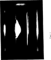
図2及び図4は図1a及び図1bに示された放電源の撮影写真を示す。この写真を説明するために、既に上記において採用した対応符号を利用する。両写真は長手軸線の方向に端部壁9を見てそれぞれ撮影された。両写真は電極形状だけが異なっている。条帯状電極3、4の幅ならびにそれらの相互間隔は第1の例ではそれぞれ3mm及び4mm、第2の例ではそれぞれ1mm及び10mmである。特に第1の例(図2、上側)では電極3、4ははっきり分かる。電極は暗領域として蓋5の壁から際立って見える。蓋5はガラスの反射された散乱蛍光のために底部6の対向位置する壁と同様に明るく見える。電極の長さはそれぞれ35mmである。両例において、特に第2の例(図4)においては、放電の固有光は両電極3、4間の領域では暗区域12によって蓋5の内壁から分離されていることが認められる。即ち、放電11は上記領域では内壁表面に対して距離を有している。放射源1の長手軸線の方向に見て、放電11はとい形又は横長の桶の形をした外観形状を有している(見る方向のために図2及び図4では認められない。図1a及び図1b参照)。
放射源が例えば電圧振幅を減少させることによって電力を少なく与えられると、連続なとい形の放電構造は幾つかの個別構造に引き裂かれる。しかしながら、これらの個別構造は図1aに示されるのと同様に、誘電体表面から際立って見える。個別構造は(目下の)陽極の方向にそれぞれ広がるデルタ状形状(Δ)を有している。両側誘電体妨害形放電の電圧パルスの交互極性の場合、2つのデルタ状構造の重なりが見える。
図3及び図5は図2及び図4による点灯中に電極で測定された電圧U(t)及び電流I(t)の時間変化を示す。両図を比較すると、電圧及び電流への電極形状の冒頭で述べた影響が証明される。次の表には最も重要な電気量がまとめられている。

図6a及び図6bには本発明による点灯に適した照明装置の横断面図及び(底部側を見た)平面図が概略的に示されている。この照明装置は放射源14と点灯時に放射源14に電圧パルス列を供給する電源27とを備えている。放射源14は、矩形状の底面を有する平坦状放電管15と、5つの条帯状電極16〜20とから構成されている。放電管15は矩形状底板21と浴槽の形をした蓋22とから構成されている。底板21及び蓋22はそれらを一巡する縁部の領域が気密に相互結合され、それにより放電源14の封入ガスを取囲んでいる。この封入ガスは10kPaの封入圧を持つキセノンから構成されている。電極16〜20は同じ幅を持ち、底板21の外壁上に互いに平行にかつ等間隔で設けられている。このことはそれぞれ隣接する電極間の全ての放電に対して同じ条件を保証するために重要である。これによって適切なパルス列の場合に最適な放射効率つまり輝度分布の一様性が達成される。このために電極16〜20は電源の両極23、24に交互に接続される。即ち、電極16と、この電極16に対して次の次の電極18と、この電極18に対して次の次の電極20とは電源の第1極23に接続される。それらの間にそれぞれ位置する両電極17、19は電源の第2極24に接続される。蓋22及び底板21の内壁上には発光体層25が噴射成形されており、この発光体層25はここには概略的に示された放電26の真空紫外線もしくは紫外線を(可視)光に変換する。TECHNICAL FIELD The present invention relates to a discharge tube made of a non-conductive material that is at least partially transparent and is enclosed with a sealed gas or closed or through which a gas or mixed gas flows, and a dielectric from each other and from the inside of the discharge tube. The present invention relates to an incoherent radiation source comprising an electrode separated by a material, in particular a method for lighting a discharge lamp with a dielectric disturbing discharge .
Furthermore, the present invention is a lighting device comprising a radiation source and a power source for applying a voltage to the radiation source, wherein the radiation source is at least partially transparent and sealed with an enclosed gas or gas Alternatively, it is composed of an open discharge tube made of non-conductive material through which mixed gas flows and electrodes connected to a power source separated from each other and from the inside of the discharge tube by a dielectric material, and radiation from the radiation source is incoherent. The radiation source relates to a lighting device suitable for dielectric disturbing discharge .
Incoherent radiation sources are to be understood as ultraviolet and infrared emitters and in particular discharge lamps that emit visible light.
Industrial applicability This type of radiation source, depending on the spectrum of emitted radiation, can be used for general and auxiliary lighting (eg residential and office lighting or background lighting of display devices (eg liquid crystal displays)), traffic and Suitable for signal illumination, ultraviolet irradiation (eg sterilization or photolysis) and infrared irradiation (eg resist drying).
Conventional technology
In WO 94/23442 pamphlet, incoherent source by dielectrically impeded discharge, describes a particular method of lighting a discharge lamp. This lighting method uses a voltage pulse train, in which case the individual voltage pulses are separated from one another by a pause time. The advantage of this pulse lighting method is the high efficiency of radiation generation.
An important drawback is that creeping discharges particularly heat the surface. Therefore, a cooling passage for discharging heat from the dielectric has also been proposed. The enormous heat generation that is unavoidable in this type of discharge limits the efficiency of radiation generation, particularly in the ultraviolet and vacuum ultraviolet regions. In addition, creeping discharges cause chemical phenomena on the surface, thereby shortening the lifetime of the radiator.
DISCLOSURE OF THE INVENTION An object of the present invention is to eliminate these drawbacks and to provide a method for lighting an incoherent radiation source characterized by a flat discharge tube and an efficient generation of radiation.
Such a problem is achieved according to the invention by a discharge tube made of a non-conductive material, which is at least partly transparent and closed with encapsulated gas or closed with a gas or mixed gas, and with each other and with the discharge. In a method of lighting an incoherent radiation source comprising an electrode separated from the interior of a tube by a dielectric material with a dielectric disturbing discharge, the electrodes are juxtaposed and alternately connected to electrodes of a power supply supplying a voltage pulse train, The individual voltage pulses are separated from each other by a dwell time, thereby generating a spatial discharge within the discharge tube having a distance from the inner wall surface of the discharge tube in the region between the electrodes of different polarity. Solved.
Other advantageous features of the method for lighting the incoherent radiation source are described in claims 2-11.
The other subject of this invention is providing the illuminating device suitable for this lighting method. According to the present invention, there is provided a lighting device comprising a radiation source and a power source for applying a voltage to the radiation source, wherein the radiation source is at least partially transparent and sealed with an enclosed gas. Or a non-conductive discharge tube made of a non-conductive material through which a gas or mixed gas flows, and electrodes separated from each other and from the inside of the discharge tube by a dielectric material and connected to a power source. Are emitted incoherently, the radiation source is suitable for dielectric disturbing discharge, the electrodes are juxtaposed and alternately connected to both poles of the power supply, the power supply can supply a voltage pulse train, and the individual voltage pulses are Each is separated from each other by a pause time, thereby generating a spatial discharge within the discharge tube having a distance from the inner wall surface of the discharge tube in the region between the electrodes of different polarities. It is solved by.
The basic idea of the present invention is that a spatial discharge is generated inside a discharge tube having juxtaposed dielectric electrodes, and the distance between the electrodes where the spatial discharge is opposite in polarity to the inner wall surface of the discharge tube. It is to have it. In the prior art, a large number of creeping discharges along the dielectric surface are used to generate ultraviolet rays, whereas the present invention proposes the use of a discharge that rises from the dielectric surface and spreads spatially inside the discharge tube.
The advantage obtained by this is, on the one hand, that the efficiency of UV or vacuum UV generation is high and therefore heat generation is minimal. Unlike the prior art, no cooling liquid is required for heat dissipation. On the other hand, in the discharge type according to the invention, the thermal and chemical tube wall load is clearly less than in the case of surface creeping discharge. As a result, the life of the discharge tube can be extended. Furthermore, according to the present invention, a luminance distribution that is more uniform, flat, and spatially dispersed can be realized between the electrodes. Such a luminance distribution provides a great advantage for photoimaging illumination or illumination, for example in the photolithography field, compared to tubular creeping discharges. The distributed luminance distribution here directly improves process efficiency. In this regard, a light emission pattern such as a conventional tubular light emitting structure is undesirable.
In the method according to the invention, the juxtaposed dielectric electrodes are connected to a power supply supplying a voltage pulse train. The individual voltage pulses are separated from one another by a pause time. Surprisingly, such a process generates highly efficient radiation, and also unexpectedly, inside the discharge tube, in the region between the electrodes of different polarities, on the inner wall surface of the discharge tube. It has been shown that a spatial discharge having a distance to it is generated.
Assuming repeated voltage pulses, the pulse width and pause time are set so that a spatial discharge according to the present invention partially lifted from the dielectric surface occurs. Typical pulse widths and pause times are in the range of 0.1 μs to 5 μs and in the range of 5 μs to 100 μs depending on the pulse repetition frequency in the range of 200 kHz to 10 kHz. Optimum values for pulse width and dwell time will depend on the specific discharge structure, ie the type and pressure of the encapsulated gas and the electrode structure in each instance. The electrode structure is given by the type and thickness of the dielectric, the area and shape of the electrode, and the electrode spacing. Depending on the discharge structure, the voltage signal to be applied is selected such that a discharge floating from the dielectric surface occurs and that discharge has the maximum radiation at the desired power density. In principle also suitable voltage pulse train as described in WO 94/23442 pamphlet. The height of the voltage pulse is generally about 100 V to 10 kV. The shape of the current pulse is determined by the voltage pulse shape and the discharge structure.
Suitable for the electrode structure are two or more elongated electrodes made of a conductive material (for example a metal wire or strip, or an elongated layer provided, for example, by vapor deposition on the outer surface of the discharge vessel wall). The electrodes are preferably arranged parallel to each other and at equal intervals. This is important to ensure the same conditions for all discharges between adjacent electrodes. This ensures uniform illumination over a large area. In addition, an optimum radiation efficiency can be obtained in this way with an appropriate pulse train. The lateral dimensions of the anode or cathode (ie, wire diameter or strip width) can be varied.
Lighting method according to the invention Many of the discharge tube shape, also suitable for all of the discharge tube shape described herein, especially in European Patent Application Publication No. 0363832. In that case, whether the discharge tube contains an enclosed gas, such as a discharge lamp, and is hermetically closed, or the discharge tube is open on both sides and the gas or mixed gas flows, for example, as in the case of a photolysis reactor Whether or not to do so is not important. The only important thing for the lighting mode is that the dielectric electrodes are juxtaposed. Here, “parallel” means that adjacent electrodes having different polarities are located on one side of the discharge area.
The electrodes can be arranged in one common plane, for example on the outer surface of the wall of the discharge vessel (auxiliarily covered with a dielectric protective layer if necessary) or directly embedded in the wall. Furthermore, the electrodes can also be arranged on different sides of the discharge area, in particular parallel to one another. For example, as described in German Patent Application No. 4036122, continuous electrodes with alternating polarities are arranged according to the polarity in one of two planes that are offset from each other.
In the case of a flat discharge tube, it is advantageous if the bottom or ceiling surface is used as a wall for arranging the electrodes. A flat radiation source is particularly suitable for large area flat illumination (eg background illumination of display panels or liquid crystal display screens) or illumination purposes (eg photolithography or resist curing).
In addition to flat discharge tubes , curved discharge tubes (eg tubular discharge tubes) are also suitable. A discharge tube which is open on both sides in a tubular shape and through which a gas or mixed gas flows is particularly suitable as a photolysis reactor. In its simplest configuration, the tubular discharge tube is formed, for example, by a dielectric tube having a circular cross section. In that case, the electrode is disposed on at least a portion of the outer surface of the tube or in at least a portion of the wall of the tube. A discharge is formed inside the tube during lighting. In a variant, the inner wall of the tube in the electrode region is provided with a dielectric layer used as a light reflector.
Another configuration of the tubular discharge tube consists of two concentric tubes with different diameters and electrodes arranged on or in the inner wall of the smaller diameter tube. A discharge is formed in the space between both tubes during lighting.
The inner wall of the discharge tube can be provided with a light emitter layer that converts discharge ultraviolet light or vacuum ultraviolet light into light. The variant with a luminescent layer that emits white light is particularly suitable for general illumination.
The selection of ionizable inclusions and, in some cases, the phosphor layer is tailored to the intended use. In particular, noble gases (eg, neon, argon, krypton, and xenon) and a mixture of noble gases are suitable. Of course, other encapsulating materials can also be used, and therefore all encapsulating materials normally used for light emission, in particular mercury, rare gas / mercury mixtures and rare earths and their halides can be used.
The illuminating device is completed by providing a power source that supplies the voltage pulse train when the output electrode is connected to the electrode of the discharge tube and is lit.
DESCRIPTION OF THE DRAWINGS The present invention will be described in detail below on the basis of several embodiments.
FIG. 1a is a cross-sectional view of a radiation source comprising two juxtaposed dielectric electrodes.
FIG. 1b is a longitudinal sectional view of the radiation source shown in FIG. 1a.
FIG. 2 is a front view of the radiation source of FIG. 1a lit according to the present invention.
FIG. 3 is a characteristic diagram showing temporal changes in the current I (t) and the voltage U (t) measured at the electrodes during lighting according to FIG.
FIG. 4 is a front view similar to FIG. 2 using a radiation source having a different electrode shape .
FIG. 5 is a diagram showing a part of the temporal change of the current I (t) and the voltage U (t) measured at the electrodes during lighting according to FIG.
FIG. 6a is a cross-sectional view of a lighting device suitable for lighting according to the present invention.
6b is a plan view of the illumination device of FIG. 6a.
1a and 1b schematically show a cross-sectional view and a longitudinal cross-sectional view of the
2 and 4 show a photograph of the discharge source shown in FIGS. 1a and 1b. In order to explain this photograph, the corresponding codes already adopted above are used. Both photographs were taken looking at the
If the radiation source is given less power, for example by reducing the voltage amplitude, the continuous cone-shaped discharge structure is torn into several individual structures. However, these individual structures are visible from the dielectric surface, similar to that shown in FIG. 1a. The individual structures have a delta shape (Δ) that extends in the direction of the (current) anode. In the case of alternating polarity of the voltage pulse of a double-sided dielectric disturbing discharge, an overlap of the two delta-like structures is visible.
3 and 5 show the time variation of voltage U (t) and current I (t) measured at the electrodes during lighting according to FIGS. Comparing the two figures demonstrates the effect described at the beginning of the electrode shape on voltage and current. The following table summarizes the most important quantities of electricity.
6a and 6b schematically show a cross-sectional view and a plan view (seen at the bottom side) of a lighting device suitable for lighting according to the present invention. This illuminating device includes a
Claims (12)
Applications Claiming Priority (3)
| Application Number | Priority Date | Filing Date | Title |
|---|---|---|---|
| DE19526211.5 | 1995-07-18 | ||
| DE19526211A DE19526211A1 (en) | 1995-07-18 | 1995-07-18 | Process for operating discharge lamps or emitters |
| PCT/DE1996/001317 WO1997004625A1 (en) | 1995-07-18 | 1996-07-18 | Method for operating a lighting system and suitable lighting system therefor |
Publications (2)
| Publication Number | Publication Date |
|---|---|
| JPH11509362A JPH11509362A (en) | 1999-08-17 |
| JP3856473B2 true JP3856473B2 (en) | 2006-12-13 |
Family
ID=7767155
Family Applications (1)
| Application Number | Title | Priority Date | Filing Date |
|---|---|---|---|
| JP50616597A Expired - Fee Related JP3856473B2 (en) | 1995-07-18 | 1996-07-18 | Incoherent radiation source lighting method and illumination device suitable therefor |
Country Status (11)
| Country | Link |
|---|---|
| US (1) | US5994849A (en) |
| EP (1) | EP0839436B1 (en) |
| JP (1) | JP3856473B2 (en) |
| KR (1) | KR100363751B1 (en) |
| CN (1) | CN1113582C (en) |
| CA (1) | CA2224362C (en) |
| DE (2) | DE19526211A1 (en) |
| HK (1) | HK1015114A1 (en) |
| HU (1) | HU223365B1 (en) |
| IN (1) | IN190521B (en) |
| WO (1) | WO1997004625A1 (en) |
Families Citing this family (48)
| Publication number | Priority date | Publication date | Assignee | Title |
|---|---|---|---|---|
| JP3264938B2 (en) | 1997-03-21 | 2002-03-11 | パテント―トロイハント―ゲゼルシヤフト フユア エレクトリツシエ グリユーランペン ミツト ベシユレンクテル ハフツング | Flat fluorescent lamp for backlight and liquid crystal display device provided with the flat fluorescent lamp |
| DE19711893A1 (en) * | 1997-03-21 | 1998-09-24 | Patent Treuhand Ges Fuer Elektrische Gluehlampen Mbh | Flat radiator |
| WO1998043276A2 (en) * | 1997-03-21 | 1998-10-01 | Patent-Treuhand-Gesellschaft für elektrische Glühlampen mbH | Gas discharge lamp with dielectrically impeded electrodes |
| DE19729175A1 (en) * | 1997-03-21 | 1999-01-14 | Patent Treuhand Ges Fuer Elektrische Gluehlampen Mbh | Flat radiator |
| DE19711892A1 (en) | 1997-03-21 | 1998-09-24 | Patent Treuhand Ges Fuer Elektrische Gluehlampen Mbh | Flat radiator |
| DE19734885C1 (en) * | 1997-08-12 | 1999-03-11 | Patent Treuhand Ges Fuer Elektrische Gluehlampen Mbh | Method for generating pulse voltage sequences for the operation of discharge lamps and associated circuit arrangement |
| EP0926705A1 (en) * | 1997-12-23 | 1999-06-30 | Patent-Treuhand-Gesellschaft für elektrische Glühlampen mbH | Flat radiator with locally modulated surface illumination density |
| EP0932185A1 (en) | 1997-12-23 | 1999-07-28 | Patent-Treuhand-Gesellschaft für elektrische Glühlampen mbH | Signal lamp and phosphor |
| EP0926704A1 (en) * | 1997-12-23 | 1999-06-30 | Patent-Treuhand-Gesellschaft für elektrische Glühlampen mbH | Flat signalling lamp with dielectric barrier discharge |
| DE19817480B4 (en) * | 1998-03-20 | 2004-03-25 | Patent-Treuhand-Gesellschaft für elektrische Glühlampen mbH | Flat lamp for dielectrically disabled discharges with spacers |
| DE19817476B4 (en) * | 1998-04-20 | 2004-03-25 | Patent-Treuhand-Gesellschaft für elektrische Glühlampen mbH | Fluorescent lamp with spacers and locally thinned fluorescent layer thickness |
| DE19817477A1 (en) | 1998-04-20 | 1999-10-21 | Patent Treuhand Ges Fuer Elektrische Gluehlampen Mbh | Fluorescent lamp |
| DE19826809A1 (en) * | 1998-06-16 | 1999-12-23 | Patent Treuhand Ges Fuer Elektrische Gluehlampen Mbh | Dielectric layer for discharge lamps and associated manufacturing process |
| DE19844725A1 (en) | 1998-09-29 | 2000-03-30 | Patent Treuhand Ges Fuer Elektrische Gluehlampen Mbh | Gas discharge lamp with controllable light length |
| DE19845228A1 (en) * | 1998-10-01 | 2000-04-27 | Patent Treuhand Ges Fuer Elektrische Gluehlampen Mbh | Dimmable discharge lamp for dielectric barrier discharges |
| JP2002540583A (en) * | 1999-03-25 | 2002-11-26 | コーニンクレッカ フィリップス エレクトロニクス エヌ ヴィ | Lighting equipment |
| JP3736201B2 (en) * | 1999-05-14 | 2006-01-18 | ウシオ電機株式会社 | Light source device |
| DE10016982A1 (en) * | 2000-04-06 | 2001-10-25 | Wedeco Ag | Method for feeding a UV light low pressure lamp and ballast for feeding a UV light low pressure lamp |
| US6541924B1 (en) * | 2000-04-14 | 2003-04-01 | Macquarie Research Ltd. | Methods and systems for providing emission of incoherent radiation and uses therefor |
| JP3471782B2 (en) * | 2001-02-13 | 2003-12-02 | Nec液晶テクノロジー株式会社 | Flat fluorescent lamp unit and liquid crystal display device using the same |
| US6762556B2 (en) | 2001-02-27 | 2004-07-13 | Winsor Corporation | Open chamber photoluminescent lamp |
| DE10122211A1 (en) | 2001-05-08 | 2002-11-14 | Patent Treuhand Ges Fuer Elektrische Gluehlampen Mbh | Flat lighting device with mirror surface |
| DE10134965A1 (en) * | 2001-07-23 | 2003-02-06 | Patent Treuhand Ges Fuer Elektrische Gluehlampen Mbh | Flat discharge lamp has outer side of front plate at least partly provided with opaque coating and inner side of front plate at least partly provided with fluorescent coating |
| DE10140355A1 (en) * | 2001-08-17 | 2003-02-27 | Patent Treuhand Ges Fuer Elektrische Gluehlampen Mbh | Discharge lamp with ignition aid |
| DE10236420A1 (en) * | 2002-08-08 | 2004-02-19 | Patent-Treuhand-Gesellschaft für elektrische Glühlampen mbH | Dielectric barrier discharge lamp comprises a discharge vessel enclosing a discharge medium, an electrode set, and a luminous material applied on a part of the wall of the vessel |
| WO2004016049A1 (en) * | 2002-08-08 | 2004-02-19 | Matsushita Electric Industrial Co., Ltd. | Light emitting element and production method therefor and display device |
| DE10324832A1 (en) * | 2003-06-02 | 2004-12-23 | Patent-Treuhand-Gesellschaft für elektrische Glühlampen mbH | Discharge lamp with fluorescent |
| DE10326755A1 (en) * | 2003-06-13 | 2006-01-26 | Patent-Treuhand-Gesellschaft für elektrische Glühlampen mbH | Discharge lamp with dual band phosphor |
| DE10347636A1 (en) * | 2003-10-09 | 2005-05-04 | Patent Treuhand Ges Fuer Elektrische Gluehlampen Mbh | Discharge lamp with at least one outer electrode and method for its production |
| KR101002321B1 (en) * | 2003-12-16 | 2010-12-20 | 엘지디스플레이 주식회사 | Apparatus and method for driving lamp of liquid crystal display device |
| DE102004020398A1 (en) * | 2004-04-23 | 2005-11-10 | Patent-Treuhand-Gesellschaft für elektrische Glühlampen mbH | Dielectric barrier discharge lamp with external electrodes and lighting system with this lamp |
| US7196473B2 (en) * | 2004-05-12 | 2007-03-27 | General Electric Company | Dielectric barrier discharge lamp |
| DE102004025266A1 (en) * | 2004-05-19 | 2005-12-08 | Patent-Treuhand-Gesellschaft für elektrische Glühlampen mbH | Lighting system with a housing and a flat lamp arranged therein |
| US7446477B2 (en) * | 2004-07-06 | 2008-11-04 | General Electric Company | Dielectric barrier discharge lamp with electrodes in hexagonal arrangement |
| US20060006804A1 (en) * | 2004-07-06 | 2006-01-12 | Lajos Reich | Dielectric barrier discharge lamp |
| DE102004039902B3 (en) * | 2004-08-17 | 2006-04-06 | Berger Gmbh | Flat gas discharge lamp, has flat plates forming dielectric layers with dielectrically restricted discharge |
| WO2006072892A2 (en) * | 2005-01-07 | 2006-07-13 | Philips Intellectual Property & Standards Gmbh | Segmented dielectric barrier discharge lamp |
| TWI285519B (en) * | 2005-11-04 | 2007-08-11 | Delta Electronics Inc | Method adopting square voltage waveform for driving flat lamps |
| DE102005034505A1 (en) | 2005-07-20 | 2007-02-01 | Patent-Treuhand-Gesellschaft für elektrische Glühlampen mbH | Circuit arrangement with transformerless converter with choke for the pulsed operation of dielectric barrier discharge lamps |
| TW200721907A (en) * | 2005-11-18 | 2007-06-01 | Delta Optoelectronics Inc | An improved startup method for the mercury-free flat-fluorescent lamp |
| US7495396B2 (en) * | 2005-12-14 | 2009-02-24 | General Electric Company | Dielectric barrier discharge lamp |
| TW200740300A (en) * | 2006-04-04 | 2007-10-16 | Delta Optoelectronics Inc | Driving circuit and method for fluorescent lamp |
| DE102006026332A1 (en) | 2006-06-02 | 2007-12-06 | Patent-Treuhand-Gesellschaft für elektrische Glühlampen mbH | Discharge lamp for dielectrically impeded discharges with rib-like support elements between base plate and ceiling plate |
| DE102006026333A1 (en) * | 2006-06-02 | 2007-12-06 | Patent-Treuhand-Gesellschaft für elektrische Glühlampen mbH | Discharge lamp for dielectrically impeded discharges with flat discharge vessel |
| DE102006050136B4 (en) * | 2006-10-25 | 2016-12-15 | Leibniz-Institut für Analytische Wissenschaften-ISAS-e.V. | Method and device for generating positive and / or negative ionized gas analytes for gas analysis |
| US20080174226A1 (en) | 2007-01-23 | 2008-07-24 | Nulight Technology Corporation | Mercury-free flat fluorescent lamps |
| DE102007006861B3 (en) * | 2007-02-12 | 2008-05-29 | Universität Karlsruhe (Th) | Radiation source for producing electromagnetic radiation having a first wavelength region comprises electrodes connected to an alternating voltage source, a gas-filled transparent discharge vessel and a dielectric layer |
| TWI362053B (en) * | 2008-04-30 | 2012-04-11 | Applied Green Light Taiwan Inc | Flat discharge lamp and the production method thereof |
Family Cites Families (16)
| Publication number | Priority date | Publication date | Assignee | Title |
|---|---|---|---|---|
| DE6753632U (en) * | 1968-09-19 | 1969-05-29 | Philips Nv | LOW PRESSURE DISCHARGE LAMP WITH A WALL NOT CLOSING THE DISCHARGE SPACE, THAT U.A. CONSISTS OF A BEAM. |
| US3648100A (en) * | 1969-03-24 | 1972-03-07 | Westinghouse Electric Corp | Electrodeless pulsed illuminator |
| DE2600592A1 (en) * | 1976-01-09 | 1977-07-21 | Onoda Cement Co Ltd | Producing charged powder particles - using parallel linear electrodes embedded in single planar insulator layer |
| US4427923A (en) * | 1981-10-01 | 1984-01-24 | Gte Laboratories Inc. | Electrodeless fluorescent light source |
| US4427924A (en) * | 1981-10-01 | 1984-01-24 | Gte Laboratories Inc. | Enhanced electrodeless light source |
| US4427922A (en) * | 1981-10-01 | 1984-01-24 | Gte Laboratories Inc. | Electrodeless light source |
| FR2520951A1 (en) * | 1982-02-04 | 1983-08-05 | Commissariat Energie Atomique | ELECTROMAGNETIC PULSE GENERATOR OF HIGH VOLTAGE |
| JPS60172135A (en) * | 1984-02-15 | 1985-09-05 | Mitsubishi Electric Corp | Flat plate light source |
| AU607520B2 (en) * | 1987-08-06 | 1991-03-07 | Shing Cheung Chow | Discharge lamp type display device |
| CH676168A5 (en) * | 1988-10-10 | 1990-12-14 | Asea Brown Boveri | |
| US5118989A (en) * | 1989-12-11 | 1992-06-02 | Fusion Systems Corporation | Surface discharge radiation source |
| DE69210113T2 (en) * | 1991-07-01 | 1996-11-21 | Philips Patentverwaltung | High pressure glow discharge lamp |
| US5561351A (en) * | 1992-10-14 | 1996-10-01 | Diablo Research Corporation | Dimmer for electrodeless discharge lamp |
| JP3075041B2 (en) * | 1992-12-28 | 2000-08-07 | 三菱電機株式会社 | Gas discharge display |
| DE4311197A1 (en) * | 1993-04-05 | 1994-10-06 | Patent Treuhand Ges Fuer Elektrische Gluehlampen Mbh | Method for operating an incoherently radiating light source |
| TW348262B (en) * | 1993-09-08 | 1998-12-21 | Ushio Electric Inc | Dielectric barrier discharge lamp |
-
1995
- 1995-07-18 DE DE19526211A patent/DE19526211A1/en not_active Ceased
-
1996
- 1996-07-16 IN IN1293CA1996 patent/IN190521B/en unknown
- 1996-07-18 HU HU0004552A patent/HU223365B1/en not_active IP Right Cessation
- 1996-07-18 WO PCT/DE1996/001317 patent/WO1997004625A1/en active IP Right Grant
- 1996-07-18 KR KR1019970709970A patent/KR100363751B1/en not_active IP Right Cessation
- 1996-07-18 DE DE59605924T patent/DE59605924D1/en not_active Expired - Lifetime
- 1996-07-18 EP EP96924752A patent/EP0839436B1/en not_active Expired - Lifetime
- 1996-07-18 CN CN96195613A patent/CN1113582C/en not_active Expired - Fee Related
- 1996-07-18 US US08/983,113 patent/US5994849A/en not_active Expired - Lifetime
- 1996-07-18 CA CA002224362A patent/CA2224362C/en not_active Expired - Fee Related
- 1996-07-18 JP JP50616597A patent/JP3856473B2/en not_active Expired - Fee Related
-
1999
- 1999-01-06 HK HK99100023A patent/HK1015114A1/en not_active IP Right Cessation
Also Published As
| Publication number | Publication date |
|---|---|
| CA2224362C (en) | 2004-04-13 |
| HUP0004552A2 (en) | 2001-04-28 |
| WO1997004625A1 (en) | 1997-02-06 |
| KR19990028648A (en) | 1999-04-15 |
| US5994849A (en) | 1999-11-30 |
| DE59605924D1 (en) | 2000-10-26 |
| CN1113582C (en) | 2003-07-02 |
| IN190521B (en) | 2003-08-09 |
| HU223365B1 (en) | 2004-06-28 |
| KR100363751B1 (en) | 2003-02-19 |
| JPH11509362A (en) | 1999-08-17 |
| HUP0004552A3 (en) | 2003-07-28 |
| CA2224362A1 (en) | 1997-02-06 |
| DE19526211A1 (en) | 1997-01-23 |
| HK1015114A1 (en) | 1999-10-08 |
| EP0839436B1 (en) | 2000-09-20 |
| CN1191061A (en) | 1998-08-19 |
| EP0839436A1 (en) | 1998-05-06 |
Similar Documents
| Publication | Publication Date | Title |
|---|---|---|
| JP3856473B2 (en) | Incoherent radiation source lighting method and illumination device suitable therefor | |
| US6060828A (en) | Electric radiation source and irradiation system with this radiation source | |
| JP3715231B2 (en) | Method of operating an incoherent emission source | |
| KR100503466B1 (en) | Cold cathode for discharge lamps, discharge lamp fitted with said cold cathode, and principle of operation of said discharge lamp | |
| US5965988A (en) | Discharge lamp with galvanic and dielectric electrodes and method | |
| KR101949001B1 (en) | Gas discharge device for ultraviolet light emission, planar light source using same, and method for driving same | |
| JP2000513872A (en) | Fluorescent lamp | |
| JP3037441B2 (en) | Flat light emitter | |
| JP4783074B2 (en) | Dielectric barrier discharge lamp | |
| JP3249538B2 (en) | Flat light emitter | |
| KR100330087B1 (en) | Flat type lamp using the plasma cathode | |
| EP0948030A2 (en) | Rare gaseous discharge lamp, lighting circuit, and lighting device | |
| KR100307445B1 (en) | Surface light source device | |
| JPH05190150A (en) | Electric discharge lamp | |
| KR20030045540A (en) | A platelike electrodeless fluorescent lamp having linear micro hollow cathodes | |
| JPH0330259B2 (en) | ||
| JP2000277056A (en) | Rare gas discharge lamp, rare gas discharge lamp lighting device and lighting system | |
| KR100739540B1 (en) | High efficient light source by using multi electrode | |
| JPH09219178A (en) | Discharge tube | |
| JPH04237943A (en) | Surface luminescence type light source device and driving method thereof | |
| JPH11329364A (en) | Ultraviolet ray generation device | |
| JPH08185824A (en) | Discharge lamp device and lighting system | |
| JPH06314562A (en) | Fluorescent lamp and manufacture thereof | |
| KR980013533A (en) | Flat lamp type light source | |
| JP2002313284A (en) | Fluorescent lamp and illumination device |
Legal Events
| Date | Code | Title | Description |
|---|---|---|---|
| A131 | Notification of reasons for refusal |
Free format text: JAPANESE INTERMEDIATE CODE: A131 Effective date: 20051122 |
|
| A521 | Request for written amendment filed |
Free format text: JAPANESE INTERMEDIATE CODE: A523 Effective date: 20060207 |
|
| A131 | Notification of reasons for refusal |
Free format text: JAPANESE INTERMEDIATE CODE: A131 Effective date: 20060328 |
|
| A521 | Request for written amendment filed |
Free format text: JAPANESE INTERMEDIATE CODE: A523 Effective date: 20060627 |
|
| TRDD | Decision of grant or rejection written | ||
| A01 | Written decision to grant a patent or to grant a registration (utility model) |
Free format text: JAPANESE INTERMEDIATE CODE: A01 Effective date: 20060815 |
|
| A61 | First payment of annual fees (during grant procedure) |
Free format text: JAPANESE INTERMEDIATE CODE: A61 Effective date: 20060912 |
|
| R150 | Certificate of patent or registration of utility model |
Free format text: JAPANESE INTERMEDIATE CODE: R150 |
|
| FPAY | Renewal fee payment (event date is renewal date of database) |
Free format text: PAYMENT UNTIL: 20090922 Year of fee payment: 3 |
|
| FPAY | Renewal fee payment (event date is renewal date of database) |
Free format text: PAYMENT UNTIL: 20100922 Year of fee payment: 4 |
|
| FPAY | Renewal fee payment (event date is renewal date of database) |
Free format text: PAYMENT UNTIL: 20110922 Year of fee payment: 5 |
|
| FPAY | Renewal fee payment (event date is renewal date of database) |
Free format text: PAYMENT UNTIL: 20110922 Year of fee payment: 5 |
|
| FPAY | Renewal fee payment (event date is renewal date of database) |
Free format text: PAYMENT UNTIL: 20120922 Year of fee payment: 6 |
|
| FPAY | Renewal fee payment (event date is renewal date of database) |
Free format text: PAYMENT UNTIL: 20130922 Year of fee payment: 7 |
|
| LAPS | Cancellation because of no payment of annual fees |