JP3856232B2 - Delay time correction circuit, video data processing circuit, and flat display device - Google Patents
Delay time correction circuit, video data processing circuit, and flat display device Download PDFInfo
- Publication number
- JP3856232B2 JP3856232B2 JP2003347803A JP2003347803A JP3856232B2 JP 3856232 B2 JP3856232 B2 JP 3856232B2 JP 2003347803 A JP2003347803 A JP 2003347803A JP 2003347803 A JP2003347803 A JP 2003347803A JP 3856232 B2 JP3856232 B2 JP 3856232B2
- Authority
- JP
- Japan
- Prior art keywords
- data
- logic level
- delay time
- circuit
- period
- Prior art date
- Legal status (The legal status is an assumption and is not a legal conclusion. Google has not performed a legal analysis and makes no representation as to the accuracy of the status listed.)
- Expired - Fee Related
Links
Images


Classifications
-
- G—PHYSICS
- G09—EDUCATION; CRYPTOGRAPHY; DISPLAY; ADVERTISING; SEALS
- G09G—ARRANGEMENTS OR CIRCUITS FOR CONTROL OF INDICATING DEVICES USING STATIC MEANS TO PRESENT VARIABLE INFORMATION
- G09G3/00—Control arrangements or circuits, of interest only in connection with visual indicators other than cathode-ray tubes
- G09G3/20—Control arrangements or circuits, of interest only in connection with visual indicators other than cathode-ray tubes for presentation of an assembly of a number of characters, e.g. a page, by composing the assembly by combination of individual elements arranged in a matrix no fixed position being assigned to or needed to be assigned to the individual characters or partial characters
- G09G3/34—Control arrangements or circuits, of interest only in connection with visual indicators other than cathode-ray tubes for presentation of an assembly of a number of characters, e.g. a page, by composing the assembly by combination of individual elements arranged in a matrix no fixed position being assigned to or needed to be assigned to the individual characters or partial characters by control of light from an independent source
- G09G3/36—Control arrangements or circuits, of interest only in connection with visual indicators other than cathode-ray tubes for presentation of an assembly of a number of characters, e.g. a page, by composing the assembly by combination of individual elements arranged in a matrix no fixed position being assigned to or needed to be assigned to the individual characters or partial characters by control of light from an independent source using liquid crystals
- G09G3/3611—Control of matrices with row and column drivers
- G09G3/3685—Details of drivers for data electrodes
-
- G—PHYSICS
- G09—EDUCATION; CRYPTOGRAPHY; DISPLAY; ADVERTISING; SEALS
- G09G—ARRANGEMENTS OR CIRCUITS FOR CONTROL OF INDICATING DEVICES USING STATIC MEANS TO PRESENT VARIABLE INFORMATION
- G09G3/00—Control arrangements or circuits, of interest only in connection with visual indicators other than cathode-ray tubes
- G09G3/20—Control arrangements or circuits, of interest only in connection with visual indicators other than cathode-ray tubes for presentation of an assembly of a number of characters, e.g. a page, by composing the assembly by combination of individual elements arranged in a matrix no fixed position being assigned to or needed to be assigned to the individual characters or partial characters
- G09G3/34—Control arrangements or circuits, of interest only in connection with visual indicators other than cathode-ray tubes for presentation of an assembly of a number of characters, e.g. a page, by composing the assembly by combination of individual elements arranged in a matrix no fixed position being assigned to or needed to be assigned to the individual characters or partial characters by control of light from an independent source
- G09G3/36—Control arrangements or circuits, of interest only in connection with visual indicators other than cathode-ray tubes for presentation of an assembly of a number of characters, e.g. a page, by composing the assembly by combination of individual elements arranged in a matrix no fixed position being assigned to or needed to be assigned to the individual characters or partial characters by control of light from an independent source using liquid crystals
-
- G—PHYSICS
- G09—EDUCATION; CRYPTOGRAPHY; DISPLAY; ADVERTISING; SEALS
- G09G—ARRANGEMENTS OR CIRCUITS FOR CONTROL OF INDICATING DEVICES USING STATIC MEANS TO PRESENT VARIABLE INFORMATION
- G09G2300/00—Aspects of the constitution of display devices
- G09G2300/04—Structural and physical details of display devices
- G09G2300/0404—Matrix technologies
- G09G2300/0408—Integration of the drivers onto the display substrate
Description
本発明は、遅延時間補正回路、ビデオデータ処理回路及びフラットディスプレイ装置に関し、例えば絶縁基板上に駆動回路を一体に形成した液晶表示装置に適用することができる。本発明は、入力データにダミーデータを介挿して入力データの論理レベルを強制的に切り換えることにより、TFT等による論理回路において遅延時間の変化を有効に回避することができるようにする。 The present invention relates to a delay time correction circuit, a video data processing circuit, and a flat display device, and can be applied to, for example, a liquid crystal display device in which a drive circuit is integrally formed on an insulating substrate. According to the present invention, a change in delay time can be effectively avoided in a logic circuit such as a TFT by forcibly switching the logic level of the input data by inserting dummy data into the input data.
近年、例えばPDA、携帯電話等の携帯端末装置に適用されるフラットディスプレイ装置である液晶表示装置においては、液晶表示パネルを構成する絶縁基板であるガラス基板上に、液晶表示パネルの駆動回路を一体に集積化して構成するものが提供されるようになされている。 In recent years, in a liquid crystal display device which is a flat display device applied to a portable terminal device such as a PDA or a mobile phone, a driving circuit for the liquid crystal display panel is integrated on a glass substrate which is an insulating substrate constituting the liquid crystal display panel. What is integrated and configured is provided.
すなわちこの種の液晶表示装置は、液晶セルと、この液晶セルのスイッチング素子である低温ポリシリコンTFT(Thin Film Transistor;薄膜トランジスタ)と、保持容量とによる画素をマトリックス状に配置して表示部が形成され、この表示部の周囲に配置した各種の駆動回路により表示部を駆動して各種の画像を表示するようになされている。 That is, in this type of liquid crystal display device, a display unit is formed by arranging liquid crystal cells, low-temperature polysilicon TFTs (thin film transistors) that are switching elements of the liquid crystal cells, and storage capacitors in a matrix. The display unit is driven by various drive circuits arranged around the display unit to display various images.
このような液晶表示装置においては、例えば順次ラスタ走査順に入力されてなる各画素の階調を示す階調データを奇数列及び偶数列の階調データに分離し、これら奇数列及び偶数列の階調データに基づいて、それぞれ表示部の上下に設けた奇数列用及び偶数列用の水平駆動回路で表示部を駆動することにより、表示部における配線パターンを効率良くレイアウトして高精細に画素を配置するようになされている。 In such a liquid crystal display device, for example, the gradation data indicating the gradation of each pixel inputted in the order of raster scanning is separated into the gradation data of the odd-numbered column and the even-numbered column, and the levels of these odd-numbered column and even-numbered column are separated. Based on the tone data, the display unit is driven by the horizontal drive circuits for odd columns and even columns respectively provided above and below the display unit, thereby efficiently laying out the wiring pattern in the display unit and arranging the pixels with high definition. It is made to arrange.
このように各水平駆動回路における階調データの処理においては、液晶表示装置に入力する階調データの配列との関係で、例えば特開平10−17371号公報、特開平10−177368号公報等に、種々の工夫が提案されるようになされている。 As described above, in the processing of gradation data in each horizontal drive circuit, for example, in Japanese Patent Laid-Open Nos. 10-17371 and 10-177368, etc. in relation to the arrangement of the gradation data input to the liquid crystal display device. Various ideas have been proposed.
このような液晶表示装置に適用される低温ポリシリコンTFTによるこの種の論理回路においては、長期間、入力値がLレベルに保持されると、続く論理レベルの立ち上がりの応答において遅延時間が長くなり、これにより直前の論理レベルの長さに応じて遅延時間が変化する問題がある。 In this type of logic circuit using a low-temperature polysilicon TFT applied to such a liquid crystal display device, if the input value is held at the L level for a long time, the delay time becomes long in the response of the subsequent rise of the logic level. As a result, there is a problem that the delay time changes according to the length of the immediately preceding logic level.
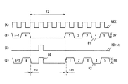
すなわち図11及び図12に示すようにこの種の論理回路において、例えば、メインクロックMCK(図12(A))に同期した入力データD1(図12(B))をレベルシフタ1に入力し、0〜3〔V〕による振幅を0〜6〔V〕に変換して出力する場合に、入力データD1の論理レベルがデユーティー比50〔%〕により切り換わっている期間T1において、遅延時間tdは、ほぼ一定となる。これに対して期間T2により示すように、入力データD1の論理レベルがLレベルに長時間保持されると、直後の遅延時間td1においては、期間T1における遅延時間tdより長くなる(図12(C))。
That is, as shown in FIGS. 11 and 12, in this type of logic circuit, for example, input data D1 (FIG. 12B) synchronized with the main clock MCK (FIG. 12A) is input to the
これにより図13に示すように、階調データの各ビットD1(図13(B1)及び(B2))をレベルシフトさせてサブクロックSCK(図13(A))によりラッチする場合に、この階調データが高転送速度によるデータの場合、この階調データの各ビットD1において論理レベルがデユーティー比50〔%〕により切り換わっている期間T1においては、このサブクロックSCKにより正しくレベルシフタ1の出力データD2Aをラッチできるのに対し(図13(B1)及び(C1))、例えば垂直ブランキング期間VBLの直後においては、正しくレベルシフタ1の出力データD2をラッチできなくなる(図13(B2)及び(C2))。
As a result, as shown in FIG. 13, when each bit D1 (FIG. 13 (B1) and (B2)) of the gradation data is level-shifted and latched by the sub clock SCK (FIG. 13 (A)), this level is used. When the tone data is data at a high transfer speed, the output data of the
このように正しくデータをラッチできない場合、液晶表示装置においては、上述したように、階調データを偶数列と奇数列とに分離して高解像度の表示部を駆動する場合、垂直ブランキング期間の直後において、局所的に誤った階調により画素を駆動することになる。また例えば黒色の背景の中にウィンドウ形状により白色の領域を表示する場合に、この白色の領域の走査開始端側でも、同様に誤った階調により画素を駆動することになる。また液晶表示装置においては、このような階調データD1が表示部の階調数に対応する例えば6ビットパラレルにより入力され、このような遅延時間の変化においては、階調データの各ビットで発生することにより、階調データの特定ビットだけ誤ったデータをラッチする場合も発生し、これらにより表示に供する画像によっては、著しく見苦しくなる。
本発明は以上の点を考慮してなされたもので、TFT等による論理回路において遅延時間の変化を有効に回避することができる遅延時間補正回路、このような遅延時間補正回路によるビデオデータ処理回路及びフラットディスプレイ装置を提案しようとするものである。 The present invention has been made in consideration of the above points. A delay time correction circuit capable of effectively avoiding a change in delay time in a logic circuit such as a TFT, and a video data processing circuit using such a delay time correction circuit. And a flat display device.
かかる課題を解決するため請求項1の発明においては、遅延時間補正回路に適用して、一定の周期で、一定期間の間、一定の論理レベルに保持される休止期間を有する入力データを処理するデータ処理回路に対して、休止期間の間の所定のタイミングで、入力データに一定の論理レベルとは逆の論理レベルによるダミーデータを介挿する。
In order to solve such a problem, the invention of
また請求項2の発明においては、一定の周期で、一定期間の間、一定の論理レベルに保持される休止期間を有する入力データを処理するデータ処理回路に適用して、休止期間の間の所定のタイミングで、入力データに一定の論理レベルとは逆の論理レベルによるダミーデータを介挿する。 According to a second aspect of the present invention, the present invention is applied to a data processing circuit that processes input data having a pause period that is held at a constant logic level for a fixed period and at a fixed period, and a predetermined period during the pause period. At this timing, dummy data having a logic level opposite to a certain logic level is inserted in the input data.
また請求項4の発明においては、フラットディスプレイ装置に適用して、階調データの水平ブランキング期間の間の所定のタイミングで、階調データに水平ブランキング期間の論理レベルとは逆の論理レベルによるダミーデータを介挿して階調データを処理する。 According to a fourth aspect of the present invention, when applied to a flat display device, the gradation data has a logical level opposite to the logical level of the horizontal blanking period at a predetermined timing during the horizontal blanking period of the gradation data. The gradation data is processed by interposing the dummy data.
請求項1の構成により、遅延時間補正回路に適用して、一定の周期で、一定期間の間、一定の論理レベルに保持される休止期間を有する入力データを処理するデータ処理回路に対して、休止期間の間の所定のタイミングで、入力データに一定の論理レベルとは逆の論理レベルによるダミーデータを介挿すれば、何らダミーデータを介挿しない場合に比して、続く論理レベルの変化における遅延時間を短くし得、その分、TFT等による論理回路において遅延時間の変化を有効に回避することができる。
According to the configuration of
これにより請求項2、請求項4の構成によれば、TFT等による論理回路において遅延時間の変化を有効に回避して、この遅延時間の変化による各種影響を有効に回避してデータ処理し得、また所望の画像を表示することができる。
Thus, according to the configurations of
本発明によれば、TFT等による論理回路において遅延時間の変化を有効に回避することができるビデオデータ処理回路及びフラットディスプレイ装置を提供することができる。 ADVANTAGE OF THE INVENTION According to this invention, the video data processing circuit and flat display apparatus which can avoid effectively the change of delay time in the logic circuit by TFT etc. can be provided.
以下、適宜図面を参照しながら本発明の実施例を詳述する。 Hereinafter, embodiments of the present invention will be described in detail with reference to the drawings as appropriate.
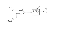
(1)遅延時間補正原理
図1は、図11との対比により本発明に係る遅延時間補正原理の説明に供するブロック図である。この補正原理においては、一定の周期で、一定期間の間、一定の論理レベルに保持される入力データを処理するデータ処理回路に対して、この一定の論理レベルに保持される期間の間の所定のタイミングで、この一定の論理レベルとは逆の論理レベルによるダミーデータを入力データに介挿する。なおここでこのように一定の周期で、一定期間の間、一定の論理レベルに保持される期間は、例えばビデオデータにおける水平ブランキング期間のように、有意なデータの伝送に供していない期間であり、以下においては、この期間を適宜、休止期間と呼ぶ。
(1) Delay time
すなわちこのデータ処理回路が例えばレベルシフタ1であって、図2に示すように、メインクロックMCK(図2(A))に同期した階調データD1を振幅0〜3〔V〕から振幅0〜6〔V〕に補正して出力データD2を出力する場合に(図2(B)及び(D))、この階調データD1が一定の周期で、一定期間の間、一定の論理レベルに保持される水平ブランキング期間T2の間、論理Lレベルから立ち上がるダミーデータDDを階調データD1に介挿する。このため例えばオア回路4を介して、このダミーデータDDによるリセットパルスHDrstを階調データD1に介挿する(図2(C))。
That is, this data processing circuit is, for example, a
これによりこの補正原理においては、何らダミーデータDDを介挿しない場合に比して、この水平ブランキング期間T2の直後の論理レベルの立ち上がりにおける遅延時間td1を短くするようになされ、直前の論理レベルの長さに応じて遅延時間が変化する問題を解決するようになされている。すなわちこのようにダミーデータDDを介挿すれば、強制的に入力データの論理レベルに切り換えて、何らダミーデータDDを介挿しない場合に比して、入力データの論理レベルを論理Lレベルに保持する期間を短くすることができ、その分、この入力データD1によるデータ列において、遅延時間の変動を少なくすることができる。従ってその分、誤ったデータのラッチ等を有効に回避することができる。 As a result, in this correction principle, the delay time td1 at the rise of the logic level immediately after the horizontal blanking period T2 is shortened as compared with the case where no dummy data DD is inserted, and the immediately preceding logic level is reduced. The problem is that the delay time varies depending on the length of the signal. That is, if the dummy data DD is inserted in this way, the logic level of the input data is forcibly switched to hold the logic level of the input data at the logic L level as compared with the case where no dummy data DD is inserted. The period during which the data is input can be shortened, and accordingly, the fluctuation of the delay time can be reduced in the data string based on the input data D1. Accordingly, erroneous data latching and the like can be effectively avoided.
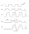
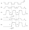
すなわち図13との対比により図3に示すように、このような論理回路出力をサブクロックSCK(図3(A))でサンプリングする場合にあっても、垂直ブランキング期間VBLの間の水平ブランキング期間でダミーデータDDが介挿されていることにより、垂直ブランキング期間VBLに続く論理レベルの立ち上がりにおける出力データD2の遅延時間を短くし得、有効映像期間における場合と同様のタイミングにより出力データD2をサンプリングしてラッチすることができ(図3(B1)〜(C2))、これにより垂直ブランキング期間VBLの立ち上がりに対応する画素を正しい階調により表示することができる。また黒レベルが数ライン連続して白レベルに立ち上がるような場合、さらには複数ビットの特定ビットが数ライン連続してLレベルに保持されて立ち上がるような場合でも、正しく入力データD1をラッチし得、これにより液晶表示装置に適用して各画素の階調を正しく表示することができる。 That is, as shown in FIG. 3 for comparison with Figure 1 3, even such a logic circuit output when sampling at sub clock SCK (FIG. 3 (A)), the horizontal during the vertical blanking period VBL Since the dummy data DD is inserted in the blanking period, the delay time of the output data D2 at the rise of the logic level following the vertical blanking period VBL can be shortened, and output at the same timing as in the effective video period. The data D2 can be sampled and latched (FIG. 3 (B1) to (C2)), whereby the pixel corresponding to the rising edge of the vertical blanking period VBL can be displayed with the correct gradation. Further, even when the black level rises to the white level continuously for several lines, or even when a specific bit of a plurality of bits rises while being held for several lines continuously, the input data D1 can be correctly latched. Thus, the gradation of each pixel can be correctly displayed when applied to a liquid crystal display device.
ところで図12について上述した遅延時間の変化においては、入力データD1が長時間論理Lレベルに保持された直後に、論理レベルが立ち上がった場合に、この立ち上がった論理レベルの立ち下がりが遅延するものである。しかしながらこのような論理レベルの立
ち上がりのタイミングを詳細に検討したところ、入力データD1が長時間論理Lレベルに保持された場合、立ち上がりのタイミングにあっては、図11との対比により図4に示すように、立ち下がりのタイミングとは逆に、遅延時間が短くなることが判った(図4(A)〜(C2))。これにより入力データD1をサンプリングするタイミングが、論理レベルが切り換わる直前に設定されている場合であって、サンプリングに係る位相余裕が少ない場合、この立ち上がりのタイミングに係る遅延時間の変化によっても、データを正しく処理できなくなる。
Meanwhile the change in delay time described above with reference to FIG. 1. 2, which input data D1 is immediately held in the logic L level for a long time, when the rise of the logic level, the fall of the upstanding logic level is delayed It is. However, when the rise timing of such a logic level is examined in detail, when the input data D1 is held at the logic L level for a long time, the rise timing is shown in FIG. 4 in comparison with FIG. Thus, it was found that the delay time is shortened contrary to the fall timing (FIGS. 4A to 4C). As a result, when the timing of sampling the input data D1 is set immediately before the logic level is switched and the phase margin related to sampling is small, the data is also detected by the change in the delay time related to the rising timing. Cannot be processed correctly.
しかしながらこのような設定に係る場合でも、この補正原理に係るように休止期間にダミーデータを介挿すれば、このような立ち上がりに係る遅延時間の減少する方向への遅延時間の変化についても補正することができ、これにより例えば液晶表示装置に適用して各画素の階調を正しく補正することができる。 However, even in such a setting, if dummy data is inserted in the pause period as in this correction principle, the change in the delay time in the direction in which the delay time related to the rise decreases is corrected. Thus, the gradation of each pixel can be corrected correctly when applied to, for example, a liquid crystal display device.
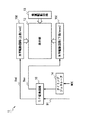
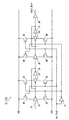
(2)実施例の構成
図5は、本発明の実施例に係る液晶表示装置を示すブロック図である。この液晶表示装置11においては、この図5に示す各駆動回路が表示部12の絶縁基板であるガラス基板上に一体に作成され、後述する水平駆動回路、タイミングジェネレータ等の駆動回路においては、低温ポリシリコンによるTFTにより作成される。
(2) Configuration of Embodiment FIG. 5 is a block diagram showing a liquid crystal display device according to an embodiment of the present invention. In the liquid
ここで表示部12は、液晶セルと、この液晶セルのスイッチング素子であるTFTと、保持容量とにより各画素が形成され、この各画素をマトリックス状に配置して矩形形状により形成される。
Here the
垂直駆動回路13は、タイミングジェネレータ14から出力される各種タイミング信号により、この表示部12のゲート線を駆動し、これによりライン単位で表示部12に設けられた画素を順次選択する。水平駆動回路15O及び15Eは、それぞれ表示部12の上下に設けられ、シリアルパラレル(SP)変換回路16から出力される奇数列及び偶数列の階調データDod及びDevを順次循環的にラッチした後、各ラッチ出力をディジタルアナログ変換処理し、その結果得られる駆動信号により表示部12の各信号線を駆動する。これにより水平駆動回路15O及び15Eは、それぞれ表示部12の奇数列及び偶数列の信号線を駆動し、垂直駆動回路13で選択された各画素を階調データDod及びDevに応じた階調に設定する。
The
タイミングジェネレータ14は、この液晶表示装置11の上位の装置から供給される各種基準信号より、この液晶表示装置11の動作に必要な各種タイミング信号を生成して出力する。シリアルパラレル変換回路16は、この液晶表示装置11の上位の装置から出力される階調データD1を奇数列及び偶数列の階調データDod及びDevに分離して出力する。ここで階調データD1は、各画素の階調を示すデータであり、表示部12の画素の配列に対応する赤色、青色、緑色の色データのラスタ走査順の連続によるビデオデータにより形成されるようになされている。
The
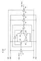
図6は、このシリアルパラレル変換回路16を関連する構成を共に示すブロック図である。このシリアルパラレル変換回路16は、0〜3〔V〕による階調データD1の振幅をレベルシフタ21により0〜6〔V〕の振幅に変換した後、ラッチ回路22、23により交互にラッチして奇数列及び偶数列の階調データDod及びDevに分離し、ダウンコンバータ24、25により元の振幅に戻して出力する。これによりシリアルパラレル変換回路16は、レベルシフタ21によるレベルシフトにより階調データD1の振幅を拡大して処理して、高転送レートによる階調データD1を確実に2系統の階調データに分離するようになされている。
FIG. 6 is a block diagram showing a configuration related to the serial-
この階調データD1に係る処理において、シリアルパラレル変換回路16は、レベルシフタ21の出力段にオア回路27が設けられ、このオア回路27により階調データD1の水平ブランキング期間で、階調データD1にダミーデータDDが介挿される。これによりこの液晶表示装置11では、階調データD1が長時間Lレベルに保持されることによる遅延時間の変化を防止し、続くラッチ回路22、23において、正しく階調データD1をラッチできるようになされている。なおこの液晶表示装置11では、レベルシフタ21で発生する遅延時間の変化だけでは、誤って階調データD1をラッチしないことにより、このようにレベルシフタ21の出力段において、ダミーデータDDを介挿するようになされている。
In the processing related to the gradation data D1, the serial-
このためタイミングジェネレータ(TG)14においては、各水平ブランキングの期間の間で信号レベルが立ち上がるリセットパルスHDrstを出力してオア回路27に供給するようになされている。
For this reason, the timing generator (TG) 14 outputs a reset pulse HDrst whose signal level rises during each horizontal blanking period and supplies it to the
図7は、ラッチ回路22を示す接続図である。ラッチ回路22及び23においては、ラッチのタイミングを制御するサンプリングパルスsp及びxspがそれぞれタイミングジェネレータ14から供給される点を除いて同一に構成されることにより、以下においては、ラッチ回路22についてのみ構成を説明し、ラッチ回路23については説明を省略する。またリセットパルスrstに係る処理については、記載を省略して示す。
FIG. 7 is a connection diagram showing the
このラッチ回路22においては、サンプリングパルスspをインバータ31に入力し、このサンプリングパルスspの反転信号を生成する。ラッチ回路22は、このサンプリングパルスspによりオン状態に切り換わるPチャンネルMOS(以下、PMOSと呼ぶ)トランジスタQ1、インバータ31より出力されるラッチパルスspの反転信号によりオン状態に切り換わるNチャンネルMOS(以下、NMOSと呼ぶ)トランジスタQ2によりそれぞれ正側及び負側電源VDD及びVSSに接続されてなるインバータ32に階調データD1が入力される。またそれぞれサンプリングパルスspの反転信号によりオン状態に切り換わるPチャンネルMOSトランジスタQ3、サンプリングパルスspによりオン状態に切り換わるNチャンネルMOSトランジスタQ4により正側及び負側電源VDD及びVSSに接続されてなるインバータ33の出力と、インバータ32の出力とが接続され、これらインバータ33、32の出力が、インバータ33と入力を共通に接続してなるインバータ34に接続される。これによりラッチ回路22は、ラッチセルを構成し、サンプリングパルスspにより階調データD1をラッチするようになされている。
In the
またラッチ回路22においては、それぞれサンプリングパルスspの反転信号によりオン状態に切り換わるPチャンネルMOSトランジスタQ5、サンプリングパルスspによりオン状態に切り換わるNチャンネルMOSトランジスタQ6により正側及び負側電源VDD及びVSSに接続されてなるインバータ35にインバータ34の出力が供給される。またサンプリングパルスspによりオン状態に切り換わるPチャンネルMOSトランジスタQ7、サンプリングパルスspの反転信号によりオン状態に切り換わるNチャンネルMOSトランジスタQ8によりそれぞれ正側及び負側電源VDD及びVSSに接続されてなるインバータ36の出力と、インバータ35の出力とが接続され、これらインバータ35、36の出力が、インバータ36と入力を共通に接続してなるインバータ37の出力に接続される。ラッチ回路22は、このインバータ37の出力がバッファ38を介して出力される。これによりラッチ回路22は、階調データD1をそれぞれ奇数列及び偶数列により分離してなる振幅0〜6〔V〕の階調データDod1及びDev1を出力するようになされている。
In the
図8は、ダウンコンバータ24を示す接続図である。ダウンコンバータ24、25は、処理対象のデータが異なる点を除いて同一に構成されることにより、以下においては、ダウンコンバータ24についてのみ構成を説明し、ダウンコンバータ25については説明を省略する。
FIG. 8 is a connection diagram showing the
このダウンコンバータ24は、6〔V〕の正側電源VDD2及び0〔V〕の負側電源VSSにより動作するインバータ41、このインバータ41の負側レベルを−3〔V〕に立ち下げるレベルシフタ42、6〔V〕の正側電源VDD2及び−3〔V〕の負側電源VSS2により動作してこのレベルシフタ42の出力のバッファリングして出力するインバータ43及び44の直列回路、3〔V〕の正側電源VDD1及び0〔V〕の負側電源VSSにより動作してインバータ44の出力の反転信号を出力するインバータ45により構成され、これらにより奇数列及び偶数列の階調データDod及びDevを元の振幅により出力する。
The down
具体的に、レベルシフタ42は、PチャンネルMOSトランジスタQ11、NチャンネルMOSトランジスタQ12の直列回路、PチャンネルMOSトランジスタQ13、NチャンネルMOSトランジスタQ14の直列回路がそれぞれ6〔V〕の正側電源VDD2、−3〔V〕の負側電源VSS2に接続されて、PチャンネルMOSトランジスタQ11及びQ13のドレイン出力がそれぞれNチャンネルMOSトランジスタQ14及びQ12のゲートに接続される。またインバータ41の出力が、直接PチャンネルMOSトランジスタQ11に入力され、またインバータ47を介して他方のPチャンネルMOSトランジスタQ13に入力される。レベルシフタ42は、PチャンネルMOSトランジスタQ13のドレイン出力をバッファ48を介して出力し、これにより階調データDod1及びDev1をレベルシフトさせて出力するようになされている。
Specifically, the
(3)実施例の動作
以上の構成において、この液晶表示装置11では(図5)、ラスタ走査順に入力される階調データD1が、シリアルパラレル変換回路16により偶数列及び奇数列の階調データDod及びDevに分離され、この偶数列及び奇数列の階調データDod及びDevにより水平駆動回路15O及び15Eでそれぞれ表示部12の偶数列及び奇数列の信号線が駆動される。またこの階調データD1に対応するタイミング信号により垂直駆動回路13で表示部12のゲート線を駆動することにより、このようにして水平駆動回路15O及び15Eで信号線が駆動されてなる表示部12の画素がライン単位で順次選択され、これらにより配線パターンを効率良くレイアウトして高精細に画素を配置してなる表示部12に階調データD1による画像が表示される。
(3) Operation of Embodiment In the above configuration, in this liquid crystal display device 11 (FIG. 5), the gradation data D1 input in the raster scan order is converted into gradation data of even and odd columns by the serial /
液晶表示装置11においては、この階調データD1を2系統の階調データDod及びDevに分離する際に(図6)、レベルシフタ21により階調データD1の振幅が拡大されて2系統のデータに分離され、これにより表示部12の解像度に対応した高転送レートによる階調データD1が確実に2系統の階調データDod及びDevに分離される。
In the liquid
この処理において、この液晶表示装置11では、ラッチ回路22、23で交互に階調データD1をラッチして2系統の階調データDod及びDevに分離することにより、またこのシリアルパラレル変換回路16を含む駆動回路が表示部12の絶縁基板であるガラス基板上に一体に形成されて、低温ポリシリコンにより作成されていることにより、階調データの各ビットが長時間、Lレベルに保持されると、続く論理レベルの立ち上がりの後の立ち下がりで遅延時間が大きくなり、これによりラッチ回路22、23で正しく階調データD1をラッチできなくなる。またこのような論理レベルの立ち上がりにおいては、これとは逆に、遅延時間が短くなり、この場合も、条件によってはラッチ回路22、23で正しく階調データD1をラッチできなくなる。
In this processing, in the liquid
このためこの実施例では、レベルシフタ21の出力段に設けられたオア回路27により、このように一定の周期で、一定期間の間、一定の論理レベルに保持される休止期間を有する入力データである階調データに対して、この休止期間である水平ブランキング期間の間の所定のタイミングで、この一定の論理レベルとは逆の論理レベルによるダミーデータDDが階調データD1に介挿される(図2及び図3)。
For this reason, in this embodiment, the input data has a pause period that is held at a constant logic level for a fixed period in such a fixed period by an
その結果、この液晶表示装置11では、何らダミーデータDDを介挿しない場合に比して、水平ブランキング期間に続く論理レベルの立ち上がりにおいて、遅延時間の変化を解消し得、他のデユーティー比50〔%〕により論理レベルが反転している期間と同様の遅延時間を確保することができる。これによりこの実施例では、TFT等による論理回路において遅延時間の変化を有効に回避することができる。またビデオデータのデータ処理回路である液晶表示装置において、このような遅延時間の変化による誤った階調による表示を有効に回避することができる。
As a result, in this liquid
すなわちこれにより液晶表示装置11では、垂直ブランキングに続く論理レベルの立ち上がりに関して、ラッチ回路22、23に入力する階調データD1の切り換わりに係る遅延時間の変化を補正し得、これによりラッチ回路22、23において、有効映像期間における場合と同様のタイミングにより階調データD1をサンプリングして2系統の階調データDod及びDevに正しく分離することができる。従って垂直ブランキング期間VBLの立ち上がりに対応する画素を正しい階調により表示することができる。また黒レベルが数ライン連続して白レベルに立ち上がるような場合、さらには複数ビットの特定ビットが数ライン連続してLレベルに保持されて立ち上がるような場合でも、正しく入力データD1をラッチし得、これにより液晶表示装置に適用して各画素の階調を正しく表示することができる。
In other words, the liquid
なおこのような遅延時間に係る補正にあっては、水平駆動回路15O及び15Eにおけるラッチの処理においても、各ラッチ処理における時間軸方向のマージンを拡大することができ、これによってもこの液晶表示装置11では、安定に動作して所望する画像を確実に表示できるようになされている。 In the correction related to the delay time, the margin in the time axis direction in each latch process can be expanded also in the latch process in the horizontal drive circuits 15O and 15E. 11 is configured to stably display a desired image by operating stably.
(4)実施例の効果
以上の構成によれば、入力データである階調データD1にダミーデータDDを介挿して階調データD1の論理レベルを強制的に切り換えることにより、TFTによる論理回路において遅延時間の変化を有効に回避することができる。これによりビデオデータの処理に適用してビデオデータを正しく処理し得、液晶表示装置においては、正しい階調により所望する画像を表示することができる。
(4) Effects of the embodiment According to the above configuration, the logic level of the gradation data D1 is forcibly switched by interposing the dummy data DD to the gradation data D1 that is input data, so that the logic circuit using the TFTs Changes in the delay time can be effectively avoided. Accordingly, the video data can be correctly processed by being applied to the processing of the video data, and the liquid crystal display device can display a desired image with a correct gradation.
またビデオデータである階調データの処理において、水平ブランキング期間でダミーデータDDを介挿することにより、垂直ブランキング期間の直後における論理レベルの立ち上がり、数ラインの期間の間、論理レベルが立ち下がった直後の論理レベルの立ち上がり等において、遅延時間の変化を補正して正しくビデオデータを処理することができる。 Further, in the processing of gradation data that is video data, by interposing dummy data DD in the horizontal blanking period, the logic level rises immediately after the vertical blanking period, and the logic level rises for a period of several lines. The video data can be processed correctly by correcting the change in the delay time at the rise of the logic level immediately after the decrease.
ところで上述の実施例1においては、休止期間にダミーデータを介挿すれば、TFT等の論理回路における遅延時間の変化を防止することができるとの知見に基づき、水平ブランキング期間にダミーデータを介挿し、水平ブランキング期間に続く論理レベルの立ち下がりに係る遅延時間の増大を防止するようにしたものである。 By the way, in the above-described first embodiment, based on the knowledge that if the dummy data is inserted in the pause period, the change in the delay time in the logic circuit such as TFT can be prevented, the dummy data is stored in the horizontal blanking period. This is to prevent an increase in delay time associated with the fall of the logic level following the interpolated horizontal blanking period.
これに対して上述の遅延時間補正原理で述べたように、TFTの論理回路における論理レベルの立ち上がりにおいては、このような論理レベルの立ち下がりとは逆に、直前で、一定期間、入力データの論理レベルが一定値に保持されると遅延時間が減少し、休止期間にダミーデータを介挿する構成にあっては、このような遅延時間の減少に係る遅延時間の変動についても防止することができる。 On the other hand, as described in the above-described delay time correction principle, at the rise of the logic level in the logic circuit of the TFT, the input data is input for a certain period immediately before the fall of the logic level. When the logic level is held at a constant value, the delay time decreases, and in the configuration in which dummy data is inserted in the pause period, it is possible to prevent such a variation in the delay time associated with the decrease in the delay time. it can.
これらの認識に基づいて実施例1に係る構成による効果を改めて検証すべく、図6の構成においてリセットパルスHDrstの供給を中止することによりダミーデータの介挿を中止し、黒色に縁取りして正方形形状により白色を表示したところ、図9において矢印Aにより示すように、この正方形形状による白色の領域が走査開始端側で水平方向に1画素分飛び出して表示された。 Based on these recognitions, in order to verify the effect of the configuration according to the first embodiment again, the supply of the reset pulse HDrst is stopped in the configuration of FIG. When white was displayed according to the shape, as indicated by an arrow A in FIG. 9, the white region due to the square shape was displayed by protruding one pixel in the horizontal direction on the scanning start end side.
またこの状態で、サンプリングパルスspをトリガにしてオア回路27の出力データD27を詳細に波形観測したところ、この水平方向に1画素分、飛び出してなる箇所では、論理レベルの立ち上がるタイミングが進み、これにより本来、論理レベルがLレベルによりラッチされるべき直前画素が、続く画素の論理Hレベルによりラッチされていることが判った。
Further, in this state, when the waveform of the output data D27 of the
しかしてこのことから、入力データD1を切り換えて波形観測したところ、図10に示すように、長期間、入力データの論理レベルが一定値に保持された場合、続く画素j+1に対応する論理レベルの立ち上がりにおいては、その立ち上がりのタイミングだけが進み、立ち下がりのタイミングにあっては、何ら変化していないことが確認された(図10(B1)〜(C2))。なおこの図10において、符号2spは(図10(A))、ラッチ2回路2、23に入力されるラッチパルスsp、xspの2倍の周期によるこれらラッチパルスsp、xspの生成基準信号である。
Therefore, when the waveform of the input data D1 is switched and observed, as shown in FIG. 10, when the logic level of the input data is held at a constant value for a long time, the logic level corresponding to the subsequent pixel j + 1 is changed. At the rising edge, only the rising timing was advanced, and it was confirmed that there was no change at the falling timing (FIG. 10 (B1) to (C2)). In FIG. 10, reference numeral 2sp (FIG. 10 (A)) is a reference signal for generating the latch pulses sp and xsp having a cycle twice that of the latch pulses sp and xsp inputted to the
これにより図6に示す構成にあっては、休止期間にダミーデータを介挿してTFTの論理回路における遅延時間の変化を防止する構成ではあるものの、この遅延時間の変化が論理レベルの立ち下がりに係る遅延時間の増大によるものではなく、論理レベルの立ち上がりに係る遅延時間の減少によるものであることが判った。 Thus, in the configuration shown in FIG. 6, although the dummy data is inserted during the idle period to prevent the change in the delay time in the logic circuit of the TFT, the change in the delay time is caused by the fall of the logic level. It was found that this was not due to an increase in the delay time but a decrease in the delay time associated with the rise of the logic level.
これによりこの実施例によれば、遅延時間補正原理で述べたように、論理レベルの立ち上がりに係る遅延時間の減少による遅延時間の変化についても、確実に防止できることを確認することができた。 Thus, according to this embodiment, as described in the principle of delay time correction, it was confirmed that the change of the delay time due to the decrease of the delay time related to the rise of the logic level can be surely prevented.
なお上述の実施例においては、レベルシフタの出力段でダミーデータを介挿する場合について述べたが、本発明はこれに限らず、さらに高速度で階調データを処理する場合に、レベルシフタにおける遅延時間の変化まで問題となる場合には、レベルシフタの入力側でダミーデータを介挿するようにしてもよい。 In the above-described embodiments, the case where dummy data is inserted at the output stage of the level shifter has been described. However, the present invention is not limited to this, and the delay time in the level shifter is used when processing grayscale data at a higher speed. If there is a problem up to the change of the dummy data, dummy data may be inserted on the input side of the level shifter.
また上述の実施例においては、水平ブランキング期間にダミーパルスを介挿する場合について述べたが、本発明はこれに限らず、必要に応じて垂直ブランキング期間に介挿するようにしてもよい。 In the above-described embodiment, the case where the dummy pulse is inserted in the horizontal blanking period has been described. However, the present invention is not limited to this, and may be inserted in the vertical blanking period as necessary. .
また上述の実施例においては、本発明を液晶表示装置に適用して階調データの処理において遅延時間を補正する場合について述べたが、本発明はこれに限らず、種々のビデオデータの処理回路に広く適用することができる。 In the above-described embodiments, the case where the present invention is applied to the liquid crystal display device and the delay time is corrected in the gradation data processing is described. However, the present invention is not limited to this, and various video data processing circuits are used. Can be widely applied to.
また上述の実施例においては、本発明をビデオデータの処理回路に適用した場合について述べたが、本発明はこれに限らず、種々のデータ処理回路において、遅延時間を補正する場合に広く適用することができる。 In the above-described embodiments, the case where the present invention is applied to the video data processing circuit has been described. However, the present invention is not limited to this, and is widely applied to various data processing circuits when correcting the delay time. be able to.
また上述の実施例においては、低温ポリシリコンによる能動素子による液晶表示装置に本発明を適用する場合について述べたが、本発明はこれに限らず、高温ポリシリコンによる能動素子による液晶表示装置、CGS(Continuous Grain Silicon)による能動素子による液晶表示装置等、各種の液晶表示装置、さらにはEL(Electro Luminescence)表示装置等、種々のフラットディスプレイ装置、さらには種々の論理回路に広く適用することができる。 In the above-described embodiments, the case where the present invention is applied to a liquid crystal display device using active elements made of low-temperature polysilicon has been described. However, the present invention is not limited to this, and the liquid crystal display device using active elements made of high-temperature polysilicon, CGS. It can be widely applied to various liquid crystal display devices such as liquid crystal display devices using active elements by (Continuous Grain Silicon), various flat display devices such as EL (Electro Luminescence) display devices, and various logic circuits. .
本発明は、例えば絶縁基板上に駆動回路を一体に形成した液晶表示装置に適用することができる。 The present invention can be applied to, for example, a liquid crystal display device in which a drive circuit is integrally formed on an insulating substrate.
1、21、42……レベルシフタ、4、27……オア回路、11……液晶表示装置、12……表示部、14……タイミングジェネレータ、15O、15E……水平駆動回路、22、23……ラッチ回路、24、25……ダウンコンバータ
1, 2, 42, level shifter, 4, 27, OR circuit, 11 ... liquid crystal display, 12 ... display unit, 14 ... timing generator, 15O, 15E ... horizontal drive circuit, 22, 23 ... Latch circuit, 24, 25 …… Down converter
Claims (9)
前記休止期間の間の所定のタイミングで、前記入力データに前記一定の論理レベルとは逆の論理レベルによるダミーデータを介挿する
ことを特徴とする遅延時間補正回路。 For a data processing circuit that amplifies input data having a pause period held at a constant logic level for a fixed period and at a fixed period by a level shifter, and latches the input data with a latch circuit .
A delay time correction circuit, wherein dummy data having a logic level opposite to the certain logic level is inserted into the input data at a predetermined timing during the pause period.
ことを特徴とする請求項1に記載の遅延時間補正回路。 The delay time correction circuit according to claim 1, wherein the place where the dummy data is inserted is an input stage or an output stage of the level shifter.
前記休止期間の間の所定のタイミングで、前記入力データに前記一定の論理レベルとは逆の論理レベルによるダミーデータを介挿する
ことを特徴とするデータ処理回路。 In a data processing circuit that amplifies input data having a pause period held at a constant logic level for a fixed period at a fixed period by a level shifter, and latches it by a latch circuit .
A data processing circuit, wherein dummy data having a logic level opposite to the certain logic level is inserted into the input data at a predetermined timing during the pause period.
前記休止期間が、水平ブランキング期間又は垂直ブランキング期間である
ことを特徴とする請求項3に記載のデータ処理回路。 The input data is video data;
The data processing circuit according to claim 3, wherein the pause period is a horizontal blanking period or a vertical blanking period.
ことを特徴とする請求項3に記載のデータ処理回路。 The data processing circuit according to claim 3, wherein the place where the dummy data is inserted is an input stage or an output stage of the level shifter.
前記表示部の画素をゲート線により順次選択する垂直駆動回路と、
前記画素の階調を示す階調データを順次サンプリングしてアナログ信号に変換し、前記表示部の信号線を前記アナログ信号により駆動することにより、前記ゲート線により選択された画素を駆動する水平駆動回路とを一体に基板上に形成してなるフラットディスプレイ装置において、
前記階調データをレベルシフタにより増幅し、ラッチ回路でラッチ処理して前記階調データをサンプリングし、
前記階調データの水平ブランキング期間の間の所定のタイミングで、前記階調データに前記水平ブランキング期間の論理レベルとは逆の論理レベルによるダミーデータを介挿する
ことを特徴とするフラットディスプレイ装置。 A display unit in which pixels are arranged in a matrix,
A vertical drive circuit for sequentially selecting the pixels of the display unit by gate lines;
Horizontal driving for driving the selected pixel by the gate line by sequentially sampling the gradation data indicating the gradation of the pixel and converting it into an analog signal, and driving the signal line of the display unit by the analog signal In a flat display device in which a circuit is integrally formed on a substrate,
The gradation data is amplified by a level shifter, latched by a latch circuit, and the gradation data is sampled.
At a predetermined timing during the horizontal blanking period of said tone data, flat display, wherein the interpolating via dummy data by the inverse logic level with the logic level of the horizontal blanking period to the grayscale data apparatus.
ことを特徴とする請求項6に記載のフラットディスプレイ装置。 The flat display device according to claim 6, wherein the place where the dummy data is inserted is an input stage or an output stage of the level shifter.
ことを特徴とする請求項6に記載のフラットディスプレイ装置。 The flat display device according to claim 6, wherein an active element that processes the gradation data is formed of low-temperature polysilicon.
ことを特徴とする請求項6に記載のフラットディスプレイ装置。 The flat display device according to claim 6, wherein an active element for processing the gradation data is formed by CGS.
Priority Applications (6)
| Application Number | Priority Date | Filing Date | Title |
|---|---|---|---|
| JP2003347803A JP3856232B2 (en) | 2003-07-28 | 2003-10-07 | Delay time correction circuit, video data processing circuit, and flat display device |
| EP04748180A EP1650737A4 (en) | 2003-07-28 | 2004-07-27 | Delay time correction circuit, video data processing circuit, and flat display apparatus |
| PCT/JP2004/011029 WO2005015534A1 (en) | 2003-07-28 | 2004-07-27 | Delay time correction circuit, video data processing circuit, and flat display apparatus |
| US10/564,473 US20060164364A1 (en) | 2003-07-08 | 2004-07-27 | Delay time correction circuit, video data processing circuit, and flat display device |
| KR1020067000666A KR101075250B1 (en) | 2003-07-28 | 2004-07-27 | Delay time correction circuit video data processing circuit and flat display apparatus |
| TW093122597A TW200523864A (en) | 2003-07-28 | 2004-07-28 | Delay time correction circuit, video data processing circuit, and flat-type display apparatus |
Applications Claiming Priority (2)
| Application Number | Priority Date | Filing Date | Title |
|---|---|---|---|
| JP2003280583 | 2003-07-28 | ||
| JP2003347803A JP3856232B2 (en) | 2003-07-28 | 2003-10-07 | Delay time correction circuit, video data processing circuit, and flat display device |
Publications (3)
| Publication Number | Publication Date |
|---|---|
| JP2005065208A JP2005065208A (en) | 2005-03-10 |
| JP2005065208A5 JP2005065208A5 (en) | 2005-08-04 |
| JP3856232B2 true JP3856232B2 (en) | 2006-12-13 |
Family
ID=34137908
Family Applications (1)
| Application Number | Title | Priority Date | Filing Date |
|---|---|---|---|
| JP2003347803A Expired - Fee Related JP3856232B2 (en) | 2003-07-08 | 2003-10-07 | Delay time correction circuit, video data processing circuit, and flat display device |
Country Status (6)
| Country | Link |
|---|---|
| US (1) | US20060164364A1 (en) |
| EP (1) | EP1650737A4 (en) |
| JP (1) | JP3856232B2 (en) |
| KR (1) | KR101075250B1 (en) |
| TW (1) | TW200523864A (en) |
| WO (1) | WO2005015534A1 (en) |
Families Citing this family (4)
| Publication number | Priority date | Publication date | Assignee | Title |
|---|---|---|---|---|
| KR100866952B1 (en) | 2006-05-09 | 2008-11-05 | 삼성전자주식회사 | Apparatus and method for driving display panel of hold type |
| JP4860488B2 (en) * | 2007-01-04 | 2012-01-25 | ルネサスエレクトロニクス株式会社 | Image display control device |
| KR101324577B1 (en) * | 2007-07-16 | 2013-11-04 | 삼성전자주식회사 | Signal processing apparatus for applying AVC to delayed signal and method thereof |
| JP2017219586A (en) * | 2016-06-03 | 2017-12-14 | 株式会社ジャパンディスプレイ | Signal supply circuit and display |
Family Cites Families (12)
| Publication number | Priority date | Publication date | Assignee | Title |
|---|---|---|---|---|
| JP2660566B2 (en) * | 1988-12-15 | 1997-10-08 | キヤノン株式会社 | Ferroelectric liquid crystal device and driving method thereof |
| JPH0594156A (en) * | 1991-10-03 | 1993-04-16 | Hitachi Ltd | Liquid crystal display device |
| JPH07175454A (en) * | 1993-10-25 | 1995-07-14 | Toshiba Corp | Device and method for controlling display |
| US5736972A (en) * | 1994-07-15 | 1998-04-07 | Sanyo Electric Co., Ltd. | Liquid crystal display apparatus capable of displaying a complete picture in response to an insufficient video signal |
| JP3379289B2 (en) * | 1995-07-03 | 2003-02-24 | 松下電器産業株式会社 | Television receiver |
| JP3318667B2 (en) * | 1996-02-06 | 2002-08-26 | シャープ株式会社 | Liquid crystal display |
| JP3514067B2 (en) * | 1997-04-03 | 2004-03-31 | 松下電器産業株式会社 | Semiconductor integrated circuit |
| JP2001027887A (en) | 1999-05-11 | 2001-01-30 | Toshiba Corp | Method for driving plane display device |
| JP2001109438A (en) * | 1999-10-12 | 2001-04-20 | Toshiba Corp | Driving method of planar display device |
| JP2002189456A (en) * | 2000-12-20 | 2002-07-05 | Fujitsu Ltd | Liquid crystal display device |
| JP4019697B2 (en) * | 2001-11-15 | 2007-12-12 | 株式会社日立製作所 | Liquid crystal display |
| KR100853772B1 (en) * | 2002-04-20 | 2008-08-25 | 엘지디스플레이 주식회사 | Method and apparatus for liquid crystal display device |
-
2003
- 2003-10-07 JP JP2003347803A patent/JP3856232B2/en not_active Expired - Fee Related
-
2004
- 2004-07-27 EP EP04748180A patent/EP1650737A4/en not_active Withdrawn
- 2004-07-27 KR KR1020067000666A patent/KR101075250B1/en active IP Right Grant
- 2004-07-27 WO PCT/JP2004/011029 patent/WO2005015534A1/en active Application Filing
- 2004-07-27 US US10/564,473 patent/US20060164364A1/en not_active Abandoned
- 2004-07-28 TW TW093122597A patent/TW200523864A/en not_active IP Right Cessation
Also Published As
| Publication number | Publication date |
|---|---|
| TWI296402B (en) | 2008-05-01 |
| KR101075250B1 (en) | 2011-10-19 |
| EP1650737A4 (en) | 2012-05-23 |
| US20060164364A1 (en) | 2006-07-27 |
| JP2005065208A (en) | 2005-03-10 |
| WO2005015534A1 (en) | 2005-02-17 |
| TW200523864A (en) | 2005-07-16 |
| KR20060040675A (en) | 2006-05-10 |
| EP1650737A1 (en) | 2006-04-26 |
Similar Documents
| Publication | Publication Date | Title |
|---|---|---|
| US10490133B2 (en) | Shift register module and display driving circuit thereof | |
| US7463234B2 (en) | Liquid crystal display and data latch circuit | |
| US7852311B2 (en) | Liquid crystal display and drive circuit thereof | |
| US8456408B2 (en) | Shift register | |
| US10068542B2 (en) | Gate driver on array circuit and liquid crystal display using the same | |
| KR102383363B1 (en) | Gate driver and display device having the same | |
| US7746314B2 (en) | Liquid crystal display and shift register unit thereof | |
| KR20180001714A (en) | Display Device | |
| US6639576B2 (en) | Display device | |
| KR101227342B1 (en) | Semiconductor integrated circuit device and liquid crystal display driving semiconductor integrated circuit device | |
| US7038643B2 (en) | Bi-directional driving circuit for liquid crystal display device | |
| CN111566721A (en) | Liquid crystal display device and driving method thereof | |
| JP2009025428A (en) | Image display device, and method for driving image display device | |
| US11049469B2 (en) | Data signal line drive circuit and liquid crystal display device provided with same | |
| CN110969998B (en) | Source driver and composite level conversion circuit | |
| US7283117B2 (en) | Shift register and display device | |
| JP3856232B2 (en) | Delay time correction circuit, video data processing circuit, and flat display device | |
| CN109360533B (en) | Liquid crystal panel and grid drive circuit thereof | |
| CN107680552B (en) | Shift register circuit and operation method thereof | |
| US20090154628A1 (en) | Scan signal generating circuit and scan signal generating method thereof | |
| JP4147480B2 (en) | Data transfer circuit and flat display device | |
| CN100442347C (en) | Delay time correction circuit, video data processing circuit, and flat display device |
Legal Events
| Date | Code | Title | Description |
|---|---|---|---|
| A521 | Request for written amendment filed |
Free format text: JAPANESE INTERMEDIATE CODE: A523 Effective date: 20050304 |
|
| A621 | Written request for application examination |
Free format text: JAPANESE INTERMEDIATE CODE: A621 Effective date: 20050304 |
|
| A977 | Report on retrieval |
Free format text: JAPANESE INTERMEDIATE CODE: A971007 Effective date: 20060531 |
|
| A131 | Notification of reasons for refusal |
Free format text: JAPANESE INTERMEDIATE CODE: A131 Effective date: 20060609 |
|
| A521 | Request for written amendment filed |
Free format text: JAPANESE INTERMEDIATE CODE: A523 Effective date: 20060803 |
|
| TRDD | Decision of grant or rejection written | ||
| A01 | Written decision to grant a patent or to grant a registration (utility model) |
Free format text: JAPANESE INTERMEDIATE CODE: A01 Effective date: 20060824 |
|
| A61 | First payment of annual fees (during grant procedure) |
Free format text: JAPANESE INTERMEDIATE CODE: A61 Effective date: 20060906 |
|
| R151 | Written notification of patent or utility model registration |
Ref document number: 3856232 Country of ref document: JP Free format text: JAPANESE INTERMEDIATE CODE: R151 |
|
| FPAY | Renewal fee payment (event date is renewal date of database) |
Free format text: PAYMENT UNTIL: 20100922 Year of fee payment: 4 |
|
| FPAY | Renewal fee payment (event date is renewal date of database) |
Free format text: PAYMENT UNTIL: 20100922 Year of fee payment: 4 |
|
| FPAY | Renewal fee payment (event date is renewal date of database) |
Free format text: PAYMENT UNTIL: 20110922 Year of fee payment: 5 |
|
| R250 | Receipt of annual fees |
Free format text: JAPANESE INTERMEDIATE CODE: R250 |
|
| FPAY | Renewal fee payment (event date is renewal date of database) |
Free format text: PAYMENT UNTIL: 20110922 Year of fee payment: 5 |
|
| FPAY | Renewal fee payment (event date is renewal date of database) |
Free format text: PAYMENT UNTIL: 20120922 Year of fee payment: 6 |
|
| R250 | Receipt of annual fees |
Free format text: JAPANESE INTERMEDIATE CODE: R250 |
|
| FPAY | Renewal fee payment (event date is renewal date of database) |
Free format text: PAYMENT UNTIL: 20120922 Year of fee payment: 6 |
|
| FPAY | Renewal fee payment (event date is renewal date of database) |
Free format text: PAYMENT UNTIL: 20130922 Year of fee payment: 7 |
|
| R250 | Receipt of annual fees |
Free format text: JAPANESE INTERMEDIATE CODE: R250 |
|
| S531 | Written request for registration of change of domicile |
Free format text: JAPANESE INTERMEDIATE CODE: R313531 |
|
| FPAY | Renewal fee payment (event date is renewal date of database) |
Free format text: PAYMENT UNTIL: 20130922 Year of fee payment: 7 |
|
| S111 | Request for change of ownership or part of ownership |
Free format text: JAPANESE INTERMEDIATE CODE: R313113 |
|
| FPAY | Renewal fee payment (event date is renewal date of database) |
Free format text: PAYMENT UNTIL: 20130922 Year of fee payment: 7 |
|
| R350 | Written notification of registration of transfer |
Free format text: JAPANESE INTERMEDIATE CODE: R350 |
|
| R250 | Receipt of annual fees |
Free format text: JAPANESE INTERMEDIATE CODE: R250 |
|
| R250 | Receipt of annual fees |
Free format text: JAPANESE INTERMEDIATE CODE: R250 |
|
| R250 | Receipt of annual fees |
Free format text: JAPANESE INTERMEDIATE CODE: R250 |
|
| R250 | Receipt of annual fees |
Free format text: JAPANESE INTERMEDIATE CODE: R250 |
|
| R250 | Receipt of annual fees |
Free format text: JAPANESE INTERMEDIATE CODE: R250 |
|
| R250 | Receipt of annual fees |
Free format text: JAPANESE INTERMEDIATE CODE: R250 |
|
| LAPS | Cancellation because of no payment of annual fees |