CN107680552B - Shift register circuit and method of operation thereof - Google Patents
Shift register circuit and method of operation thereof Download PDFInfo
- Publication number
- CN107680552B CN107680552B CN201711120065.XA CN201711120065A CN107680552B CN 107680552 B CN107680552 B CN 107680552B CN 201711120065 A CN201711120065 A CN 201711120065A CN 107680552 B CN107680552 B CN 107680552B
- Authority
- CN
- China
- Prior art keywords
- pull
- transistor
- circuit
- control
- signal
- Prior art date
- Legal status (The legal status is an assumption and is not a legal conclusion. Google has not performed a legal analysis and makes no representation as to the accuracy of the status listed.)
- Active
Links
- 238000000034 method Methods 0.000 title claims description 11
- 238000011017 operating method Methods 0.000 claims 5
- 238000010586 diagram Methods 0.000 description 14
- 239000003990 capacitor Substances 0.000 description 4
- 239000004973 liquid crystal related substance Substances 0.000 description 2
- 230000004913 activation Effects 0.000 description 1
- 238000004088 simulation Methods 0.000 description 1
Images


Classifications
-
- G—PHYSICS
- G09—EDUCATION; CRYPTOGRAPHY; DISPLAY; ADVERTISING; SEALS
- G09G—ARRANGEMENTS OR CIRCUITS FOR CONTROL OF INDICATING DEVICES USING STATIC MEANS TO PRESENT VARIABLE INFORMATION
- G09G3/00—Control arrangements or circuits, of interest only in connection with visual indicators other than cathode-ray tubes
- G09G3/20—Control arrangements or circuits, of interest only in connection with visual indicators other than cathode-ray tubes for presentation of an assembly of a number of characters, e.g. a page, by composing the assembly by combination of individual elements arranged in a matrix no fixed position being assigned to or needed to be assigned to the individual characters or partial characters
- G09G3/34—Control arrangements or circuits, of interest only in connection with visual indicators other than cathode-ray tubes for presentation of an assembly of a number of characters, e.g. a page, by composing the assembly by combination of individual elements arranged in a matrix no fixed position being assigned to or needed to be assigned to the individual characters or partial characters by control of light from an independent source
- G09G3/36—Control arrangements or circuits, of interest only in connection with visual indicators other than cathode-ray tubes for presentation of an assembly of a number of characters, e.g. a page, by composing the assembly by combination of individual elements arranged in a matrix no fixed position being assigned to or needed to be assigned to the individual characters or partial characters by control of light from an independent source using liquid crystals
-
- G—PHYSICS
- G11—INFORMATION STORAGE
- G11C—STATIC STORES
- G11C19/00—Digital stores in which the information is moved stepwise, e.g. shift registers
- G11C19/28—Digital stores in which the information is moved stepwise, e.g. shift registers using semiconductor elements
Landscapes
- Engineering & Computer Science (AREA)
- Chemical & Material Sciences (AREA)
- Crystallography & Structural Chemistry (AREA)
- Physics & Mathematics (AREA)
- Computer Hardware Design (AREA)
- General Physics & Mathematics (AREA)
- Theoretical Computer Science (AREA)
- Liquid Crystal Display Device Control (AREA)
- Control Of Indicators Other Than Cathode Ray Tubes (AREA)
- Shift Register Type Memory (AREA)
Abstract
一种移位暂存器电路,其包括上拉电路、主下拉电路、补偿电路、上拉控制电路、下拉控制电路以及第一下拉电路。补偿电路是用以根据补偿电路的节点的电压来输出补偿信号。上拉控制电路与补偿电路电性连接,上拉控制电路是用以接收起始控制信号以及补偿信号,上拉控制电路用以根据起始控制信号以及补偿信号输出上拉控制信号至后级移位暂存器电路。下拉控制电路用以接收上拉控制信号并输出下拉控制信号。第一下拉电路用以接收该下拉控制信号,第一下拉电路根据下拉控制信号决定是否将上拉控制信号以及节点稳定于禁能电压准位。
A shift register circuit includes a pull-up circuit, a main pull-down circuit, a compensation circuit, a pull-up control circuit, a pull-down control circuit and a first pull-down circuit. The compensation circuit is used to output a compensation signal according to the voltage of the node of the compensation circuit. The pull-up control circuit is electrically connected to the compensation circuit. The pull-up control circuit is used to receive the starting control signal and the compensation signal. The pull-up control circuit is used to output the pull-up control signal to the subsequent stage according to the starting control signal and the compensation signal. Bit register circuit. The pull-down control circuit is used to receive the pull-up control signal and output the pull-down control signal. The first pull-down circuit is used to receive the pull-down control signal. The first pull-down circuit determines whether to stabilize the pull-up control signal and the node at the disabling voltage level according to the pull-down control signal.
Description
技术领域technical field
本发明涉及一种移位暂存器电路,特别是涉及一种可操作于低温环境的移位暂存器电路及其操作方法。The present invention relates to a shift register circuit, in particular to a shift register circuit that can operate in a low temperature environment and an operation method thereof.
背景技术Background technique
液晶显示器等显示装置通常包括有栅极驱动器以及多个像素元件,显示装置通过栅极驱动器逐列的驱动多个像素元件,被驱动的多个像素元件根据接收的显示资料来进行显示,当每一列的像素元件都被驱动后,显示装置即完成一个画面的显示。其中,栅极驱动器包括有多个移位暂存器电路,移位暂存器电路是用以输出栅极驱动信号以驱动像素元件。所述的移位暂存器电路常以多个晶体管元件来实现,然晶体管元件操作于低温环境或者产生应力(Stress)效应时,可能会发生晶体管元件导通电流不足的情况,导致移位暂存器电路驱动能力低下,进而造成显示装置无法正常显示画面。Display devices such as liquid crystal displays usually include a gate driver and multiple pixel elements. The display device drives multiple pixel elements column by column through the gate driver, and the driven multiple pixel elements display according to the received display data. After all the pixel elements in one column are driven, the display device completes the display of one picture. The gate driver includes a plurality of shift register circuits, and the shift register circuits are used for outputting gate driving signals to drive the pixel elements. The above-mentioned shift register circuit is often implemented with a plurality of transistor elements. However, when the transistor elements are operated in a low temperature environment or a stress effect occurs, the on-current of the transistor elements may be insufficient, resulting in a temporary shift. The drive capability of the memory circuit is low, so that the display device cannot display images normally.
发明内容SUMMARY OF THE INVENTION
为了解决上述因为低温环境所造成的缺憾,本发明提出一种移位暂存器电路实施例,其包括上拉电路、主下拉电路、补偿电路、上拉控制电路、下拉控制电路以及第一下拉电路。上拉电路是用以根据上拉控制信号输出栅极驱动信号。主下拉电路与上拉电路电性连接,主下拉电路是用以将栅极驱动信号与上拉控制信号维持于禁能(Disable)电压准位。补偿电路是用以根据补偿电路的节点的电压来输出补偿信号。上拉控制电路与补偿电路电性连接,上拉控制电路是用以接收补偿信号,上拉控制电路用以根据起始控制信号以及补偿信号输出后级上拉控制信号至后级移位暂存器电路。下拉控制电路用以接收上拉控制信号并输出下拉控制信号。第一下拉电路用以接收该下拉控制信号,第一下拉电路根据下拉控制信号决定是否将上拉控制信号以及节点稳定于禁能电压准位。In order to solve the above shortcomings caused by the low temperature environment, the present invention provides an embodiment of a shift register circuit, which includes a pull-up circuit, a main pull-down circuit, a compensation circuit, a pull-up control circuit, a pull-down control circuit, and a first pull-down circuit. pull circuit. The pull-up circuit is used to output the gate driving signal according to the pull-up control signal. The main pull-down circuit is electrically connected to the pull-up circuit, and the main pull-down circuit is used for maintaining the gate driving signal and the pull-up control signal at a disabled voltage level. The compensation circuit is used for outputting a compensation signal according to the voltage of the node of the compensation circuit. The pull-up control circuit is electrically connected with the compensation circuit. The pull-up control circuit is used for receiving the compensation signal. The pull-up control circuit is used for outputting the subsequent pull-up control signal to the subsequent shift temporary storage according to the initial control signal and the compensation signal. device circuit. The pull-down control circuit is used for receiving the pull-up control signal and outputting the pull-down control signal. The first pull-down circuit is used for receiving the pull-down control signal, and the first pull-down circuit determines whether to stabilize the pull-up control signal and the node at the disabled voltage level according to the pull-down control signal.
在一实施例中,补偿电路包括第一晶体管、第二晶体管以及第三晶体管。第一晶体管具有第一端、控制端以及第二端,第一端以及控制端彼此电性连接并接收第一电压准位。第二晶体管具有第一端、控制端以及第二端,第二晶体管的第一端与第一晶体管的第一端电性连接并接收第一电压准位,第二晶体管的控制端与第一晶体管的第二端电性连接,第二晶体管的控制端为节点,第二晶体管的第二端用以输出补偿信号。第三晶体管具有第一端、控制端以及第二端,第三晶体管的第一端与节点电性连接,第三晶体管的控制端用以接收控制信号,第三晶体管的第二端与第二电压准位电性连接。In one embodiment, the compensation circuit includes a first transistor, a second transistor, and a third transistor. The first transistor has a first end, a control end and a second end, and the first end and the control end are electrically connected to each other and receive a first voltage level. The second transistor has a first end, a control end and a second end. The first end of the second transistor is electrically connected to the first end of the first transistor and receives a first voltage level. The control end of the second transistor is connected to the first end of the first transistor. The second end of the transistor is electrically connected, the control end of the second transistor is a node, and the second end of the second transistor is used for outputting the compensation signal. The third transistor has a first end, a control end and a second end, the first end of the third transistor is electrically connected to the node, the control end of the third transistor is used for receiving a control signal, the second end of the third transistor is connected to the second end The voltage level is electrically connected.
本发明还提出一种移位暂存器电路操作方法实施例,所述移位暂存器电路用以根据上拉控制信号输出栅极驱动信号,移位暂存器电路并根据起始控制信号以及补偿信号输出上拉控制信号至后级移位暂存器电路,移位暂存器电路操作方法实施例的步骤包括:判断环境温度是否低于温度阈值;当判断为是,补偿电路操作处于补偿模式并输出补偿信号;当判断为否,补偿电路操作处于驱动模式。The present invention also provides an embodiment of a method for operating a shift register circuit. The shift register circuit is used for outputting a gate driving signal according to a pull-up control signal, and the shift register circuit is used for outputting a gate driving signal according to a start control signal. And the compensation signal outputs a pull-up control signal to the post-stage shift register circuit. The steps of the embodiment of the operation method of the shift register circuit include: judging whether the ambient temperature is lower than a temperature threshold; when the judgment is yes, the compensation circuit operates in a Compensation mode and outputs a compensation signal; when the judgment is no, the compensation circuit operates in the drive mode.
在一实施例中,判断环境温度是否低于温度阈值的步骤包括:当节点的电压小于致能(Enable)电压准位,即环境温度高于温度阈值;当节点的电压大于或等于致能电压准位,即环境温度低于该温度阈值。In one embodiment, the step of judging whether the ambient temperature is lower than the temperature threshold includes: when the voltage of the node is lower than the enable voltage level, that is, the ambient temperature is higher than the temperature threshold; when the voltage of the node is greater than or equal to the enable voltage level, that is, the ambient temperature is lower than the temperature threshold.
本发明的移位暂存器电路因具有补偿电路,可根据补偿电路的节点电压判断环境温度并决定是否补偿后级上拉控制信号,因此本发明可在低温状态通过补偿的后级上拉控制信号提升移位暂存器电路的驱动能力,使移位暂存器电路在低温环境下仍可正常运作。Because the shift register circuit of the present invention has a compensation circuit, it can judge the ambient temperature according to the node voltage of the compensation circuit and decide whether to compensate the pull-up control signal of the latter stage. Therefore, the present invention can control the pull-up of the latter stage through the compensation in the low temperature state. The signal enhances the driving capability of the shift register circuit, so that the shift register circuit can still operate normally in a low temperature environment.
为让本发明所述特征和优点能更明显易懂,下文特举较佳实施例并配合所附图式做详细说明如下。In order to make the features and advantages of the present invention more obvious and easy to understand, the preferred embodiments are exemplified below and described in detail with the accompanying drawings as follows.
附图说明Description of drawings
图1是显示器实施例示意图。FIG. 1 is a schematic diagram of an embodiment of a display.
图2是本发明的栅极驱动器实施例示意图。FIG. 2 is a schematic diagram of an embodiment of a gate driver of the present invention.
图3A是本发明的移位暂存器电路实施例一示意图。FIG. 3A is a schematic diagram of a first embodiment of a shift register circuit of the present invention.
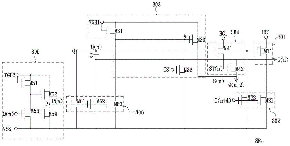
图3B是本发明的移位暂存器电路实施例二示意图。FIG. 3B is a schematic diagram of the second embodiment of the shift register circuit of the present invention.
图4A是本发明的低温状态信号时序实施例示意图。FIG. 4A is a schematic diagram of an embodiment of a low temperature state signal timing sequence according to the present invention.
图4B是本发明的常温状态信号时序实施例示意图。FIG. 4B is a schematic diagram of an embodiment of a normal temperature state signal timing sequence according to the present invention.
图5是本发明的移位暂存器电路操作方法实施例示意图。FIG. 5 is a schematic diagram of an embodiment of a method for operating a shift register circuit of the present invention.
图6是本发明的上拉控制信号模拟实施例示意图。FIG. 6 is a schematic diagram of a simulation embodiment of a pull-up control signal according to the present invention.
其中,附图标记:Among them, reference numerals:
100:显示器 110:面板100: Display 110: Panel
120:时序控制电路 130:栅极驱动器120: Timing Control Circuit 130: Gate Driver
140:数据驱动器 HC1~HC8:时脉信号140: Data driver HC1~HC8: Clock signal
G1、G2、G3……Gn:栅极线 D1、D2…Dm:资料线G 1 , G 2 , G 3 , ... G n : gate lines D 1 , D 2 , ... D m : data lines
SR、SRn、SRn+1、SRn+2、SRn+3、SRn+4、SRn+5、SRn+6、SRn+7:移位暂存器电路SR, SRn , SRn +1 , SRn +2 , SRn +3 , SRn +4 , SRn +5 , SRn +6 , SRn +7 : Shift register circuit
A、P、Q:节点A, P, Q: Nodes
G(1)、G(2)、G(3)、G(n-2)、G(n)、G(n+1)、G(n+2)、G(n+3)、G(n+4)、G(n+5)、G(n+6)、G(n+7):栅极驱动信号G(1), G(2), G(3), G(n-2), G(n), G(n+1), G(n+2), G(n+3), G( n+4), G(n+5), G(n+6), G(n+7): gate drive signal
Q(n-2)、Q(n)、Q(n+1)、Q(n+2)、Q(n+3)、Q(n+4)、Q(n+5)、Q(n+6)、Q(n+7)、Q(n+8)、Q(n+9):上拉控制信号Q(n-2), Q(n), Q(n+1), Q(n+2), Q(n+3), Q(n+4), Q(n+5), Q(n +6), Q(n+7), Q(n+8), Q(n+9): pull-up control signal
ST(n-2)、ST(n):起始控制信号 S(n):补偿信号ST(n-2), ST(n): start control signal S(n): compensation signal
CS:控制信号 CSd:前级信号CS: Control signal CS d : Pre-stage signal
P(n):下拉控制信号 301:上拉电路P(n): Pull-down control signal 301: Pull-up circuit
302:主下拉电路 303:补偿电路302: Main pull-down circuit 303: Compensation circuit
304:上拉控制电路 305:下拉控制电路304: Pull-up control circuit 305: Pull-down control circuit
306:第一下拉电路 307:第二下拉电路306: The first pull-down circuit 307: The second pull-down circuit
601:补偿的上拉控制信号 602:未补偿的上拉控制信号601: Compensated pull-up control signal 602: Uncompensated pull-up control signal
C:电容C: Capacitor
M11、M21、M22、M31、M32、M33、M41、M42、M51、M52、M53、M54、M61、M62、M63、M71:晶体管M11, M21, M22, M31, M32, M33, M41, M42, M51, M52, M53, M54, M61, M62, M63, M71: Transistors
VSS、VGH1、VGH2:电压准位VSS, VGH1, VGH2: Voltage levels
V1、V1’:第一阶段电压准位V 1 , V 1 ': the voltage level of the first stage
V2、V2’:第二阶段电压准位V 2 , V 2 ': the voltage level of the second stage
V3、V3’:第三阶段电压准位V 3 , V 3 ': the voltage level of the third stage
V4’:第四阶段电压准位V 4 ': the fourth stage voltage level
具体实施方式Detailed ways
请参考图1,图1为显示器实施例示意图,显示器例如为液晶显示装置,但不以此为限。在此实施例中,显示器100包括面板110、时序控制电路120、栅极驱动器130以及数据驱动器140。时序控制电路120与栅极驱动器130电性连接,时序控制电路120是用以输出多个时脉信号HC1~HC8至栅极驱动器130。栅极驱动器130与多条栅极线G1、G2、G3…Gn电性连接,栅极驱动器130是用以输出多级的栅极驱动信号G(1)、G(2)、G(3)…G(n)至对应的栅极线,其中n为大于零的正整数。数据驱动器140与多条资料线D1、D2…Dm电性连接,数据驱动器140是用以输出多个显示资料至电性连接的多条资料线D1、D2…Dm,其中m为大于零的正整数。面板110包括多个像素111,每一个像素111个别的与多条栅极线G1、G2、G3…Gn以及多条资料线D1、D2…Dm的其中之一电性连接,像素111是用以根据接收的栅极驱动信号决定是否接收显示资料。Please refer to FIG. 1 . FIG. 1 is a schematic diagram of an embodiment of a display. The display is, for example, a liquid crystal display device, but not limited thereto. In this embodiment, the
请参考图2,图2为本发明的栅极驱动器130实施例一示意图,栅极驱动器130包括多级的移位暂存器电路SR,图2以栅极驱动器130至少包括第n级移位暂存器电路SRn、第n+1级移位暂存器电路SRn+1、第n+2级移位暂存器电路SRn+2、第n+3级移位暂存器电路SRn+3、第n+4级移位暂存器电路SRn+4、第n+5级移位暂存器电路SRn+5、第n+6级移位暂存器电路SRn+6以及第n+7级移位暂存器电路SRn+7为例,但不以此为限。第n级移位暂存器电路SRn用以接收时脉信号HC1以及第n-2级移位暂存器电路SRn-2(未绘示)输出的第n级上拉控制信号Q(n),第n级移位暂存器电路SRn并用以输出第n级栅极驱动信号G(n)。第n+1级移位暂存器电路SRn+1用以接收时脉信号HC2以及第n-1级移位暂存器电路SRn-1(未绘示)输出的第n+1级上拉控制信号Q(n+1),第n+1移位暂存器电路SRn+1并用以输出第n+1栅极驱动信号G(n+1)。第n+2级移位暂存器电路SRn+2用以接收时脉信号HC3以及第n级移位暂存器电路SRn输出的第n+2级上拉控制信号Q(n+2),第n+2级移位暂存器电路SRn+2并用以输出第n+2级栅极驱动信号G(n+2)。第n+3级移位暂存器电路SRn+3用以接收时脉信号HC4以及第n+1级移位暂存器电路SRn+1输出的第n+3级上拉控制信号Q(n+3),第n+3级移位暂存器电路SRn+3并用以输出第n+3级栅极驱动信号G(n+3)。第n+4级移位暂存器电路SRn+4用以接收时脉信号HC5以及第n+2级移位暂存器电路SRn+2输出的第n+4级上拉控制信号Q(n+4),第n+4级移位暂存器电路SRn+4并用以输出第n+4级栅极驱动信号G(n+4)。第n+5级移位暂存器电路SRn+5用以接收时脉信号HC6以及第n+3级移位暂存器电路SRn+3输出的第n+5级上拉控制信号Q(n+5),第n+5级移位暂存器电路SRn+5并用以输出第n+5级栅极驱动信号G(n+5)。第n+6级移位暂存器电路SRn+6用以接收时脉信号HC7以及第n+4级移位暂存器电路SRn+4输出的第n+6级上拉控制信号Q(n+6),第n+6级移位暂存器电路SRn+6并用以输出第n+8级上拉控制信号Q(n+8)以及第n+6级栅极驱动信号G(n+6)。第n+7级移位暂存器电路SRn+7用以接收时脉信号HC8以及第n+5级移位暂存器电路SRn+5输出的第n+7级上拉控制信号Q(n+7),第n+7级移位暂存器电路SRn+7并用以输出第n+9级上拉控制信号Q(n+9)以及第n+7级栅极驱动信号G(n+7)。Please refer to FIG. 2 . FIG. 2 is a schematic diagram of a
请参考图3A,图3A为本发明的移位暂存器电路SR实施例示意图,图3A更以输出第n级栅极驱动信号G(n)的第n级移位暂存器电路SRn为例来说明。移位暂存器电路SRn包括节点Q、上拉电路301、主下拉电路302、补偿电路303、上拉控制电路304、下拉控制电路305以及第一下拉电路306。节点Q是用以接收前级移位暂存器电路SR输出的信号,例如为第n-2级移位暂存器电路SRn-2输出的第n-2级起始控制信号ST(n-2),但不以此为限,节点Q并根据接收的第n-2级起始控制信号ST(n-2)产生第n级上拉控制信号Q(n)。Please refer to FIG. 3A . FIG. 3A is a schematic diagram of an embodiment of the shift register circuit SR of the present invention, and FIG. 3A further illustrates the n-th stage shift register circuit SR n that outputs the n-th stage gate driving signal G(n). Example to illustrate. The shift register circuit SR n includes a node Q, a pull-up
所述上拉电路301包括晶体管M11,晶体管M11具有第一端、控制端以及第二端,晶体管M11的第一端用以接收时脉信号HC1,晶体管M11的控制端与节点Q电性连接并接收第n级上拉控制信号Q(n),晶体管M11的第二端用以输出第n级栅极驱动信号G(n),其中,晶体管M11的第二端以及控制端之间并透过电容C彼此电性连接。The pull-up
所述主下拉电路302与上拉电路301电性连接,主下拉电路302是用以将第n级栅极驱动信号G(n)与上拉控制信号Q(n)维持于禁能电压准位。主下拉电路302包括晶体管M21以及晶体管M22。晶体管M21具有第一端、控制端以及第二端,晶体管M21的第一端与晶体管M11的第二端电性连接,晶体管M21的第一端是用以接收第n级栅极驱动信号G(n),晶体管M21的控制端用以接收第n+4级移位暂存器电路SRn+4所输出的第n+4级栅极控制信号G(n+4),晶体管M21的第二端用以接收电压准位VSS,在此实施例中,电压准位VSS例如为逻辑低电位。晶体管M22具有第一端、控制端以及第二端,晶体管M22的第一端与节点Q电性连接并接收第n级上拉控制信号Q(n),晶体管M22的控制端用以接收第n+4级栅极控制信号G(n+4),晶体管M22的第二端用以接收电压准位VSS。因此,在此实施例中,当晶体管M21以及晶体管M22因为第n+4级栅极控制信号G(n+4)被致能时,第n级上拉控制信号Q(n)以及第n级栅极驱动信号G(n)会因此转换为禁能电压准位。The main pull-
所述补偿电路303是用以根据节点A的电压决定是否输出补偿信号S(n)。补偿电路303包括晶体管M31、晶体管M32以及晶体管M33。晶体管M31具有第一端、控制端以及第二端,晶体管M31的第一端与控制端彼此电性连接并用以接收电压准位VGH1,晶体管M31的第二端与节点A电性连接。晶体管M32具有第一端、控制端以及第二端,晶体管M32的第一端与节点A电性连接,晶体管M32的控制端接收控制信号CS,晶体管M32的第二端用以接收电压准位VSS,其中,控制信号CS在不同实施例中可以为第n级上拉控制信号Q(n)或第n-2级上拉控制信号Q(n-2)等可直接体现当级晶体管元件驱动能力的信号。晶体管M33具有第一端、控制端以及第二端,晶体管M33的第一端与晶体管M31的第一端以及控制端电性连接,晶体管M33的第一端用以接收电压准位VGH1,晶体管M33的控制端为所述节点A,晶体管M33的第二端用以输出补偿信号S(n)。其中,电压准位VGH1是用以产生对应的补偿信号S(n),因此电压准位VGH1可根据需求的补偿信号S(n)来调整其电压值大小,例如为逻辑高电位,但不以此为限。The
由于补偿电路303的晶体管M32是根据控制信号CS来决定晶体管M32的驱动能力,因此当第n级移位暂存器电路SRn操作时的环境温度为常温状态,例如当前环境温度等于或高于温度阈值(例如为25℃),此时补偿电路303因为当前温度而操作于驱动模式,晶体管控制信号CS为具有正常驱动能力的电压准位,晶体管M32可产生相对较大的导通电流,因此晶体管M32等效的电阻值较小,故晶体管M31与晶体管M32的分压导致节点A上的电压相对较小并小于晶体管M33的致能电压准位,晶体管M33因为节点A的电压而禁能,第n级补偿信号S(n)为禁能电压准位。反之,当环境温度为低温状态,也就是当前环境温度低于温度阈值,补偿电路303操作于补偿模式,晶体管M32因为温度影响而具有相对较低的导通电流,控制信号CS为相对较低的电压准位,晶体管M32等效的电阻值较大,晶体管M31与晶体管M32的分压导致节点A上的电压相对较大并等于或大于晶体管M33的致能电压准位,晶体管M33因此致能,第n级补偿信号S(n)转换对第n+2级上拉控制信号Q(n+2)进行补偿。Since the transistor M32 of the
所述上拉控制电路304与补偿电路303电性连接,上拉控制电路304用以根据第n级起始控制信号ST(n)以及第n级补偿信号S(n)输出第n+2级上拉控制信号Q(n+2)至一后级移位暂存器电路SR,在本实施例中,后级移位暂存器电路SR为第n+2级移位暂存器电路SRn+2。因此,在低温状态时,第n+2级移位暂存器电路SRn+2可通过第n级起始控制信号ST(n)以及第n级补偿信号S(n)产生第n+2级上拉控制信号Q(n+2)。The pull-up
上拉控制电路304包括晶体管M41以及晶体管M42,晶体管M41具有第一端、控制端以及第二端,晶体管M41的第一端用以接收时脉信号HC1,晶体管M41的控制端用以接收第n级上拉控制信号Q(n),晶体管M41的第二端用以输出第n级起始控制信号ST(n)。晶体管M42的第一端与晶体管M11的第二端电性连接并用以接收第n级栅极驱动信号G(n),晶体管M42的控制端与晶体管M41的第二端电性连接,晶体管M42的第二端与晶体管M33的第二端电性连接并接收补偿信号S(n),晶体管M42的第二端用以输出第n+2级上拉控制信号Q(n+2)。The pull-up
所述下拉控制电路305是用以接收第n级上拉控制信号Q(n)并输出第n级下拉控制信号P(n)。下拉控制电路305包括晶体管M51、晶体管M52、晶体管M53以及晶体管M54。晶体管M51具有第一端、控制端以及第二端,晶体管M51的第一端以及控制端彼此电性连接并用以接收电压准位VGH2,电压准位VGH2例如为逻辑高电位,但不以此为限。晶体管M52具有第一端、控制端以及第二端,晶体管M52的第一端与晶体管M51的第一端以及控制端电性连接并接收电压准位VGH2,晶体管M52的控制端与晶体管M51的第二端电性连接,晶体管M52的第二端与节点P电性连接,节点P用以形成第n级下拉控制信号P(n)。晶体管M53具有第一端、控制端以及第二端,晶体管M53的第一端与晶体管M51的第二端以及晶体管M52的控制端电性连接,晶体管M53的控制端用以接收第n级上拉控制信号Q(n),晶体管M53的第二端用以接收电压准位VSS。晶体管M54具有第一端、控制端以及第二端,晶体管M54的第一端与节点P电性连接并接收第n级下拉控制信号P(n),晶体管M54的控制端用以接收第n级上拉控制信号Q(n),晶体管M54的第二端用以接收电压准位VSS。The pull-
所述第一下拉电路306用以根据第n级下拉控制信号P(n)决定是否将第n级上拉控制信号Q(n)、第n级栅极驱动信号G(n)以及节点A稳定于禁能电压准位。第一下拉电路306包括晶体管M61、晶体管M62以及晶体管M63。晶体管M61具有第一端、控制端以及第二端,晶体管M61的第一端与节点Q电性连接并用以接收第n级上拉控制信号Q(n),晶体管M61的控制端用以接收第n级下拉控制信号P(n),晶体管M61的第二端用以接收电压准位VSS。晶体管M62具有第一端、控制端以及第二端,晶体管M62的第一端用以接收第n级栅极驱动信号G(n),晶体管M62的控制端用以接收第n级下拉控制信号P(n),晶体管M62的第二端用以接收电压准位VSS。晶体管M63具有第一端、控制端以及第二端,晶体管M63的第一端用以与节点A电性连接,晶体管M63的控制端用以接收第n级下拉控制信号P(n),晶体管M63的第二端用以接收电压准位VSS。The first pull-
请参考图3B,图3B为移位暂存器电路SR实施例二示意图,图3B与图3A的差别在于,图3B的移位暂存器电路SRn更包括了第二下拉电路307,第二下拉电路307与节点A电性连接并用以根据前级信号CSd决定是否将节点A稳定于禁能电压准位。在一实施例中,当前级信号CSd为第n-2级栅极驱动信号G(n-2),控制信号CS为第n级栅极驱动信号G(n)。在另一实施例中,当前级信号CSd为第n-2级起始控制信号ST(n-2),控制信号CS为第n级起始控制信号ST(n)但不以此为限。在此实施例中,第二下拉电路307包括晶体管M71,晶体管M71的第一端与节点A电性连接,晶体管M71的控制端接收上述前级信号CSd,晶体管M71的第二端与电压准位VSS电性连接。Please refer to FIG. 3B . FIG. 3B is a schematic diagram of the second embodiment of the shift register circuit SR. The difference between FIG. 3B and FIG. 3A is that the shift register circuit SR n of FIG. 3B further includes a second pull-
以下接着配合图3A以及图4A说明移位暂存器电路SR的操作方法,图4A为移位暂存器电路SR操作于低温状态的信号实施例示意图。在此实施例中,并以控制信号CS为第n级上拉控制信号Q(n)为例进行说明。首先,于时段T1,第n级上拉控制信号Q(n)的电压因为第n-2级起始控制信号ST(n-2)而由禁能电压准位转换为第一阶段电压准位V1。下拉控制电路305的晶体管M53以及晶体管M54因为第n级上拉控制信号Q(n)而致能,节点P的电压准位被稳定于禁能电压准位,第n级下拉控制信号P(n)因而由致能电压准位转换为禁能电压准位。第一下拉电路306的晶体管M61、晶体管M62以及晶体管M63因此为禁能。补偿电路303的节点A的电压因为第n级上拉控制信号Q(n)提升为晶体管M33的致能电压准位,晶体管M33为开启,第n级补偿信号S(n)因此为补偿电压准位。上拉控制电路304因为第n级上拉控制信号Q(n)而致能,然第n级栅极驱动信号G(n)于现在时点仍为禁能电压准位,因此第n+2级上拉控制信号Q(n+2)因为补偿信号S(n)为第一阶段电压准位V1’。Next, an operation method of the shift register circuit SR will be described with reference to FIG. 3A and FIG. 4A . FIG. 4A is a schematic diagram of a signal embodiment of the shift register circuit SR operating in a low temperature state. In this embodiment, the control signal CS is taken as an example of the n-th pull-up control signal Q(n) for description. First, in the period T1, the voltage of the n-th stage pull-up control signal Q(n) is converted from the disabled voltage level to the first-stage voltage level due to the n-2 stage start control signal ST(n-2). V1 . The transistor M53 and the transistor M54 of the pull-
于时段T2,第n-2级起始控制信号ST(n-2)由致能电压准位转换为禁能电压准位,第n级上拉控制信号Q(n)先因为节点Q为浮接(floating)而保持在第一阶段电压准位V1。上拉电路301因为上拉控制信号Q(n)而保持开启,时脉信号HC1在时段T2由禁能电压准位转换为致能电压准位,因此第n级栅极驱动信号G(n)由禁能电压准位转换为致能电压准位,第n级栅极驱动信号G(n)并通过电容C使第n级上拉控制信号Q(n)提升至第二阶段电压准位V2。第n级下拉控制信号P(n)因为第n级上拉控制信号Q(n)维持于禁能电压准位,补偿电路303的节点A保持于致能电压准位,第n级补偿信号S(n)持续对第n+2级上拉控制信号Q(n+2)进行补偿。因此第n+2级上拉控制信号Q(n+2)转换为第二阶段电压准位V2’。In the period T2, the start control signal ST(n-2) of the n-2 stage is converted from the enable voltage level to the disable voltage level, and the n-th stage pull-up control signal Q(n) is first because the node Q is floating. It is floating and kept at the first-stage voltage level V 1 . The pull-up
于时段T3,第n级栅极驱动信号G(n)因为时脉信号HC1而由致能电压准位转换为禁能电压准位,第n级上拉控制信号Q(n)因此由第二阶段电压准位V2转换为第三阶段电压准位V3,第n级下拉控制信号P(n)因为第n级上拉控制信号Q(n)而维持于禁能电压准位,补偿电路303的节点A保持致能电压准位,但由于第n+2级上拉控制信号Q(n+2)因第n+2级栅极驱动信号G(n+2)通过电容C使第n+2级上拉控制信号Q(n+2)提升至第二阶段电压准位V3’,并且V3’电压准位高于节点A的致能电压准位,因此晶体管M33转变为禁能状态,补偿信号S(n)结束对第n+2级上拉控制信号Q(n+2)进行补偿。In the period T3, the gate driving signal G(n) of the nth stage is converted from the enable voltage level to the disable voltage level due to the clock signal HC1, and the pull-up control signal Q(n) of the nth stage is thus changed by the second level. The stage voltage level V 2 is converted to the third stage voltage level V 3 , the nth stage pull-down control signal P(n) is maintained at the disabled voltage level due to the nth stage pull-up control signal Q(n), the
于时段T4,用以产生栅极驱动信号G(n+4)的时脉信号HC5为致能电压准位,晶体管M21以及晶体管M22因为栅极驱动信号G(n+4)而开启,第n级上拉控制信号Q(n)因此转换为禁能电压准位,第n级下拉控制信号P(n)因为晶体管M53以及晶体管M54被禁能而转换为致能电压准位,晶体管M61、晶体管M62以及晶体管M63因此致能,第n级上拉控制信号Q(n)、第n级栅极驱动信号G(n)以及节点A被稳定于禁能电压准位,第n+2级上拉控制信号Q(n+2)转换为第四阶段电压准位V4’。During the period T4, the clock signal HC5 for generating the gate driving signal G(n+4) is at the enabling voltage level, the transistor M21 and the transistor M22 are turned on due to the gate driving signal G(n+4), and the nth The stage pull-up control signal Q(n) is thus converted to a disable voltage level, and the nth stage pull-down control signal P(n) is converted to an enable voltage level because the transistor M53 and the transistor M54 are disabled, the transistor M61, the transistor M54 M62 and transistor M63 are thus enabled, the n-th stage pull-up control signal Q(n), the n-th stage gate driving signal G(n) and node A are stabilized at the disabled voltage level, and the n+2-th stage pull-up control The signal Q(n+2) is converted into the fourth-stage voltage level V 4 ′.
在此实施例中,补偿信号S(n)于时段T1-T2期间持续的对第n+2级上拉控制信号Q(n+2)进行补偿,因此使第n+2级上拉控制信号Q(n+2)可维持于一个相对较高的电压准位,移位暂存器电路因而可在低温状态下正常运作。In this embodiment, the compensation signal S(n) continuously compensates the n+2-th stage pull-up control signal Q(n+2) during the period T1-T2, thus making the n+2-th stage pull-up control signal Q(n+2) can be maintained at a relatively high voltage level, so that the shift register circuit can operate normally in a low temperature state.
接着请参考图4B,在此实施例中,移位暂存器电路SR操作于常温状态。因此在此实施例中,于时段T1到T3,第n级上拉控制信号Q(n)保有足够的驱动能力来驱动晶体管,第n级上拉控制信号Q(n)不需进行补偿,晶体管M32因为上拉控制信号Q(n)而具有较小的等效电阻,节点A的电压因此较低温状态时来的低,晶体管M33保持关闭,补偿信号S(n)因此保持为禁能电压准位,在此实施例中补偿信号S(n)不需对上拉控制信号Q(n)进行补偿。Next, please refer to FIG. 4B , in this embodiment, the shift register circuit SR operates in a normal temperature state. Therefore, in this embodiment, during the period T1 to T3, the n-th stage pull-up control signal Q(n) retains enough driving capability to drive the transistor, and the n-th stage pull-up control signal Q(n) does not need to be compensated, and the transistor M32 has a smaller equivalent resistance due to the pull-up control signal Q(n), the voltage of node A is therefore lower when the temperature is lower, the transistor M33 is kept off, and the compensation signal S(n) is therefore kept at the disable voltage level In this embodiment, the compensation signal S(n) does not need to compensate the pull-up control signal Q(n).
根据上述内容,本发明还可汇集整理出移位暂存器电路SR的操作方法实施例。请参考图5,于步骤501,移位暂存器电路SR判断环境温度是否低于温度阈值。进一步的说,当上述节点A的电压小于致能电压准位,即可判断环境温度高于温度阈值,反之当节点A的电压大于或等于致能电压准位,可判断环境温度低于温度阈值。当步骤501判断为是,进行步骤502,补偿电路303操作于补偿模式,晶体管M33为致能,补偿信号S(n)对第n+2级上拉控制信号Q(n+2)进行补偿。反之,执行步骤503,补偿电路303操作于驱动模式,晶体管M33为禁能,补偿信号S(n)不对第n+2级上拉控制信号Q(n+2)进行补偿。执行完步骤502或步骤503后,移位暂存器电路SR结束流程并等待下一次被致能。According to the above-mentioned content, the present invention can also collect and sort out the embodiments of the operation method of the shift register circuit SR. Referring to FIG. 5 , in
请参考图6,图6为本发明的上拉控制信号于低温状态的模拟实施例示意图。图6中X轴为时间,Y轴为电压,符号601为通过本发明的补偿信号进行补偿的上拉控制信号,符号602为未进行补偿的上拉控制信号,由图6中明显可以看出,补偿过后的上拉控制信号601具有相对较高的电压值,明显具有较佳的驱动能力。Please refer to FIG. 6 . FIG. 6 is a schematic diagram of a simulated embodiment of the pull-up control signal of the present invention in a low temperature state. In FIG. 6 , the X axis is time, the Y axis is voltage, the
综上所述,由于本发明的补偿电路303可根据环境温度决定是否通过补偿信号来对后级移位暂存器电路的上拉控制信号进行补偿,因此可有效提升上拉控制信号于低温状态的驱动能力,使移位暂存器电路于低温状态时仍可稳定的正常操作,增进移位暂存器电路整体的驱动能力。To sum up, since the
Claims (14)
Applications Claiming Priority (2)
| Application Number | Priority Date | Filing Date | Title |
|---|---|---|---|
| TW106133965 | 2017-09-30 | ||
| TW106133965A TWI631568B (en) | 2017-09-30 | 2017-09-30 | Shift register circuit and operation method thereof |
Publications (2)
| Publication Number | Publication Date |
|---|---|
| CN107680552A CN107680552A (en) | 2018-02-09 |
| CN107680552B true CN107680552B (en) | 2020-08-04 |
Family
ID=61148858
Family Applications (1)
| Application Number | Title | Priority Date | Filing Date |
|---|---|---|---|
| CN201711120065.XA Active CN107680552B (en) | 2017-09-30 | 2017-11-14 | Shift register circuit and method of operation thereof |
Country Status (2)
| Country | Link |
|---|---|
| CN (1) | CN107680552B (en) |
| TW (1) | TWI631568B (en) |
Families Citing this family (2)
| Publication number | Priority date | Publication date | Assignee | Title |
|---|---|---|---|---|
| TWI728698B (en) * | 2020-02-14 | 2021-05-21 | 友達光電股份有限公司 | Lcd driving circuit |
| US11171584B1 (en) * | 2020-05-11 | 2021-11-09 | Pix Art Imaging Inc. | Interpolation circuit and motor driving circuit |
Citations (3)
| Publication number | Priority date | Publication date | Assignee | Title |
|---|---|---|---|---|
| CN102426817A (en) * | 2011-06-29 | 2012-04-25 | 友达光电股份有限公司 | Shift register circuit |
| CN102982846A (en) * | 2012-07-18 | 2013-03-20 | 友达光电股份有限公司 | Shift register for light-induced touch panel |
| CN105630242A (en) * | 2015-11-06 | 2016-06-01 | 友达光电股份有限公司 | shift register circuit |
Family Cites Families (8)
| Publication number | Priority date | Publication date | Assignee | Title |
|---|---|---|---|---|
| TWI298478B (en) * | 2002-06-15 | 2008-07-01 | Samsung Electronics Co Ltd | Method of driving a shift register, a shift register, a liquid crystal display device having the shift register |
| KR100917009B1 (en) * | 2003-02-10 | 2009-09-10 | 삼성전자주식회사 | Transistor driving method and shift register driving method and shift register for performing the same |
| JP3870954B2 (en) * | 2003-07-31 | 2007-01-24 | セイコーエプソン株式会社 | Liquid crystal panel driving method, liquid crystal device and electronic apparatus |
| US20100188385A1 (en) * | 2007-07-24 | 2010-07-29 | Koninklijke Philips Electronics N.V. | Shift register circuit having threshold voltage compensation |
| TWI426526B (en) * | 2009-08-12 | 2014-02-11 | Au Optronics Corp | Shift register circuit |
| TWI563514B (en) * | 2015-06-05 | 2016-12-21 | Au Optronics Corp | Shift register circuit |
| TWI578297B (en) * | 2016-07-06 | 2017-04-11 | 友達光電股份有限公司 | Shift register |
| CN106448606A (en) * | 2016-11-23 | 2017-02-22 | 深圳市华星光电技术有限公司 | GOA (gate driver on array) driving circuit |
-
2017
- 2017-09-30 TW TW106133965A patent/TWI631568B/en active
- 2017-11-14 CN CN201711120065.XA patent/CN107680552B/en active Active
Patent Citations (3)
| Publication number | Priority date | Publication date | Assignee | Title |
|---|---|---|---|---|
| CN102426817A (en) * | 2011-06-29 | 2012-04-25 | 友达光电股份有限公司 | Shift register circuit |
| CN102982846A (en) * | 2012-07-18 | 2013-03-20 | 友达光电股份有限公司 | Shift register for light-induced touch panel |
| CN105630242A (en) * | 2015-11-06 | 2016-06-01 | 友达光电股份有限公司 | shift register circuit |
Also Published As
| Publication number | Publication date |
|---|---|
| TW201916057A (en) | 2019-04-16 |
| TWI631568B (en) | 2018-08-01 |
| CN107680552A (en) | 2018-02-09 |
Similar Documents
| Publication | Publication Date | Title |
|---|---|---|
| JP5128102B2 (en) | Shift register circuit and image display apparatus including the same | |
| KR102383363B1 (en) | Gate driver and display device having the same | |
| KR102448227B1 (en) | Gate driving circuit and display device including same | |
| JP4990034B2 (en) | Shift register circuit and image display apparatus including the same | |
| CN104167166B (en) | Shift register and method for driving shift register | |
| CN104992662B (en) | GOA unit and its driving method, GOA circuits, display device | |
| US8248353B2 (en) | Method and device for reducing voltage stress at bootstrap point in electronic circuits | |
| CN106782280B (en) | Shift register and grid drive circuit | |
| TWI718867B (en) | Gate driving circuit | |
| CN103956133B (en) | shift register circuit and shift register | |
| JP2007317288A (en) | Shift register circuit and image display apparatus including the same | |
| TW201539420A (en) | Gate driving circuit and shift register | |
| TWI426521B (en) | Bidirectional shift register | |
| CN105493195A (en) | Shift register and display device | |
| KR20160089909A (en) | Driver and display device having the same | |
| CN108510938B (en) | Shift register and driving method thereof, emission driving circuit and display device | |
| CN107731170A (en) | Compensating module, drive element of the grid, circuit and its driving method and display device | |
| CN106940987A (en) | Driver and driving method thereof | |
| CN109427275B (en) | Shift register unit, gate driving circuit and driving method | |
| TW202034339A (en) | Shift register circuit and gate driving circuit | |
| CN105632451A (en) | Shifting register unit, driving method, gate drive circuit and display device | |
| WO2019134413A1 (en) | Shift register unit, gate drive circuit, display device, and control method therefor | |
| WO2017185822A1 (en) | Shift register, gate driver circuit, array substrate | |
| CN107093399A (en) | shift register circuit | |
| CN100565711C (en) | Shift register circuit and image display device provided with the same |
Legal Events
| Date | Code | Title | Description |
|---|---|---|---|
| PB01 | Publication | ||
| PB01 | Publication | ||
| SE01 | Entry into force of request for substantive examination | ||
| SE01 | Entry into force of request for substantive examination | ||
| GR01 | Patent grant | ||
| GR01 | Patent grant |