JP3843658B2 - Electro-optical device drive circuit, electro-optical device, and electronic apparatus - Google Patents
Electro-optical device drive circuit, electro-optical device, and electronic apparatus Download PDFInfo
- Publication number
- JP3843658B2 JP3843658B2 JP26853299A JP26853299A JP3843658B2 JP 3843658 B2 JP3843658 B2 JP 3843658B2 JP 26853299 A JP26853299 A JP 26853299A JP 26853299 A JP26853299 A JP 26853299A JP 3843658 B2 JP3843658 B2 JP 3843658B2
- Authority
- JP
- Japan
- Prior art keywords
- sampling
- circuit
- electro
- shift register
- optical device
- Prior art date
- Legal status (The legal status is an assumption and is not a legal conclusion. Google has not performed a legal analysis and makes no representation as to the accuracy of the status listed.)
- Expired - Fee Related
Links
Images


Landscapes
- Devices For Indicating Variable Information By Combining Individual Elements (AREA)
- Liquid Crystal (AREA)
- Shift Register Type Memory (AREA)
- Liquid Crystal Display Device Control (AREA)
- Control Of Indicators Other Than Cathode Ray Tubes (AREA)
Description
【0001】
【発明の属する技術分野】
本発明は、薄膜トランジスタ(以下適宜、TFTと称す)駆動、薄膜ダイオード(以下適宜、TFDと称す)駆動等によるアクティブマトリクス駆動方式などの電気光学装置(例えば、液晶装置等)の駆動回路及び該駆動回路を内蔵する電気光学装置の技術分野に属し、特に、プロジェクタのライトバルブ等として好適に用いられる電気光学装置の駆動回路の技術分野に属する。
【0002】
【従来の技術】
従来、この種のプロジェクタのライトバルブとして液晶装置等の電気光学装置を用いる場合には、対向基板にカラーフィルタが形成された電気光学装置を1枚だけ用いる単板方式と、カラーフィルタが形成されていない電気光学装置をRGB別に3枚用いる複板方式とがある。単板方式は、構成が簡易であるが、表示画面を明るくして高品位の画質が得られる点で複板方式は、より優れている。この複板方式によれば、3枚の電気光学装置により別々に光変調された3色光は、プリズムやダイクロイックミラーにより一つの投射光に合成された後、スクリーン上に投射される。
【0003】
このように、プリズム等で合成すると、例えば、図13に示したように、RGB用の3枚のライトバルブ500R、500G及び、500Bによる変調後にプリズム502で反射するR光及びB光と比べると、G光は、プリズム502で反射されない。即ち、光の反転回数が一回だけG光について少なくなる。この現象は、もちろんG光の代わりに、R光又はB光がプリズムで反射されないように光学系を構成しても同じであり、更に、ダイクロイックミラー等用いて3色光を合成した場合にも同様に起こる。従って、このような場合、G光についての画像信号を何等かの形で左右に反転する必要性が生じる。
【0004】
他方、商品戦略上、単板方式や複板方式のプロジェクタを、床に普通に設置する床置きタイプとしても、天井に逆さに取り付けて設置する天吊りタイプとしても使用可能に構成したい場合がある。この場合、単板方式においても、設置の仕方に応じて電気光学装置に供給される画像信号を上下左右に反転する必要性が生じる。また、携帯型ビデオカメラの液晶モニタのように、単板方式の電気光学装置である液晶モニタを、ユーザの撮影姿勢に応じて、例えばフレキシブルジョイントを支点に反転して見れるようにしたい場合もある。この場合やはり、電気光学装置に供給される画像信号を何等かの形で上下左右に反転する必要性が生じる。
【0005】
そこで従来は、電気光学装置におけるデータ線駆動回路に画像信号を所定フォーマットで供給する画像信号処理用ICで、例えばG用の画像信号についてだけ、或いは全ての色用の画像信号について、原画像に対して上下左右が反転した画像に対応する画像信号を1フィールド毎に生成して供給する。このようにすれば、特に電気光学装置や駆動回路に何等の変更を施す必要はないので便利である。
【0006】
或いは従来は、例えば前述のように3色光を合成するためには、R用の電気光学装置及びB用の電気光学装置と比較して、走査方向が左右に反転した電気光学装置が、G用の電気光学装置として用いられている。
【0007】
【発明が解決しようとする課題】
しかしながら、前述した従来の画像信号処理用ICを用いて画像信号を上下左右に反転する方式は、近時の高品位画像に対応するためには、画像信号処理用ICにかかる負担が大き過ぎて実践的ではなくなってしまう。
【0008】
また、走査方向が上下左右に反転したG用の電気光学装置を用いる方式には以下の問題点がある。即ち、一般に走査線駆動回路やデータ線駆動回路は、転送方向が一方に固定された単一方向シフトレジスタを有し、該単一方向シフトレジスタから発生される転送信号に基づいて、線順次や点順次などで走査信号や画像信号を供給して、上下左右に表示画面上で走査するように構成されている。従って、走査方向が反転したG用の電気光学装置を用いるためには、データ線駆動回路が表示画面に対して左から右へ走査するようにシフトレジスタが構成されたRシフト型電気光学装置と、データ線駆動回路が表示画面に対して右から左へ走査するようにシフトレジスタが構成されたLシフト型電気光学装置との2種類を製造する必要性が生じる。このように2種類の電気光学装置を、例えば半導体製造装置等によるTFTの製造工程等で製造するのは、製造者の立場からして明らかに不利である。また、使用者の立場からしても、似たような電気光学装置間で互換性がなく、個々の装置はどれも、いずれかのタイプとしてしか使用できないという実用上の問題点がある。更に、このように走査方向が固定された電気光学装置では、前述した床置きタイプとしても天吊りタイプとしても使用可能なプロジェクタや、画面が上下左右に反転する携帯型ビデオカメラの液晶モニタを実現できない。
【0009】
また仮に走査線駆動回路やデータ線駆動回路に双方向シフトレジスタを採用して、出力される転送信号の転送方向を上下や左右に反転させる構成とすれば、走査信号や画像信号の供給順序を反転させること、即ち水平走査方向や垂直走査方向を上下左右に反転することが可能である。しかしながら、仮に双方向シフトレジスタを採用した場合には、前述の単一方向シフトレジスタの場合と比較して、シフトレジスタを構成するゲート数が多くなるので、全体におけるゲート容量の増加分だけ、消費電力が増加してしまうという問題点がある。
【0010】
更に、仮に双方向シフトレジスタを採用した場合には、特にシリアル−パラレル変換された画像信号による表示を行う際に、画像信号による水平走査方向を反転させるのに合わせて、複数の画像信号線に対してパラレルに供給する画像信号の順番も入れ換える必要が生じるという問題点がある。
【0011】
より具体的には、例えば図14の上半分に示すように、シリアル−パラレル変換された画像信号VID1〜VID6を供給する場合を考える。この場合、外部の画像信号処理用ICにより、時間ΔTの間に表示画像一フィールド分の画素データ#1〜#6n(但し、nは自然数)が、画像信号VID1〜VID6に順次割り当てられて6本の画像信号線No.1〜No.6に供給される。図14の上半分に図示したように、通常の水平走査を6本同時駆動又は順次駆動で行う際には、パラレルな各画像信号VID1、VID2、VID3、…、VID6を、6本の画像信号線No.1、No.2、No.3、…、No.6にこの順番で夫々供給する。尚、6本ずつ同時駆動する場合には、図中時間Δtの間に相隣接する6つの画像信号を同時にサンプリングすればよく、順次駆動する場合には、図中、時間Δtの間に各画像信号を順次にサンプリングすればよく、いずれの場合にも、シリアル−パラレル変換していない場合と比べて、サンプリングスイッチの能力が低くてもサンプリングを行うことが可能となる。これに対して、図14の下半分に図示したように、水平走査方向を反転させた際には、パラレルな各画像信号VID1、VID2、VID3、…、VID6を入れ換えて、画像信号線NO.6、NO.5、NO.4、…、NO.1にこの順番で夫々供給せねばならない。
【0012】
以上のように、仮に双方向シフトレジスタを採用した場合には、単相の画像信号であれば問題は少ないが、近時の高精細表示や高ドット周波数に対応すべくシリアル−パラレル変換された画像信号であると、画像信号処理IC側でパラレルに供給すべき画像信号の各画像信号線に対する順番を入れ換える必要があり、同じ画像信号を単純に電気光学装置に供給するのでは全体として反転表示の機能を達成し得ないという問題点がある。
【0013】
本発明は上述した問題点に鑑みなされたものであり、シリアル−パラレル変換された画像信号を複数の画像信号線を介して供給する画像信号処理回路の側では画像信号を等しく供給しつつも、表示画像を簡単に反転できる電気光学装置の駆動回路及び該駆動回路を内蔵する電気光学装置を提供することを課題とする。
【0014】
【課題を解決するための手段】
本発明の電気光学装置の駆動回路は上記課題を解決するために、基板には、複数の画像信号線に供給されるシリアル−パラレル変換された画像信号をサンプリング回路駆動信号に応じてサンプリングして前記複数のデータ線に夫々供給する複数のサンプリングスイッチからなるサンプリング回路と、
該サンプリング回路に対して前記サンプリング回路駆動信号を供給するデータ線駆動回路とを備えており、
前記データ線駆動回路は、前記複数のサンプリングスイッチの配列に対して所定方向に前記サンプリング回路駆動信号を順次出力する第1シフトレジスタと、前記複数のサンプリングスイッチの配列に対して前記所定方向と逆方向に前記サンプリング回路駆動信号を順次出力する第2シフトレジスタとを含み、
前記複数のサンプリングスイッチは、前記第1シフトレジスタから供給されるサンプリング回路駆動信号により駆動される第1グループと、前記第2シフトレジスタから供給されるサンプリング回路駆動信号により駆動される第2グループとに分かれており、前記第1グループに含まれる各サンプリングスイッチの出力端子と前記第2グループに含まれる各サンプリングスイッチの出力端子とは、前記複数のデータ線の各々に対して並列接続されていることを特徴とする。
【0015】
また、本発明は、一対の基板間に電気光学物質が挟持されてなり該基板上に相交差する複数のデータ線及び複数の走査線を備えた電気光学装置を駆動するための電気光学装置の駆動回路であって、複数の画像信号線に供給されるシリアル−パラレル変換された画像信号をサンプリング回路駆動信号に応じてサンプリングして前記複数のデータ線に夫々供給する複数のサンプリングスイッチからなるサンプリング回路と、該サンプリング回路に対して前記サンプリング回路駆動信号を供給するデータ線駆動回路とを備えており、前記データ線駆動回路は、前記複数のサンプリングスイッチの配列に対して所定方向に前記サンプリング回路駆動信号を順次出力する第1シフトレジスタと、前記複数のサンプリングスイッチの配列に対して前記所定方向と逆方向に前記サンプリング回路駆動信号を順次出力する第2シフトレジスタとを含み、前記複数のサンプリングスイッチは、前記第1シフトレジスタから供給されるサンプリング回路駆動信号により駆動される第1グループと、前記第2シフトレジスタから供給されるサンプリング回路駆動信号により駆動される第2グループとに分かれており、前記第1グループに含まれる各サンプリングスイッチの出力端子と前記第2グループに含まれる各サンプリングスイッチの出力端子とは、前記複数のデータ線の各々に対して並列接続されている。
【0016】
本発明の電気光学装置の駆動回路によれば、複数の画像信号線には、外部の画像信号処理回路からシリアル−パラレル変換された画像信号が供給される。例えば、シリアル−パラレル変換された6つの画像信号VID1〜VID6が6本の画像信号線に供給される。
【0017】
ここで第1の場合として、この走査信号供給動作と並行してデータ線駆動回路の第1シフトレジスタを動作させれば、サンプリング回路駆動信号が、複数のサンプリングスイッチの配列に対して所定方向(例えば、左から右へ向かう“右方向”)に順次出力され、このサンプリング回路駆動信号に応じて、第1グループのサンプリングスイッチが駆動されて、複数の画像信号線に供給されるシリアル−パラレル変換された画像信号がサンプリングされる。そして、第1グループの各サンプリングスイッチの出力端子に(第2グループの各サンプリングスイッチの出力端子と並列に)接続された各データ線に、サンプリングされた画像信号が供給される。
【0018】
或いは第2の場合として、この走査信号供給動作と並行してデータ線駆動回路の第2シフトレジスタを動作させれば、サンプリング回路駆動信号が、上述の所定方向と逆方向(例えば、右から左へ向かう“左方向”)に順次出力され、このサンプリング回路駆動信号に応じて、第2グループのサンプリングスイッチが駆動されて、複数の画像信号線に供給されるシリアル−パラレル変換された画像信号がサンプリングされる。そして、第2グループの各サンプリングスイッチの出力端子に(第1グループの各サンプリングスイッチの出力端子と並列に)接続された各データ線に、サンプリングされた画像信号が供給される。
【0019】
従って、第1シフトレジスタを動作させて所定方向にサンプリング回路駆動信号を順次供給する場合と第2シフトレジスタを動作させて逆方向にサンプリング回路駆動信号を順次供給する場合とで、両端から数えて同一番目に当るデータ線に、各サンプリングスイッチを介して同一の画像信号線から画像信号を供給することが可能となる。このため、シリアル−パラレル変換された複数の画像信号内における各画像信号線に対する各画像信号の順番を入れ換える必要なく、第1シフトレジスタを動作させるか第2シフトレジスタを動作させるかに応じて水平走査方向を左右に反転させることにより、表示画像を左右に反転させることができる。
【0020】
以上のように、画像信号線に対する画像信号の入れ換え動作という外部の画像信号処理回路の側における動作負担を伴うことなく、電気光学装置の駆動回路の側における所定の切り換え動作(即ち、動作させるシフトレジスタの切り換え動作)という比較的簡単な動作を行えば、水平走査方向の左右の反転により、表示画像を左右に反転させることができる。
【0021】
尚、垂直走査方向については、シリアル−パラレル変換の如き複雑な信号供給は元より存在しない。このため、必要とあれば、双方向シフトレジスタや、走査方向が夫々下方向及び上方向の2個の単一方向シフトレジスタを用いて、単純に各走査線に順次供給する走査信号の供給順序を上下に反転させれば、垂直走査方向を上下に反転可能であり、これにより水平走査方向や垂直走査方向が左右や上下に反転可能であり、最終的に表示画像を左右や上下に簡単に反転可能な電気光学装置の駆動回路を実現できる。
【0022】
本発明の電気光学装置の駆動回路の一の態様では、前記第1グループにおける前記所定方向にi(但し、iは自然数)番目のサンプリングスイッチと、前記第2グループにおける前記逆方向にi番目のサンプリングスイッチとは、同一の画像信号線に接続されている。
【0023】
この態様によれば、第1グループにおける所定方向(例えば、右方向)にi番目のサンプリングスイッチと、第2グループにおける逆方向(例えば、左方向)にi番目のサンプリングスイッチとは、同一の画像信号線に接続されているので、第1シフトレジスタを動作させて所定方向にサンプリング回路駆動信号を順次供給する場合と第2シフトレジスタを動作させて逆方向にサンプリング回路駆動信号を順次供給する場合とでは、両端から数えて同一番目に当るデータ線には、各サンプリングスイッチを介して同一の画像信号線からの画像信号が確実に供給されることになる。このため、シリアル−パラレル変換された複数の画像信号内における各画像信号線に対する各画像信号の順番を入れ換える必要なく、第1シフトレジスタを動作させるか第2シフトレジスタを動作させるかに応じて水平走査方向を左右に反転させることにより、確実に表示画像を左右に反転させることができる。
【0024】
本発明の電気光学装置の駆動回路の他の態様では、前記第1グループに属するサンプリングスイッチと前記第2グループに属するサンプリングスイッチとは、前記所定方向に沿って交互に配置されており、前記第1及び第2グループに夫々属すると共に相隣接する一対のサンプリングスイッチとは、同一のデータ線に接続されている。
【0025】
この態様によれば、同一のデータ線に並列接続され相隣接する一対のサンプリングスイッチは、第1及び第2グループ間で規則正しく交互に並べられており、サンプリング回路駆動信号用の配線や画像信号線からサンプリングスイッチを介してデータ線に至る配線がコンパクトに納められた平面レイアウトが得られる。
【0026】
本発明の電気光学装置の駆動回路の他の態様では、前記画像信号線はn本(nは自然数)からなり、前記第1グループのうちの隣接するn個に接続される前記n本の画像信号線の順番と、前記第2グループのうちの隣接するn個に接続される前記n本の画像信号線の順番とは、左右右称となっていることを特徴とする。
【0027】
本発明のこの態様によれば、前記第1グループのうちの隣接するn個に接続される前記n本の画像信号線の順番と、前記第2グループのうちの隣接するn個に接続される前記n本の画像信号線の順番とは、左右右称となっているため、外部から入力すべき画像信号に対して画像信号処理回路の側で何等の変更を加えることなく、表示画像を簡単に左右反転することができる。
【0028】
本発明の電気光学装置の駆動回路の他の態様では、前記第1シフトレジスタからサンプリング回路駆動信号を供給する1つのサンプリング回路駆動信号線は、前記第1グループの隣接するn個のサンプリングスイッチに並列接続されてなり、前記第2シフトレジスタからサンプリング回路駆動信号を供給する1つのサンプリング回路駆動信号線は、前記第2グループの隣接するn個のサンプリングスイッチに並列接続されてなることを特徴とする。
【0029】
本発明のかかる構成によれば、データ線をn本同時に駆動するので、1本ずつ順次駆動する場合と比較して、各画像信号をサンプリングする時間を長く取れる。この結果、サンプリングスイッチの能力が低くてもサンプリングを行うことが可能となる。
【0030】
本発明の電気光学装置の駆動回路の他の態様では、当該駆動回路は、前記基板上に形成されている。
【0031】
この態様によれば、電気光学装置の基板上に当該駆動回路が形成された駆動回路内蔵型の電気光学装置において、表示画像を簡単に左右反転できる。
【0032】
本発明の電気光学装置の駆動回路の他の態様では、前記第1及び第2シフトレジスタは、選択信号に応じて一方が選択的に動作する。
【0033】
この態様によれば、例えば外部から第1又は第2シフトレジスタを選択的に動作させる旨の選択信号を供給すれば、これに応じて第1又は第2シフトレジスタが動作し、対応する第1又は第2グループのサンプリングスイッチによりサンプリング動作が行われる。従って、選択信号に応じて水平走査方向が右又は左方向とされる。更に、選択されない方のシフトレジスタを非動作状態にすることで、データ線駆動回路における消費電力を低減させることができ、最終的には当該駆動回路全体の低消費電力化を図れる。
【0034】
本発明の電気光学装置の駆動回路の他の態様では、前記第1及び第2シフトレジスタには、前記サンプリング回路駆動信号の生成タイミングの基準となる個別のクロック信号が夫々供給される。
【0035】
この態様によれば、第1及び第2シフトレジスタには個別のクロック信号が夫々供給されるので、一方のシフトレジスタにより第1又は第2グループのサンプリングスイッチを駆動する際に、他方のシフトレジスタの動作をそれに供給されるクロック信号ごと停止させても、一方のシフトレジスタにおける動作には何等の支障も来たさない。従って、不要なシフトレジスタをクロック信号と共に非動作状態にすることで、データ線駆動回路における消費電力を低減させることができ、最終的には当該駆動回路全体の低消費電力化を図れる。
【0036】
或いは、前記第1及び第2シフトレジスタには、前記サンプリング回路駆動信号の生成タイミングの基準となる共通のクロック信号が共に供給されてもよい。
【0037】
このように構成すれば、第1及び第2シフトレジスタには共通のクロック信号が供給されるので、走査線駆動回路内に引き回されるクロック信号用の配線パターンの簡略化が図れる。
【0038】
本発明の電気光学装置の駆動回路の他の態様では、前記走査線に対して走査信号を供給する走査線駆動回路をさらに備え、前記走査線駆動回路は、前記複数の走査線に対して前記走査信号を順次出力する第3シフトレジスタと、該第3シフトレジスタから前記走査信号が順次出力される方向と逆方向に前記走査信号を順次出力する第4シフトレジスタとを含む。
【0039】
この態様によれば、第3シフトレジスタを動作させれば、前記走査線駆動回路は、垂直走査方向が、所定方向(例えば、上から下に向かう下方向)である垂直走査を行うことができ、第4シフトレジスタを動作させれば、垂直走査方向が、その逆方向(例えば、下から上に向かう上方向)である垂直走査を行うことができる。従って、第3シフトレジスタを動作させるか又は第4シフトレジスタを動作させるかにより、垂直走査方向を上下に反転できる。この結果、第1及び第2シフトレジスタ並びに第3及び第4シフトレジスタを夫々選択的に動作させることにより、走査方向を上下左右に反転でき、表示画像の上下や左右を駆動回路における動作切り換えにより簡単に反転できる。
【0040】
本発明の電気光学装置の駆動回路の他の態様では、前記基板上には中央部に画像表示領域を有し、前記基板上の周辺の一方側に前記データ線駆動回路の第1及び第2シフトレジスタが配置されてなることを特徴とする。
【0041】
この態様によれば、基板の一方側に第1及び第2シフトレジスタを有するため、サンプリング回路駆動信号用の配線や画像信号線からサンプリングスイッチを介してデータ線に至る配線がコンパクトに納められた平面レイアウトが得られる。また、画像信号線からデータ線に至る配線部分における画像信号の劣化を低減する上で有効である。
【0042】
本発明の電気光学装置の駆動回路の他の態様では、前記基板上の中央部に画像表示領域を有し、前記データ線駆動回路及び前記サンプリング回路は、一部が前記基板上において前記画像表示領域の一方の周辺領域に設けられており、他部が前記基板上において前記一方の周辺領域に対し前記画像表示領域を挟んで対向する他方の周辺領域に設けられている。
【0043】
この態様によれば、データ線駆動回路及びサンプリング回路を画像表示領域の周囲にバランス良く配置することが可能となる。特に奇数番目のデータ線に係るこれらの回路部分を一方の周辺領域に配置すると共に偶数番目のデータ線に係るこれらの回路部分を他方の周辺領域に配置する構成を採れば、データ線のピッチの2倍のピッチでこれらの回路を形成すればよいので、データ線ピッチを狭めて画素の微細化を図る上で有利である。
【0044】
或いは、前記基板上の中央部に画像表示領域を有し、前記走査線駆動回路は、一部が前記基板上において前記画像表示領域の一方の周辺領域に設けられており、他部が前記基板上において前記一方の周辺領域に対し前記画像表示領域を挟んで対向する他方の周辺領域に設けられている。
【0045】
このように構成すれば、走査線駆動回路を画像表示領域の周囲にバランス良く配置することが可能となる。特に奇数番目の走査線に係るこの回路部分を一方の周辺領域に配置すると共に偶数番目の走査線に係るこの回路部分を他方の周辺領域に配置する構成を採れば、走査線の配列ピッチの2倍のピッチでこの回路を形成すればよいので、走査線の配列ピッチを狭めて画素の微細化を図る上で有利である。
【0046】
本発明の電気光学装置は上記課題を解決するために、上述した本発明の各種の態様における電気光学装置の駆動回路を内蔵する。
【0047】
本発明の電気光学装置によれば、上述した本発明の駆動回路を内蔵しているので、外部の画像信号処理回路から同一のシリアル−パラレル変換された画像信号を供給しながら、駆動回路の側における切り換え動作により、水平走査方向を左右に反転できる。従って、既存の画像信号処理回路を用いて、表示画像を反転可能な電気光学装置システムを構築できる。
【0048】
本発明の電気光学装置の一の態様では、前記基板上に、マトリクス状に配置された複数の画素電極と、前記複数の走査線及び前記複数のデータ線に夫々電気的に接続されており前記複数の画素電極に前記画像信号を前記走査信号に応じて選択的に夫々供給する複数の薄膜トランジスタとを備える。
【0049】
この態様によれば、シリアル−パラレル変換された表示画像を簡単に反転可能であるTFTアクティブマトリクス駆動方式の駆動回路内臓型の電気光学装置を実現できる。
【0050】
本発明のこのような作用及び他の利得は次に説明する実施形態から明らかにする。
【0051】
【発明の実施の形態】
以下、本発明の実施形態を図面に基づいて説明する。
【0052】
(電気光学装置の第1実施形態)
本発明による、例えば液晶装置からなる電気光学装置の第1実施形態について、図1から図7を参照して説明する。
【0053】
先ず、図1を参照して、画像表示領域における電気光学装置の構成について説明する。ここに図1は、電気光学装置の画像表示領域を構成するマトリクス状に形成された複数の画素における各種素子、配線等の等価回路である。
【0054】
図1において、本実施形態による電気光学装置の画像表示領域を構成するマトリクス状に形成された複数の画素は、画素電極9aを制御するためのTFT30がマトリクス状に複数形成されており、画像信号が供給されるデータ線6aが当該TFT30のソースに電気的に接続されている。データ線6aに書き込む画像信号S1、S2、…、Snは、この順に線順次に供給しても構わないし、相隣接する複数のデータ線6a同士に対して、グループ毎に供給するようにしても良い。また、TFT30のゲートに走査線3aが電気的に接続されており、所定のタイミングで、走査線3aにパルス的に走査信号G1、G2、…、Gmを、この順に線順次で印加するように構成されている。画素電極9aは、TFT30のドレインに電気的に接続されており、スイッチング素子であるTFT30を一定期間だけそのスイッチを閉じることにより、データ線6aから供給される画像信号S1、S2、…、Snを所定のタイミングで書き込む。画素電極9aを介して電気光学物質に書き込まれた所定レベルの画像信号S1、S2、…、Snは、対向基板(後述する)に形成された対向電極(後述する)との間で一定期間保持される。電気光学物質は、例えば液晶からなり、印加される電圧レベルにより分子集合の配向や秩序が変化することにより、光を変調し、階調表示を可能にする。ノーマリーホワイトモードであれば、印加された電圧に応じて入射光がこの電気光学物質部分を通過不可能とされ、ノーマリーブラックモードであれば、印加された電圧に応じて入射光がこの電気光学物質部分を通過可能とされ、全体として電気光学装置からは画像信号に応じたコントラストを持つ光が出射する。ここで、保持された画像信号がリークするのを防ぐために、画素電極9aと対向電極との間に形成される電気光学物質容量と並列に蓄積容量70を付加する。例えば、画素電極9aの電圧は、ソース電圧が印加された時間よりも3桁も長い時間だけ蓄積容量70により保持される。これにより、保持特性は更に改善され、コントラスト比の高い電気光学装置が実現できる。
【0055】
次に、図2及び図3を参照して、画像表示領域の周囲に設けられた電気光学装置の駆動回路の構成及び動作について説明する。ここに図2は、当該実施形態における電気光学装置をその基板上に設けられた駆動回路、画像信号線等を含めて示すブロック図であり、図3は、データ線駆動回路における各種信号のタイミングチャートである。
【0056】
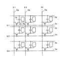
図2において、本実施形態における駆動回路は、データ線駆動回路101、走査線駆動回路104及びサンプリング回路301を備える。尚、図2では、図1に示した容量線3bは便宜上省略してある。
【0057】
データ線駆動回路101は、右シフト(左から右へ向かう右方向)用のシフトレジスタ101R及び左シフト(右から左へ向かう左方向)用のシフトレジスタ101Lを含んで構成されており、これらのシフトレジスタ101R又は101Lを選択的に動作させることにより、シフトレジスタ101Rからサンプリング回路301に対してサンプリング回路駆動信号XR1、XR2、…、XRnを右方向に順次供給するか、又はシフトレジスタ101Lからサンプリング回路301に対してサンプリング回路駆動信号XL1、XL2、…、XLnを、サンプリング回路駆動信号線116を介して左方向に順次供給するように構成されている。
【0058】
サンプリング回路301は、6本の画像信号線115(NO.1〜NO.6)に供給されるシリアル−パラレル変換された6つの画像信号VID1〜VID6をサンプリング回路駆動信号XRi又はXLi(但し、i=1、2、…、n)に応じて、サンプリングして、複数のデータ線6aに夫々供給する複数のサンプリングスイッチ302R及び302Lから構成されている。尚、本実施形態においてシリアル−パラレル変換される画像信号VID1〜VID6は、カラー画像信号でもよいし、白黒画像信号でもよい。
【0059】
走査線駆動回路104は、複数の走査線3aに対して走査信号G1、G2、…、Gmを供給するように構成されている。
【0060】
複数のサンプリングスイッチ302Rは、シフトレジスタ101Rから供給されるサンプリング回路駆動信号XRiにより駆動される。他方、複数のサンプリングスイッチ302Lは、シフトレジスタ101Lから供給されるサンプリング回路駆動信号XLiにより駆動される。各サンプリングスイッチ302Rの出力端子と各サンプリングスイッチ302Lの出力端子とは、複数のデータ線6aの各々に対して並列接続されている。そして特に、右方向にi(但し、iは自然数)番目のサンプリングスイッチ302Rと、左方向にi番目のサンプリングスイッチ302Lとは、同一の画像信号線115(即ち、6本のうちの同一の1本)に接続されている。例えば、左端(右方向に1番目)のサンプリングスイッチ302Rは、画像信号VID1が供給される画像信号線(NO.1)に接続されており、右端(左方向に1番目)のサンプリングスイッチ302Lも、同じく画像信号VID1が供給される画像信号線(NO.1)に接続されており、サンプリングスイッチ302Rと302Lとは、6本の画像信号線115について左右対称に接続されている。
【0061】
以上の如き構成において、外部の画像信号処理回路からシリアル−パラレル変換された6つの画像信号VID1〜VID6が6本の画像信号線115に供給され、走査線駆動回路104により、複数の走査線3aに対して走査信号G1、G2、…、Gmが供給される。
【0062】
ここで第1の場合として、シフトレジスタ101Rの転送動作をスタートさせるための選択信号の一例としてのスタート信号DX−Rを外部の画像信号処理回路又は制御回路から供給すれば、シフトレジスタ101Rが、水平走査用の基準クロック信号CLX及びその反転信号CLX’に基づいて転送動作を開始する。すると、サンプリング回路駆動信号XRiが、各サンプリング回路駆動信号線116を介して複数のサンプリングスイッチ302Rの配列に対して右方向に順次出力される(図3(a)参照)。この結果、サンプリング回路駆動信号XRiに応じて、サンプリングスイッチ302Rが駆動されて、複数の画像信号線115に供給されるシリアル−パラレル変換された画像信号VID1〜VID6がサンプリングされる。そして、各サンプリングスイッチ302Rの出力端子に接続された各データ線6aに、サンプリングされた画像信号VID1〜VID6が供給される。
【0063】
或いは第2の場合として、シフトレジスタ101Lの転送動作をスタートさせるための選択信号の一例としてのスタート信号DX−Lを外部の画像信号処理回路又は制御回路から供給すれば、シフトレジスタ101Lが、基準クロック信号CLX及びその反転信号CLX’に基づいて転送動作を開始する。すると、サンプリング回路駆動信号XLiが、各サンプリング回路駆動信号線116を介して、複数のサンプリングスイッチ302Lの配列に対して左方向に順次出力される(図3(b)参照)。この結果、サンプリング回路駆動信号XLiに応じて、サンプリングスイッチ302Lが駆動されて、複数の画像信号線115に供給されるシリアル−パラレル変換された画像信号VID1〜VID6がサンプリングされる。そして、各サンプリングスイッチ302Lの出力端子に接続された各データ線6aに、サンプリングされた画像信号VID1〜VID6が供給される。
【0064】
以上のように本実施形態では、右方向にi番目のサンプリングスイッチ302Rと、左方向にi番目のサンプリングスイッチ302Lとは、同一の画像信号線115に接続されているので、シフトレジスタ101Rを動作させて右方向にサンプリング回路駆動信号XRiを順次供給する場合と、シフトレジスタ101Lを動作させて左方向にサンプリング回路駆動信号XLiを順次供給する場合とでは、両端から数えて同一番目に当るデータ線6aには、各サンプリングスイッチ302R又は302Lを介して同一の画像信号線115からの画像信号VID1〜VID6が供給されることになる。このため、シリアル−パラレル変換された複数の画像信号VID1〜VID6内における各画像信号線115に対する各画像信号の順番を図14に示した如くに入れ換える必要なく、スタート信号DX−R又はDX−Lをデータ線駆動回路101に供給することにより、シフトレジスタ101Rを動作させるか又はシフトレジスタ101Lを動作させるかに応じて、水平走査方向を左右に反転させる。これにより、表示画像を左右に反転させることができる。
【0065】
他方、走査線駆動回路104は、走査方向が夫々下方向及び上方向の2個の単一方向シフトレジスタ若しくは双方向シフトレジスタを備えており、垂直走査方向を上下に反転可能に構成されている。即ち、単純に各走査線3aに順次供給する走査信号G1、G2、…、Gmの供給順序をシフトレジスタにより上下反転すれば、垂直走査方向を上下反転できる。より具体的には、走査線駆動回路104に含まれる2個の単一方向シフトレジスタのうちの下シフト用のシフトレジスタの転送動作又は1個の双方向シフトレジスタの下方向(下シフト)の転送動作をスタートさせるためのスタート信号DY−Dを外部の画像信号処理回路等から供給すれば、このシフトレジスタが、垂直走査用の基準クロック信号CLY及びその反転信号CLY’に基づいて転送動作を開始する。この結果、転送信号が走査信号G1、G2、…、Gmとして、下方向に順次出力される。或いは、走査線駆動回路104に含まれる2個の単一方向シフトレジスタのうちの上シフト用のシフトレジスタの転送動作又は1個の双方向シフトレジスタの上方向(上シフト)の転送動作をスタートさせるためのスタート信号DY−Uを外部の画像信号処理回路等から供給すれば、このシフトレジスタが、基準クロック信号CLY及びその反転信号CLY’に基づいて転送動作を開始する。この結果、転送信号が走査信号G1、G2、…、Gmとして、上方向に順次出力される。
【0066】
以上の結果、画像信号線115に対する画像信号VID1〜VID6の入れ換え動作という外部の画像信号処理回路の側における動作負担を伴うことなく、データ線駆動回路101及び走査線駆動回路104の側におけるシフトレジスタの切り換え動作という比較的簡単な動作を行えば、表示画像を左右や上下に反転させることができる。従って、既存の走査方向の反転機能を有しない電気光学装置用の画像信号処理回路と同一回路を用いても、表示画像の反転を実現できるので、装置全体のハードウエア構成や信号処理制御の簡略化を図る上で大変便利である。また、各サンプリングスイッチ302Rと各サンプリングスイッチ302Lとは並列接続されているので、各時点における画像信号VID1〜VID6に対して画像信号線115とデータ線6aとの間に介在するサンプリングスイッチ数は、従来通り夫々1個で済むと共に、この間に付加的なスイッチも必要としない。従って、従来と比べて画像信号線115からデータ線6aに至る配線や素子部分におけるインピーダンスを無用に高めないで済む。このため、画像信号劣化を抑制する観点、即ち表示画像の高品位化の観点からも有利である。
【0067】
本実施形態では特に、サンプリングスイッチ302Rとサンプリングスイッチ302Lとは、X方向に沿って交互に配置されており、相隣接する一対のサンプリングスイッチ302R及び302Lは、同一のデータ線6aに接続されている。このように、サンプリングスイッチ302R及び302Lは規則正しく交互に並べられており、サンプリング回路駆動信号用の配線や画像信号線115からサンプリングスイッチ302R及び302Lを介してデータ線6aに至る配線がコンパクトに納められた平面レイアウトが得られる。このコンパクトで各配線長さや交差個所が極力抑えられた平面レイアウトを採用することは、画像信号線115からデータ線6aに至る配線部分における画像信号VID1〜VID6の劣化(ノイズの混入)を低減する上で非常に有効である。
【0068】
また、本実施形態では、データ線駆動回路101、走査線駆動回路104及びサンプリング回路301を含む駆動回路は、後述のように液晶等の電気光学物質を挟持する一対の基板の一方上に形成されており、当該電気光学装置は、駆動回路内蔵型として構築されている。従って、本実施形態により、外部から入力すべき画像信号に対して画像信号処理回路の側で何らの変更を加えることなく、電気光学装置の側で表示画像を簡単に左右反転できる非常に便利な駆動回路内蔵型の電気光学装置を実現できる。
【0069】
更にまた、本実施形態では、シフトレジスタ101R及び101Lは、選択信号の一例たるスタート信号DX−R及びDX−Lに応じて一方が選択的に動作するように構成されているため、選択されない方のシフトレジスタを非動作状態にすることで、データ線駆動回路101における消費電力を低減させることができ、最終的には当該駆動回路全体の低消費電力化を図れる。
【0070】
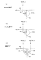
ここで、このように選択的に動作するシフトレジスタ101Rの具体的な二つの構成例について図4から図6を参照して説明する。ここに、図4(a)は、位相補正回路を備えない構成例であり、図4(b)は、位相補正回路を備える構成例である。また、シフトレジスタ101Lの具体的な構成については、シフトレジスタ101Rと左右対称であるため、その具体的な説明は省略する。更に、図5は、位相補正回路を用いた場合の転送信号等のタイミングチャートであり、図6は、シフトレジスタを構成するクロックドインバータの回路図である。
【0071】
図4(a)に示すように、シフトレジスタ101Lの一例は、各段毎に、クロック信号CLX及びその反転信号CLX’に基づいて転送信号を出力すると共に次段へ転送するクロックドインバータ401及びインバータ402並びに次段から転送信号の帰還を行うクロックドインバータ403を備えている。シフトレジスタ101Lの各段から出力される転送信号は、NAND回路501及びインバータ502等からなる各バッファ回路500に入力され、各バッファ回路500を介して各データ線(図2参照)に供給される。このバッファ回路500が介在していることにより、比較的低インピーダンスのサンプリングスイッチを比較的小サイズのトランジスタを用いて構成したシフトレジスタにより駆動することが可能となる。
【0072】
図4(b)に示すように、シフトレジスタ101Lの他の例は、図4(a)の例と比べて各段の転送出力の出力端子とバッファ回路との間に位相補正回路600を備えて構成されている点が異なる。その他の構成については、図4(a)の例と同様であるので、同様の参照符号を付しその説明は省略する。この位相補正回路600は、NAND回路601及びインバータ602から構成されており、図5に示すように、各段から出力されクロック信号CLXと同じパルス幅を持つ転送信号のパルス幅を夫々、位相補正信号ENB1及びENB2のパルス幅に制限して(奇数番目のサンプリング回路駆動信号のパルス幅を位相補正信号ENB1により制限すると共に偶数番目のサンプリング回路駆動信号のパルス幅を位相補正信号ENB2により制限して)、サンプリング回路駆動信号XR1、XR2、XR3、…として出力するように構成されている。これにより、相前後して出力されるサンプリング回路駆動信号XRiとXRi+1の間に若干の時間的マージンΔτが置かれることになる。従って、このシフトレジスタ回路101Rの例によれば、相前後して駆動される筈のサンプリングスイッチ302Rがサンプリング回路駆動信号XRiの立ち上がり及びサンプリング回路駆動信号XRi+1の立ち下がりの瞬間に重複してオン状態とされて、この時にサンプリングされた画像信号間にクロストークが生じたり、その結果表示画像にゴーストが生じたりする事態を未然に防ぐことが出来る。また、図4(a)のNAND回路を3端子で制御する3端子NAND回路にし、余った入力端子に位相補正信号を供給するようにすれば、図4(b)と同じ駆動を行うことができる。この場合、位相補正信号及び供給配線が1つで済むため有利である。
【0073】
次に、図4(a)及び図4(b)に示したシフトレジスタ回路101Rの各例を構成するクロックドインバータの具体的な回路構成を、図6に示す。ここに図6(a)は、一個のクロックドインバータの記号図であり、図6(b)は、その回路図である。
【0074】
図6(b)に示すように、クロックドインバータは、クロック信号CLがゲートに入力されるNチャネル型TFTと、その反転信号CL’が入力されるPチャネル型TFTと、ゲートに転送信号が夫々入力されるように並列に接続されたPチャネル型TFT及びNチャネル型TFTと、電源VSS(接地電位電源)及びVDD(ハイレベル電源)とが、図に示す如くに接続されている。このように各クロックドインバータは、電源VSS及びVDDを必要とするため、図2及び図4に示したシフトレジスタ全体としても電源配線を各クロックドインバータに引き回す必要がある。また、各クロックドインバータにおいては、入力端子と出力端子との間は各TFTのゲート絶縁膜により絶縁されているため、転送信号の周波数が高くても、転送方向に逆らって電流リークしない利点がある。従って、シフトレジスタ全体としても、高周波数に対して安定した転送信号を出力することが出来る利点がある。
【0075】
以上説明したシフトレジスタ101R及び101Lには、図2に示したように、共通のクロック信号CLX及びその反転信号CLX’が共に供給されている。このため、シフトレジスタ101R及び101Lに対して、データ線駆動回路101内に引き回されるクロック信号用の配線のパターンの簡略化が図れる。但し、データ線駆動回路101において、シフトレジスタ101R並びに101Lに対して個別のクロック信号CLX−R及びその反転信号CLX−R’並びにクロック信号CLX−L及びその反転信号CLX−L’が夫々供給されるように構成してもよい。このように構成すれば、一方のシフトレジスタによりサンプリングスイッチ302R又は302Lを駆動する際に、他方のシフトレジスタの動作をそれに供給されるクロック信号ごと停止させても、一方のシフトレジスタにおける動作には何等の支障も来たさない。従って、不要なシフトレジスタをクロック信号と共に非動作状態にすることで、データ線駆動回路101における消費電力を低減させることができる。
【0076】
次に、図2に示したサンプリング回路301を構成するサンプリングスイッチ302R及び302Lの具体的な回路構成を、図7(1)、(2)及び(3)の回路図に夫々示す。
【0077】
即ち、図7(1)に示すようにサンプリングスイッチは、Nチャネル型TFT302aから構成されてもよいし、図7(2)に示すようにPチャネル型TFT302bから構成されてもよいし、図7(3)に示すように相補型TFT302cから構成されてもよい。なお、図7(1)から図7(3)において、図2に示した画像信号線115を介して入力される画像信号VIDは、ソース電圧として各TFT302a〜302cに入力される。同じく図2に示したデータ線駆動回路101からサンプリング回路駆動信号線116を介して入力されるサンプリング回路駆動信号XRi(XLi)又はその反転信号XRi’(XLi’)は、ゲート電圧として各TFT302a〜302cに入力される。また、Nチャネル型TFT302aにゲート電圧として印加されるサンプリング回路駆動信号XRi(XLi)と、Pチャネル型TFT302bにゲート電圧として印加されるサンプリング回路駆動信号XRi’(XLi’)とは、相互に反転信号である。従って、サンプリングスイッチを相補型TFT302cで構成する場合には、サンプリング回路駆動信号XRi(XLi)、XRi’(XLi’)用のサンプリング回路駆動信号線116が少なくとも2本以上必要となる。また、各サンプリングスイッチは、製造効率等の観点から好ましくは、画素部におけるTFTと同一製造プロセスにより製造可能なNチャネル型、Pチャネル型、相補型等のTFTから構成される。
【0078】
以上詳細に説明したように、本実施形態における電気光学装置によれば、外部の画像信号処理回路から同一のシリアル−パラレル変換された画像信号を供給しながら、データ線駆動回路101や走査線駆動回路104の側における切り換え動作により、走査方向を左右や上下に反転できる。
【0079】
(電気光学装置の第2実施形態)
本発明による、例えば液晶装置からなる電気光学装置の第2実施形態について、特にデータ線駆動回路の構成を中心として、図8を参照して説明する。図8は、データ線駆動回路及びサンプリング回路のブロック図である。尚、図8に示した第2実施形態において図1から図7に示した第1実施形態と同様の構成要素については、同様の参照符号を付し、その説明は省略する。
【0080】
図8において、第2実施形態では第1実施形態とは異なり、一つのサンプリング回路駆動信号XRi又はXLiを用いて、6本の画像信号線115に夫々接続された相隣接する6個のサンプリングスイッチ302R又は6個のサンプリングスイッチ302Lを同時に駆動するように構成されている点が異なる。即ち、第1実施形態では、サンプリングスイッチ302R及び302Lによるサンプリング方式は、1本ずつ順次にサンプリングする方式であるが、第2実施形態では、シリアル−パラレル変換された画像信号VID1〜VID6を、シリアル−パラレル変換数に等しい数だけ同時にサンプリングする方式を採る。
【0081】
より具体的には図8において、シフトレジスタ101Rからの1本のサンプリング回路駆動信号線116’毎に、6個のサンプリングスイッチ302Rが並列に接続されており、シフトレジスタ101Lからの1本のサンプリング回路駆動信号線116’毎に、6個のサンプリングスイッチ302Lが並列に接続されている。
【0082】
このように第2実施形態の電気光学装置では、データ線を6本ずつ同時駆動するので、1本ずつ順次駆動する場合と比較して、各画像信号をサンプリングする時間を長く取れる。この結果、サンプリングスイッチ302R及び302Lの能力が低くてもサンプリングを行うことが可能となり有利である。
【0083】
尚、複数の画像信号線115は、一般には相互に平行に伸びる信号線群として基板上に配列されるが(図2及び図8参照)、この信号線群の一端側から他端側へ向けての配列順序は、これらが供給される複数のデータ線における配列順序の通りでもよいが、一般に任意である。
【0084】
即ち、第1及び第2実施形態の場合と同じく図9(a)に示すように、画像信号VID1〜VID6を供給する各画像信号線の順番をデータ線の配列順序の通りに配列してもよいし、図9(b)に示すように、画像信号VID1〜VID6を供給する各画像信号線115’の順番をデータ線の配列順序と逆順に配列してもよいし、或いは、図9(c)に示すように、画像信号VID1〜VID6を供給する各画像信号線115”の順番をデータ線の配列順序に対して適当に入れ替えた順に配列してもよい。いずれの場合にも、サンプリングスイッチ302Rの配列に接続される画像信号線の順番とサンプリングスイッチ302Lの配列に接続される画像信号線の順番とが左右対称となっている限り上述した各実施形態独自の効果は奏される。
【0085】
尚、上述の実施形態では、画像信号線を6本用いることを例として説明したが、これに限らず、12本、24本等の自然数に適宜画像信号線の本数を増やすことも可能である。
【0086】
(電気光学装置の全体構成)
以上のように構成された、例えば液晶装置からなる電気光学装置の各実施形態の全体構成を図10及び図11を参照して説明する。尚、図10は、TFTアレイ基板10をその上に形成された各構成要素と共に対向基板20の側から見た平面図であり、図11は、対向基板20を含めて示す図10のH−H’断面図である。
【0087】
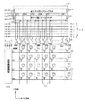
図10及び図11において、電気光学装置は、対向配置されたTFTアレイ基板10及び対向基板20を備えており、TFTアレイ基板10上には、図1から図9を参照して説明した画素電極9a、データ線駆動回路101及び走査線駆動回路104並びに走査線、データ線、TFT等が形成されている。画素電極9aと対向電極21とが対面するように配置されたTFTアレイ基板10と対向基板20との間には、シール材52により囲まれた空間に電気光学物質が封入され、電気光学物質層50が形成される。電気光学物質層50は、画素電極9aからの電界が印加されていない状態で両基板の電気光学物質層50に面する表面に夫々形成された配向膜により所定の配向状態をとる。電気光学物質層50は、例えば一種又は数種類のネマティック電気光学物質を混合した電気光学物質からなる。シール材52は、TFTアレイ基板10及び対向基板20をそれらの周辺で貼り合わせるための、例えば光硬化性樹脂や熱硬化性樹脂からなる接着剤であり、両基板間の距離を所定値とするためのグラスファイバー或いはガラスビーズ等のスペーサが混入されている。
【0088】
対向基板20には、各画素の開口領域以外の領域に、遮光膜が設けられても良いし、TFTアレイ基板10上に形成しても良い。このため、対向基板20の側から入射光が画素スイッチング用TFTに侵入することはない。更に、この遮光膜は、コントラストの向上、色材の混色防止などの機能を有する。
【0089】
また、TFTアレイ基板10の上には、シール材52の内側に並行して、例えば上述の遮光膜と同じ或いは異なる材料から成る額縁としての遮光膜53が設けられている。
【0090】
更に、シール材52の外側の領域には、データ線駆動回路101及び外部回路接続端子102がTFTアレイ基板10の一辺に沿って設けられており、走査線駆動回路104が、この一辺に隣接する2辺に沿って設けられている。走査線3aに供給される走査信号遅延が問題にならないのならば、走査線駆動回路104は片側だけでも良いことは言うまでもない。また、データ線駆動回路101を画像表示領域の辺に沿って両側に配列してもよい。
【0091】
図12に示すように、例えば奇数列のデータ線6aは画像表示領域の上辺に沿って配設された右シフト用シフトレジスタ101Ra及び左シフト用シフトレジスタ101Laを含むデータ線駆動回路から画像信号を供給し、偶数列のデータ線は前記画像表示領域の下辺に沿って配設された右シフト用シフトレジスタ101Rb及び左シフト用シフトレジスタ101Lbを含むデータ線駆動回路から画像信号を供給するようにしてもよい。この様にデータ線6aに画像信号を供給する配線及び回路構成を上下に櫛歯状に構成すれば、データ線駆動回路の占有面積を拡張することができるため、複雑な回路を構成することが可能となる。つまり、奇数番目のデータ線6aに係るこれらの回路部分を一方の周辺領域に配置すると共に偶数番目のデータ線6aに係るこれらの回路部分を他方の周辺領域に配置する構成を採れば、データ線6aの配列ピッチの2倍のピッチでこれらの回路を形成すればよいので、データ線6aの配列ピッチを狭めて画素の微細化を図る上で有利である。
【0092】
図10及び図11において、更にTFTアレイ基板10の残る一辺には、画像表示領域の両側に設けられた走査線駆動回路104間をつなぐための複数の配線105が設けられている。また、対向基板20のコーナー部の少なくとも1箇所においては、TFTアレイ基板10と対向基板20との間で電気的導通をとるための導通材106が設けられている。尚、図2及び図8などに示したサンプリング回路301は、図10では、例えば額縁53の下に隠れる位置におけるTFTアレイ基板10上に設けられている。
【0093】
各実施形態では、このようにデータ線駆動回路101及びサンプリング回路301は、一部が画像表示領域の一方の周辺領域に設けられており、これに対向する他方の周辺領域に他部が設けられてもよい。このように構成すれば、データ線駆動回路101及びサンプリング回路を画像表示領域の周囲にバランス良く配置することが可能となる。同様に、走査線駆動回路104は、一部が画像表示領域の一方の周辺領域に設けられており、これに対向する他方の周辺領域に他部が設けられてもよい。このように構成すれば、データ線6aの配列ピッチや走査線3aの配列ピッチを狭めて画素の微細化を図る上で有利である。
【0094】
以上図1から図11を参照して説明した各実施形態における電気光学装置のTFTアレイ基板10上には更に、画像信号のデータ線6aへの書込み負荷軽減のために各データ線6aについて画像信号に先行するタイミングで所定電位のプリチャージ信号を書き込むプリチャージ回路を形成してもよいし、製造途中や出荷時の当該電気光学装置の品質、欠陥等を検査するための検査回路等を形成してもよい。また、データ線駆動回路101、走査線駆動回路104等の周辺回路の一部又は全部を、TFTアレイ基板10の上に設ける代わりに、例えばTAB(Tape Automated Bonding)上に実装された駆動用LSIに、TFTアレイ基板10の周辺部に設けられた異方性導電フィルムを介して電気的及び機械的に接続するようにしてもよい。
【0095】
また、以上の各実施形態において、特開平9−127497号公報、特公平3−52611号公報、特開平3−125123号公報、特開平8−171101号公報等に開示されているように、TFTアレイ基板10上においてTFT30に対向する位置(即ち、TFT30の下側)にも、例えば高融点金属からなる遮光膜を設けてもよい。このようにTFT30の下側にも遮光膜を設ければ、TFTアレイ基板1の側からの戻り光等がTFT30に入射するのを未然に防ぐことができる。
【0096】
更にまた、対向基板20の投射光が入射する側及びTFTアレイ基板10の出射光が出射する側には各々、例えば、TN(ツイステッドネマティック)モード、 STN(スーパーTN)モード、D−STN(ダブル−STN)モード等の動作モードや、ノーマリーホワイトモード/ノーマリーブラックモードの別に応じて、偏光フィルム、位相差フィルム、偏光板などが所定の方向で配置される。
【0097】
以上説明した各実施形態における電気光学装置は、カラープロジェクタに適用されるため、3枚の電気光学装置がRGB用のライトバルブとして各々用いられ、各パネルには各々RGB色分解用のダイクロイックミラーを介して分解された各色の光が投射光として各々入射されることになる。従って、実施の形態では、対向基板20に、カラーフィルタは設けられていない。しかしながら、遮光膜23の形成されていない画素電極9aに対向する所定領域にRGBのカラーフィルタをその保護膜と共に、対向基板20上に形成してもよい。このようにすれば、プロジェクタ以外の直視型や反射型のカラー液晶テレビなどのカラー電気光学装置に実施の形態における電気光学装置を適用できる。更に、対向基板20上に1画素1個対応するようにマイクロレンズを形成してもよい。このようにすれば、入射光の集光効率を向上することで、明るい電気光学装置が実現できる。更にまた、対向基板20上に、何層もの屈折率の相違する干渉層を堆積することで、光の干渉を利用して、RGB色を作り出すダイクロイックフィルタを形成してもよい。このダイクロイックフィルタ付き対向基板によれば、より明るいカラー電気光学装置が実現できる。
【0098】
また、各画素に設けられるスイッチング素子としては、正スタガ型又はコプラナー型のポリシリコンTFTでよいが、逆スタガ型のTFTやアモルファスシリコンTFT等の他の形式のTFTに対しても、各実施形態は有効である。
【0099】
(電子機器)
次に、以上詳細に説明した電気光学装置を備えた電子機器の実施の形態について図15から図17を参照して説明する。
【0100】
先ず図15に、このように電気光学装置の一例として液晶装置100を備えた電子機器の概略構成を示す。
【0101】
図15において、電子機器は、表示情報出力源1000、表示情報処理回路1002、駆動回路1004、液晶装置100、クロック発生回路1008並びに電源回路1010を備えて構成されている。表示情報出力源1000は、ROM(Read Only Memory)、RAM(Random Access Memory)、光ディスク装置などのメモリ、画像信号を同調して出力する同調回路等を含み、クロック発生回路1008からのクロック信号に基づいて、所定フォーマットの画像信号などの表示情報を表示情報処理回路1002に出力する。表示情報処理回路1002は、増幅・極性反転回路、シリアル−パラレル変換回路、ローテーション回路、ガンマ補正回路、クランプ回路等の周知の各種処理回路を含んで構成されており、クロック信号に基づいて入力された表示情報からデジタル信号を順次生成し、クロック信号CLKと共に駆動回路1004に出力する。駆動回路1004は、液晶装置100を駆動する。電源回路1010は、上述の各回路に所定電源を供給する。尚、液晶装置100を構成するTFTアレイ基板の上に、駆動回路1004を搭載してもよく、これに加えて表示情報処理回路1002を搭載してもよい。
【0102】
次に図16から図17に、このように構成された電子機器の具体例を各々示す。
【0103】
図16において、電子機器の一例たる液晶プロジェクタ1100は、上述した駆動回路1004がTFTアレイ基板上に搭載された液晶装置100を含む液晶表示モジュールを3個用意し、各々RGB用のライトバルブ100R、100G及び100Bとして用いたプロジェクタとして構成されている。液晶プロジェクタ1100では、メタルハライドランプ等の白色光源のランプユニット1102から投射光が発せられると、3枚のミラー1106及び2枚のダイクロイックミラー1108によって、RGBの3原色に対応する光成分R、G、Bに分けられ、各色に対応するライトバルブ100R、100G及び100Bに各々導かれる。この際特にB光は、長い光路による光損失を防ぐために、入射レンズ1122、リレーレンズ1123及び出射レンズ1124からなるリレーレンズ系1121を介して導かれる。そして、ライトバルブ100R、100G及び100Bにより各々変調された3原色に対応する光成分は、ダイクロイックプリズム1112により再度合成された後、投射レンズ1114を介してスクリーン1120にカラー画像として投射される。
【0104】
図17において、電子機器の他の例たるマルチメディア対応のラップトップ型のパーソナルコンピュータ1200は、上述した液晶装置100がトップカバーケース内に設けられており、更にCPU、メモリ、モデム等を収容すると共にキーボード1202が組み込まれた本体1204を備えている。
【0105】
以上図16から図17を参照して説明した電子機器の他にも、液晶テレビ、ビューファインダ型又はモニタ直視型のビデオテープレコーダ、カーナビゲーション装置、電子手帳、電卓、ワードプロセッサ、エンジニアリング・ワークステーション(EWS)、携帯電話、テレビ電話、POS端末、タッチパネルを備えた装置等などが図15に示した電子機器の例として挙げられる。
【0106】
以上説明したように、本実施の形態によれば、製造効率が高く高品位の画像表示が可能な液晶装置を備えた各種の電子機器を実現できる。
【0107】
【発明の効果】
本発明によれば、シリアル−パラレル変換された画像信号を複数の画像信号線を介して供給する画像信号処理回路の側では画像信号を等しく供給しつつも、表示画像を簡単に反転できる。即ち、画像信号線に対する画像信号の入れ換え動作という外部の画像信号処理回路の側における動作負担を伴うことなく、電気光学装置の駆動回路の側における比較的簡単な切り換え動作を行えば、表示画像を左右や上下に反転させることができる。従って、既存の走査方向の反転機能を有しない電気光学装置用の画像信号処理回路と同一回路を用いても、表示画像の反転を実現できるので、装置全体のハードウエア構成や信号処理制御の簡略化を図る上で大変便利である。
【図面の簡単な説明】
【図1】電気光学装置の第1実施形態における画像表示領域を構成するマトリクス状の複数の画素に設けられた各種素子、配線等の等価回路である。
【図2】電気光学装置の第1実施形態における駆動回路を含む全体回路構成を示すブロック図である。
【図3】図2に示したデータ線駆動回路を構成する各シフトレジスタにおける各種信号のタイミングチャートである。
【図4】図2に示したデータ線駆動回路を構成する各シフトレジスタの具体的な構成例を示す回路図である。
【図5】図4(b)に示したシフトレジスタにおける各種信号のタイミングチャートである。
【図6】図4に示したシフトレジスタの構成例に含まれるクロックドインバータの詳細な回路図である。
【図7】図2に示したサンプリング回路に含まれるサンプリングスイッチの各種構成例を示す回路図である。
【図8】電気光学装置の第2実施形態におけるデータ線駆動回路のブロック図である。
【図9】電気光学装置の各実施形態における画像信号線とサンプリングスイッチとの接続方式の各種具体例を示す配線図である。
【図10】電気光学装置の各実施形態におけるTFTアレイ基板をその上に形成された各構成要素と共に対向基板の側から見た平面図である。
【図11】図10のH−H’断面図である。
【図12】電気光学装置の一変形形態におけるデータ線駆動回路のブロック図である。
【図13】プロジェクタのRGBの3色光を合成するプリズム光学系を示す概念図である。
【図14】シリアル−パラレル変換された画像信号による表示画像を反転する際に必要な該画像信号の入れ換え方式を示す概念図である。
【図15】本発明による電子機器の実施の形態の概略構成を示すブロック図である。
【図16】電子機器の一例として液晶プロジェクタを示す断面図である。
【図17】電子機器の他の例としてパーソナルコンピュータを示す正面図である。
【符号の説明】
3a…走査線
3b…容量線
6a…データ線
9a…画素電極
10…TFTアレイ基板
20…対向基板
21…対向電極
30…画素スイッチング用TFT
50…電気光学物質層
52…シール材
53…遮光膜
70…蓄積容量
101…データ線駆動回路
101R、101L…シフトレジスタ
104…走査線駆動回路
115…画像信号線
116…サンプリング回路駆動信号線
301…サンプリング回路
302R、302L…サンプリングスイッチ
500…バッファ回路
600…位相補正回路[0001]
BACKGROUND OF THE INVENTION
The present invention relates to a driving circuit for an electro-optical device (for example, a liquid crystal device, etc.) such as an active matrix driving method by driving a thin film transistor (hereinafter appropriately referred to as TFT), a thin film diode (hereinafter appropriately referred to as TFD), and the like. It belongs to the technical field of an electro-optical device having a built-in circuit, and particularly belongs to the technical field of a drive circuit for an electro-optical device that is preferably used as a light valve of a projector.
[0002]
[Prior art]
Conventionally, when an electro-optical device such as a liquid crystal device is used as a light valve of this type of projector, a single plate method using only one electro-optical device having a color filter formed on a counter substrate and a color filter are formed. There is a double plate system using three electro-optical devices for each of RGB. The single plate method is simple in structure, but the double plate method is more excellent in that the display screen is brightened and a high quality image can be obtained. According to this double plate system, the three color lights separately modulated by the three electro-optical devices are combined into one projection light by the prism or dichroic mirror, and then projected onto the screen.
[0003]
In this way, when combined by a prism or the like, for example, as shown in FIG. 13, compared to the R light and B light reflected by the
[0004]
On the other hand, depending on the product strategy, you may want to configure the projector so that it can be used as a floor-mounted projector that is normally installed on the floor or as a ceiling-mounted projector that is installed upside down on the ceiling. . In this case, even in the single plate method, it is necessary to invert the image signal supplied to the electro-optical device vertically and horizontally depending on the installation method. In addition, there may be a case where a liquid crystal monitor, which is a single-plate electro-optical device, such as a liquid crystal monitor of a portable video camera, is desired to be viewed, for example, with a flexible joint as a fulcrum according to the user's shooting posture. . In this case, the image signal supplied to the electro-optical device needs to be reversed in the vertical and horizontal directions in some way.
[0005]
Therefore, conventionally, an image signal processing IC that supplies an image signal in a predetermined format to a data line driving circuit in an electro-optical device, for example, only an image signal for G or an image signal for all colors is converted into an original image. On the other hand, an image signal corresponding to an inverted image is generated and supplied for each field. This is convenient because it is not necessary to make any changes to the electro-optical device or the drive circuit.
[0006]
Alternatively, conventionally, for example, in order to synthesize three-color light as described above, an electro-optical device whose scanning direction is reversed left and right as compared with the electro-optical device for R and the electro-optical device for B is used for G. It is used as an electro-optical device.
[0007]
[Problems to be solved by the invention]
However, the method of inverting an image signal vertically and horizontally using the above-described conventional image signal processing IC is too heavy on the image signal processing IC in order to cope with a recent high-quality image. It is no longer practical.
[0008]
In addition, the method using the G electro-optical device whose scanning direction is inverted vertically and horizontally has the following problems. That is, in general, the scanning line driving circuit and the data line driving circuit have a unidirectional shift register in which the transfer direction is fixed to one side, and the line sequential or the data line driving circuit is based on the transfer signal generated from the unidirectional shift register. A scanning signal or an image signal is supplied in a dot sequential manner, and the display screen is scanned vertically and horizontally. Therefore, in order to use the electro-optical device for G whose scanning direction is reversed, an R-shift electro-optical device in which a shift register is configured so that the data line driving circuit scans the display screen from left to right; Therefore, there is a need to manufacture two types of L-shift type electro-optical devices in which a shift register is configured so that the data line driving circuit scans the display screen from right to left. Thus, it is clearly disadvantageous from the manufacturer's standpoint to manufacture two types of electro-optical devices in a TFT manufacturing process or the like using, for example, a semiconductor manufacturing device or the like. Also, from the user's standpoint, there is no compatibility between similar electro-optical devices, and there is a practical problem that any individual device can be used only as either type. Furthermore, the electro-optical device with the scanning direction fixed as described above realizes a projector that can be used as the above-mentioned floor-mounted type or ceiling-mounted type, and a portable video camera liquid crystal monitor whose screen is inverted vertically and horizontally. Can not.
[0009]
Also, if the scanning line driving circuit and the data line driving circuit adopt a bidirectional shift register so that the transfer direction of the output transfer signal is reversed up and down or left and right, the supply order of the scanning signal and image signal can be changed. It is possible to invert, that is, to invert the horizontal scanning direction and the vertical scanning direction vertically and horizontally. However, if a bi-directional shift register is used, the number of gates constituting the shift register is larger than that in the case of the unidirectional shift register described above. There is a problem that electric power increases.
[0010]
Furthermore, if a bidirectional shift register is adopted, especially when performing display using an image signal subjected to serial-parallel conversion, a plurality of image signal lines are provided in accordance with reversing the horizontal scanning direction of the image signal. On the other hand, there is a problem that it is necessary to change the order of the image signals supplied in parallel.
[0011]
More specifically, for example, as shown in the upper half of FIG. 14, consider a case where image signals VID1 to VID6 subjected to serial-parallel conversion are supplied. In this case,
[0012]
As described above, if a bi-directional shift register is adopted, there is little problem if it is a single-phase image signal, but serial-parallel conversion has been performed to support the recent high-definition display and high dot frequency. If it is an image signal, it is necessary to change the order of the image signal to be supplied in parallel on the image signal processing IC side with respect to each image signal line, and if the same image signal is simply supplied to the electro-optical device, the entire image is reversed. There is a problem that the function of cannot be achieved.
[0013]
The present invention has been made in view of the above-described problems, and while an image signal processing circuit that supplies serial-parallel converted image signals via a plurality of image signal lines supplies image signals equally, It is an object of the present invention to provide an electro-optical device driving circuit capable of easily inverting a display image and an electro-optical device incorporating the driving circuit.
[0014]
[Means for Solving the Problems]
In order to solve the above problems, the drive circuit of the electro-optical device of the present invention samples serial-parallel converted image signals supplied to a plurality of image signal lines on the substrate in accordance with the sampling circuit drive signal. A sampling circuit composed of a plurality of sampling switches that respectively supply the plurality of data lines;
A data line driving circuit for supplying the sampling circuit driving signal to the sampling circuit,
The data line driving circuit includes: a first shift register that sequentially outputs the sampling circuit driving signal in a predetermined direction with respect to the plurality of sampling switches; and a direction opposite to the predetermined direction with respect to the plurality of sampling switches. A second shift register that sequentially outputs the sampling circuit driving signal in a direction,
The plurality of sampling switches include a first group driven by a sampling circuit drive signal supplied from the first shift register, and a second group driven by a sampling circuit drive signal supplied from the second shift register. The output terminal of each sampling switch included in the first group and the output terminal of each sampling switch included in the second group are connected in parallel to each of the plurality of data lines. It is characterized by that.
[0015]
The present invention also provides an electro-optical device for driving an electro-optical device having a plurality of data lines and a plurality of scanning lines that are sandwiched between a pair of substrates and that intersect each other on the substrate. A sampling circuit comprising a plurality of sampling switches, each of which is a driving circuit and samples a serial-parallel converted image signal supplied to a plurality of image signal lines in accordance with a sampling circuit driving signal and supplies the sampling signal to the plurality of data lines. And a data line driving circuit for supplying the sampling circuit driving signal to the sampling circuit, wherein the data line driving circuit is arranged in a predetermined direction with respect to the array of the plurality of sampling switches. A first shift register that sequentially outputs a drive signal; and A second shift register that sequentially outputs the sampling circuit drive signal in the opposite direction, and the plurality of sampling switches are driven by the sampling circuit drive signal supplied from the first shift register; And a second group driven by a sampling circuit driving signal supplied from the second shift register, and an output terminal of each sampling switch included in the first group and each sampling included in the second group The switch output terminal is connected in parallel to each of the plurality of data lines.
[0016]
According to the drive circuit of the electro-optical device of the present invention, an image signal that has been subjected to serial-parallel conversion is supplied from an external image signal processing circuit to the plurality of image signal lines. For example, six image signals VID1 to VID6 subjected to serial-parallel conversion are supplied to six image signal lines.
[0017]
Here, in the first case, if the first shift register of the data line driving circuit is operated in parallel with the scanning signal supply operation, the sampling circuit driving signal is transmitted in a predetermined direction with respect to the arrangement of the plurality of sampling switches ( For example, serial-to-parallel conversion is output sequentially from left to right ("right direction") and the sampling switch of the first group is driven in accordance with the sampling circuit drive signal and supplied to a plurality of image signal lines. The processed image signal is sampled. The sampled image signal is supplied to each data line connected to the output terminal of each sampling switch of the first group (in parallel with the output terminal of each sampling switch of the second group).
[0018]
Alternatively, in the second case, if the second shift register of the data line driving circuit is operated in parallel with the scanning signal supply operation, the sampling circuit driving signal is in a direction opposite to the predetermined direction (for example, from right to left). Are output sequentially in the “left direction”), and in response to the sampling circuit drive signal, the second group of sampling switches are driven and serial-parallel converted image signals supplied to the plurality of image signal lines are output. Sampled. The sampled image signal is supplied to each data line connected to the output terminal of each sampling switch of the second group (in parallel with the output terminal of each sampling switch of the first group).
[0019]
Therefore, when the first shift register is operated and the sampling circuit drive signal is sequentially supplied in a predetermined direction, and when the second shift register is operated and the sampling circuit drive signal is sequentially supplied in the opposite direction, the both are counted from both ends. An image signal can be supplied to the same data line from the same image signal line via each sampling switch. Therefore, the horizontal shift according to whether the first shift register is operated or the second shift register is operated without changing the order of the image signals for the image signal lines in the plurality of serial-parallel converted image signals. By reversing the scanning direction left and right, the display image can be reversed left and right.
[0020]
As described above, the predetermined switching operation on the drive circuit side of the electro-optical device (that is, the shift to be operated) is performed without the operation burden on the external image signal processing circuit side of the image signal replacement operation with respect to the image signal line. If a relatively simple operation (register switching operation) is performed, the display image can be reversed left and right by left and right reversal in the horizontal scanning direction.
[0021]
In the vertical scanning direction, there is no complicated signal supply such as serial-parallel conversion. For this reason, if necessary, the supply order of the scanning signals to be sequentially supplied to each scanning line simply using a bidirectional shift register or two unidirectional shift registers whose scanning directions are downward and upward respectively. The vertical scanning direction can be reversed up and down, so that the horizontal scanning direction and vertical scanning direction can be reversed left and right and up and down. A drive circuit for an invertible electro-optical device can be realized.
[0022]
In one aspect of the drive circuit of the electro-optical device of the present invention, the i-th sampling switch in the predetermined direction in the first group (where i is a natural number) and the i-th sampling switch in the opposite direction in the second group. The sampling switch is connected to the same image signal line.
[0023]
According to this aspect, the i-th sampling switch in a predetermined direction (for example, right direction) in the first group and the i-th sampling switch in the reverse direction (for example, left direction) in the second group are the same image. When connected to the signal line, the first shift register is operated to sequentially supply the sampling circuit drive signal in a predetermined direction, and the second shift register is operated to sequentially supply the sampling circuit drive signal in the reverse direction. In this case, the image signal from the same image signal line is reliably supplied to the data line corresponding to the same number from both ends via each sampling switch. Therefore, the horizontal shift according to whether the first shift register is operated or the second shift register is operated without changing the order of the image signals for the image signal lines in the plurality of serial-parallel converted image signals. By reversing the scanning direction to the left and right, the display image can be reliably reversed to the left and right.
[0024]
In another aspect of the drive circuit of the electro-optical device according to the aspect of the invention, the sampling switches belonging to the first group and the sampling switches belonging to the second group are alternately arranged along the predetermined direction, A pair of sampling switches belonging to the first and second groups and adjacent to each other are connected to the same data line.
[0025]
According to this aspect, the pair of adjacent sampling switches connected in parallel to the same data line are regularly and alternately arranged between the first and second groups, and the wiring for the sampling circuit drive signal and the image signal line A plane layout is obtained in which wiring from the data line to the data line via the sampling switch is compactly accommodated.
[0026]
In another aspect of the drive circuit of the electro-optical device according to the aspect of the invention, the image signal lines include n (n is a natural number), and the n images connected to the adjacent n in the first group. The order of the signal lines and the order of the n image signal lines connected to the n adjacent ones of the second group are right and left.
[0027]
According to this aspect of the present invention, the order of the n image signal lines connected to the n adjacent ones of the first group and the n adjacent ones of the second group are connected. Since the order of the n image signal lines is the right and left, the display image can be simplified without any change on the image signal processing circuit side with respect to the image signal to be input from the outside. You can flip left and right.
[0028]
In another aspect of the drive circuit of the electro-optical device of the present invention, one sampling circuit drive signal line that supplies a sampling circuit drive signal from the first shift register is connected to n sampling switches adjacent to the first group. One sampling circuit driving signal line connected in parallel and supplying a sampling circuit driving signal from the second shift register is connected in parallel to the n sampling switches adjacent to the second group. To do.
[0029]
According to such a configuration of the present invention, since n data lines are driven simultaneously, it is possible to take a longer time to sample each image signal than in the case where the data lines are sequentially driven one by one. As a result, it is possible to perform sampling even if the capability of the sampling switch is low.
[0030]
In another aspect of the drive circuit of the electro-optical device of the present invention, the drive circuit is formed on the substrate.
[0031]
According to this aspect, in the electro-optical device with a built-in drive circuit in which the drive circuit is formed on the substrate of the electro-optical device, the display image can be easily reversed left and right.
[0032]
In another aspect of the drive circuit of the electro-optical device of the present invention, one of the first and second shift registers operates selectively according to a selection signal.
[0033]
According to this aspect, for example, if a selection signal for selectively operating the first or second shift register is supplied from the outside, the first or second shift register operates in response to this, and the corresponding first Alternatively, the sampling operation is performed by the second group sampling switch. Therefore, the horizontal scanning direction is set to the right or left according to the selection signal. Further, by disabling the shift register that is not selected, the power consumption in the data line driver circuit can be reduced, and ultimately the power consumption of the entire driver circuit can be reduced.
[0034]
In another aspect of the drive circuit of the electro-optical device according to the aspect of the invention, the first and second shift registers are respectively supplied with individual clock signals serving as a reference for the generation timing of the sampling circuit drive signal.
[0035]
According to this aspect, since the individual clock signals are respectively supplied to the first and second shift registers, when the first or second group sampling switch is driven by one shift register, the other shift register is supplied. Even if this operation is stopped together with the clock signal supplied thereto, there is no problem in the operation of one shift register. Accordingly, by disabling unnecessary shift registers together with the clock signal, power consumption in the data line driver circuit can be reduced, and finally, the power consumption of the entire driver circuit can be reduced.
[0036]
Alternatively, the first and second shift registers may be supplied together with a common clock signal serving as a reference for the generation timing of the sampling circuit drive signal.
[0037]
With this configuration, since the common clock signal is supplied to the first and second shift registers, the wiring pattern for the clock signal routed in the scanning line driving circuit can be simplified.
[0038]
In another aspect of the drive circuit of the electro-optical device according to the aspect of the invention, the electro-optical device further includes a scan line drive circuit that supplies a scan signal to the scan line, and the scan line drive circuit applies the scan line to the plurality of scan lines. A third shift register that sequentially outputs the scanning signal; and a fourth shift register that sequentially outputs the scanning signal in a direction opposite to the direction in which the scanning signal is sequentially output from the third shift register.
[0039]
According to this aspect, when the third shift register is operated, the scanning line driving circuit can perform vertical scanning in which the vertical scanning direction is a predetermined direction (for example, the downward direction from the top to the bottom). If the fourth shift register is operated, vertical scanning can be performed in which the vertical scanning direction is the opposite direction (for example, the upward direction from the bottom to the top). Therefore, the vertical scanning direction can be reversed up and down depending on whether the third shift register is operated or the fourth shift register is operated. As a result, by selectively operating the first and second shift registers and the third and fourth shift registers, the scanning direction can be reversed up and down and left and right, and the display image can be turned up and down and left and right by switching the operation in the drive circuit. It can be easily reversed.
[0040]
In another aspect of the drive circuit of the electro-optical device according to the aspect of the invention, the image display region is provided at the center on the substrate, and the first and second data line drive circuits are provided on one side of the periphery on the substrate. A shift register is arranged.
[0041]
According to this aspect, since the first and second shift registers are provided on one side of the substrate, the wiring for the sampling circuit driving signal and the wiring from the image signal line to the data line through the sampling switch are stored compactly. A planar layout is obtained. Further, it is effective in reducing the deterioration of the image signal in the wiring portion from the image signal line to the data line.
[0042]
In another aspect of the drive circuit of the electro-optical device according to the aspect of the invention, an image display area is provided at a central portion on the substrate, and the data line drive circuit and the sampling circuit are partially displayed on the substrate. It is provided in one peripheral area of the area, and the other part is provided in the other peripheral area facing the one peripheral area with the image display area interposed therebetween on the substrate.
[0043]
According to this aspect, the data line driving circuit and the sampling circuit can be arranged in a well-balanced manner around the image display area. In particular, if the circuit portions related to the odd-numbered data lines are arranged in one peripheral region and the circuit portions related to the even-numbered data lines are arranged in the other peripheral region, the pitch of the data lines is increased. Since these circuits need only be formed at twice the pitch, it is advantageous in reducing the data line pitch and miniaturizing the pixels.
[0044]
Alternatively, an image display area is provided at a central portion on the substrate, and a part of the scanning line driving circuit is provided on one peripheral region of the image display area on the substrate, and the other part is the substrate. It is provided in the other peripheral area facing the one peripheral area with the image display area interposed therebetween.
[0045]
With this configuration, it is possible to arrange the scanning line driving circuit in a balanced manner around the image display area. In particular, if the circuit portion related to the odd-numbered scanning line is arranged in one peripheral region and the circuit portion related to the even-numbered scanning line is arranged in the other peripheral region, the arrangement pitch of the scanning lines is 2 Since it is sufficient to form this circuit with a double pitch, it is advantageous for reducing the arrangement pitch of the scanning lines and miniaturizing the pixels.
[0046]
In order to solve the above-described problems, the electro-optical device of the present invention incorporates a drive circuit for the electro-optical device according to the various aspects of the present invention described above.
[0047]
According to the electro-optical device of the present invention, since the above-described drive circuit of the present invention is incorporated, the same serial-parallel converted image signal is supplied from the external image signal processing circuit while the drive circuit side. The horizontal scanning direction can be reversed left and right by the switching operation at. Therefore, it is possible to construct an electro-optical device system that can invert a display image using an existing image signal processing circuit.
[0048]
In one aspect of the electro-optical device of the present invention, the plurality of pixel electrodes arranged in a matrix on the substrate, the plurality of scanning lines, and the plurality of data lines are electrically connected to the plurality of pixel electrodes, respectively. And a plurality of thin film transistors that selectively supply the image signals to a plurality of pixel electrodes in response to the scanning signals.
[0049]
According to this aspect, it is possible to realize an electro-optical device with a built-in driving circuit of a TFT active matrix driving system that can easily invert a serial-parallel converted display image.
[0050]
Such an operation and other advantages of the present invention will become apparent from the embodiments described below.
[0051]
DETAILED DESCRIPTION OF THE INVENTION
Hereinafter, embodiments of the present invention will be described with reference to the drawings.
[0052]
(First embodiment of electro-optical device)
A first embodiment of an electro-optical device including a liquid crystal device according to the present invention will be described with reference to FIGS.
[0053]
First, the configuration of the electro-optical device in the image display area will be described with reference to FIG. FIG. 1 is an equivalent circuit of various elements, wirings, and the like in a plurality of pixels formed in a matrix that constitutes an image display region of the electro-optical device.
[0054]
In FIG. 1, a plurality of pixels formed in a matrix form constituting the image display area of the electro-optical device according to the present embodiment has a plurality of
[0055]
Next, the configuration and operation of the drive circuit of the electro-optical device provided around the image display area will be described with reference to FIGS. FIG. 2 is a block diagram showing the electro-optical device according to the embodiment including a drive circuit, an image signal line, and the like provided on the substrate. FIG. 3 is a timing diagram of various signals in the data line drive circuit. It is a chart.
[0056]
In FIG. 2, the drive circuit in this embodiment includes a data
[0057]
The data line driving
[0058]
The
[0059]
The scanning
[0060]
The plurality of sampling switches 302R are driven by a sampling circuit drive signal XRi supplied from the
[0061]
In the configuration as described above, six image signals VID1 to VID6 serial-parallel converted from an external image signal processing circuit are supplied to six
[0062]
Here, as a first case, if a start signal DX-R as an example of a selection signal for starting the transfer operation of the
[0063]
Alternatively, in the second case, if a start signal DX-L as an example of a selection signal for starting the transfer operation of the shift register 101L is supplied from an external image signal processing circuit or control circuit, the shift register 101L can The transfer operation is started based on the clock signal CLX and its inverted signal CLX ′. Then, the sampling circuit drive signal XLi is sequentially output in the left direction with respect to the array of the plurality of sampling switches 302L via each sampling circuit drive signal line 116 (see FIG. 3B). As a result, the
[0064]
As described above, in this embodiment, since the i-
[0065]
On the other hand, the scanning
[0066]
As a result, the shift register on the data
[0067]
Particularly in the present embodiment, the sampling switches 302R and the sampling switches 302L are alternately arranged along the X direction, and a pair of adjacent sampling switches 302R and 302L are connected to the
[0068]
In this embodiment, the driving circuit including the data line driving
[0069]
Furthermore, in the present embodiment, the shift registers 101R and 101L are configured so that one of them is selectively operated according to the start signals DX-R and DX-L, which are examples of the selection signals, and therefore, the one that is not selected. By making the shift register non-operating, power consumption in the data
[0070]
Here, two specific examples of the configuration of the
[0071]
As shown in FIG. 4A, an example of the shift register 101L includes a clocked
[0072]
As shown in FIG. 4B, another example of the shift register 101L includes a
[0073]
Next, FIG. 6 illustrates a specific circuit configuration of a clocked inverter that configures each example of the
[0074]
As shown in FIG. 6B, the clocked inverter has an N-channel TFT to which the clock signal CL is input to the gate, a P-channel TFT to which the inverted signal CL ′ is input, and a transfer signal to the gate. A P-channel TFT and an N-channel TFT connected in parallel so as to be inputted, and a power source VSS (ground potential power source) and VDD (high level power source) are connected as shown in the figure. Thus, since each clocked inverter requires the power supply VSS and VDD, it is necessary to route the power supply wiring to each clocked inverter as the entire shift register shown in FIGS. In each clocked inverter, since the input terminal and the output terminal are insulated by the gate insulating film of each TFT, there is an advantage that current leakage does not occur against the transfer direction even if the transfer signal frequency is high. is there. Therefore, the shift register as a whole has an advantage that a stable transfer signal can be output with respect to a high frequency.
[0075]
As shown in FIG. 2, the common clock signal CLX and its inverted signal CLX ′ are supplied to the shift registers 101R and 101L described above. Therefore, the pattern of the clock signal wiring routed in the data
[0076]
Next, specific circuit configurations of the sampling switches 302R and 302L constituting the
[0077]
That is, as shown in FIG. 7A, the sampling switch may be composed of an N-
[0078]
As described above in detail, according to the electro-optical device in the present embodiment, the data
[0079]
(Second embodiment of electro-optical device)
A second embodiment of an electro-optical device, for example, a liquid crystal device according to the present invention will be described with reference to FIG. FIG. 8 is a block diagram of the data line driving circuit and the sampling circuit. In the second embodiment shown in FIG. 8, the same components as those in the first embodiment shown in FIGS. 1 to 7 are denoted by the same reference numerals, and the description thereof is omitted.
[0080]
In FIG. 8, in the second embodiment, unlike the first embodiment, six sampling switches adjacent to each other are connected to six
[0081]
More specifically, in FIG. 8, six
[0082]
As described above, in the electro-optical device according to the second embodiment, six data lines are simultaneously driven, so that the time for sampling each image signal can be increased as compared with the case where the data lines are sequentially driven one by one. As a result, sampling can be performed even if the capabilities of the sampling switches 302R and 302L are low, which is advantageous.
[0083]
The plurality of
[0084]
That is, as in the case of the first and second embodiments, as shown in FIG. 9A, the order of the image signal lines for supplying the image signals VID1 to VID6 may be arranged according to the arrangement order of the data lines. Alternatively, as shown in FIG. 9B, the order of the
[0085]
In the above-described embodiment, the case where six image signal lines are used has been described as an example. However, the number is not limited to this, and the number of image signal lines can be appropriately increased to a natural number such as 12 or 24. .
[0086]
(Overall configuration of electro-optical device)
The overall configuration of each embodiment of the electro-optical device configured as described above, for example, including a liquid crystal device will be described with reference to FIGS. 10 and 11. FIG. 10 is a plan view of the
[0087]
10 and 11, the electro-optical device includes a
[0088]
The
[0089]
On the
[0090]
Further, a data
[0091]
As shown in FIG. 12, for example, odd-numbered
[0092]
10 and 11, a plurality of
[0093]
In each embodiment, a part of the data line driving
[0094]
The image signal for each
[0095]
In each of the above embodiments, as disclosed in JP-A-9-127497, JP-B-3-52611, JP-A-3-125123, JP-A-8-171101, etc. A light-shielding film made of a refractory metal, for example, may be provided at a position facing the
[0096]
Furthermore, for example, a TN (twisted nematic) mode, an STN (super TN) mode, and a D-STN (double) are provided on the side on which the projection light of the
[0097]
Since the electro-optical device in each of the embodiments described above is applied to a color projector, three electro-optical devices are used as RGB light valves, and each panel has a dichroic mirror for RGB color separation. The light of each color resolved through the light enters as projection light. Therefore, in the embodiment, the
[0098]
Further, the switching element provided in each pixel may be a normal staggered type or coplanar type polysilicon TFT, but each embodiment also applies to other types of TFTs such as an inverted staggered type TFT and an amorphous silicon TFT. Is valid.
[0099]
(Electronics)
Next, an embodiment of an electronic apparatus including the electro-optical device described in detail above will be described with reference to FIGS.
[0100]
First, FIG. 15 illustrates a schematic configuration of an electronic apparatus including the
[0101]
In FIG. 15, the electronic device includes a display
[0102]
Next, FIGS. 16 to 17 show specific examples of the electronic apparatus configured as described above.
[0103]
In FIG. 16, a
[0104]
In FIG. 17, a laptop
[0105]
In addition to the electronic devices described with reference to FIGS. 16 to 17, a liquid crystal television, a viewfinder type or a monitor direct view type video tape recorder, a car navigation device, an electronic notebook, a calculator, a word processor, an engineering workstation ( EWS), a mobile phone, a video phone, a POS terminal, a device provided with a touch panel, and the like are examples of the electronic device shown in FIG.
[0106]
As described above, according to the present embodiment, it is possible to realize various electronic devices including a liquid crystal device capable of high-quality image display with high manufacturing efficiency.
[0107]
【The invention's effect】
According to the present invention, a display image can be easily inverted while an image signal is supplied equally on the side of an image signal processing circuit that supplies a serial-parallel converted image signal via a plurality of image signal lines. That is, if a relatively simple switching operation on the drive circuit side of the electro-optical device is performed without an operation load on the external image signal processing circuit side of the image signal replacement operation with respect to the image signal line, a display image is displayed. It can be reversed left and right or up and down. Therefore, even if the same circuit as an image signal processing circuit for an electro-optical device that does not have a reversing function in the existing scanning direction is used, it is possible to invert the display image, thus simplifying the hardware configuration and signal processing control of the entire device. This is very convenient for realizing the system.
[Brief description of the drawings]
FIG. 1 is an equivalent circuit of various elements, wirings, and the like provided in a plurality of matrix pixels that form an image display area in the first embodiment of an electro-optical device.
FIG. 2 is a block diagram illustrating an overall circuit configuration including a drive circuit in the first embodiment of the electro-optical device.
FIG. 3 is a timing chart of various signals in each shift register constituting the data line driving circuit shown in FIG. 2;
4 is a circuit diagram illustrating a specific configuration example of each shift register included in the data line driving circuit illustrated in FIG. 2;
FIG. 5 is a timing chart of various signals in the shift register shown in FIG.
6 is a detailed circuit diagram of a clocked inverter included in the configuration example of the shift register shown in FIG. 4;
7 is a circuit diagram showing various configuration examples of sampling switches included in the sampling circuit shown in FIG. 2; FIG.
FIG. 8 is a block diagram of a data line driving circuit in the second embodiment of the electro-optical device.
FIG. 9 is a wiring diagram illustrating various specific examples of a connection method between an image signal line and a sampling switch in each embodiment of the electro-optical device.
FIG. 10 is a plan view of a TFT array substrate in each embodiment of the electro-optical device as viewed from the counter substrate side together with each component formed thereon.
11 is a cross-sectional view taken along the line HH ′ of FIG.
FIG. 12 is a block diagram of a data line driving circuit in a modification of the electro-optical device.
FIG. 13 is a conceptual diagram showing a prism optical system that synthesizes RGB three-color light of a projector.
FIG. 14 is a conceptual diagram illustrating a method of replacing an image signal necessary for inverting a display image using a serial-parallel converted image signal.
FIG. 15 is a block diagram showing a schematic configuration of an embodiment of an electronic apparatus according to the invention.
FIG. 16 is a cross-sectional view illustrating a liquid crystal projector as an example of an electronic apparatus.
FIG. 17 is a front view showing a personal computer as another example of the electronic apparatus.
[Explanation of symbols]
3a ... scan line
3b ... Capacity line
6a ... Data line
9a: Pixel electrode
10 ... TFT array substrate
20 ... Counter substrate
21 ... Counter electrode
30 ... TFT for pixel switching
50. Electro-optic material layer
52 ... Sealing material
53 ... Light-shielding film
70 ... Storage capacity
101: Data line driving circuit
101R, 101L ... shift register
104: Scanning line driving circuit
115: Image signal line
116: Sampling circuit drive signal line
301: Sampling circuit
302R, 302L ... Sampling switch
500 ... Buffer circuit
600 ... Phase correction circuit
Claims (14)
該サンプリング回路に対して前記サンプリング回路駆動信号を供給するデータ線駆動回路とを備えており、
前記データ線駆動回路は、前記複数のサンプリングスイッチの配列に対して所定方向の順に前記サンプリング回路駆動信号を順次出力する第1シフトレジスタと、
前記複数のサンプリングスイッチの配列に対して前記所定方向と逆方向の順に前記サンプリング回路駆動信号を順次出力する第2シフトレジスタとを含み、
前記複数のサンプリングスイッチは、前記第1シフトレジスタから供給されるサンプリング回路駆動信号により駆動される第1グループと、前記第2シフトレジスタから供給されるサンプリング回路駆動信号により駆動される第2グループとに分かれており、前記第1グループに含まれる各サンプリングスイッチの出力端子と前記第2グループに含まれる各サンプリングスイッチの出力端子とは、前記複数のデータ線の各々に対して並列接続され、
前記第1グループにおける前記所定方向にi(但し、iは自然数)番目のサンプリングスイッチと、前記第2グループにおける前記逆方向にi番目のサンプリングスイッチとは、同一の前記画像信号線に接続されていること
を特徴とする電気光学装置の駆動回路。A sampling circuit comprising a plurality of sampling switches for sampling a serial-parallel converted image signal supplied to a plurality of image signal lines on a substrate in accordance with a sampling circuit drive signal and supplying each to a plurality of data lines,
A data line driving circuit for supplying the sampling circuit driving signal to the sampling circuit,
The data line driving circuit includes: a first shift register that sequentially outputs the sampling circuit driving signals in an order of a predetermined direction with respect to the array of the plurality of sampling switches;
A second shift register that sequentially outputs the sampling circuit drive signals in an order opposite to the predetermined direction with respect to the array of the plurality of sampling switches;
The plurality of sampling switches include a first group driven by a sampling circuit drive signal supplied from the first shift register, and a second group driven by a sampling circuit drive signal supplied from the second shift register. The output terminal of each sampling switch included in the first group and the output terminal of each sampling switch included in the second group are connected in parallel to each of the plurality of data lines,
The i-th sampling switch in the predetermined direction in the first group (where i is a natural number) and the i-th sampling switch in the reverse direction in the second group are connected to the same image signal line. A drive circuit for an electro-optical device.
複数の画像信号線に供給されるシリアル−パラレル変換された画像信号をサンプリング回路駆動信号に応じてサンプリングして前記複数のデータ線に夫々供給する複数のサンプリングスイッチからなるサンプリング回路と、
該サンプリング回路に対して前記サンプリング回路駆動信号を供給するデータ線駆動回路とを備えており、
前記データ線駆動回路は、前記複数のサンプリングスイッチの配列に対して所定方向の順に前記サンプリング回路駆動信号を順次出力する第1シフトレジスタと、
前記複数のサンプリングスイッチの配列に対して前記所定方向と逆方向の順に前記サンプリング回路駆動信号を順次出力する第2シフトレジスタとを含み、
前記複数のサンプリングスイッチは、前記第1シフトレジスタから供給されるサンプリング回路駆動信号により駆動される第1グループと、前記第2シフトレジスタから供給されるサンプリング回路駆動信号により駆動される第2グループとに分かれており、前記第1グループに含まれる各サンプリングスイッチの出力端子と前記第2グループに含まれる各サンプリングスイッチの出力端子とは、前記複数のデータ線の各々に対して並列接続され、
前記第1グループにおける前記所定方向にi(但し、iは自然数)番目のサンプリングスイッチと、前記第2グループにおける前記逆方向にi番目のサンプリングスイッチとは、同一の画像信号線に接続されていること
を特徴とする電気光学装置の駆動回路。A drive circuit of an electro-optical device for driving an electro-optical device having a plurality of data lines and a plurality of scanning lines that are sandwiched between a pair of substrates and intersect each other on the substrate,
A sampling circuit comprising a plurality of sampling switches for sampling a serial-parallel converted image signal supplied to a plurality of image signal lines in accordance with a sampling circuit drive signal and supplying the sampling signal to each of the plurality of data lines;
A data line driving circuit for supplying the sampling circuit driving signal to the sampling circuit,
The data line driving circuit includes: a first shift register that sequentially outputs the sampling circuit driving signals in an order of a predetermined direction with respect to the array of the plurality of sampling switches;
A second shift register that sequentially outputs the sampling circuit drive signals in an order opposite to the predetermined direction with respect to the array of the plurality of sampling switches;
The plurality of sampling switches include a first group driven by a sampling circuit drive signal supplied from the first shift register, and a second group driven by a sampling circuit drive signal supplied from the second shift register. The output terminal of each sampling switch included in the first group and the output terminal of each sampling switch included in the second group are connected in parallel to each of the plurality of data lines,
The i-th sampling switch in the predetermined direction in the first group (where i is a natural number) and the i-th sampling switch in the reverse direction in the second group are connected to the same image signal line. A drive circuit for an electro-optical device.
該サンプリング回路に対して前記サンプリング回路駆動信号を供給するデータ線駆動回路とを備えており、
前記データ線駆動回路は、前記複数のサンプリングスイッチの配列に対して所定方向の順に前記サンプリング回路駆動信号を順次出力する第1シフトレジスタと、
前記複数のサンプリングスイッチの配列に対して前記所定方向と逆方向の順に前記サンプリング回路駆動信号を順次出力する第2シフトレジスタとを含み、
前記複数のサンプリングスイッチは、前記第1シフトレジスタから供給されるサンプリング回路駆動信号により駆動される第1グループと、前記第2シフトレジスタから供給されるサンプリング回路駆動信号により駆動される第2グループとに分かれており、前記第1グループに含まれる各サンプリングスイッチの出力端子と前記第2グループに含まれる各サンプリングスイッチの出力端子とは、前記複数のデータ線の各々に対して並列接続され、
前記画像信号線はn本(nは自然数)からなり、前記第1グループのうちの隣接するn個の前記サンプリングスイッチに接続される前記n本の画像信号線の順番と、前記第2グループのうちの隣接するn個の前記サンプリングスイッチに接続される前記n本の画像信号線の順番とは、前記n個のサンプリングスイッチの配列に対して左右対称となっていることを特徴とする電気光学装置。The substrate includes a sampling circuit including a plurality of sampling switches that sample the serial-parallel converted image signals supplied to the plurality of image signal lines according to the sampling circuit drive signal and supply the sampled signals to the plurality of data lines, respectively.
A data line driving circuit for supplying the sampling circuit driving signal to the sampling circuit,
The data line driving circuit includes: a first shift register that sequentially outputs the sampling circuit driving signals in an order of a predetermined direction with respect to the array of the plurality of sampling switches;
A second shift register that sequentially outputs the sampling circuit drive signals in an order opposite to the predetermined direction with respect to the array of the plurality of sampling switches;
The plurality of sampling switches include a first group driven by a sampling circuit drive signal supplied from the first shift register, and a second group driven by a sampling circuit drive signal supplied from the second shift register. The output terminal of each sampling switch included in the first group and the output terminal of each sampling switch included in the second group are connected in parallel to each of the plurality of data lines,
The image signal lines are composed of n (n is a natural number), and the order of the n image signal lines connected to the adjacent n sampling switches in the first group, and the second group The order of the n image signal lines connected to the adjacent n sampling switches is symmetrical with respect to the arrangement of the n sampling switches. apparatus.
複数の画像信号線に供給されるシリアル−パラレル変換された画像信号をサンプリング回路駆動信号に応じてサンプリングして前記複数のデータ線に夫々供給する複数のサンプリングスイッチからなるサンプリング回路と、
該サンプリング回路に対して前記サンプリング回路駆動信号を供給するデータ線駆動回路とを備えており、
前記データ線駆動回路は、前記複数のサンプリングスイッチの配列に対して所定方向に前記サンプリング回路駆動信号を順次出力する第1シフトレジスタと、
前記複数のサンプリングスイッチの配列に対して前記所定方向と逆方向に前記サンプリング回路駆動信号を順次出力する第2シフトレジスタとを含み、
前記複数のサンプリングスイッチは、前記第1シフトレジスタから供給されるサンプリング回路駆動信号により駆動される第1グループと、前記第2シフトレジスタから供給されるサンプリング回路駆動信号により駆動される第2グループとに分かれており、前記第1グループに含まれる各サンプリングスイッチの出力端子と前記第2グループに含まれる各サンプリングスイッチの出力端子とは、前記複数のデータ線の各々に対して並列接続され、
前記画像信号線はn本(nは自然数)からなり、前記第1グループのうちの隣接するn個に接続される前記n本の画像信号線の順番と、前記第2グループのうちの隣接するn個に接続される前記n本の画像信号線の順番とは、前記n個のサンプリングスイッチの配列に対して左右対称となっていることを特徴とする電気光学装置。A drive circuit of an electro-optical device for driving an electro-optical device having a plurality of data lines and a plurality of scanning lines that are sandwiched between a pair of substrates and intersect each other on the substrate,
A sampling circuit comprising a plurality of sampling switches for sampling a serial-parallel converted image signal supplied to a plurality of image signal lines in accordance with a sampling circuit drive signal and supplying the sampling signal to each of the plurality of data lines;
A data line driving circuit for supplying the sampling circuit driving signal to the sampling circuit,
The data line driving circuit includes a first shift register that sequentially outputs the sampling circuit driving signal in a predetermined direction with respect to the array of the plurality of sampling switches;
A second shift register that sequentially outputs the sampling circuit drive signal in a direction opposite to the predetermined direction with respect to the array of the plurality of sampling switches,
The plurality of sampling switches include a first group driven by a sampling circuit drive signal supplied from the first shift register, and a second group driven by a sampling circuit drive signal supplied from the second shift register. The output terminal of each sampling switch included in the first group and the output terminal of each sampling switch included in the second group are connected in parallel to each of the plurality of data lines,
The image signal lines are composed of n (n is a natural number), and the order of the n image signal lines connected to the adjacent n of the first group and the adjacent of the second group are adjacent. The electro-optical device is characterized in that the order of the n image signal lines connected to n is symmetrical with respect to the arrangement of the n sampling switches.
Priority Applications (1)
| Application Number | Priority Date | Filing Date | Title |
|---|---|---|---|
| JP26853299A JP3843658B2 (en) | 1998-09-22 | 1999-09-22 | Electro-optical device drive circuit, electro-optical device, and electronic apparatus |
Applications Claiming Priority (3)
| Application Number | Priority Date | Filing Date | Title |
|---|---|---|---|
| JP10-268537 | 1998-09-22 | ||
| JP26853798 | 1998-09-22 | ||
| JP26853299A JP3843658B2 (en) | 1998-09-22 | 1999-09-22 | Electro-optical device drive circuit, electro-optical device, and electronic apparatus |
Publications (3)
| Publication Number | Publication Date |
|---|---|
| JP2000162982A JP2000162982A (en) | 2000-06-16 |
| JP2000162982A5 JP2000162982A5 (en) | 2004-08-05 |
| JP3843658B2 true JP3843658B2 (en) | 2006-11-08 |
Family
ID=26548353
Family Applications (1)
| Application Number | Title | Priority Date | Filing Date |
|---|---|---|---|
| JP26853299A Expired - Fee Related JP3843658B2 (en) | 1998-09-22 | 1999-09-22 | Electro-optical device drive circuit, electro-optical device, and electronic apparatus |
Country Status (1)
| Country | Link |
|---|---|
| JP (1) | JP3843658B2 (en) |
Families Citing this family (6)
| Publication number | Priority date | Publication date | Assignee | Title |
|---|---|---|---|---|
| GB0014074D0 (en) * | 2000-06-10 | 2000-08-02 | Koninkl Philips Electronics Nv | Active matrix array devices |
| CN100410786C (en) * | 2001-10-03 | 2008-08-13 | 夏普株式会社 | Active matrix display device and its data line switching circuit, switch portion drive circuit, and scan line drive circuit |
| KR100408002B1 (en) * | 2001-12-29 | 2003-12-01 | 엘지.필립스 엘시디 주식회사 | circuit for driving liquid crystal display device |
| KR101112554B1 (en) | 2005-04-11 | 2012-02-15 | 삼성전자주식회사 | Driving apparatus for display device and display device including the same |
| JP4968681B2 (en) * | 2007-07-17 | 2012-07-04 | Nltテクノロジー株式会社 | Semiconductor circuit, display device using the same, and driving method thereof |
| JP5525914B2 (en) | 2010-05-25 | 2014-06-18 | オリンパス株式会社 | Ramp wave generation circuit and solid-state imaging device |
-
1999
- 1999-09-22 JP JP26853299A patent/JP3843658B2/en not_active Expired - Fee Related
Also Published As
| Publication number | Publication date |
|---|---|
| JP2000162982A (en) | 2000-06-16 |
Similar Documents
| Publication | Publication Date | Title |
|---|---|---|
| JP4123711B2 (en) | Electro-optical panel driving method, electro-optical device, and electronic apparatus | |
| US6680721B2 (en) | Driving circuit for electro-optical apparatus, driving method for electro-optical apparatus, electro-optical apparatus, and electronic apparatus | |
| JP3846057B2 (en) | Electro-optical device drive circuit, electro-optical device, and electronic apparatus | |
| US6531996B1 (en) | Electro-optical apparatus and electronic apparatus | |
| KR100503708B1 (en) | Driving circuit for electrooptical device, electrooptical device, and electronic apparatus | |
| WO1999023530A1 (en) | Electro-optical device and electronic apparatus | |
| JP2002366119A (en) | Liquid crystal display device | |
| JP2002258810A (en) | Liquid crystal display | |
| JP3536653B2 (en) | Data line driving circuit of electro-optical device, electro-optical device, and electronic apparatus | |
| JP3791208B2 (en) | Electro-optical device drive circuit | |
| KR20040097928A (en) | Driving circuit for electro-optical panel, electro-optical device having the driving circuit, and electronic apparatus having the electro-optical device | |
| JPH11265162A (en) | Electro-optical device and electronic equipment | |
| JP3520756B2 (en) | Driving circuit of electro-optical device, electro-optical device, and electronic apparatus | |
| JP3843658B2 (en) | Electro-optical device drive circuit, electro-optical device, and electronic apparatus | |
| JP4385967B2 (en) | Electro-optical device drive circuit, electro-optical device including the same, and electronic apparatus | |
| JP2000242237A (en) | Driving circuit of electrooptical device, electrooptical device, and electronic equipment | |
| JP3757646B2 (en) | Electro-optical device drive circuit and electro-optical device | |
| JP3484963B2 (en) | Driving circuit for electro-optical device, electro-optical device, and electronic apparatus | |
| JP3893819B2 (en) | Electro-optical device drive circuit, data line drive circuit, scanning line drive circuit, electro-optical device, and electronic apparatus | |
| JP3633255B2 (en) | Electro-optical device drive circuit, electro-optical device, and electronic apparatus | |
| JP4179396B2 (en) | Electro-optical device and electronic apparatus | |
| JP3767599B2 (en) | Electro-optical device drive circuit, electro-optical device drive method, electro-optical device, and electronic apparatus | |
| JP2000310964A (en) | Driving circuit of electro-optical device, electro-optical device, and electronic apparatus | |
| JP4406231B2 (en) | Electro-optical device and electronic apparatus | |
| JP2004046201A (en) | Driving circuit, electrooptic device, and electronic equipment |
Legal Events
| Date | Code | Title | Description |
|---|---|---|---|
| A131 | Notification of reasons for refusal |
Free format text: JAPANESE INTERMEDIATE CODE: A131 Effective date: 20051129 |
|
| A521 | Written amendment |
Free format text: JAPANESE INTERMEDIATE CODE: A523 Effective date: 20060125 |
|
| TRDD | Decision of grant or rejection written | ||
| A01 | Written decision to grant a patent or to grant a registration (utility model) |
Free format text: JAPANESE INTERMEDIATE CODE: A01 Effective date: 20060725 |
|
| A61 | First payment of annual fees (during grant procedure) |
Free format text: JAPANESE INTERMEDIATE CODE: A61 Effective date: 20060807 |
|
| R150 | Certificate of patent or registration of utility model |
Free format text: JAPANESE INTERMEDIATE CODE: R150 |
|
| FPAY | Renewal fee payment (event date is renewal date of database) |
Free format text: PAYMENT UNTIL: 20090825 Year of fee payment: 3 |
|
| FPAY | Renewal fee payment (event date is renewal date of database) |
Free format text: PAYMENT UNTIL: 20100825 Year of fee payment: 4 |
|
| FPAY | Renewal fee payment (event date is renewal date of database) |
Free format text: PAYMENT UNTIL: 20110825 Year of fee payment: 5 |
|
| FPAY | Renewal fee payment (event date is renewal date of database) |
Free format text: PAYMENT UNTIL: 20120825 Year of fee payment: 6 |
|
| FPAY | Renewal fee payment (event date is renewal date of database) |
Free format text: PAYMENT UNTIL: 20130825 Year of fee payment: 7 |
|
| LAPS | Cancellation because of no payment of annual fees |