JP3757646B2 - Electro-optical device drive circuit and electro-optical device - Google Patents
Electro-optical device drive circuit and electro-optical device Download PDFInfo
- Publication number
- JP3757646B2 JP3757646B2 JP31129198A JP31129198A JP3757646B2 JP 3757646 B2 JP3757646 B2 JP 3757646B2 JP 31129198 A JP31129198 A JP 31129198A JP 31129198 A JP31129198 A JP 31129198A JP 3757646 B2 JP3757646 B2 JP 3757646B2
- Authority
- JP
- Japan
- Prior art keywords
- sampling
- circuit
- control signal
- electro
- buffer circuit
- Prior art date
- Legal status (The legal status is an assumption and is not a legal conclusion. Google has not performed a legal analysis and makes no representation as to the accuracy of the status listed.)
- Expired - Fee Related
Links
Images


Description
【0001】
【発明の属する技術分野】
本発明は、アクティブマトリクス型の電気光学装置等に用いられる駆動回路の構成に関する。詳しくは、複数の画像信号線からの画像信号を同時にサンプリングして複数のデータ線に同時書き込みを行なう電気光学装置の駆動回路及び電気光学装置に関する。
【0002】
【従来の技術】
例えば、電気光学装置の一例として、アクティブマトリクス型の液晶装置では、複数の走査線と、複数のデータ線と、各走査線と各データ線に接続された薄膜トランジスタ等からなるスイッチング素子とスイッチング素子に接続された画素電極とからなる画素とを有している。一走査線に複数接続された薄膜トランジスタ等のスイッチング素子を介して、各画素の液晶層に画像信号を書き込む動作を、点順次駆動により実施している。
【0003】
このようなアクティブマトリクス型の液晶装置では、上述の点順次駆動のために、データ線ごとに設けられたサンプリングスイッチを点順次駆動の速度で順次スイッチングさせ、画像信号をサンプリングする必要がある。このとき、サンプリングスイッチのスイッチング特性が入力画像信号の周波数に対して十分に追従できないという問題が生ずる。一般にドライバ回路を画素と同時に作り込むドライバー内蔵の表示装置の場合は、外付けドライバを用いた表示装置の場合に比べてサンプリング用薄膜トランジスタの駆動能力が低く、その問題がより顕著となる。また、多数の画素を有する高精細な表示装置の場合は、入力画像信号の周波数が高くなることから、上記問題がより顕著となる。
【0004】
このため、図13に示す液晶装置のように、画像信号を例えば6つのシリアル−パラレル信号に変換し、1画素あたりのデータ長を長くして、液晶装置に入力される信号周波数を低くする技術が開示されている。このシリアル−パラレル変換により、例えばサンプリングスイッチとしての薄膜トランジスタの周波数特性が十分でなくても、1画素あたりのデータ長を長くして、解像度を高くできる。
【0005】
図13の液晶装置では、シフトレジスタ400からの出力を受けるバッファ124には、それぞれ6つのサンプリングスイッチ121が接続され、これら6つのサンプリングスイッチ121を同時に切替可能に構成されている。そして、6つずつサンプリングスイッチ121を同時にオンさせることにより、画像信号線115に供給される画像信号VID1−VID6を6本の相隣接するデータ線6に同時に出力するようにしている。このような構成を採ることにより、サンプリングスイッチ121によるサンプリングの間隔を長くすることができ、薄膜トランジスタをサンプリングスイッチとして使用することも容易となる。
【0006】
【発明が解決しようとする課題】
しかしながら、図13の構成を採用した場合、液晶装置の画像にゴーストが発生しやすいという問題がある。一般に、サンプリングスイッチとデータ線の結合構造は周波数特性が悪い。また、サンプリングスイッチを制御するサンプリング制御信号の位相がばらつく。これらの原因により、本来書き込むべき画像信号がそのブロックだけでなく1ブロック先の画素にも書き込まれてしまい、ゴーストが発生してしまうのである。つまり、同時にサンプリング制御信号が供給されるサンプリングスイッチの数が多いために、本来その時間にサンプリングしなければならないばずが、それよりもずれた時間でサンプリングしてしまい、ゴーストを引き起こすことになるのである。特に、同時に駆動されるサンプリングスイッチの本数が6本、12本、あるいは24本等増えると、同時に駆動されるブロック全体への影響も大きくなる。
【0007】
そこで、本発明は、ゴースト等の発生がない良好な表示画像を得ることができる電気光学装置の駆動回路を提供することを目的とする。
【0008】
【課題を解決するための手段】
本発明の電気光学装置の駆動回路は、上記課題を解決するため、複数のデータ線と、複数の走査線と、前記各データ線と前記各走査線に接続されたスイッチング素子と、前記スイッチング素子に接続された画素電極とを有する電気光学装置の駆動回路であって、画像信号を供給する複数の画像信号線と、前記複数の画像信号線に供給される画像信号をサンプリングして前記各データ線に供給する複数のサンプリングスイッチと、複数のサンプリングスイッチからなるブロック毎に共通に転送信号を出力するシフトレジスタと、前記シフトレジスタの出力端に接続された第1バッファ回路と、各前記第1バッファ回路の出力端に並列に接続された複数の第2バッファ回路とを有し、前記複数の第2バッファ回路の出力端の夫々は前記ブロック内のサンプリングスイッチに接続されてなることを特徴とする。
【0009】
本発明の電気光学装置の駆動回路によれば、サンプリング制御信号手段は、前記ブロック毎に共通に設けられた第1バッファ回路と、各第1バッファ回路に接続された複数の第2バッファ回路とを有し、前記複数の第2バッファ回路の出力が前記ブロック内の複数のサンプリングスイッチに供給されてなる。
【0010】
したがって、バッファ回路がサンプリングスイッチのブロック毎に共通に接続されているだけの場合と比較して、ブロック内のいくつかのサンプリングスイッチに分割接続されたバッファ回路を介してサンプリングスイッチを駆動する場合の負荷が軽くなるため、バッファ回路の出力側にノイズが混入しにくくなり、サンプリングスイッチに供給されるサンプリング信号の波形の乱れを抑制することができる。このため、サンプリング制御信号の波形の乱れに起因するデータ線の電圧変動を効果的に抑制することができ、ゴースト等の画質劣化を招かない電気光学装置を実現できる。
【0011】
また、共通にサンプリング制御信号が供給されるサンプリングスイッチは、各々異なるバッファ回路の出力端に接続されているから、異なるサンプリングスイッチ間のサンプリング制御信号の伝播を大幅に減少させることができる。このため、例えばサンプリングスイッチに形成された容量等に起因して、サンプリングスイッチがオンしたときなどにサンプリング制御信号にノイズが混入したとしても、そのノイズが他のサンプリングスイッチのサンプリング制御信号に伝播することが効果的に防止される。したがって、電気光学装置にはゴーストの極めて少ない、あるいはゴーストのない画像を表示することができる。
【0012】
本発明の電気光学装置の駆動回路は、1つのブロック内の複数のサンプリングスイッチの各々は、異なる第2バッファ回路に接続されてなることを特徴とする。
【0013】
この態様によれば、各サンプリングスイッチには、それぞれのサンプリングスイッチごとに独立して設けられた第2バッファ回路を介してサンプリング制御信号が入力される。このため、サンプリングスイッチを駆動する場合の負荷が極めて軽くなるため、第2バッファ回路の出力側にノイズが混入しにくくなり、サンプリング制御信号の波形の乱れを著しく抑制することができる。したがって、電気光学装置を精度よく駆動することができる。
【0014】
また、各サンプリングスイッチにサンプリング制御信号を供給するサンプリング制御信号は、各々異なる第2バッファ回路の出力端に接続されているから、異なるサンプリングスイッチのサンプリング制御信号間における信号の伝播を大幅に減少させることができ、あるいはこのような信号の伝播を消滅させることができる。このため、サンプリング制御信号線間にノイズが混入したとしても、そのノイズが他のサンプリングスイッチのサンプリング制御信号線に伝播することが効果的に防止される。したがって、電気光学装置にはゴーストの極めて少ない、あるいはゴーストのない画像を表示することができる。
【0015】
本発明による電気光学装置の駆動回路の一態様では、1つのブロック内の複数のサンプリングスイッチは1つの第2バッファ回路に接続されてなることを特徴とする。
【0016】
この態様によれば、1つの第2バッファ回路に複数のサンプリングスイッチが接続されるので、第2バッファ回路の総数がいたずらに増加することを防止でき、スペースを有効活用することができる。
【0017】
本発明による電気光学装置の駆動回路の一態様では、前記インピーダンス変換器としてインバータを用いる。
【0018】
この態様によれば、インバータの出力側のインピーダンスを低くすることができるので、サンプリング制御信号線にノイズが混入しにくくなり、各要素に供給されるサンプリング制御信号線の波形の乱れを効果的に抑制することができる。
【0019】
本発明による電気光学装置の駆動回路に二態様では、複数のデータ線と、複数の走査線と、前記各データ線と前記各走査線に接続されたスイッチング素子と、前記スイッチング素子に接続された画素電極とを有する電気光学装置の駆動回路であって、画像信号を供給する複数の画像信号線と、前記複数の画像信号線に供給される画像信号をサンプリングして前記各データ線に供給する複数のサンプリングスイッチと、複数のサンプリングスイッチからなるブロック毎に共通に転送信号を出力するシフトレジスタと、前記シフトレジスタの出力端に並列に接続された複数のバッファ回路とを有し、前記複数のバッファ回路の出力端の夫々は前記ブロック内のサンプリングスイッチに接続されてなることを特徴とする。
【0020】
本発明のこの態様によれば、バッファ回路がサンプリングスイッチのブロック毎に共通に接続されているだけの場合と比較して、ブロック内のいくつかのサンプリングスイッチに分割接続されたバッファ回路を介してサンプリングスイッチを駆動する場合の負荷が軽くなるため、バッファ回路の出力側にノイズが混入しにくくなり、サンプリングスイッチに供給されるサンプリング信号の波形の乱れを抑制することができる。このため、サンプリング制御信号の波形の乱れに起因するデータ線の電圧変動を効果的に抑制することができ、ゴースト等の画質劣化を招かない電気光学装置を実現できる。
【0021】
また、共通にサンプリング制御信号が供給されるサンプリングスイッチは、各々異なるバッファ回路の出力端に接続されているから、異なるサンプリングスイッチ間のサンプリング制御信号の伝播を大幅に減少させることができる。このため、例えばサンプリングスイッチに形成された容量等に起因して、サンプリングスイッチがオンしたときなどにサンプリング制御信号にノイズが混入したとしても、そのノイズが他のサンプリングスイッチのサンプリング制御信号に伝播することが効果的に防止される。したがって、電気光学装置にはゴーストの極めて少ない、あるいはゴーストのない画像を表示することができる。
【0022】
本発明の電気光学装置の駆動回路は、複数のデータ線と、複数の走査線と、前記各データ線と前記各走査線に接続されたスイッチング素子と、前記スイッチング素子に接続された画素電極とを有する電気光学装置の駆動回路であって、画像信号を供給する複数の画像信号線と、前記複数の画像信号線に供給される画像信号をサンプリングして前記各データ線に供給するサンプリングスイッチと、前記画像信号線と前記サンプリングスイッチとを接続する中継配線と、複数のサンプリングスイッチからなるブロック毎に共通に転送信号を出力するシフトレジスタと、前記シフトレジスタの出力端に接続された第1バッファ回路と、各前記第1バッファ回路の出力端に並列に接続された複数の第2バッファ回路とを有し、前記複数の第2バッファ回路と前記サンプリングスイッチとを接続するサンプリング制御信号線は、前記中継配線の間隙に沿って画像信号線を交差してなることを特徴とする。
【0023】
本発明のこの態様によれば、バッファ回路がサンプリングスイッチのブロック毎に共通に接続されているだけの場合と比較して、ブロック内のいくつかのサンプリングスイッチに分割接続されたバッファ回路を介してサンプリングスイッチを駆動する場合の負荷が軽くなるため、バッファ回路の出力側にノイズが混入しにくくなり、サンプリングスイッチに供給されるサンプリング信号の波形の乱れを抑制することができる。このため、サンプリング制御信号の波形の乱れに起因するデータ線の電圧変動を効果的に抑制することができ、ゴースト等の画質劣化を招かない電気光学装置を実現できる。
【0024】
また、共通にサンプリング制御信号が供給されるサンプリングスイッチは、各々異なるバッファ回路の出力端に接続されているから、異なるサンプリングスイッチ間のサンプリング制御信号の伝播を大幅に減少させることができる。このため、例えばサンプリングスイッチに形成された容量等に起因して、サンプリングスイッチがオンしたときなどにサンプリング制御信号にノイズが混入したとしても、そのノイズが他のサンプリングスイッチのサンプリング制御信号に伝播することが効果的に防止される。したがって、電気光学装置にはゴーストの極めて少ない、あるいはゴーストのない画像を表示することができる。
【0025】
本発明の電気光学装置の駆動回路は、複数のデータ線と、複数の走査線と、前記データ線と前記走査線に電気的に接続されたスイッチング素子と、前記スイッチング素子に電気的に接続された画素電極とを有する電気光学装置の駆動回路であって、画像信号を供給する複数の画像信号線と、前記複数の画像信号線に供給される画像信号をサンプリングして前記複数のデータ線のそれぞれに供給する複数のサンプリングスイッチと、前記画像信号線と前記サンプリングスイッチとを接続する中継配線と、前記複数のサンプリングスイッチのうちn個(nは2以上の整数)のサンプリングスイッチからなるブロック毎に共通に転送信号を出力するシフトレジスタと、前記シフトレジスタの出力端から前記転送信号が入力される第1バッファ回路と、各前記第1バッファ回路の出力端に並列に接続された複数の第2バッファ回路とを有し、前記第1バッファ回路と前記第2バッファ回路とを接続する出力線は前記画像信号線を交差した後に分岐されて前記複数の第2バッファ回路に並列に接続され、各前記第2バッファ回路から供給されるサンプリング制御信号は前記第2バッファ回路に接続されたサンプリング制御信号線を介して前記サンプリングスイッチのゲートに供給されることを特徴とする。
【0026】
本発明のこの態様によれば、第1バッファ回路と第2バッファ回路とを接続する出力線が画像信号線を交差し、交差した後に第2バッファ回路が設けられているため、サンプリング制御信号が画像信号による影響を抑えることができるとともに、配線に引き回しをより短くすることができる。
本発明の電気光学装置の駆動回路において、1つの前記ブロック内のn個のサンプリングスイッチの各々のゲートは、互いに異なる第2バッファ回路に接続されてなることを特徴とする。
【0027】
この態様によれば、各サンプリングスイッチには、それぞれのサンプリングスイッチごとに独立して設けられた第2バッファ回路を介してサンプリング制御信号が入力される。このため、サンプリングスイッチを駆動する場合の負荷が極めて軽くなるため、第2バッファ回路の出力側にノイズが混入しにくくなり、サンプリング制御信号の波形の乱れを著しく抑制することができる。したがって、電気光学装置を精度よく駆動することができる。
【0028】
また、各サンプリングスイッチにサンプリング制御信号を供給するサンプリング制御信号は、各々異なる第2バッファ回路の出力端に接続されているから、異なるサンプリングスイッチのサンプリング制御信号間における信号の伝播を大幅に減少させることができ、あるいはこのような信号の伝播を消滅させることができる。このため、サンプリング制御信号線間にノイズが混入したとしても、そのノイズが他のサンプリングスイッチのサンプリング制御信号線に伝播することが効果的に防止される。したがって、電気光学装置にはゴーストの極めて少ない、あるいはゴーストのない画像を表示することができる。
【0029】
本発明の電気光学装置の駆動回路において、前記ブロック内の複数のサンプリングスイッチのゲートは1つの第2バッファ回路に接続されてなることを特徴とする。
【0030】
この態様によれば、1つの第2バッファ回路に複数のサンプリングスイッチが接続されるので、第2バッファ回路の総数がいたずらに増加することを防止でき、スペースを有効活用することができる。
【0031】
本発明の電気光学装置の駆動回路は、複数のデータ線と、複数の走査線と、前記各データ線と前記各走査線に接続されたスイッチング素子と、前記スイッチング素子に接続された画素電極とを有する電気光学装置の駆動回路であって、画像信号を供給する複数の画像信号線と、前記複数の画像信号線に供給される画像信号をサンプリングして前記各データ線に供給する複数のサンプリングスイッチと、複数のサンプリングスイッチからなるブロック毎に共通に転送信号を出力するシフトレジスタと、前記シフトレジスタの出力端に並列に接続されたバッファ回路とを有し、前記シフトレジスタの出力端と前記バッファ回路とを接続する出力線は前記画像信号線を交差した後に複数に分岐して前記複数のバッファ回路に並列に接続され、前記複数のバッファ回路から供給されるサンプリング制御信号をサンプリング制御信号線を介して前記サンプリングスイッチに供給することを特徴とする。
【0032】
本発明のこの態様によれば、シフトレジスタの出力端とバッファ回路とを接続する出力線が画像信号線を交差し、交差した後にバッファ回路が設けられているため、サンプリング制御信号への画像信号のノイズの影響を抑えることができるとともに、配線に引き回しをより短くすることができる。
【0033】
【発明の実施の形態】
−第1実施形態−
以下、図1〜図4を用いて、本発明による電気光学装置の駆動回路をアクティブマトリクス型液晶装置に適用した第1実施形態について説明する。
【0034】
図1は、液晶装置の画像表示領域を構成するマトリクス状に形成された複数の画素における各種素子、配線等の等価回路である。
【0035】
図1において、本実施形態による液晶装置の画像表示領域110aを構成するマトリクス状に形成された複数の画素は、画素電極9と画素電極9を制御するためのスイッチング素子として、例えば薄膜トランジスタ(以下、TFTと称す。)30とがマトリクス状に複数形成されており、画像信号が供給されるデータ線6が当該TFT30のソースに電気的に接続されている。
【0036】
本実施形態では特に、データ線6に書き込まれる画像信号S1、S2、…、Snは、当該液晶装置に画像信号S1、S2、…、Snを供給する画像信号処理回路内のシリアル−パラレル変換回路によって予めn(nは2以上の整数)個にシリアル−パラレル変換されており、相隣接するn本のデータ線6からなるブロック毎に、シリアル−パラレル変換された画像信号を同時に供給するように構成されている。シリアル−パラレル変換数については一般には、ドット周波数が相対的に低いか或いは後述のサンプリングスイッチにおけるサンプリング能力が相対的に高ければ、例えば3相展開、6相展開等のように小さく設定してもよい。逆に、ドット周波数が相対的に高いか或いはサンプリング能力が相対的に低ければ、例えば12相展開、24相展開等のように大きく設定してもよい。尚、このシリアル−パラレル変換(相展開)数としては、カラー画像信号が3つの色(赤、青、黄)に係る信号からなることとの関係から、3の倍数であると、NTSC表示やPAL表示等のビデオ表示をする際に制御や回路を簡易化する上で好ましい。また、近時のXGA方式、SXGA方式、EWS方式等の高ドット周波数の場合には、既存のTFT製造技術に鑑みれば、例えば12相展開、24相展開等のようにシリアル−パラレル変換数を大きく設定するのが好ましい。
【0037】
また、TFT30のゲートに走査線3が電気的に接続されており、所定のタイミングで、走査線3にパルス的に走査信号G1、G2、…、Gmを、この順に線順次で印加するように構成されている。画素電極9は、TFT30のドレインに電気的に接続されており、スイッチング素子であるTFT30を一定期間だけそのスイッチを閉じることにより、データ線6から供給される画像信号S1、S2、…、Snを所定のタイミングで書き込む。画素電極9を介して液晶に書き込まれた所定レベルの画像信号S1、S2、…、Snは、対向基板(後述する)に形成された対向電極(後述する)との間で一定期間保持される。液晶は、印加される電圧レベルにより分子集合の配向や秩序が変化することにより、光を変調し、階調表示を可能にする。ノーマリーホワイトモードであれば、印加された電圧に応じて入射光がこの液晶部分を通過不可能とされ、ノーマリーブラックモードであれば、印加された電圧に応じて入射光がこの液晶部分を通過可能とされ、全体として液晶装置からは画像信号に応じたコントラストを持つ光が出射する。ここで、保持された画像信号がリークするのを防ぐために、画素電極9と対向電極との間に形成される液晶容量と並列に蓄積容量(図示せず)を付加する。例えば、画素電極9の電圧は、ソース電圧が印加された時間よりも3桁も長い時間だけ蓄積容量により保持される。これにより、保持特性は更に改善され、コントラスト比の高い液晶装置が実現できる。
【0038】
次に、本実施形態の液晶装置の駆動回路を説明する。上述のように走査線、データ線等が設けられた画像表示領域110aと共に、該画像表示領域110aの周辺のTFTアレイ基板10上には、データ線駆動回路101、走査線駆動回路104及びサンプリングスイッチ121等の駆動回路が設けられている。
【0039】
走査線駆動回路104は、外部の画像信号処理回路から供給される画像信号の垂直同期信号に応じた所定タイミングで、走査線3に対して走査信号G1、G2、…Gmをパルス的に線順次で供給する。
【0040】
データ線駆動回路101は、走査線駆動回路104が走査線3に走査信号を送るのに合わせて、サンプリング制御信号線40を介してサンプリング制御信号X1、X2・・・Xnをサンプリングスイッチ121に供給する。サンプリングスイッチ121は、このサンプリング制御信号に応じて、画像信号線115に供給される画像信号VID1〜VID6をサンプリングしてデータ線6に供給する。本実施形態では、画像信号が6相にシリアル−パラレル変換されているため、相隣接する6本のデータ線6に接続されたサンプリングスイッチ121には、共通のサンプリング制御信号が供給されて同時にオン状態とされ、画像信号線115から中継配線80を介して画像信号VID1〜VID6がこの6本のデータ線に同時に供給される。
【0041】
次に、データ線駆動回路101及びサンプリングスイッチ121に関してより詳細な構成についてその動作と共に説明する。
【0042】
データ線駆動回路101は、転送信号を順次出力するシフトレジスタ回路400と、順次出力された転送信号をサンプリング制御信号として出力するためのバッファ回路200とを備えて構成されている。シフトレジスタ回路400は、直列接続された複数段の遅延型フリップフロップ回路等からなるラッチ回路123で構成されており、画像信号VID1〜VID6の水平同期信号に同期したスタートパルスSPが外部の画像信号処理回路から入力されると、先ず左端段のラッチ回路123aが基準クロック信号(及びその反転クロック信号)に基づいて転送動作を開始する。
【0043】
このようにラッチ回路123からの転送信号OUT1、OUT2、…、OUTnは、バッファ回路200を介してサンプリング制御信号として、サンプリングスイッチ121に出力される。バッファ回路200は、直列接続された第1バッファ回路124と第2バッファ回路125との2段からなり、バッファ回路200を介してサンプリング制御信号がブロック毎に同時にサンプリングスイッチ121に供給される。
次に、バッファ回路200に含まれる第1バッファ回路124及び第2バッファ回路125の具体的な構成について説明する。
【0044】
図1に示されるように、シフトレジスタ回路400の各ラッチ回路123はそれぞれ第1バッファ回路124に接続され、さらに第1バッファ回路124はそれぞれ6つの第2バッファ回路125に直列に接続されている。すなわち、第1番目のバッファ回路124aには第1〜第6番目の第2バッファ回路125が、第2番目の第1バッファ回路124bには第7〜12番目の第2バッファ回路125がそれぞれ接続されている。
【0045】
また、第1番目の第2バッファ回路125aの出力端は相隣接する6本のサンプリング制御信号線40を介して第1番目の6つのサンプリングスイッチ121に、第2番目の第2バッファ回路124bの出力端は次の相隣接する6本のサンプリング制御信号線40を介して第2番目の6つのサンプリングスイッチ121にそれぞれ接続される。以下同様にして、第(N+1)番目の第2バッファ回路125の出力端は第(N+1)番目のサンプリングスイッチ121に、それぞれ接続される。
【0046】
上記サンプリングスイッチ121の各々は、例えば電界効果トランジスタ等の半導体素子により構成することができる。サンプリングスイッチ121として、例えば電界効果トランジスタを用いる場合には、ゲートにはサンプリング制御信号線40が接続され、ソースには中継配線80を介して画像信号線115に接続され、ドレインにはデータ線6に接続されるように構成されている。
【0047】
上記第1バッファ回路124および第2バッファ回路125はインピーダンス変換器として機能し、いずれも入力インピーダンスが高く、かつ出力インピーダンスが低くされている。
【0048】
上記第2バッファ回路125はサンプリングスイッチ121を駆動するために必要な電流供給能力を備えなければならない。例えばサンプリングスイッチ121として電界効果トランジスタを用い、第2バッファ回路125の出力端にゲート端子が接続される場合には、第2バッファ回路125には等価的に容量負荷が接続されることとなるので、容量負荷に対して十分な速度で充放電を行うための電流供給能力が必要となる。
【0049】
また、第1バッファ124回路は入力端が並列に接続された6つのバッファ回路を駆動するのに必要な電流供給能力を備えなければならない。すなわち、第1バッファ回路124には出力端に6つの第2バッファ回路125が接続されるので、この負荷に対して十分な速度で充放電を行うための電流供給能力が必要となる。なお、第1バッファ回路124を設けなくても、シフトレジスタ400に第2バッファ回路125を直接駆動できる能力がある場合には、第1バッファ回路124を取り除き、シフトレジスタ400の出力端を直接第2バッファ回路125に接続するようにしてもよい。
【0050】
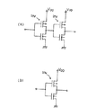
第1バッファ124回路あるいは第2バッファ回路125として、例えば図2(a)に示すような、相補型トランジスタによるインバータInvを2段重ねた回路を用いることができる。また、例えば図2(b)に示す回路を用いることができる。後段のインピーダンスを前段のインピーダンスよりも低くできる回路であれば、広くインピーダンス変換器として使用することができる。
【0051】
インバータを用いる場合には、入出力の信号が反転するため、駆動回路全体としての論理が整合するように、必要に応じて回路に変更を加えなければならない。なお、図1の第1バッファ回路124および第2バッファ回路125の両者にインバータを用いる場合には、他の部分に変更を加えなくても、第1実施形態と同様の動作を確保することができる。
【0052】
上記の構成を有する液晶装置100には、図3に示す表示情報処理回路600からの画像信号がシリアル−パラレルに変換されて出力される。この表示情報処理回路600は、液晶装置100から分離された外付け回路(IC)として設けられていてもよい。この表示情報処理回路600には、一本の画像信号VIDが入力される。そして、表示情報処理回路600は画像信号VIDの画像情報を6つのシリアル−パラレル変換信号に展開し、これらの信号を画像信号VID1〜VID6として出力する。
【0053】
(画素領域の構成)
次に上述の等価回路により構成されたTFTアレイ基板10の画素の構成について、図4を参照して説明する。
【0054】
図4(a)は、データ線、走査線、画素電極が形成されたTFTアレイ基板10の隣接した画素群の平面図である。図4(b)は、図4(a)のC−C’断面図である。
【0055】
図4(a)及び図4(b)において、各画素は、マトリクス状に複数の透明な画素電極9と各画素電極9に接続されたスイッチング素子の一例である画素スイッチング用TFT30とにより構成されている。画素電極9の縦横の境界に各々沿ってデータ線6、走査線3及び容量線3'が設けられており、データ線6を構成する第1導電層は、アルミニウム、クロム等の金属からなり、第1層間絶縁膜4に形成されたコンタクトホール5aを介してTFT30のアモルファスシリコン膜やポリシリコン膜等からなる半導体層1aのうち後述のソース領域1dに電気的接続されている。画素電極9は、第1層間絶縁膜4及び第2層間絶縁膜7に形成されたコンタクトホール8を介して薄膜トランジスタ30の半導体層1aのうち後述のドレイン領域1eに電気的接続されている。また、ゲート絶縁膜2を介して半導体層1aのうちのチャネル形成用領域1a’(図2中右下りの斜線の領域)に対向するように走査線3が配置されている。走査線3を構成する第2導電層はアルミニウム、クロムのような金属で形成する場合もあるが、製造工程において600℃以上の高温にさらされる場合はポリシリコンで形成する場合がある。蓄積容量は、画素スイッチング用TFT30の半導体層1aから延設された第1蓄積容量電極1fを一方の電極とし、ゲート絶縁膜2と同時に形成された絶縁膜を誘電体膜とし、走査線3と同時に形成された容量線3'を他方の電極(第2蓄積容量電極)として構成されている。このような構成を採れば、薄膜で緻密なゲート絶縁膜2を誘電体とすることで、第1蓄積容量電極1fと第2蓄積容量電極3'の重なり面積が小さくても、十分な蓄積容量が得られるため、画素の高開口率化や微細化が容易に実現することができる。
【0056】
画素電極9の上側には、図4(b)に示すようにラビング処理等の所定の配向処理が施された配向膜16が設けられている。画素電極9は例えば、ITO(Indium Tin Oxide)膜などの透明導電性薄膜からなる。また配向膜16は例えば、ポリイミド薄膜などの有機薄膜からなる。
【0057】
他方、対向基板20には、その全面に渡って対向電極21が設けられており、その下側には、ラビング処理等の所定の配向処理が施された配向膜22が設けられている。対向電極21は例えば、ITO膜などの透明導電性薄膜からなる。また配向膜22は、ポリイミド薄膜などの有機薄膜からなる。更に、画素スイッチング用TFT30や液晶のディスクリネーションが発生する領域を覆うように非光透過性の金属膜、金属合金膜、或いは黒色有機膜等により遮光膜23を設けても良い。これにより、コントラスト比の高い画像表示を実現することができる。遮光膜23はTFTアレイ基板10に設けるようにしても良い。このような構成を採れば、TFTアレイ基板10と対向基板20を貼り合わせる際の精度を考慮する必要がないため、透過率のばらつかない液晶装置100を安定して提供することができる。
【0058】
上記の構成を有するTFTアレイ基板10と、対向基板20との間には、電気光学物質としての液晶が封入され、液晶層50が形成される。液晶層50は、画素電極9からの電界が印加されていない状態で配向膜により所定の配向状態を採る。
【0059】
ここで、一般には、半導体層1aのチャネル形成用領域1a’、低濃度ソース領域1b及び低濃度ドレイン領域1c等を形成するアモルファスシリコン膜あるいはポリシリコン膜は、光が入射すると光電変換効果により光電流が発生してしまいTFT30のトランジスタ特性が劣化するが、第1実施形態では、走査線3を上側から覆うようにデータ線6がAl(アルミニウム)等の遮光性の金属薄膜から形成されているので、少なくとも半導体層1aのチャネル形成用領域1a’及びソース側LDD(Lightly Doped Drain)領域1b、ドレイン側LDD領域1cへの投射光(即ち、図3で上側からの光)の入射を効果的に防ぐことが出来る。また、TFT30の下側に、層間絶縁膜を介して、少なくとも半導体層1aのチャネル形成用領域1a’及びLDD領域1b、1cを覆うように遮光膜(図示せず)を設ければ戻り光(即ち、図4(b)で下側からの光)の入射を効果的に防ぐことが出来る。
【0060】
次に、図5を用いてサンプリングスイッチのレイアウトについて説明する。共通にサンプリング制御信号が供給されるサンプリングスイッチ121のブロック毎に第1バッファ回路124と第1バッファ回路124に接続された複数の第2バッファ125が設けられており、第1バッファ回路124と第2バッファ回路125とを接続する6つの分岐配線である第1配線41が第1導電層で形成されている。そして、第1配線41はパラレルに6つに分岐して第2バッファ回路125に接続され、第2バッファ回路125の出力信号(サンプリング制御信号)が、サンプリング制御信号線40を介してサンプリングスイッチ121のゲート電極に入力されるように構成されている。サンプリング制御信号線40は画像信号線に交差する第2配線42と、第2配線42からさらに延長された第3配線43と、サンプリングスイッチのゲート電極となる第4配線48からなる。
【0061】
図5に示されるように、第2バッファ125の出力端子に接続された第2配線42及び第3配線43は、画像信号線115に接続された中継配線80と平行に設けられ、また第2配線42及び第3配線43と中継配線80とは1配線ずつ交互に配置されている。画像信号線115はデータ線6と同様に第1導電層により形成されているため、サンプリング制御信号線40を構成する第2配線42は第1導電層とは別層、例えば走査線3と同様に第2導電層で形成するとよい。またサンプリング制御信号線40のうち画像信号線115に交差しない第3配線43は、上述のように第1導電層及び第2導電層の2層構造にしてコンタクトホール44、45を介して接続すれば、さらに低抵抗化される。
【0062】
サンプリングスイッチ121毎に独立したバッファ回路125を用いているので、サンプリング制御信号線40のインピーダンスを低くすることができる。このため、サンプリングスイッチ121を安定してスイッチングさせることができ、よって表示画像の画質を向上させることができる。
【0063】
次に、第1実施形態の駆動回路の動作について説明する。画像信号VIDは液晶装置100の各画素に対応するデータが時系列的に並んだアナログ信号であり、図3に示すように、表示情報処理回路600はドットクロックDCを基準クロックとして画像信号VIDをサンプリングする。そして、この画像情報を画像信号VIDのサンプリング周期よりも長いデータ長の6本の画像信号VID1〜VID6にシリアル−パラレル変換する。すなわち、表示情報処理回路600は画像信号VIDの画像情報のデータ長を伸張する機能と、シリアルな画像信号VIDをパラレルな信号に変換する機能とを備えるものである。
【0064】
画像信号線115に出力される画像信号VID1〜VID6は、画像信号VIDの連続する6画素分のデータを、順番にドットクロックDCの6周期分のデータ長に伸張したものである。この6画素分の画像信号の先頭はいずれも6画素目のデータの先頭に位置しており、それぞれの画像信号VID1〜VID6は同一のタイミングで出力される。
【0065】
図6では、画像信号VIDの個々の画素データに順番に画素番号(1〜18)を付すとともに、画像信号VID1〜VID6に変換した元の画素データの画像番号を付しており、これにより両者の対応関係を示している。画素番号1〜6の画素データが画像信号VID1〜VID6として出力されるドットクロックDC6周期分の期間では、シフトレジスタ400が出力信号OUT1を出力する。次いで、画素番号7〜12の画素データがVID1〜VID6として出力されるドットクロックDC6周期分の期間では、シフトレジスタ400から出力信号OUT2が出力される。このように、シフトレジスタ400は、新たなシリアル−パラレル変換信号が出力されるドットクロックDC6周期分の期間において、出力信号OUT1,OUT2,OUT3,…を順次出力する。
【0066】
シフトレジスタ400のラッチ回路123aから第1バッファ回路124に出力信号OUT1が出力されると、バッファ回路124の出力が立ち上がり、これによって、第2バッファ回路125は6本のサンプリング制御信号線40に同時にサンプリング制御信号を出力する。6本のサンプリング制御信号線40に供給されるサンプリング制御信号X1〜X6は、6つのサンプリングスイッチ121に供給される。
【0067】
サンプリングスイッチ121に供給されるサンプリング制御信号に応じて、画像信号線115に供給される画像信号VID1〜VID6は、それぞれデータ線6に供給される。例えば第1番目の走査線3と、上記データ線6とに接続された6つの画素のTFT30を介して、画素電極9に書き込みが行われる。このように、6本のデータ線6と、1本の走査線3とによって選択された6つの画素(画素番号1〜6)について、同時に書き込みが行われる。
【0068】
次いで、シフトレジスタ400のラッチ回路123bから第1バッファ回路124bに出力信号OUT2が出力されると、第1バッファ回路124bの出力が立ち上がり、これによって、6つの第2バッファ回路125は6本の相隣接するサンプリング制御信号線40に同時にサンプリング制御信号を出力し、6つのサンプリングスイッチ121をオンさせる。このため、6本のデータ線6と、上記の1本の走査線3とによって選択された次の6つの画素(画素番号7〜12)について、同時に書き込みが行われる。
【0069】
以下同様にして、シフトレジスタ400からの出力信号によって、順次6つずつサンプリングスイッチ121がオンし、6画素ずつの書き込みが実行される。このようにして、第1番目の走査線3の全画素について書き込みを行うことができる。第2番目以降の走査線3のすべてについて順次走査信号を出力しながら上記動作を繰り返すことにより、1フレームの画像が形成される。
【0070】
第1実施形態では、サンプリングスイッチ121のそれぞれに対して第2バッファ回路125を設け、1つの第1バッファ回路124によって6つの第2バッファ回路125を駆動するようにしている。つまり、1つのブロック内のサンプリングスイッチ121はそれぞれ異なる第2バッファ回路125に接続されている。このため、第2バッファ回路125はそれぞれ1つのサンプリングスイッチ121のみを駆動すればよく、その負荷が軽いものとなる。
【0071】
また、同時にサンプリング信号が出力される6本のサンプリング制御信号線40は互いに6つの第2バッファ回路125を介して接続されることになるが、第2バッファ回路125は出力側の信号が入力側にほとんど影響を与えないという性質を有するので、第2バッファ回路125の入力端が出力端の影響を受けて変動することはない。このため、いずれかのサンプリング制御信号線40の信号は、第2バッファ回路125の入力側の電圧にほとんど影響を与えることはない。なお、第2バッファ回路125の入力側には第1バッファ回路124の出力端が接続されており、そのインピーダンスは低くされているから、なおさら第2バッファ回路125の入力端の電圧は変動しにくい。
【0072】
このため、例えばサンプリング制御信号線40に何らかの原因でノイズが混入しても、そのノイズの影響を受けて第2バッファ回路125の入力側の電圧が変動し、これによりサンプリング制御信号線40の全体が第2バッファ回路125によって駆動され揺さぶられるということはない。同様に、サンプリング制御信号線40のいずれかにノイズが混入したとしても、これによって他のサンプリング制御信号線が第2バッファ回路125によって揺さぶられることはない。
【0073】
また、第2バッファ回路125の出力側は低インピーダンスとされているから、画像信号線115から供給される画像信号VID1〜VID6やデータ線6に供給されるデータ信号S1、S2…、あるいは各部のノイズ等が、容量結合を介して直接サンプリング制御信号線40に入るということもほとんどない。
【0074】
このように、第1実施形態では、各サンプリング制御信号線40毎に第2バッファ回路125を設けているので、各種ノイズがサンプリング制御信号線40に混入しにくく、サンプリング信号の純度を高く維持することができる。このため、第1実施形態の駆動回路によれば、ゴースト等が発生せず、良好な表示画像を得ることができるものである。
【0075】
本発明による駆動回路は、従来の駆動回路におけるゴースト現象の発生原因の解析に基づいて、発明されたものである。以下、本発明による駆動回路の作用効果を明らかにするため、図13を用いて従来の駆動回路におけるゴースト発生の機構等について説明する。
【0076】
図13の駆動回路では、6つのサンプリングスイッチ121からなるブロック毎に、同時にサンプリング制御信号が供給される6本のサンプリング制御信号線40は共通に1つのバッファ回路124に接続されている。一方、1つのブロック内のサンプリング制御信号線40と画像信号線115、およびサンプリング制御信号線40、データ線6は、それぞれサンプリングスイッチ121に形成される容量(例えばサンプリングスイッチ121として電界効果トランジスタを用いる場合には、そのゲート・ソース間容量、ゲート・ドレイン間容量等)を介して結合された状態にある。
【0077】
このため、例えば、サンプリングスイッチ121のオンに伴ってデータ線6の電圧が急激に変動すると、その変動に見合った成分(微分波形)が上記容量を介してサンプリング制御信号線40に回り込みノイズとなる。ところが、1つのブロック内のサンプリング制御信号線40は共通に接続されているので、例えば1つのサンプリング制御信号線40に侵入したノイズは、さらにブロック内の他のサンプリング制御信号線40にも容易に伝播する。上記のように、サンプリングスイッチ121が同時にオンしたときにサンプリング制御信号線40に現れるノイズはデータ線6の変動幅に依存し、その変動幅はそのときの画像信号(電圧値)に依存するから、結局サンプリング制御信号線40に重畳されるノイズ成分は画像信号の電圧値と相関があることになる。
【0078】
このような現象は、サンプリング制御信号線40のいずれかから他のサンプリング制御信号線への影響についてもそのまま当てはまる。したがって、サンプリング制御信号線40の電圧は、画素電極9への書き込み時における画像信号線115の電圧に応じて変動し、しかもサンプリング制御信号線40の変動は互いに同期したものとなることが判る。
【0079】
そしてサンプリング制御信号線40の電圧変動は、ブロック内のサンプリングスイッチ121を介してデータ線6の電圧を変動させる。例えば、サンプリングスイッチ121として電界効果トランジスタ等を用いる場合には、サンプリング制御信号線40に接続されたゲート電圧の変動にともなって、その素子の特性に従いドレイン電圧が変動するので、データ線6の電圧がすべて変動する。
【0080】
このように、サンプリング制御信号線40の電圧は、画素電極9への書き込み時における画像信号線115全体の電圧の影響を受けて変化し、その変化がデータ線6全体の電圧を変動させる。すなわち、データ線6はサンプリングスイッチ121によって直接接続されることのない、他の画像信号線の電圧値の影響を受けて変動するので、画像にゴーストを生じさせることになる。
【0081】
また、例えばサンプリング制御信号線40は共通のバッファ回路124に接続されているので、第1実施形態におけるサンプリング制御信号線40とは異なり、引き回しが長くならざるを得ない。このため、サンプリング制御信号線40はサンプリングスイッチ121の近くでインピーダンスが上昇しやすく、比較的ノイズの飛びつきが多くなる。このため、上記のようなゴーストがより発生しやすい状況となる。
【0082】
このように従来の駆動回路では、データ線6の電圧が本来そのデータ線6とは無関係の画像信号の影響を受けて変動し、また、サンプリング制御信号線40に比較的ノイズが乗りやすいため、ゴーストの全くない、良好な画像を得ることは困難である。
【0083】
これに対して、第1実施形態の駆動回路では、各サンプリングスイッチ121毎に第2バッファ回路125を用意し、第2バッファ回路125を介してサンプリングスイッチ121をスイッチングしている。このため、異なるサンプリング制御信号線40の間には必ず第2バッファ125が挿入されることとなり、異なるサンプリング制御信号線40間の結合をほぼ完全に遮断することができる。
【0084】
すなわち、第1の実施の形態の駆動回路では、例えば1つのサンプリング制御信号線40にノイズが侵入したとしても、そのノイズは別のサンプリング制御信号線40には伝播しないので、データ線6の電圧が変動することはない。
【0085】
また、サンプリング制御信号線40の各々に第2バッファ125の出力端が接続されているので、サンプリング制御信号線40の配線の引き回しを短くすることができ、そのインピーダンスの上昇が抑えられる。このため、サンプリング制御信号線40にノイズが飛びつきにくい。
【0086】
したがって、第1の実施の形態の駆動回路では、従来の駆動装置に見られるようなゴーストが発生せず、良好な表示画像を得ることができる。
【0087】
−第2実施形態−
以下、図7を用いて、本発明による電気光学装置の駆動回路の第2実施形態について説明する。第2実施形態では、サンプリング制御信号のパルスの形状を第1実施形態と異なるものとしている。なお、第1実施形態と同一の構成要素についてはその説明を省略する。
【0088】
第1実施形態では、サンプリング制御信号のパルス幅はシリアル−パラレル変換信号と同一のパルス幅(ドットクロックDC6周期分)に設定されている(図2)が、第2実施形態では、図6に示すようにサンプリング制御信号線40に出力されるサンプリング信号のパルス幅を、画像信号線115の画像信号VID1〜VID6のパルス幅よりも小さくして、サンプリング制御信号X1〜X6、X7〜X12、X13〜X18、…のパルスを画像信号の立ち上がりと立ち下がりの間に位置させている。
【0089】
このように、サンプリング信号のパルスを画像信号の立ち上がりおよび立ち下がりに重ならない期間に設定すれば、画像信号が安定している期間に書き込みを実行できる。したがって、高精度の信号をデータ線6に供給することができ、より一層良好な画像を得ることができる。
【0090】
なお、図7ではサンプリング制御信号のパルス幅をドットクロックDC4周期分の幅としているが、サンプリング制御信号のパルス幅は液晶層50に対する書き込みが可能な範囲で適宜選択することができる。
【0091】
−第3実施形態−
以下、図8を用いて本発明による電気光学装置の駆動回路の第3実施形態について説明する。図8は第3実施形態の等価回路図である。なお、第1実施形態と同一の構成要素については、同一符号を付してその説明を省略する。
【0092】
第3実施形態では、図8に示すように、シフトレジスタ400の出力端にそれぞれ接続された各第1バッファ回路124の出力端には、それぞれ3つの第2バッファ回路125が接続されている。また、各第2バッファ回路125には、それぞれ2つのサンプリングスイッチ121が接続されている。
【0093】
次に図9を用いて第3実施形態のレイアウトについて説明する。
【0094】
サンプリング制御信号線121は、第2バッファ125回路の出力端子からサンプリングスイッチ121に向けて、中継配線80と平行に交差された第2配線42と、第2配線42に接続されてさらに延設された第3配線43と、画像信号線115と平行に延設された接続配線45と、各サンプリングスイッチ121の各ゲート電極から引き出され、接続配線45と接続された第4配線48とからなる。第2配線42と第2配線に接続された第3配線43の間隙には2本の中継配線80が第2配線42及び第3配線43に平行に延設されている。さらに、第3配線43はコンタクトホール47を介して接続配線46に接続され、接続配線46は中継配線80に交差するように延設されている。また、第3配線43はコンタクトホール44と45の間は第1導電層と第2導電層の二重配線となっている。接続配線45は第1導電層からなり、サンプリングスイッチ121に接続されるように櫛型に延長された第4配線48とコンタクトホール47を介して接続されている。
【0095】
第3実施形態では、隣り合った2つのサンプリングスイッチ121に入力される2つのサンプリング制御信号線40が互いに共通に第2バッファ回路125に接続されている。従って、図13に示す従来の駆動回路と比較すればバッファ回路125の負荷が軽いため、バッファ回路125の出力側にはノイズが混入しにくく、したがって、サンプリング制御信号の変動を良好に抑制することができる。このため、データ線の信号の精度を高めることができ、よって良好が画像を得ることができる。
【0096】
また、2つ以上離れたデータ線6間への影響はバッファ回路125によって排除されるため、画面上で像が二重に表示されているようには認識し難く、事実上、ゴーストを排除することができる。
【0097】
第3実施形態では、1つの第2バッファ回路125から2つのサンプリングスイッチにサンプリング制御信号を供給するようにしているが、1つのバッファ回路から3つ以上のサンプリングスイッチにサンプリング制御信号を供給するようにしてもよい。
【0098】
−第4実施形態−
以下、図10を用いて本発明による電気光学装置の駆動回路の第4実施形態について説明する。図10は第4実施形態の等価回路図である。なお、第1実施形態と同一の構成要素については、同一符号を付してその説明を省略する。
【0099】
第4実施形態では、図10に示すように、第1バッファ回路124と第2バッファ回路125とを互いに画像信号線115を隔てて配置し、第1バッファ回路124からの出力線である第1配線を第2バッファ回路125の側で分岐させている。つまり、第1バッファ回路に接続された第1配線は画像信号線115と交差するように延設し、交差した後に分岐して複数の第2バッファ回路に並列に接続されている。
【0100】
このようなレイアウトを採用することにより、第4実施形態では第2バッファ125の出力線に該当するサンプリング制御信号線40の配線の引き回しをより一層短くすることができ、また、画像信号線115からサンプリング制御信号線40へのノイズの飛びつきを避けることができる。尚、実施形態1で説明したように、本実施形態においても第1バッファ回路124を設けなくても、シトレジスタ400に大2バッファ回路125を直接駆動できる能力がある場合には、第1バッファ回路124を取り除き、シフトレジスタ400の出力端を直接第2バッファ回路125に接続するようにしても良い。
【0101】
(液晶表示装置の全体レイアウト)
以下、図11および図12を用いて、本発明が適用されるアクティブマトリクス型の液晶表示装置の全体レイアウトについて第1の実施の形態の場合を例に挙げて説明する。
【0102】
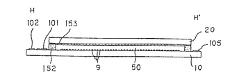
図11において、TFTアレイ基板10の上には、シール材152がその縁に沿って設けられており、その内側に並行して、額縁としての遮光膜153が設けられている。シール材152の外側の領域には、データ線駆動回路101及び実装端子102がTFTアレイ基板10の一辺に沿って設けられており、走査線駆動回路104が、この一辺に隣接する2辺に沿って設けられている。シフトレジスタ400、第1及び第2バッファ回路124,125はデータ線駆動回路101に含まれる。走査線駆動回路104に供給される走査信号遅延が問題にならないのならば、図1に示すように走査線駆動回路104は片側だけでも良いことは言うまでもない。また、データ線駆動回路101を画像表示領域の辺に沿って両側に配列してもよい。例えば奇数列のデータ線は画像表示領域DAの一方の辺に沿って配設されたデータ線駆動回路から画像信号を供給し、偶数列のデータラインは画像表示領域DAの反対側の辺に沿って配設されたデータ線駆動回路から画像信号を供給するようにしてもよい。この様にデータ線を櫛歯状に駆動するようにすれば、データ線駆動回路の占有面積を拡張することができるため、複雑な回路を構成することが可能となる。更にTFTアレイ基板10の残る一辺には、画像表示領域DAの両側に設けられた走査線駆動回路104間をつなぐための複数の配線105が設けられており、更に、額縁としての遮光膜153の下に隠れてサンプリング回路121を設けるようにすると、データ線駆動回路101のレイアウト領域を拡張することができるため、大規模回路の内蔵や液晶装置100の小型化が実現できる。また、対向基板20のコーナー部の少なくとも1箇所においては、TFTアレイ基板10と対向基板20との間で電気的導通をとるための導通材106が設けられている。そして、図12に示すように、図11に示したシール材152とほぼ同じ輪郭を持つ対向基板20が当該シール材152によりTFTアレイ基板10に固着され、内部に液晶50が封入される。
【0103】
以上、図1〜図12を参照して説明した各実施の形態における液晶装置のTFTアレイ基板10上には更に、製造途中や出荷時の当該液晶装置の品質、欠陥等を検査するための検査回路等を形成してもよい。また、データ線駆動回路101及び走査線駆動回路104をTFTアレイ基板10の上に設ける代わりに、例えばTAB(テープオートメイテッドボンディング基板)上に実装された駆動用LSIに、TFTアレイ基板10の周辺部に設けられた異方性導電フィルムを介して電気的及び機械的に接続するようにしてもよい。また、対向基板20の投射光が入射する側及びTFTアレイ基板10の出射光が出射する側には各々、例えば、TN(ツイステッドネマティック)モード、STN(スーパーTN)モード、D−STN(ダブル−STN)モード等の動作モードや、ノーマリーホワイトモード/ノーマリーブラックモードの別に応じて、偏光フィルム、位相差フィルム、偏光板などが所定の方向で配置される。
【0104】
上記実施の形態では、TFTを用いて各画素を駆動してもよいし、あるいはTFT以外の、例えばTFD(薄膜ダイオード)等のアクティブ素子を用いることも可能であり、さらに液晶装置をパッシブマトリクス型の液晶装置として構成することも可能である。また、シリコン基板にスイッチング素子を形成してなる表示装置の駆動回路にも適用可能である。さらに、本発明は液晶装置以外の電気光学装置についても、広く適用することができる。
【0105】
(電子機器)
次に、以上詳細に説明した電気光学装置の一例として液晶装置100を備えた電子機器の実施の形態について図14から図16を参照して説明する。
【0106】
先ず図14に、このように液晶装置100を備えた電子機器の概略構成を示す。
【0107】
図14において、電子機器は、表示情報出力源1000、表示情報処理回路1002、駆動回路1004、液晶装置100、クロック発生回路1008並びに電源回路1010を備えて構成されている。表示情報出力源1000は、ROM(Read Only Memory)、RAM(Random Access Memory)、光ディスク装置などのメモリ、画像信号を同調して出力する同調回路等を含み、クロック発生回路1008からのクロック信号に基づいて、所定フォーマットの画像信号などの表示情報を表示情報処理回路1002に出力する。表示情報処理回路1002は、増幅・極性反転回路、シリアル−パラレル変換回路、ローテーション回路、ガンマ補正回路、クランプ回路等の周知の各種処理回路を含んで構成されており、クロック信号に基づいて入力された表示情報からデジタル信号を順次生成し、クロック信号CLKと共に駆動回路1004に出力する。駆動回路1004は、液晶装置100を駆動する。電源回路1010は、上述の各回路に所定電源を供給する。尚、液晶装置100を構成する液晶装置用基板の上に、駆動回路1004を搭載してもよく、これに加えて表示情報処理回路1002を搭載してもよい。
【0108】
次に図15から図16に、このように構成された電子機器の具体例を各々示す。
【0109】
図15において、電子機器の一例たる液晶プロジェクタ1100は、上述した駆動回路1004が液晶装置用基板上に搭載された液晶装置100を含む液晶表示モジュールを3個用意し、各々RGB用のライトバルブ100R、100G及び100Bとして用いたプロジェクタとして構成されている。液晶プロジェクタ1100では、メタルハライドランプ等の白色光源のランプユニット1102から投射光が発せられると、3枚のミラー1106及び2枚のダイクロイックミラー1108によって、RGBの3原色に対応する光成分R、G、Bに分けられ、各色に対応するライトバルブ100R、100G及び100Bに各々導かれる。この際特にB光は、長い光路による光損失を防ぐために、入射レンズ1122、リレーレンズ1123及び出射レンズ1124からなるリレーレンズ系1121を介して導かれる。そして、ライトバルブ100R、100G及び100Bにより各々変調された3原色に対応する光成分は、ダイクロイックプリズム1112により再度合成された後、投射レンズ1114を介してスクリーン1120にカラー画像として投射される。
【0110】
図16において、電子機器の他の例たるマルチメディア対応のラップトップ型のパーソナルコンピュータ(PC)1200は、上述した液晶装置100がトップカバーケース内に設けられており、更にCPU、メモリ、モデム等を収容すると共にキーボード1202が組み込まれた本体1204を備えている。
【0111】
以上図15から図16を参照して説明した電子機器の他にも、液晶テレビ、ビューファインダ型又はモニタ直視型のビデオテープレコーダ、カーナビゲーション装置、電子手帳、電卓、ワードプロセッサ、エンジニアリング・ワークステーション(EWS)、携帯電話、テレビ電話、POS端末、タッチパネルを備えた装置等などが図14に示した電子機器の例として挙げられる。
【0112】
以上説明したように、本実施の形態によれば、製造効率が高く高品位の画像表示が可能な液晶装置を備えた各種の電子機器を実現できる。
【0113】
【発明の効果】
以上に説明したように、本発明によれば前記シフトレジスタの出力端に接続された第1バッファ回路と、前記第1バッファ回路の出力端に各々接続された複数の第2バッファ回路とを有し、前記複数の第2バッファ回路の出力端は前記ブロック内のサンプリングスイッチに接続されているので、サンプリング制御信号の波形の乱れを良好に抑制できるとともに、サンプリング制御信号線を介してのノイズの侵入を防ぐことができる。したがってゴーストの極めて少ない、あるいはゴーストのない、良好な画像を得ることができる。
【図面の簡単な説明】
【図1】第1実施形態の電気光学装置の駆動回路を示す等価回路図。
【図2】インピーダンス変換器の回路を示す図であり、(a)はバッファ回路を示す等価回路図、(b)はインバータの回路を示す等価回路図。
【図3】表示情報処理回路および液晶装置の接続関係を示す図。
【図4】本発明の第1実施形態の画素群の平面図であり、(b)は図4(a)のC−C’断面図。
【図5】第1実施形態の駆動回路のレイアウトを示す図。
【図6】第1実施形態の電気光学装置の駆動回路の動作を示すタイミングチャート。
【図7】第2実施形態の電気光学装置の駆動回路の動作を示すタイミングチャート。
【図8】第3実施形態の駆動回路の等価回路図。
【図9】第3実施形態の電気光学装置の駆動回路のレイアウト図。
【図10】第4実施形態の電気光学装置の等価回路図。
【図11】電気光学装置全体構成を示す平面図。
【図12】図10のH−H’線における断面図。
【図13】従来の電気光学装置の駆動回路を示す等価回路図。
【図14】本発明による電子機器の実施の形態の概略構成を示すブロック図である。
【図15】電子機器の一例として液晶プロジェクタを示す断面図である。
【図16】電子機器の他の例としてパーソナルコンピュータを示す正面図である。
【符号の説明】
100 液晶装置
101 走査線駆動回路
121 サンプリングスイッチ
400 シフトレジスタ
124 第1バッファ回路
125 第2バッファ回路
115 画像信号線[0001]
BACKGROUND OF THE INVENTION
The present invention relates to a configuration of a drive circuit used in an active matrix type electro-optical device or the like. More specifically, the present invention relates to an electro-optical device drive circuit and an electro-optical device that simultaneously sample image signals from a plurality of image signal lines and write simultaneously to a plurality of data lines.
[0002]
[Prior art]
For example, in an active matrix liquid crystal device as an example of an electro-optical device, a switching element and a switching element including a plurality of scanning lines, a plurality of data lines, a thin film transistor connected to each scanning line and each data line, and the like. A pixel composed of connected pixel electrodes. The operation of writing an image signal in the liquid crystal layer of each pixel is performed by dot sequential driving through switching elements such as thin film transistors connected to a plurality of scanning lines.
[0003]
In such an active matrix liquid crystal device, it is necessary to sample the image signal by sequentially switching the sampling switch provided for each data line at the speed of the dot sequential drive for the above-described dot sequential drive. At this time, there arises a problem that the switching characteristic of the sampling switch cannot sufficiently follow the frequency of the input image signal. In general, in the case of a display device with a built-in driver in which a driver circuit is formed at the same time as a pixel, the driving capability of a sampling thin film transistor is lower than in the case of a display device using an external driver, and the problem becomes more remarkable. Further, in the case of a high-definition display device having a large number of pixels, the above problem becomes more noticeable because the frequency of the input image signal becomes high.
[0004]
For this reason, as in the liquid crystal device shown in FIG. 13, the image signal is converted into, for example, six serial-parallel signals, the data length per pixel is lengthened, and the signal frequency input to the liquid crystal device is lowered. Is disclosed. By this serial-parallel conversion, for example, even if the frequency characteristics of a thin film transistor as a sampling switch are not sufficient, the data length per pixel can be increased and the resolution can be increased.
[0005]
In the liquid crystal device of FIG. 13, six
[0006]
[Problems to be solved by the invention]
However, when the configuration of FIG. 13 is adopted, there is a problem that ghost is likely to occur in the image of the liquid crystal device. In general, the coupling structure between the sampling switch and the data line has poor frequency characteristics. In addition, the phase of the sampling control signal that controls the sampling switch varies. For these reasons, the image signal to be originally written is written not only to the block but also to a pixel one block ahead, and a ghost is generated. In other words, since there are a large number of sampling switches to which the sampling control signal is supplied at the same time, it must be sampled at that time, but it will be sampled at a time deviated from that, causing a ghost. It is. In particular, if the number of sampling switches that are driven simultaneously increases by 6, 12, 24, or the like, the influence on the entire simultaneously driven block also increases.
[0007]
SUMMARY An advantage of some aspects of the invention is that it provides a drive circuit for an electro-optical device capable of obtaining a good display image without occurrence of a ghost or the like.
[0008]
[Means for Solving the Problems]
In order to solve the above problems, a drive circuit for an electro-optical device according to the present invention includes a plurality of data lines, a plurality of scanning lines, the switching lines connected to the data lines and the scanning lines, and the switching elements. A plurality of image signal lines for supplying an image signal, and sampling each of the image signals supplied to the plurality of image signal lines to each of the data A plurality of sampling switches to be supplied to the line, a shift register that outputs a transfer signal in common to each block composed of a plurality of sampling switches, a first buffer circuit connected to an output terminal of the shift register, and each of the first A plurality of second buffer circuits connected in parallel to the output terminal of the buffer circuit, each of the output terminals of the plurality of second buffer circuits being in the block Characterized by comprising connected to the sampling switch.
[0009]
According to the drive circuit of the electro-optical device of the present invention, the sampling control signal means includes a first buffer circuit provided in common for each block, and a plurality of second buffer circuits connected to each first buffer circuit. The outputs of the plurality of second buffer circuits are supplied to the plurality of sampling switches in the block.
[0010]
Therefore, in the case where the sampling switch is driven via a buffer circuit that is divided and connected to several sampling switches in the block, compared to the case where the buffer circuit is simply connected in common to each sampling switch block. Since the load is reduced, it is difficult for noise to be mixed into the output side of the buffer circuit, and the disturbance of the waveform of the sampling signal supplied to the sampling switch can be suppressed. For this reason, it is possible to effectively suppress the voltage fluctuation of the data line due to the disturbance of the waveform of the sampling control signal, and it is possible to realize an electro-optical device that does not cause image quality deterioration such as a ghost.
[0011]
Further, since the sampling switches to which the sampling control signal is commonly supplied are connected to the output terminals of the different buffer circuits, propagation of the sampling control signal between the different sampling switches can be greatly reduced. For this reason, even if noise is mixed in the sampling control signal when the sampling switch is turned on due to, for example, the capacitance formed in the sampling switch, the noise propagates to the sampling control signal of other sampling switches Is effectively prevented. Therefore, an image with very little ghost or no ghost can be displayed on the electro-optical device.
[0012]
The drive circuit of the electro-optical device according to the present invention is characterized in that each of the plurality of sampling switches in one block is connected to a different second buffer circuit.
[0013]
According to this aspect, the sampling control signal is input to each sampling switch via the second buffer circuit provided independently for each sampling switch. For this reason, since the load when driving the sampling switch becomes extremely light, it becomes difficult for noise to be mixed into the output side of the second buffer circuit, and the disturbance of the waveform of the sampling control signal can be remarkably suppressed. Therefore, the electro-optical device can be driven with high accuracy.
[0014]
Further, since the sampling control signals for supplying the sampling control signals to the respective sampling switches are connected to the output terminals of the different second buffer circuits, the signal propagation between the sampling control signals of the different sampling switches is greatly reduced. Or the propagation of such signals can be extinguished. For this reason, even if noise is mixed between the sampling control signal lines, the noise is effectively prevented from propagating to the sampling control signal lines of other sampling switches. Therefore, an image with very little ghost or no ghost can be displayed on the electro-optical device.
[0015]
One aspect of the drive circuit of the electro-optical device according to the present invention is characterized in that a plurality of sampling switches in one block are connected to one second buffer circuit.
[0016]
According to this aspect, since a plurality of sampling switches are connected to one second buffer circuit, it is possible to prevent the total number of second buffer circuits from being increased unnecessarily, and space can be used effectively.
[0017]
In one aspect of the drive circuit of the electro-optical device according to the present invention, an inverter is used as the impedance converter.
[0018]
According to this aspect, since the impedance on the output side of the inverter can be lowered, it becomes difficult for noise to be mixed into the sampling control signal line, and the disturbance of the waveform of the sampling control signal line supplied to each element is effectively prevented. Can be suppressed.
[0019]
In two aspects of the driving circuit of the electro-optical device according to the present invention, the plurality of data lines, the plurality of scanning lines, the switching elements connected to the data lines and the scanning lines, and the switching elements are connected A drive circuit for an electro-optical device having a pixel electrode, which samples a plurality of image signal lines for supplying image signals and an image signal supplied to the plurality of image signal lines and supplies the sampled data signals to the data lines. A plurality of sampling switches; a shift register that outputs a transfer signal in common to each block composed of a plurality of sampling switches; and a plurality of buffer circuits connected in parallel to an output terminal of the shift register. Each of the output ends of the buffer circuit is connected to a sampling switch in the block.
[0020]
According to this aspect of the present invention, the buffer circuit is divided and connected to several sampling switches in the block as compared with the case where the buffer circuit is simply connected to each sampling switch block. Since the load when driving the sampling switch is reduced, it is difficult for noise to be mixed into the output side of the buffer circuit, and the disturbance of the waveform of the sampling signal supplied to the sampling switch can be suppressed. For this reason, it is possible to effectively suppress the voltage fluctuation of the data line due to the disturbance of the waveform of the sampling control signal, and it is possible to realize an electro-optical device that does not cause image quality deterioration such as a ghost.
[0021]
Further, since the sampling switches to which the sampling control signal is commonly supplied are connected to the output terminals of the different buffer circuits, propagation of the sampling control signal between the different sampling switches can be greatly reduced. For this reason, even if noise is mixed in the sampling control signal when the sampling switch is turned on due to, for example, the capacitance formed in the sampling switch, the noise propagates to the sampling control signal of other sampling switches Is effectively prevented. Therefore, an image with very little ghost or no ghost can be displayed on the electro-optical device.
[0022]
The drive circuit of the electro-optical device of the present invention includes a plurality of data lines, a plurality of scanning lines, the data lines, switching elements connected to the scanning lines, and pixel electrodes connected to the switching elements. A plurality of image signal lines that supply image signals, and a sampling switch that samples the image signals supplied to the plurality of image signal lines and supplies the image signals to the data lines. A relay wiring for connecting the image signal line and the sampling switch, a shift register for outputting a transfer signal in common to each block composed of a plurality of sampling switches, and a first buffer connected to an output terminal of the shift register Circuit, and a plurality of second buffer circuits connected in parallel to the output ends of the first buffer circuits, and the plurality of second buffers Sampling control signal line that connects the sampling switch and road is characterized by comprising cross the image signal line along the gap of the relay wiring.
[0023]
According to this aspect of the present invention, the buffer circuit is divided and connected to several sampling switches in the block as compared with the case where the buffer circuit is simply connected to each sampling switch block. Since the load when driving the sampling switch is reduced, it is difficult for noise to be mixed into the output side of the buffer circuit, and the disturbance of the waveform of the sampling signal supplied to the sampling switch can be suppressed. For this reason, it is possible to effectively suppress the voltage fluctuation of the data line due to the disturbance of the waveform of the sampling control signal, and it is possible to realize an electro-optical device that does not cause image quality deterioration such as a ghost.
[0024]
Further, since the sampling switches to which the sampling control signal is commonly supplied are connected to the output terminals of the different buffer circuits, propagation of the sampling control signal between the different sampling switches can be greatly reduced. For this reason, even if noise is mixed in the sampling control signal when the sampling switch is turned on due to, for example, the capacitance formed in the sampling switch, the noise propagates to the sampling control signal of other sampling switches Is effectively prevented. Therefore, an image with very little ghost or no ghost can be displayed on the electro-optical device.
[0025]
The drive circuit of the electro-optical device of the present invention includes a plurality of data lines, a plurality of scanning lines, a switching element electrically connected to the data lines and the scanning line, and electrically connected to the switching element. A plurality of image signal lines for supplying image signals, and image signals supplied to the plurality of image signal lines for sampling the plurality of data lines. Each block comprising a plurality of sampling switches supplied to each, a relay wiring connecting the image signal line and the sampling switch, and n (n is an integer of 2 or more) sampling switches among the plurality of sampling switches A shift register that outputs a transfer signal in common, and a first buffer circuit that receives the transfer signal from an output terminal of the shift register; A plurality of second buffer circuits connected in parallel to the output terminals of the first buffer circuits, and an output line connecting the first buffer circuit and the second buffer circuit intersects the image signal line. Then, the sampling control signal is branched and connected in parallel to the plurality of second buffer circuits, and the sampling control signal supplied from each of the second buffer circuits is sampled via the sampling control signal line connected to the second buffer circuit. It is supplied to the gate of the switch.
[0026]
According to this aspect of the present invention, since the output line connecting the first buffer circuit and the second buffer circuit intersects the image signal line, and the second buffer circuit is provided after the intersection, the sampling control signal is The influence by the image signal can be suppressed, and the wiring can be further shortened.
In the drive circuit of the electro-optical device according to the aspect of the invention, the gates of the n sampling switches in one block are connected to different second buffer circuits.
[0027]
According to this aspect, the sampling control signal is input to each sampling switch via the second buffer circuit provided independently for each sampling switch. For this reason, since the load when driving the sampling switch becomes extremely light, it becomes difficult for noise to be mixed into the output side of the second buffer circuit, and the disturbance of the waveform of the sampling control signal can be remarkably suppressed. Therefore, the electro-optical device can be driven with high accuracy.
[0028]
Further, since the sampling control signals for supplying the sampling control signals to the respective sampling switches are connected to the output terminals of the different second buffer circuits, the signal propagation between the sampling control signals of the different sampling switches is greatly reduced. Or the propagation of such signals can be extinguished. For this reason, even if noise is mixed between the sampling control signal lines, the noise is effectively prevented from propagating to the sampling control signal lines of other sampling switches. Therefore, an image with very little ghost or no ghost can be displayed on the electro-optical device.
[0029]
In the drive circuit of the electro-optical device according to the aspect of the invention, the gates of the plurality of sampling switches in the block are connected to one second buffer circuit.
[0030]
According to this aspect, since a plurality of sampling switches are connected to one second buffer circuit, it is possible to prevent the total number of second buffer circuits from being increased unnecessarily, and space can be used effectively.
[0031]
The drive circuit of the electro-optical device of the present invention includes a plurality of data lines, a plurality of scanning lines, the data lines, switching elements connected to the scanning lines, and pixel electrodes connected to the switching elements. A plurality of image signal lines for supplying image signals and a plurality of samplings for sampling the image signals supplied to the plurality of image signal lines and supplying the image signals to the data lines A shift register that outputs a transfer signal in common to each block including a plurality of sampling switches, and a buffer circuit connected in parallel to the output end of the shift register, and the output end of the shift register and the An output line connecting the buffer circuit crosses the image signal line and then branches into a plurality of branches and is connected in parallel to the plurality of buffer circuits. Characterized by a sampling control signal supplied from the buffer circuit via a sampling control signal lines supplied to the sampling switch.
[0032]
According to this aspect of the present invention, since the output line connecting the output terminal of the shift register and the buffer circuit intersects the image signal line, and the buffer circuit is provided after the intersection, the image signal to the sampling control signal is provided. The influence of the noise can be suppressed, and the wiring can be further shortened.
[0033]
DETAILED DESCRIPTION OF THE INVENTION
-First embodiment-
A first embodiment in which the drive circuit of the electro-optical device according to the present invention is applied to an active matrix liquid crystal device will be described below with reference to FIGS.
[0034]
FIG. 1 is an equivalent circuit of various elements, wirings, and the like in a plurality of pixels formed in a matrix that forms an image display area of a liquid crystal device.
[0035]
In FIG. 1, a plurality of pixels formed in a matrix that form the image display region 110 a of the liquid crystal device according to the present embodiment includes, for example, a thin film transistor (hereinafter, referred to as a switching element for controlling the
[0036]
Particularly in the present embodiment, the image signals S1, S2,..., Sn written to the
[0037]
Further, the
[0038]
Next, the drive circuit of the liquid crystal device of this embodiment will be described. In addition to the image display area 110a provided with scanning lines, data lines, etc. as described above, the data
[0039]
The scanning
[0040]
The data line driving
[0041]
Next, a more detailed configuration of the data line driving
[0042]
The data line driving
[0043]
As described above, the transfer signals OUT1, OUT2,..., OUTn from the
Next, specific configurations of the
[0044]
As shown in FIG. 1, each
[0045]
The output terminal of the first
[0046]
Each of the sampling switches 121 can be configured by a semiconductor element such as a field effect transistor. When, for example, a field effect transistor is used as the
[0047]
The
[0048]
The
[0049]
The
[0050]
As the
[0051]
When an inverter is used, since the input / output signals are inverted, the circuit must be changed as necessary so that the logic of the entire drive circuit is matched. In the case where inverters are used for both the
[0052]
In the
[0053]
(Configuration of pixel area)
Next, the configuration of the pixel of the
[0054]
FIG. 4A is a plan view of adjacent pixel groups on the
[0055]
4A and 4B, each pixel includes a plurality of
[0056]
On the upper side of the
[0057]
On the other hand, a counter electrode 21 is provided over the entire surface of the
[0058]
Between the
[0059]
Here, in general, an amorphous silicon film or a polysilicon film that forms the
[0060]
Next, the layout of the sampling switch will be described with reference to FIG. A plurality of
[0061]
As shown in FIG. 5, the
[0062]
Since an
[0063]
Next, the operation of the drive circuit of the first embodiment will be described. The image signal VID is an analog signal in which data corresponding to each pixel of the
[0064]
The image signals VID1 to VID6 output to the
[0065]
In FIG. 6, pixel numbers (1 to 18) are sequentially assigned to individual pixel data of the image signal VID, and image numbers of the original pixel data converted into the image signals VID1 to VID6 are added. The correspondence relationship is shown. The
[0066]
When the output signal OUT1 is output from the
[0067]
In response to the sampling control signal supplied to the
[0068]
Next, when the output signal OUT2 is output from the
[0069]
Similarly, in accordance with the output signal from the
[0070]
In the first embodiment, the
[0071]
In addition, the six sampling
[0072]
Therefore, for example, even if noise is mixed into the sampling
[0073]
Further, since the output side of the
[0074]
Thus, in the first embodiment, since the
[0075]
The drive circuit according to the present invention has been invented based on the analysis of the cause of occurrence of the ghost phenomenon in the conventional drive circuit. Hereinafter, in order to clarify the operation and effect of the drive circuit according to the present invention, a ghost generation mechanism and the like in the conventional drive circuit will be described with reference to FIG.
[0076]
In the drive circuit of FIG. 13, six sampling
[0077]
For this reason, for example, when the voltage of the
[0078]
Such a phenomenon also applies to the influence of any one of the sampling
[0079]
The voltage variation of the sampling
[0080]
Thus, the voltage of the sampling
[0081]
Further, for example, since the sampling
[0082]
As described above, in the conventional driving circuit, the voltage of the
[0083]
On the other hand, in the drive circuit of the first embodiment, the
[0084]
That is, in the driving circuit according to the first embodiment, even if noise enters one sampling
[0085]
In addition, since the output terminal of the
[0086]
Therefore, the drive circuit of the first embodiment does not generate a ghost as seen in a conventional drive device, and a good display image can be obtained.
[0087]
-Second Embodiment-
Hereinafter, a second embodiment of the drive circuit of the electro-optical device according to the present invention will be described with reference to FIG. In the second embodiment, the pulse shape of the sampling control signal is different from that of the first embodiment. Note that the description of the same components as those in the first embodiment is omitted.
[0088]
In the first embodiment, the pulse width of the sampling control signal is set to the same pulse width as that of the serial-parallel conversion signal (for 6 periods of the dot clock DC) (FIG. 2). In the second embodiment, FIG. As shown, the pulse width of the sampling signal output to the sampling
[0089]
In this way, if the sampling signal pulse is set to a period that does not overlap the rise and fall of the image signal, writing can be executed during the period when the image signal is stable. Therefore, a highly accurate signal can be supplied to the
[0090]
In FIG. 7, the pulse width of the sampling control signal is a width corresponding to four periods of the dot clock DC, but the pulse width of the sampling control signal can be appropriately selected within a range where writing to the
[0091]
-Third embodiment-
Hereinafter, a third embodiment of the drive circuit of the electro-optical device according to the present invention will be described with reference to FIG. FIG. 8 is an equivalent circuit diagram of the third embodiment. In addition, about the component same as 1st Embodiment, the same code | symbol is attached | subjected and the description is abbreviate | omitted.
[0092]
In the third embodiment, as shown in FIG. 8, three
[0093]
Next, the layout of the third embodiment will be described with reference to FIG.
[0094]
The sampling
[0095]
In the third embodiment, two sampling
[0096]
Further, since the influence between the two or
[0097]
In the third embodiment, a sampling control signal is supplied from one
[0098]
-Fourth embodiment-
Hereinafter, a fourth embodiment of the drive circuit of the electro-optical device according to the present invention will be described with reference to FIG. FIG. 10 is an equivalent circuit diagram of the fourth embodiment. In addition, about the component same as 1st Embodiment, the same code | symbol is attached | subjected and the description is abbreviate | omitted.
[0099]
In the fourth embodiment, as shown in FIG. 10, the
[0100]
By adopting such a layout, in the fourth embodiment, the wiring of the sampling
[0101]
(Overall layout of liquid crystal display device)
The overall layout of an active matrix liquid crystal display device to which the present invention is applied will be described below with reference to FIGS. 11 and 12 by taking the case of the first embodiment as an example.
[0102]
In FIG. 11, a sealing
[0103]
As described above, the
[0104]
In the above embodiment, each pixel may be driven using a TFT, or an active element other than the TFT, such as a TFD (thin film diode), may be used. Further, the liquid crystal device is a passive matrix type. It is also possible to configure as a liquid crystal device. Further, the present invention can also be applied to a driver circuit for a display device in which a switching element is formed on a silicon substrate. Furthermore, the present invention can be widely applied to electro-optical devices other than liquid crystal devices.
[0105]
(Electronics)
Next, an embodiment of an electronic apparatus including the
[0106]
First, FIG. 14 shows a schematic configuration of an electronic apparatus including the
[0107]
In FIG. 14, the electronic apparatus includes a display
[0108]
Next, FIGS. 15 to 16 show specific examples of the electronic apparatus configured as described above.
[0109]
In FIG. 15, a
[0110]
In FIG. 16, a laptop personal computer (PC) 1200 compatible with multimedia, which is another example of an electronic device, includes the above-described
[0111]
In addition to the electronic devices described with reference to FIGS. 15 to 16, a liquid crystal television, a viewfinder type or a monitor direct view type video tape recorder, a car navigation device, an electronic notebook, a calculator, a word processor, an engineering workstation ( EWS), a mobile phone, a video phone, a POS terminal, a device provided with a touch panel, and the like are examples of the electronic device shown in FIG.
[0112]
As described above, according to the present embodiment, it is possible to realize various electronic devices including a liquid crystal device capable of high-quality image display with high manufacturing efficiency.
[0113]
【The invention's effect】
As described above, according to the present invention, the first buffer circuit connected to the output terminal of the shift register and the plurality of second buffer circuits respectively connected to the output terminals of the first buffer circuit are provided. In addition, since the output terminals of the plurality of second buffer circuits are connected to the sampling switch in the block, it is possible to satisfactorily suppress the disturbance of the waveform of the sampling control signal and to reduce noise via the sampling control signal line. Intrusion can be prevented. Therefore, a good image with very little ghost or no ghost can be obtained.
[Brief description of the drawings]
FIG. 1 is an equivalent circuit diagram showing a drive circuit of an electro-optical device according to a first embodiment.
2A and 2B are diagrams showing an impedance converter circuit, in which FIG. 2A is an equivalent circuit diagram showing a buffer circuit, and FIG. 2B is an equivalent circuit diagram showing an inverter circuit;
FIG. 3 is a diagram showing a connection relationship between a display information processing circuit and a liquid crystal device.
4 is a plan view of a pixel group according to the first embodiment of the present invention, and FIG. 4B is a cross-sectional view taken along the line CC ′ of FIG.
FIG. 5 is a diagram showing a layout of a drive circuit according to the first embodiment.
FIG. 6 is a timing chart showing the operation of the drive circuit of the electro-optical device according to the first embodiment.
FIG. 7 is a timing chart showing the operation of the drive circuit of the electro-optical device according to the second embodiment.
FIG. 8 is an equivalent circuit diagram of a drive circuit according to a third embodiment.
FIG. 9 is a layout diagram of a drive circuit of an electro-optical device according to a third embodiment.
FIG. 10 is an equivalent circuit diagram of an electro-optical device according to a fourth embodiment.
FIG. 11 is a plan view showing the entire configuration of the electro-optical device.
12 is a cross-sectional view taken along the line HH ′ of FIG.
FIG. 13 is an equivalent circuit diagram showing a driving circuit of a conventional electro-optical device.
FIG. 14 is a block diagram showing a schematic configuration of an embodiment of an electronic apparatus according to the present invention.
FIG. 15 is a cross-sectional view illustrating a liquid crystal projector as an example of an electronic apparatus.
FIG. 16 is a front view showing a personal computer as another example of the electronic apparatus.
[Explanation of symbols]
100 Liquid crystal device
101 Scanning line driving circuit
121 Sampling switch
400 shift register
124 first buffer circuit
125 Second buffer circuit
115 Image signal line
Claims (4)
画像信号を供給する複数の画像信号線と、
前記複数の画像信号線に供給される画像信号をサンプリングして前記複数のデータ線のそれぞれに供給する複数のサンプリングスイッチと、
前記画像信号線と前記サンプリングスイッチとを接続する中継配線と、
前記複数のサンプリングスイッチのうちn個(nは2以上の整数)のサンプリングスイッチからなるブロック毎に共通に転送信号を出力するシフトレジスタと、
前記シフトレジスタの出力端から前記転送信号が入力される第1バッファ回路と、
各前記第1バッファ回路の出力端に並列に接続された複数の第2バッファ回路とを有し、
前記第1バッファ回路と前記第2バッファ回路とを接続する出力線は前記画像信号線を交差した後に分岐されて前記複数の第2バッファ回路に並列に接続され、各前記第2バッファ回路から供給されるサンプリング制御信号は前記第2バッファ回路に接続されたサンプリング制御信号線を介して前記サンプリングスイッチのゲートに供給されることを特徴とする電気光学装置の駆動回路。Driving an electro-optical device having a plurality of data lines, a plurality of scanning lines, a switching element electrically connected to the data lines and the scanning line, and a pixel electrode electrically connected to the switching element A circuit,
A plurality of image signal lines for supplying image signals;
A plurality of sampling switches for sampling image signals supplied to the plurality of image signal lines and supplying the sampled signals to the plurality of data lines;
A relay wiring connecting the image signal line and the sampling switch;
A shift register that outputs a transfer signal in common to each block including n (n is an integer of 2 or more) sampling switches among the plurality of sampling switches;
A first buffer circuit to which the transfer signal is input from an output terminal of the shift register;
A plurality of second buffer circuits connected in parallel to the output terminal of each of the first buffer circuits;
An output line connecting the first buffer circuit and the second buffer circuit is branched after crossing the image signal line and connected in parallel to the plurality of second buffer circuits, and supplied from each of the second buffer circuits. The drive circuit for the electro-optical device, wherein the sampling control signal is supplied to the gate of the sampling switch via a sampling control signal line connected to the second buffer circuit.
Priority Applications (1)
| Application Number | Priority Date | Filing Date | Title |
|---|---|---|---|
| JP31129198A JP3757646B2 (en) | 1998-10-30 | 1998-10-30 | Electro-optical device drive circuit and electro-optical device |
Applications Claiming Priority (1)
| Application Number | Priority Date | Filing Date | Title |
|---|---|---|---|
| JP31129198A JP3757646B2 (en) | 1998-10-30 | 1998-10-30 | Electro-optical device drive circuit and electro-optical device |
Publications (2)
| Publication Number | Publication Date |
|---|---|
| JP2000137205A JP2000137205A (en) | 2000-05-16 |
| JP3757646B2 true JP3757646B2 (en) | 2006-03-22 |
Family
ID=18015374
Family Applications (1)
| Application Number | Title | Priority Date | Filing Date |
|---|---|---|---|
| JP31129198A Expired - Fee Related JP3757646B2 (en) | 1998-10-30 | 1998-10-30 | Electro-optical device drive circuit and electro-optical device |
Country Status (1)
| Country | Link |
|---|---|
| JP (1) | JP3757646B2 (en) |
Families Citing this family (5)
| Publication number | Priority date | Publication date | Assignee | Title |
|---|---|---|---|---|
| GB0014074D0 (en) * | 2000-06-10 | 2000-08-02 | Koninkl Philips Electronics Nv | Active matrix array devices |
| JP4179199B2 (en) | 2003-06-02 | 2008-11-12 | セイコーエプソン株式会社 | ELECTRO-OPTICAL DEVICE AND ELECTRONIC DEVICE HAVING THE SAME |
| JP2006154545A (en) * | 2004-11-30 | 2006-06-15 | Sanyo Electric Co Ltd | Liquid crystal display device |
| WO2008044666A1 (en) | 2006-10-13 | 2008-04-17 | Semiconductor Energy Laboratory Co., Ltd. | Source line driver circuit and driving method |
| JP5260935B2 (en) * | 2006-10-13 | 2013-08-14 | 株式会社半導体エネルギー研究所 | Source line drive circuit |
-
1998
- 1998-10-30 JP JP31129198A patent/JP3757646B2/en not_active Expired - Fee Related
Also Published As
| Publication number | Publication date |
|---|---|
| JP2000137205A (en) | 2000-05-16 |
Similar Documents
| Publication | Publication Date | Title |
|---|---|---|
| JP3846057B2 (en) | Electro-optical device drive circuit, electro-optical device, and electronic apparatus | |
| KR100503708B1 (en) | Driving circuit for electrooptical device, electrooptical device, and electronic apparatus | |
| WO1999028896A1 (en) | Drive circuit for electro-optic apparatus, method of driving the electro-optic apparatus, electro-optic apparatus, and electronic apparatus | |
| JP3791208B2 (en) | Electro-optical device drive circuit | |
| JP3536653B2 (en) | Data line driving circuit of electro-optical device, electro-optical device, and electronic apparatus | |
| JP3520756B2 (en) | Driving circuit of electro-optical device, electro-optical device, and electronic apparatus | |
| JP4385967B2 (en) | Electro-optical device drive circuit, electro-optical device including the same, and electronic apparatus | |
| JP3757646B2 (en) | Electro-optical device drive circuit and electro-optical device | |
| JP3843658B2 (en) | Electro-optical device drive circuit, electro-optical device, and electronic apparatus | |
| JP2000047643A (en) | Driving circuit of electrooptical device and electrooptical device having the circuit | |
| JP4120306B2 (en) | Electro-optical device, flexible printed circuit board, and electronic device | |
| JP3826902B2 (en) | Electro-optical device and electronic apparatus | |
| JP2000310964A (en) | Driving circuit of electro-optical device, electro-optical device, and electronic apparatus | |
| JPH11202296A (en) | Driving circuit for electro-optical device, electro-optical device, and electronic equipment | |
| JP3832495B2 (en) | Electro-optical device drive circuit, electro-optical device, and electronic apparatus | |
| JP3654292B2 (en) | Electro-optical device drive circuit, electro-optical device, and electronic apparatus | |
| JP4720654B2 (en) | Electro-optical device drive circuit, electro-optical device, and electronic apparatus | |
| JP4111235B2 (en) | Electro-optical device drive circuit, electro-optical device, and electronic apparatus | |
| JP4075937B2 (en) | Electro-optical device drive circuit, electro-optical device, and electronic apparatus | |
| JP4155309B2 (en) | Electro-optical device drive circuit, electro-optical device, and electronic apparatus | |
| JP3821148B2 (en) | Electro-optical device drive circuit, electro-optical device, and electronic apparatus | |
| JP2007249134A (en) | Electro-optical device and electronic apparatus provided with the same | |
| JP2006235282A (en) | Electrooptical device and its driving method, and electronic apparatus |
Legal Events
| Date | Code | Title | Description |
|---|---|---|---|
| A977 | Report on retrieval |
Free format text: JAPANESE INTERMEDIATE CODE: A971007 Effective date: 20050518 |
|
| A131 | Notification of reasons for refusal |
Free format text: JAPANESE INTERMEDIATE CODE: A131 Effective date: 20050531 |
|
| A521 | Written amendment |
Free format text: JAPANESE INTERMEDIATE CODE: A523 Effective date: 20050715 |
|
| TRDD | Decision of grant or rejection written | ||
| A01 | Written decision to grant a patent or to grant a registration (utility model) |
Free format text: JAPANESE INTERMEDIATE CODE: A01 Effective date: 20051206 |
|
| A61 | First payment of annual fees (during grant procedure) |
Free format text: JAPANESE INTERMEDIATE CODE: A61 Effective date: 20051219 |
|
| R150 | Certificate of patent or registration of utility model |
Free format text: JAPANESE INTERMEDIATE CODE: R150 |
|
| FPAY | Renewal fee payment (event date is renewal date of database) |
Free format text: PAYMENT UNTIL: 20100113 Year of fee payment: 4 |
|
| FPAY | Renewal fee payment (event date is renewal date of database) |
Free format text: PAYMENT UNTIL: 20110113 Year of fee payment: 5 |
|
| FPAY | Renewal fee payment (event date is renewal date of database) |
Free format text: PAYMENT UNTIL: 20110113 Year of fee payment: 5 |
|
| FPAY | Renewal fee payment (event date is renewal date of database) |
Free format text: PAYMENT UNTIL: 20120113 Year of fee payment: 6 |
|
| FPAY | Renewal fee payment (event date is renewal date of database) |
Free format text: PAYMENT UNTIL: 20120113 Year of fee payment: 6 |
|
| FPAY | Renewal fee payment (event date is renewal date of database) |
Free format text: PAYMENT UNTIL: 20130113 Year of fee payment: 7 |
|
| FPAY | Renewal fee payment (event date is renewal date of database) |
Free format text: PAYMENT UNTIL: 20130113 Year of fee payment: 7 |
|
| FPAY | Renewal fee payment (event date is renewal date of database) |
Free format text: PAYMENT UNTIL: 20140113 Year of fee payment: 8 |
|
| LAPS | Cancellation because of no payment of annual fees |