JP3831937B2 - Package for electronic components - Google Patents
Package for electronic components Download PDFInfo
- Publication number
- JP3831937B2 JP3831937B2 JP2001106252A JP2001106252A JP3831937B2 JP 3831937 B2 JP3831937 B2 JP 3831937B2 JP 2001106252 A JP2001106252 A JP 2001106252A JP 2001106252 A JP2001106252 A JP 2001106252A JP 3831937 B2 JP3831937 B2 JP 3831937B2
- Authority
- JP
- Japan
- Prior art keywords
- metal layer
- container
- lid
- opening frame
- width
- Prior art date
- Legal status (The legal status is an assumption and is not a legal conclusion. Google has not performed a legal analysis and makes no representation as to the accuracy of the status listed.)
- Expired - Fee Related
Links
Images


Classifications
-
- H—ELECTRICITY
- H01—ELECTRIC ELEMENTS
- H01L—SEMICONDUCTOR DEVICES NOT COVERED BY CLASS H10
- H01L2924/00—Indexing scheme for arrangements or methods for connecting or disconnecting semiconductor or solid-state bodies as covered by H01L24/00
- H01L2924/15—Details of package parts other than the semiconductor or other solid state devices to be connected
- H01L2924/161—Cap
- H01L2924/1615—Shape
- H01L2924/16195—Flat cap [not enclosing an internal cavity]
-
- H—ELECTRICITY
- H01—ELECTRIC ELEMENTS
- H01L—SEMICONDUCTOR DEVICES NOT COVERED BY CLASS H10
- H01L2924/00—Indexing scheme for arrangements or methods for connecting or disconnecting semiconductor or solid-state bodies as covered by H01L24/00
- H01L2924/15—Details of package parts other than the semiconductor or other solid state devices to be connected
- H01L2924/161—Cap
- H01L2924/163—Connection portion, e.g. seal
- H01L2924/16315—Shape
Description
【0001】
【発明の属する技術分野】
本発明は、圧電素子等の電子部品を収容する電子部品用パッケージに関する。
【0002】
【従来の技術】
従来より、表面実装型の圧電デバイスとして、セラミックス等の絶縁材料からなる容器の内部に水晶振動子等の圧電素子を収容し、金属製の蓋を用いて容器内を気密封止する構成のものが一般に知られている。
図5に示すように、この圧電素子xが収容された容器62の開口枠に蓋を接合する場合には、容器の開口枠の上端面62aにタングステン、モリブデン等の金属層63を形成(メタライズ)しておき、一方、蓋64の容器の開口枠との接合面には、クラッド化した鉛錫共晶半田、金錫共晶半田等をろう材65として用いて付着しておき、これらを重ね合わせて加熱することで両者が接合され、容器内は気密封止される。
しかし封止用半田をろう材として用いてシールパスの狭い容器と蓋とを接合した場合、ろう材の加熱熔融時に温度、荷重等の封止条件の変動により、空気を閉じこめてろう材にボイドが発生することで容器と蓋との間の接合強度が低下したり、容器内部にろう材が垂れ込むことで圧電素子等の短絡不良を招くという問題がある。
そのため特開2000−294664公報記載の発明では、容器の開口枠の端面に下層の金属層を形成するとともに、その上にその幅よりも狭い幅の上層の金属層を設け、これら上下の金属層によって形成された凸部と蓋との間に半田溜り部を形成している。これによれば、ろう材は、ろう材溜まり部に溜められて圧電素子の収容空間内に垂れ込まず、かつボイドを有していないので、短絡不良が発生するのを防止するとともに、接合面積が増大し、接合強度を高めて気密信頼性を向上させることができるものである。なお、このときの金属層の厚み(高さ)は、特開2000−294664公報によれば下層、上層共に30μmとしており、焼成により10%程度の縮みが生じるので、実際には27μm程度の厚みの金属層となる。
【0003】
【発明が解決しようとする課題】
ところで、最近の電子機器の小型化に伴い、その実装部品にも小型化が強く求められており、圧電デバイスについても同様に小型化が進められている。このように全体を小さくしていくとそれにあわせて、図5に示すように、容器の開口枠の幅Wも薄くしなければならず、特に容器の一辺Lが5mm以下になってくると、容器の開口枠の幅Wも0.4mm以下とせざるを得ない状況となってきている。
しかし、従来のように容器の開口枠の上端面に形成する金属層の高さを上下層共に30μmとしたままで、開口枠の幅Wを0.4mm以下と薄くすると、接合不良が生じ易くなる。すなわち、開口枠の幅Wがある程度確保されているときは図6(a)に示すようにフィレットが正しく形成されて確実な接合状態となるが、幅Wが狭くなればなるほど半田20の濡れ性が悪くなるり、フィレットが正しく形成されない状態となって、図6(b)に示すように外側の半田フィレット部分がくぼんでしまい、あるいは図6(c)に示すように内側の半田フィレット部分がくぼんでしまい、密封を保てずリークするといった状態となる。
このような不具合は、特にパルスヒート方式を用いて短時間の加熱工程により高温半田を溶融して接合する場合に多く発生する。このパルスヒート方式は、特開平11−214551号公報に開示されているように、高抵抗材料にパルス状の大電流を流す際に発生したジュール熱を利用する加熱方式であり、蓋と容器との間に荷重をかけつつ蓋側からパルスヒートを行うと、蓋→半田→開口枠上端面の金属層の順に熱が伝わり、半田が瞬間的に溶融するので容器と蓋とを瞬間的に固着させることができるものである。そのため、容器内の部品に加熱によるダメージを与えたくないときはこのパルスヒート方式を採用せざるを得ず、上述のような不具合を解消するための対策が必要とされる。
本発明は、上記に鑑みてなされたものであり、容器と蓋との接合部におけるろう材の垂れを防止し、パッケージの小型化に起因して生ずる接合部分の接合不良が生ずることがない、良品率の高い電子部品用パッケージを提供することを目的とする。
【0004】
上記課題を解決するため、請求項1記載の発明は、電子部品を収容する上面が開口した箱形の容器と、当該容器の開口枠の上端に密着して容器内を封止する蓋とを備えた電子部品用パッケージに於いて、前記開口枠の上端面には金属層が形成されており、該金属層は上方に凸部を有するものであり、前記開口枠の幅を0.4±0.1mmとし、前記凸部の幅を0.15±0.05mmとし、前記凸部の高さを5乃至20μmとし、前記蓋は、少なくとも前記開口枠と接合される部分に金属面を有し、前記蓋の金属面にろう材をクラッド化しておき、前記容器の金属層と前記蓋の金属面との間を該ろう材にて接合し、前記容器の金属層と前記蓋の金属面との間をパルスヒート方式の加熱法にて接合したことを特徴とする。
請求項2記載の発明は、電子部品を収容する上面が開口した箱形の容器と、当該容器の開口枠の上端に密着して容器内を封止する蓋とを備えた電子部品用パッケージに於いて、前記開口枠の上端面には金属層が形成されており、該金属層は上方に凸部を有するものであり、前記開口枠の幅を0.4±0.1mmとし、前記凸部の幅を0.15±0.05mmとし、前記凸部の高さを10乃至15μmとし、前記蓋は、少なくとも前記開口枠と接合される部分に金属面を有し、前記蓋の金属面にろう材をクラッド化しておき、前記容器の金属層と前記蓋の金属面との間を該ろう材にて接合し、前記容器の金属層と前記蓋の金属面との間をパルスヒート方式の加熱法にて接合したことを特徴とする。
請求項3記載の発明は、電子部品を収容する上面が開口した箱形の容器と、当該容器の開口枠の上端に密着して容器内を封止する蓋とを備えた電子部品用パッケージに於いて、前記開口枠の上端面には第1の金属層が設けられ、該第1の金属層上の幅方向中央には第2の金属層が設けられており、前記開口枠の幅を0.4±0.1mmとし、前記第2の金属層の幅を0.15±0.05mmとし、前記第2の金属層の高さを5乃至20μmとし、前記蓋は、少なくとも前記開口枠と接合される部分に金属面を有し、前記蓋の金属面にろう材をクラッド化しておき、前記容器の金属層と前記蓋の金属面との間を該ろう材にて接合し、前記容器の金属層と前記蓋の金属面との間をパルスヒート方式の加熱法にて接合したことを特徴とする。
請求項4記載の発明は、電子部品を収容する上面が開口した箱形の容器と、当該容器の開口枠の上端に密着して容器内を封止する蓋とを備えた電子部品用パッケージに於いて、前記開口枠の上端面には第1の金属層が設けられ、該第1の金属層上の幅方向中央には第2の金属層が設けられており、前記開口枠の幅を0.4±0.1mmとし、前記第2の金属層の幅を0.15±0.05mmとし、前記第2の金属層の高さを10乃至15μmとし、前記蓋は、少なくとも前記開口枠と接合される部分に金属面を有し、前記蓋の金属面にろう材をクラッド化しておき、前記容器の金属層と前記蓋の金属面との間を該ろう材にて接合し、前記容器の金属層と前記蓋の金属面との間をパルスヒート方式の加熱法にて接合したことを特徴とする。
【0005】
【発明の実施の形態】
以下、本発明の実施の形態を図面に基づき詳細に説明する。
図1は、第1の実施の形態に係る片端固定方式の表面実装型圧電装置に用いた電子部品用パッケージの構造を示す側面断面図である。
表面実装型圧電装置は、電子部品としての水晶振動子Xと、この水晶振動子Xを収容する電子部品用パッケージ(以下、パッケージという)1とからなる。パッケージ1は、水晶振動子Xを収容する上面が開口した箱型の容器2と、容器2内の収容空間12を気密に封止する蓋部材3とを有している。容器2はアルミナ製であり、底部を構成する板部材4と、板部材4に積層して設けられ胴部を構成する枠部材5とからなる。枠部材5の端部のうち板部材4と一体結合されない側の端部、すなわち容器2の開口枠の上端面5aには、接合部としての金属層10および11が設けられている。また、板部材4と枠部材5との間には絶縁膜6が設けられており、この絶縁膜6の一部は容器2内部にて露出している。
この露出した絶縁膜6のうち、水晶振動子Xの一端Xaに対応する一方の絶縁膜6表面には一対の固定電極7が設けられ、また、水晶振動子Xの他端Xbに対応する他方の絶縁膜6は、水晶振動子Xの自由端の下方に位置している。上記の他方の絶縁膜6は、水晶振動子Xの自由端の変位を制限することによって水晶振動子Xの振動、衝撃等を吸収する枕部材として作用する。
固定電極7は、水晶振動子Xに形成された図示しないリード電極に導電性接着剤8等により電気的に接続され、水晶振動子Xを片持ち状態で保持するとともに、板部材4の裏面に設けられたプリント基板等に搭載するための接続電極9と電気的導通のとれた状態となっている。
金属層10および11はろう材20により蓋3と接合されており、蓋3は収容空間12を気密に封止している。金属層10および11は、タングステン、モリブデン等の金属材料からなる。下層の金属層10は枠部材5の上端面の全体に形成され、その上面の幅方向略中央には金属層11が金属層10よりも小さい幅で形成される。この金属層10と金属層11とで凸部が形成されている。この2層の金属層の表面にはニッケルめっきや金めっきが施されている。
ろう材20は、金錫半田などの封止用半田からなり、蓋3はコバール、42アロイ等の金属材料からなる。蓋3を容器2に接合した場合、金属層10と蓋3との隙間にろう材溜まり部21が形成される。
以上のような構造の電子部品用パッケージにおいては、ろう材20は、ろう材溜まり部21に溜められて収容空間12内に垂れ込んでおらず、かつボイドを有していない。このため、短絡不良が発生するのを防止するとともに、接合面積が増大し、パッケージ2と蓋部材3との接合強度を高めて気密信頼性を向上させることができる。
【0006】
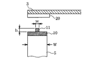
図2は、接合部の構成を示す拡大断面図である。パッケージ1の外形幅、すなわち容器2の一辺の幅を5mm以下とする場合には、枠部材5の幅Wを0.4mmとすることが望ましい。パッケージを小型化しながら内容積をある程度確保するには容器の枠幅を薄くする必要があるが、あまり薄くすると枠壁にクラックが入って気密が保てず、強度的に問題があるからである。このことを考慮すると枠部材5の幅Wは0.4mm程度が適当であり、これにあわせて枠部材5の上端面に設けられた金属層10の幅も0.4mm程度となる。
蓋3にクラッド化した封止用半田20の厚みは30μmである。これより薄くなると、加工時の圧延回数が増えるため高コストとなる。逆にこれより厚くすると半田量が多くなるため高価となる。したがって、コストとの兼ね合いから30μm厚のものが、蓋3の大きさによらず標準とされている。
そして、金属層10上の幅方向中央に設けられた上層の金属層11の幅wを約0.15mmとし、その高さhを5〜20μmに設定する。このような寸法で構成された金属層10および11からなる凸部と蓋部材3とをろう材20により接合した場合には、フィレットが正しく形成されて接合状態も良好であり、狭いシールパスでありながら接合強度も維持され、蓋部材3は収容空間12を気密に封止している。
【0007】
図3は、上層の金属層11(以下、突起という)の高さの変化に対するパッケージの良品率を示すグラフである。突起の高さの変化によって、容器1と蓋2との接合状態がどのように変化するかを示したものである。実験では、サンプル数を31個とし、ろう材として金錫半田を用い、パルスヒート方式により加熱温度320℃にて約2秒加熱した。またその良品判定は、フィレットの状態を目視にて観察し、接合部の断面を拡大鏡にて観察し、リークテストにより密封性を確認することにより行った。なお、枠部材5の幅Wは0.4mm、突起の幅wは0.15mmとしている。
これによれば、突起の高さhが5〜20μmの範囲では良品率が95%以上となり、特に突起の高さを10〜15μmとしたときには良品率が100%という良好な結果が得られた。しかし、突起の高さを0μm(突起無し)としたときには良品率が81%となり、また突起の高さを28μmとしたときには、良品率が74%という結果となった。なお枠部材5の幅Wが0.4±0.1mmと変化した場合であっても、上記と同様の結果が得られ、また突起幅を0.15±0.05mmとした場合も同様となる。
このことは、突起が高いと金属層10、11全体に熱が伝わりにくいため半田ぬれ不良となって接合不良の原因となるものと考えられ、逆に突起が低いと半田の溜まりが減少するため、半田量不足となって接合不良の原因となるものと考えられ、上記の結果は、両者の不具合を解消しうる突起の最適条件が実験的に得られたことを示しているものといえる。
以上のように、枠部材5の幅W、いいかえれば容器2の開口枠の上端面の幅Wを0.4mm±0.1mmとした場合に、金属層11からなる突起の幅を0.15±0.05mmとし、突起の高さを5〜20μmとすれば、従来の容器の開口枠の上端面に形成する金属層の高さを上下層共に30μmとした場合に比べてリーク不良の発生を防止でき、パッケージ2と蓋部材3との接合強度を高めることができ、良品率を極めて高めるものである。したがって、特にシールパスの狭い小型のパッケージにおいて、簡単な構成で気密信頼性を向上させることができる。
尚、金錫半田に限らず、融点が250℃以上のろう材を用いて、パルスヒート方式を用いた短時間の加熱工程により接合する場合であっても、上記のような接合部の構造であればフィレットが正しく形成されて、容器内の部品に加熱によるダメージを与えることなく確実な接合状態とすることができる。
【0008】
図4は、第2の実施の形態に係る電子部品用パッケージのうち接合部の構成を示す拡大断面図である。なお第1の実施形態と実質的に同一の構成要素には同一符号を付している。
第2の実施形態においては、枠部材5の上端部に段差部51を形成し、この段差部51が形成され上端面に金属層40を設けたものである。金属層40の表面にはニッケルめっきまたは金めっき、あるいはその両方が施されている。蓋3を容器2に接合した場合、金属層40と蓋3との隙間にろう材溜まり部21が形成される。
段差部51は、枠部材50となる複数枚のセラミックグリーンシートを、上層のグリーンシートの外形が下層のグリーンシートの外形よりも小さくなるように打ち抜き型やパンチングマシーン等を用いて加工し、これらを積層した後、焼成して一体化することにより、容易に形成することができる。
枠部材5の幅Wは0.4mm程度であり、段差部51の端部に形成される金属層40の上段部分の幅wを約0.15mmとし、その高さhを5〜20μmに設定する。このような寸法で構成された段差部51および金属層40からなる凸部と蓋部材3とをろう材20により接合した場合には、フィレットが正しく形成されて接合状態も良好であり、狭いシールパスでありながら接合強度も維持され、蓋部材3は収容空間12を気密に封止している。
以上のように、第2の実施形態においては、枠部材5の幅W、いいかえれば容器2の開口枠の上端面の幅Wを0.4mm±0.1mmとした場合に、その上端面に形成する金属層からなる突起の幅を0.15±0.05mmとし、突起の高さを5〜20μmとすれば、第1の実施形態と同様にリーク不良の発生を防止でき、パッケージ2と蓋部材3との接合強度を高めることができ、良品率を極めて高めるものである。
【0009】
なお、上述した複数の実施形態では、ろう材として金錫半田を用いたが、本発明はこれに限らず、融点250℃以上の高温半田であれば適用可能である。
また、上述した複数の実施形態では、金属製の蓋部材3により収容空間12を気密に封止したが、本発明では、封止部となるところに導体ペーストが印刷、焼成されたセラミックス製蓋部材により収容空間を気密に封止してもよい。
また、上述した複数の実施形態では、アルミナ製パッケージに本発明を適用したが、本発明では、アルミナに限らず、窒化アルミニウム、ムライト、ガラス等のセラミックあるいはその他の絶縁材料製のパッケージに適用してもよい。
また、上述した複数の実施形態では、片端固定方式の表面実装型圧電装置に本発明を適用したが、両端固定方式の表面実装型圧電装置に適用可能なことはいうまでもない。
また、上述した複数の実施形態では、圧電素子として表面実装型水晶振動子を例に説明したが、本発明はこれに限定されるものではなく、タンタル酸リチウム、ニオブ酸リチウム、四ほう酸リチウムもしくは圧電セラミックで構成する圧電振動子、弾性表面波素子等を用いた共振子もしくはフィルタにも適用可能である。
また、上述した複数の実施形態では、パッケージ内に圧電素子を単体で収容したものを例に説明したが、本発明はこれに限定されるものではなく、パッケージ内に圧電素子とともにIC等の発振回路を備えて構成した発振器等の電子部品、あるいは半導体素子やチップコンデンサ等の電子部品に適用してもよい。
【0010】
【発明の効果】
以上説明したように、本発明によれば、電子部品を収容する上面が開口した箱型の容器と、当該容器の開口枠の上端に密着して容器内部を封止する蓋とからなる電子部品用パッケージにおいて、前記容器の開口枠の上端面に形成された第1の金属層と、前記第1の金属層上の幅方向中央に設けられた第2の金属層とを有し、前記容器の開口枠の幅を0.4±0.1mmとし、前記第2の金属層の幅を0.15±0.05mmとしかつその高さを5乃至20μmとしたので、第1および第2の金属層からなる凸部と蓋とをろう材により接合した場合には、前記蓋が収容空間を気密に封止しており、フィレットが正しく形成されて接合状態も良好であり、狭いシールパスでありながら接合強度も維持され、良品率が95%以上という結果を得ることができる。また、融点250℃以上の金錫半田をろう材として用いて、パルスヒート方式を用いた短時間の加熱工程により接合する場合であっても、上記のような接合部の構造であればフィレットが正しく形成されて、容器内の部品に加熱によるダメージを与えることなく確実な接合状態とすることができる。
また、本発明は、電子部品を収容する上面が開口した箱型の容器と、当該容器の開口枠の上端に密着して容器内部を封止する蓋とからなる電子部品用パッケージにおいて、前記容器の開口枠の上端面に形成された第1の金属層と、前記第1の金属層上の幅方向中央に設けられた第2の金属層とを有し、前記容器の開口枠の幅を0.4±0.1mmとし、前記第2の金属層の幅を0.15±0.05mmかつその高さを10乃至15μmとしたので、請求項1記載の発明の効果に加えて、さらに良品率が100%という結果を得ることができる。
【図面の簡単な説明】
【図1】 第1の実施の形態に係る電子部品用パッケージの構造を示す側面断面図。
【図2】 接合部の構成を示す拡大断面図。
【図3】 金属層11(突起)の高さの変化に対するパッケージの良品率のグラフを示す図。
【図4】 第2の実施の形態に係る電子部品用パッケージのうち接合部の構成を示す拡大断面図。
【図5】 従来の電子部品要パッケージの構造を示す図。
【図6】 従来のパッケージにおけるフィレットの形成状態を示す図。
【符号の説明】
1 電子部品用パッケージ、2 容器、3 蓋、4 板部材、5 枠部材、6 絶縁膜、7 固定電極、8 導電性接着剤、9 接続電極、10、11 金属層(接合部)、 12 収容空間、20、30 ろう材、21、31 ろう材溜まり部、40 金属層(接合部)、51 段差部[0001]
BACKGROUND OF THE INVENTION
The present invention relates to an electronic component package that accommodates an electronic component such as a piezoelectric element.
[0002]
[Prior art]
Conventionally, as a surface-mount type piezoelectric device, a piezoelectric element such as a crystal resonator is accommodated inside a container made of an insulating material such as ceramics, and the inside of the container is hermetically sealed using a metal lid. Is generally known.
As shown in FIG. 5, when a lid is joined to the opening frame of the
However, when a container with a narrow seal path and a lid are joined using solder for brazing as a brazing material, due to fluctuations in the sealing conditions such as temperature and load when the brazing material is heated and melted, voids are trapped in the brazing material. When it generate | occur | produces, there exists a problem of causing the short circuit defect of a piezoelectric element etc. because the joining strength between a container and a cover falls or a brazing material hangs down inside a container.
For this reason, in the invention described in Japanese Patent Application Laid-Open No. 2000-294664, a lower metal layer is formed on the end face of the opening frame of the container, and an upper metal layer having a width narrower than the lower metal layer is provided on the lower metal layer. A solder pool portion is formed between the convex portion formed by the above and the lid. According to this, since the brazing material is stored in the brazing material reservoir portion and does not sag into the accommodation space of the piezoelectric element and has no voids, it prevents the occurrence of short-circuit failure and the bonding area. This increases the joint strength and improves the airtight reliability. Note that the thickness (height) of the metal layer at this time is 30 μm for both the lower layer and the upper layer according to Japanese Patent Laid-Open No. 2000-294664, and shrinkage of about 10% occurs due to firing, so the actual thickness is about 27 μm. It becomes a metal layer.
[0003]
[Problems to be solved by the invention]
By the way, with recent miniaturization of electronic devices, there is a strong demand for miniaturization of mounted parts, and miniaturization of piezoelectric devices is also being promoted. When the entire size is reduced in this way, the width W of the opening frame of the container must be reduced accordingly, as shown in FIG. 5, and particularly when one side L of the container becomes 5 mm or less, The width W of the opening frame of the container must be 0.4 mm or less.
However, if the width W of the opening frame is made as thin as 0.4 mm or less while the height of the metal layer formed on the upper end surface of the opening frame of the container is kept at 30 μm for both upper and lower layers as in the conventional case, poor bonding is likely to occur. Become. That is, when the width W of the opening frame is secured to some extent, as shown in FIG. 6A, the fillet is correctly formed and a reliable joining state is obtained, but the wettability of the
Such a problem often occurs particularly when the high-temperature solder is melted and bonded by a short heating process using the pulse heat method. As disclosed in JP-A-11-214551, this pulse heat method is a heating method that uses Joule heat that is generated when a pulsed large current is passed through a high resistance material. If pulse heat is applied from the lid side while a load is applied between the two, heat is transferred in the order of the lid → solder → metal layer on the upper end surface of the opening frame, and the solder instantaneously melts, so the container and lid are instantly fixed. It can be made to. For this reason, when it is not desired to damage parts in the container due to heating, this pulse heat method must be adopted, and measures for eliminating the above-described problems are required.
The present invention has been made in view of the above, prevents the brazing material from sagging at the joint between the container and the lid, and does not cause joint failure in the joint caused by downsizing of the package. The object is to provide a package for electronic parts with a high yield rate.
[0004]
In order to solve the above-mentioned problem, the invention according to
According to a second aspect of the present invention, there is provided an electronic component package comprising: a box-shaped container having an open upper surface for accommodating an electronic component; and a lid that is in close contact with the upper end of the opening frame of the container and seals the inside of the container. In this case, a metal layer is formed on the upper end surface of the opening frame, and the metal layer has a convex portion on the upper side, and the width of the opening frame is set to 0.4 ± 0.1 mm. The width of the portion is 0.15 ± 0.05 mm, the height of the convex portion is 10 to 15 μm, the lid has a metal surface at least at a portion joined to the opening frame, and the metal surface of the lid And brazing the brazing material, joining the metal layer of the container and the metal surface of the lid with the brazing material, and a pulse heat system between the metal layer of the container and the metal surface of the lid It is characterized by being joined by the heating method.
According to a third aspect of the present invention, there is provided an electronic component package comprising: a box-shaped container having an open upper surface for accommodating an electronic component; and a lid that is in close contact with the upper end of the opening frame of the container and seals the inside of the container. In this case, a first metal layer is provided on the upper end surface of the opening frame, and a second metal layer is provided in the center in the width direction on the first metal layer. 0.4 ± 0.1 mm, the width of the second metal layer is 0.15 ± 0.05 mm, the height of the second metal layer is 5 to 20 μm, and the lid includes at least the opening frame. A metal surface at a portion to be joined, and brazing a brazing material on the metal surface of the lid, joining the metal layer of the container and the metal surface of the lid with the brazing material, The metal layer of the container and the metal surface of the lid are joined by a pulse heat type heating method.
According to a fourth aspect of the present invention, there is provided an electronic component package comprising: a box-shaped container having an open upper surface for accommodating an electronic component; and a lid that is in close contact with the upper end of the opening frame of the container and seals the inside of the container. In this case, a first metal layer is provided on the upper end surface of the opening frame, and a second metal layer is provided in the center in the width direction on the first metal layer. 0.4 ± 0.1 mm, the width of the second metal layer is 0.15 ± 0.05 mm, the height of the second metal layer is 10 to 15 μm, and the lid includes at least the opening frame. A metal surface at a portion to be joined, and brazing a brazing material on the metal surface of the lid, joining the metal layer of the container and the metal surface of the lid with the brazing material, The metal layer of the container and the metal surface of the lid are joined by a pulse heat type heating method.
[0005]
DETAILED DESCRIPTION OF THE INVENTION
Hereinafter, embodiments of the present invention will be described in detail with reference to the drawings.
FIG. 1 is a side cross-sectional view showing a structure of an electronic component package used in a one-end fixed surface mount piezoelectric device according to a first embodiment.
The surface-mount type piezoelectric device includes a crystal resonator X as an electronic component and an electronic component package (hereinafter referred to as a package) 1 that accommodates the crystal resonator X. The
Of the exposed
The fixed
The metal layers 10 and 11 are joined to the
The
In the electronic component package having the above-described structure, the
[0006]
FIG. 2 is an enlarged cross-sectional view showing the configuration of the joint. When the outer width of the
The thickness of the sealing
The width w of the
[0007]
FIG. 3 is a graph showing a non-defective product ratio with respect to a change in the height of the upper metal layer 11 (hereinafter referred to as a protrusion). It shows how the joining state of the
According to this, when the height h of the protrusion is in the range of 5 to 20 μm, the yield rate is 95% or more, and particularly when the height of the protrusion is 10 to 15 μm, the yield rate is 100%. . However, when the height of the protrusion was 0 μm (no protrusion), the yield rate was 81%, and when the height of the protrusion was 28 μm, the yield rate was 74%. Even when the width W of the
This is because if the protrusions are high, heat is not easily transmitted to the entire metal layers 10 and 11, and it is considered that solder wetting is poor, resulting in poor bonding. Conversely, if the protrusions are low, the accumulation of solder is reduced. It is considered that the amount of solder is insufficient, which causes bonding failure, and the above results can be said to indicate that the optimum conditions for protrusions that can solve both problems were experimentally obtained.
As described above, when the width W of the
Note that not only gold-tin solder, but also a brazing material having a melting point of 250 ° C. or higher, even when joining by a short heating process using a pulse heat method, the structure of the joint as described above is used. If so, the fillet is correctly formed, and a reliable joining state can be achieved without damaging the components in the container due to heating.
[0008]
FIG. 4 is an enlarged cross-sectional view illustrating a configuration of a joint portion of the electronic component package according to the second embodiment. In addition, the same code | symbol is attached | subjected to the component substantially the same as 1st Embodiment.
In the second embodiment, a stepped
The
The width W of the
As described above, in the second embodiment, when the width W of the
[0009]
In the above-described embodiments, gold-tin solder is used as the brazing material. However, the present invention is not limited to this, and any solder that has a melting point of 250 ° C. or higher can be applied.
In the above-described embodiments, the housing space 12 is hermetically sealed by the
In the above-described embodiments, the present invention is applied to an alumina package. However, the present invention is not limited to alumina, but is applied to a package made of ceramic such as aluminum nitride, mullite, glass, or other insulating materials. May be.
Further, in the above-described embodiments, the present invention is applied to the single-end fixed surface mount type piezoelectric device, but it is needless to say that the present invention can be applied to both end fixed type surface mount type piezoelectric devices.
In the above-described embodiments, the surface-mounted crystal resonator is described as an example of the piezoelectric element. However, the present invention is not limited to this, and lithium tantalate, lithium niobate, lithium tetraborate or The present invention can also be applied to a resonator or a filter using a piezoelectric vibrator, a surface acoustic wave element, or the like made of piezoelectric ceramic.
Further, in the above-described plurality of embodiments, the case where the piezoelectric element is accommodated alone in the package has been described as an example. However, the present invention is not limited to this, and the oscillation of an IC or the like together with the piezoelectric element is included in the package. You may apply to electronic components, such as an oscillator comprised with the circuit, or electronic components, such as a semiconductor element and a chip capacitor.
[0010]
【The invention's effect】
As described above, according to the present invention, an electronic component comprising a box-shaped container having an open upper surface for accommodating an electronic component, and a lid that tightly contacts the upper end of the opening frame of the container and seals the inside of the container. And a container having a first metal layer formed on an upper end surface of the opening frame of the container and a second metal layer provided at a center in the width direction on the first metal layer, Since the width of the opening frame is 0.4 ± 0.1 mm, the width of the second metal layer is 0.15 ± 0.05 mm, and the height is 5 to 20 μm, the first and second When the convex part made of a metal layer and the lid are joined with a brazing material, the lid hermetically seals the accommodation space, the fillet is correctly formed, the joined state is good, and the seal path is narrow However, the bonding strength is maintained and the yield rate is 95% or more. It can be. Further, even when a gold-tin solder having a melting point of 250 ° C. or higher is used as a brazing material and bonding is performed by a short heating process using a pulse heat method, the fillet is formed as long as the structure of the bonding portion is as described above. It is correctly formed, and it can be in a surely joined state without damaging the components in the container by heating.
Further, the present invention provides an electronic component package comprising a box-shaped container having an upper surface that opens an electronic component, and a lid that is in close contact with the upper end of the opening frame of the container and seals the inside of the container. A first metal layer formed on an upper end surface of the opening frame, and a second metal layer provided in the center in the width direction on the first metal layer, the width of the opening frame of the container 0.4 ± 0.1 mm, the width of the second metal layer is 0.15 ± 0.05 mm, and the height thereof is 10 to 15 μm. A result that the yield rate is 100% can be obtained.
[Brief description of the drawings]
FIG. 1 is a side sectional view showing a structure of an electronic component package according to a first embodiment.
FIG. 2 is an enlarged cross-sectional view illustrating a configuration of a joint portion.
FIG. 3 is a graph showing a non-defective rate of a package with respect to a change in the height of a metal layer 11 (protrusions).
FIG. 4 is an enlarged cross-sectional view illustrating a configuration of a joint portion in an electronic component package according to a second embodiment.
FIG. 5 is a view showing the structure of a conventional electronic component required package.
FIG. 6 is a view showing a fillet formation state in a conventional package.
[Explanation of symbols]
DESCRIPTION OF
Claims (4)
前記開口枠の上端面には金属層が形成されており、該金属層は上方に凸部を有するものであり、
前記開口枠の幅を0.4±0.1mmとし、
前記凸部の幅を0.15±0.05mmとし、
前記凸部の高さを5乃至20μmとし、
前記蓋は、少なくとも前記開口枠と接合される部分に金属面を有し、
前記蓋の金属面にろう材をクラッド化しておき、前記容器の金属層と前記蓋の金属面との間を該ろう材にて接合し、
前記容器の金属層と前記蓋の金属面との間をパルスヒート方式の加熱法にて接合したことを特徴とする電子部品用パッケージ。In an electronic component package comprising a box-shaped container having an open upper surface for accommodating an electronic component, and a lid that is in close contact with the upper end of the opening frame of the container and seals the inside of the container.
A metal layer is formed on the upper end surface of the opening frame, and the metal layer has a convex portion on the upper side,
The width of the opening frame is 0.4 ± 0.1 mm,
The width of the convex portion is 0.15 ± 0.05 mm,
The height of the convex portion is 5 to 20 μm,
The lid has a metal surface at least at a portion joined to the opening frame,
Brazing a brazing material on the metal surface of the lid, and joining the metal layer of the container and the metal surface of the lid with the brazing material,
A package for electronic parts, wherein a metal layer of the container and a metal surface of the lid are joined by a heating method of a pulse heat system.
前記開口枠の上端面には金属層が形成されており、該金属層は上方に凸部を有するものであり、
前記開口枠の幅を0.4±0.1mmとし、
前記凸部の幅を0.15±0.05mmとし、
前記凸部の高さを10乃至15μmとし、
前記蓋は、少なくとも前記開口枠と接合される部分に金属面を有し、
前記蓋の金属面にろう材をクラッド化しておき、前記容器の金属層と前記蓋の金属面との間を該ろう材にて接合し、
前記容器の金属層と前記蓋の金属面との間をパルスヒート方式の加熱法にて接合したことを特徴とする電子部品用パッケージ。In an electronic component package comprising a box-shaped container having an open upper surface for accommodating an electronic component, and a lid that is in close contact with the upper end of the opening frame of the container and seals the inside of the container.
A metal layer is formed on the upper end surface of the opening frame, and the metal layer has a convex portion on the upper side,
The width of the opening frame is 0.4 ± 0.1 mm,
The width of the convex portion is 0.15 ± 0.05 mm,
The height of the convex part is 10 to 15 μm,
The lid has a metal surface at least at a portion joined to the opening frame,
Brazing a brazing material on the metal surface of the lid, and joining the metal layer of the container and the metal surface of the lid with the brazing material,
A package for electronic parts, wherein a metal layer of the container and a metal surface of the lid are joined by a heating method of a pulse heat system.
前記開口枠の上端面には第1の金属層が設けられ、該第1の金属層上の幅方向中央には第2の金属層が設けられており、
前記開口枠の幅を0.4±0.1mmとし、
前記第2の金属層の幅を0.15±0.05mmとし、
前記第2の金属層の高さを5乃至20μmとし、
前記蓋は、少なくとも前記開口枠と接合される部分に金属面を有し、
前記蓋の金属面にろう材をクラッド化しておき、前記容器の金属層と前記蓋の金属面との間を該ろう材にて接合し、
前記容器の金属層と前記蓋の金属面との間をパルスヒート方式の加熱法にて接合したことを特徴とする電子部品用パッケージ。In an electronic component package comprising a box-shaped container having an open upper surface for accommodating an electronic component, and a lid that is in close contact with the upper end of the opening frame of the container and seals the inside of the container.
A first metal layer is provided on the upper end surface of the opening frame, and a second metal layer is provided at the center in the width direction on the first metal layer,
The width of the opening frame is 0.4 ± 0.1 mm,
The width of the second metal layer is 0.15 ± 0.05 mm,
The height of the second metal layer is 5 to 20 μm,
The lid has a metal surface at least at a portion joined to the opening frame,
Brazing a brazing material on the metal surface of the lid, and joining the metal layer of the container and the metal surface of the lid with the brazing material,
A package for electronic parts, wherein a metal layer of the container and a metal surface of the lid are joined by a heating method of a pulse heat system.
前記開口枠の上端面には第1の金属層が設けられ、該第1の金属層上の幅方向中央には第2の金属層が設けられており、
前記開口枠の幅を0.4±0.1mmとし、
前記第2の金属層の幅を0.15±0.05mmとし、
前記第2の金属層の高さを10乃至15μmとし、
前記蓋は、少なくとも前記開口枠と接合される部分に金属面を有し、
前記蓋の金属面にろう材をクラッド化しておき、前記容器の金属層と前記蓋の金属面との間を該ろう材にて接合し、
前記容器の金属層と前記蓋の金属面との間をパルスヒート方式の加熱法にて接合したことを特徴とする電子部品用パッケージ。In an electronic component package comprising a box-shaped container having an open upper surface for accommodating an electronic component, and a lid that is in close contact with the upper end of the opening frame of the container and seals the inside of the container.
A first metal layer is provided on the upper end surface of the opening frame, and a second metal layer is provided at the center in the width direction on the first metal layer,
The width of the opening frame is 0.4 ± 0.1 mm,
The width of the second metal layer is 0.15 ± 0.05 mm,
The height of the second metal layer is 10 to 15 μm,
The lid has a metal surface at least at a portion joined to the opening frame,
Brazing a brazing material on the metal surface of the lid, and joining the metal layer of the container and the metal surface of the lid with the brazing material,
A package for electronic parts, wherein a metal layer of the container and a metal surface of the lid are joined by a heating method of a pulse heat system.
Priority Applications (1)
| Application Number | Priority Date | Filing Date | Title |
|---|---|---|---|
| JP2001106252A JP3831937B2 (en) | 2001-04-04 | 2001-04-04 | Package for electronic components |
Applications Claiming Priority (1)
| Application Number | Priority Date | Filing Date | Title |
|---|---|---|---|
| JP2001106252A JP3831937B2 (en) | 2001-04-04 | 2001-04-04 | Package for electronic components |
Publications (3)
| Publication Number | Publication Date |
|---|---|
| JP2002299481A JP2002299481A (en) | 2002-10-11 |
| JP2002299481A5 JP2002299481A5 (en) | 2004-11-25 |
| JP3831937B2 true JP3831937B2 (en) | 2006-10-11 |
Family
ID=18958792
Family Applications (1)
| Application Number | Title | Priority Date | Filing Date |
|---|---|---|---|
| JP2001106252A Expired - Fee Related JP3831937B2 (en) | 2001-04-04 | 2001-04-04 | Package for electronic components |
Country Status (1)
| Country | Link |
|---|---|
| JP (1) | JP3831937B2 (en) |
Families Citing this family (2)
| Publication number | Priority date | Publication date | Assignee | Title |
|---|---|---|---|---|
| US7569926B2 (en) * | 2005-08-26 | 2009-08-04 | Innovative Micro Technology | Wafer level hermetic bond using metal alloy with raised feature |
| JP6305713B2 (en) * | 2013-09-24 | 2018-04-04 | Ngkエレクトロデバイス株式会社 | Manufacturing method of electronic component storage package |
-
2001
- 2001-04-04 JP JP2001106252A patent/JP3831937B2/en not_active Expired - Fee Related
Also Published As
| Publication number | Publication date |
|---|---|
| JP2002299481A (en) | 2002-10-11 |
Similar Documents
| Publication | Publication Date | Title |
|---|---|---|
| JP5024290B2 (en) | Piezoelectric vibration device | |
| JP2003318690A (en) | Quartz resonator for surface mounting | |
| WO2003044857A1 (en) | Package for electronic component, and piezoelectric vibrating device using the package for electronic component | |
| WO2011093456A1 (en) | Piezoelectric vibration device and process for producing same | |
| JP3448865B2 (en) | Electronic component package and piezoelectric vibration device | |
| JP4561521B2 (en) | Piezoelectric vibration device | |
| JP3702117B2 (en) | Electronic component equipment | |
| JP4051452B2 (en) | Piezoelectric vibrator | |
| JP3831937B2 (en) | Package for electronic components | |
| JP4427873B2 (en) | Package for piezoelectric vibration devices | |
| JP3401781B2 (en) | Electronic component package and method of manufacturing electronic component package | |
| JP2001320256A (en) | Air-tight sealing method for piezoelectric vibrating device | |
| JPH02105710A (en) | Crystal resonator | |
| JP2008186917A (en) | Electronic component housing package, electronic device, and manufacturing method thereof | |
| JP4042150B2 (en) | Piezoelectric vibration device | |
| JP2008011125A (en) | Surface acoustic wave device | |
| JP3398295B2 (en) | Piezoelectric component and method of manufacturing the same | |
| JP3893617B2 (en) | Package for electronic components | |
| JP2015126374A (en) | Crystal oscillator | |
| JP2001156193A (en) | Electronic component device | |
| JP4599145B2 (en) | Piezoelectric diaphragm | |
| JP3438224B2 (en) | Piezoelectric vibration device | |
| JP2022102015A (en) | Package, lid, and manufacturing method for package | |
| JP2000294664A (en) | Package for electronic part | |
| JP2004103626A (en) | Sealing structure of ceramic package |
Legal Events
| Date | Code | Title | Description |
|---|---|---|---|
| A977 | Report on retrieval |
Free format text: JAPANESE INTERMEDIATE CODE: A971007 Effective date: 20050228 |
|
| A131 | Notification of reasons for refusal |
Free format text: JAPANESE INTERMEDIATE CODE: A131 Effective date: 20060116 |
|
| A521 | Written amendment |
Free format text: JAPANESE INTERMEDIATE CODE: A523 Effective date: 20060302 |
|
| A131 | Notification of reasons for refusal |
Free format text: JAPANESE INTERMEDIATE CODE: A131 Effective date: 20060327 |
|
| A521 | Written amendment |
Free format text: JAPANESE INTERMEDIATE CODE: A523 Effective date: 20060526 |
|
| TRDD | Decision of grant or rejection written | ||
| A01 | Written decision to grant a patent or to grant a registration (utility model) |
Free format text: JAPANESE INTERMEDIATE CODE: A01 Effective date: 20060626 |
|
| A61 | First payment of annual fees (during grant procedure) |
Free format text: JAPANESE INTERMEDIATE CODE: A61 Effective date: 20060709 |
|
| R150 | Certificate of patent or registration of utility model |
Free format text: JAPANESE INTERMEDIATE CODE: R150 |
|
| FPAY | Renewal fee payment (event date is renewal date of database) |
Free format text: PAYMENT UNTIL: 20100728 Year of fee payment: 4 |
|
| FPAY | Renewal fee payment (event date is renewal date of database) |
Free format text: PAYMENT UNTIL: 20110728 Year of fee payment: 5 |
|
| FPAY | Renewal fee payment (event date is renewal date of database) |
Free format text: PAYMENT UNTIL: 20110728 Year of fee payment: 5 |
|
| FPAY | Renewal fee payment (event date is renewal date of database) |
Free format text: PAYMENT UNTIL: 20120728 Year of fee payment: 6 |
|
| FPAY | Renewal fee payment (event date is renewal date of database) |
Free format text: PAYMENT UNTIL: 20120728 Year of fee payment: 6 |
|
| S111 | Request for change of ownership or part of ownership |
Free format text: JAPANESE INTERMEDIATE CODE: R313111 |
|
| FPAY | Renewal fee payment (event date is renewal date of database) |
Free format text: PAYMENT UNTIL: 20120728 Year of fee payment: 6 |
|
| R371 | Transfer withdrawn |
Free format text: JAPANESE INTERMEDIATE CODE: R371 |
|
| FPAY | Renewal fee payment (event date is renewal date of database) |
Free format text: PAYMENT UNTIL: 20120728 Year of fee payment: 6 |
|
| S111 | Request for change of ownership or part of ownership |
Free format text: JAPANESE INTERMEDIATE CODE: R313111 |
|
| FPAY | Renewal fee payment (event date is renewal date of database) |
Free format text: PAYMENT UNTIL: 20120728 Year of fee payment: 6 |
|
| R350 | Written notification of registration of transfer |
Free format text: JAPANESE INTERMEDIATE CODE: R350 |
|
| FPAY | Renewal fee payment (event date is renewal date of database) |
Free format text: PAYMENT UNTIL: 20120728 Year of fee payment: 6 |
|
| FPAY | Renewal fee payment (event date is renewal date of database) |
Free format text: PAYMENT UNTIL: 20130728 Year of fee payment: 7 |
|
| LAPS | Cancellation because of no payment of annual fees |