JP3831418B2 - Imaging device - Google Patents
Imaging device Download PDFInfo
- Publication number
- JP3831418B2 JP3831418B2 JP05994294A JP5994294A JP3831418B2 JP 3831418 B2 JP3831418 B2 JP 3831418B2 JP 05994294 A JP05994294 A JP 05994294A JP 5994294 A JP5994294 A JP 5994294A JP 3831418 B2 JP3831418 B2 JP 3831418B2
- Authority
- JP
- Japan
- Prior art keywords
- signal
- pixel
- image sensor
- pixel signal
- read
- Prior art date
- Legal status (The legal status is an assumption and is not a legal conclusion. Google has not performed a legal analysis and makes no representation as to the accuracy of the status listed.)
- Expired - Fee Related
Links
Images


Description
【0001】
【産業上の利用分野】
本発明は、CCD等の固体撮像素子により得られた画素信号に基づいて、測光・測距動作を行うとともに、静止画の映像信号を生成する装置に関する。
【0002】
【従来の技術】
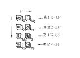
従来撮像装置として、イメージセンサの受光面上に、マゼンタ、グリーン、イエローおよびシアンの色フィルタ要素を規則的に配設して成る補色市松カラーフィルタが設けられたものが知られている。この撮像装置において、フレームモードの映像信号を生成する場合、イメージセンサから、奇数行目の画素信号とこの行の下側に隣接する行の画素信号とを加算して奇数フィールドの画素信号を読み出し、また偶数行目の画素信号とこの行の下側に隣接する行の画素信号とを加算して偶数フィールドの画素信号を読み出している。すなわち、1フィールドの画素信号はイメージセンサから2行ずつ同時に読み出されて生成され、奇数フィールドと偶数フィールドの画素信号から1画面の映像信号が得られている。
【0003】
また従来、上述した撮像装置により測光・測距動作を行う場合、イメージセンサから2行ずつ同時に読み出された1フィールドの画素信号に基づいて輝度信号を生成し、この輝度信号に基づいて測距データ等が計算されている。
【0004】
【発明が解決しようとする課題】
上述した補色市松カラーフィルタを有する従来の撮像装置では、色に対する解像度が低い。そこで本出願人は特願平4-262810号において、色解像度を高める構成として、2つのイメージセンサを設け、各イメージセンサから画素信号を1行ずつ読み出すとともに所定の画素信号どうしを重ね合わせて、静止画の映像信号(R信号、G信号およびB信号)を得る構成を提案した。
【0005】
ところがこの提案装置において、測光・測距動作のために、イメージセンサから2行ずつ同時に画素信号を読み出して輝度信号を生成するような制御を行うと、A/D変換器のダイナミックレンジが1行読み出しの場合(静止画の映像信号の生成時)とは異なるため、A/D変換を高精度に行うためには2種類のA/D変換器を設けることが必要となり、装置の製造コストが高くなるという問題が発生する。
【0006】
本発明は、撮像素子を複数有する撮像装置において、静止画の画質向上を図るとともに、測光範囲の拡大し、かつ量子化におけるダイナミックレンジの適正化を同時に行なう簡略な構成な撮像装置を得ることを目的としている。
【0007】
【問題を解決するための手段】
本発明に係る撮像装置は、水平方向および垂直方向に沿って並ぶ各画素の画素信号を生成する複数のイメージセンサと、水平方向に沿って1行ずつ画素信号を読み出す第1の読出モード、または水平方向に沿って隣接する行の画素信号を加算して読み出す第2の読出モードにより、イメージセンサから画素信号を読み出す画素信号読出手段と、この画素信号読出手段により読み出された画素信号を、第1および第2の読出モードにおいてほぼ同じダイナミックレンジで量子化するA/D変換手段と、第2の読出モードに従って各イメージセンサから読み出された1フィールドの画素信号に基づいて、測光演算または測距演算のための輝度信号を生成する輝度信号生成手段と、第1の読出モードに従ってイメージセンサから読み出された画素信号に基づいて、静止画の映像信号を生成する映像信号生成手段とを備え、輝度信号生成手段は、各イメージセンサが相互に異なる電子シャッタスピードで露光されるとき、各イメージセンサから読み出された画素信号に基づいて被写体輝度を求めることを特徴としている。
【0008】
【実施例】
以下図示実施例により本発明を説明する。
図1は本発明の第1実施例である撮像装置を備えたスチルビデオカメラのブロック図である。
【0009】
システム制御回路10はマイクロコンピュータであり、本スチルビデオカメラの全体の制御を行う。
【0010】
フォーカスレンズ11は合焦動作時、フォーカレンズ駆動回路12によって制御される。絞り13は露出制御時、絞り駆動回路14によって開度を調整される。フォーカレンズ駆動回路12と絞り駆動回路14は、システム制御回路10によって制御される。
【0011】
フォーカスレンズ11と絞り13を通った光線は、ハーフミラー15a、15bにより分割される。1つの光線は図示しないファインダへ導かれ、他の2つの光線は第1および第2のCCD(イメージセンサ)16、17に導かれる。これらのCCD16、17は、各受光面に等価な被写体像が結像されるように配置されている。CCD16、17は固体撮像素子であり、再生画面の水平方向および垂直方向に沿って並ぶ多数の画素に対応したフォトダイオードを有し、これらのフォトダイオードには被写体像に対応した画素信号が発生する。
【0012】
第1および第2のCCD16、17には、それぞれフィルタ21、22が設けられる。これらのCCD16、17はCCD駆動回路23によって駆動され、これにより、CCD16、17上に結像された被写体像に対応した画素信号が、相関二重サンプリング(CDS)回路24、25に供給される。CCD駆動回路23は、システム制御回路10によって制御される。
【0013】
CDS回路24、25に入力された画素信号は、リセット雑音の除去等の所定の処理を施される。CDS回路24、25から出力された信号は、増幅器26、27を介して、または増幅器26、27を通らずにA/D変換器31、32に入力される。後述するように、CCD16、17からの画素信号の読出動作として第1および第2の読出モードがあり、増幅器26、27は第1の読出モードが選択された時、この画素信号の電圧レベルを増幅するために設けられている。スイッチ28、29はA/D変換器31、32を増幅器26、27あるいはCDS回路24、25に接続させるために設けられており、これらのスイッチ28、29の切り換え制御はシステム制御回路10により行われる。
【0014】
A/D変換器31、32によりデジタル信号に変換された画素信号は、第1および第2の画像メモリ33、34にそれぞれ格納される。各画像メモリ33、34はそれぞれ2フィールド分の画素信号を格納できる記憶容量を有している。画像メモリ33、34のアドレス制御は、システム制御回路10により画像メモリ制御回路35を介して行われる。
【0015】
画像メモリ33、34から読み出された画素信号は映像信号処理回路36に入力され、所定の処理を施されてR信号、G信号およびB信号に変換される。これらの信号はインターフェイス回路37に入力され、メモリカード38に記録するためのフォーマットに変換される。メモリカード38へのR信号、G信号およびB信号の記録動作は、システム制御回路10によりメモリカード制御回路39を介して行われる。
【0016】
システム制御回路10には、レリーズボタン41が接続されている。後述するように、レリーズボタン41を半押しすることにより、測光・測距動作が行われ、全押しすることにより、映像信号のメモリカード38への記録動作が行われる。またシステム制御回路10には赤外線三角測距装置42が接続されている。この測距装置42は従来公知のように、被写体に向けて赤外線を照射し、この赤外線の被写体からの反射光を受光することにより、三角測距によって被写体までの距離を測定するものである。
【0017】
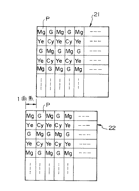
図2は第1および第2のCCD16、17の受光面上に設けられたカラーフィルタ21、22の配列を示すものである。これらのカラーフィルタ21、22は、補色市松カラーフィルタであり、同じ構成を有している。これらのカラーフィルタ21、22では、マゼンタ(Mg)、イエロー(Ye)、シアン(Ce)およびグリーン(G)を透過させる各フィルタ要素が規則的に配置されている。すなわち、水平方向および垂直方向にそれぞれ2画素ずつ並べて成る計4画素には、グリーン(G)の他に、補色の異なる分光特性を有するマゼンタ(Mg)、イエロー(Ye)およびシアン(Ce)の3画素が設けられている。
【0018】
第2のカラーフィルタ22のCCD17に対する位置関係を、第1のカラーフィルタ21のCCD16に対する位置関係と比較すると、第2のカラーフィルタ22は、CCD17に対し1画素分だけ水平方向(図2では左方向)にずらせて設けられている。例えば画面の左上隅の画素Pに注目すると、第1のカラーフィルタ21ではマゼンタであるが、第2のカラーフィルタ22ではグリーンである。
【0019】
このようにCCD16、17の画素分光特性は、それぞれ規則的に変化しており、補色色差線順次式である。また、第1のCCD16の画素分光特性に対して、第2のCCD17の画素分光特性は1画素分だけ水平方向にずれている。したがって、第1のCCD16の垂直方向に並ぶ2画素と、その2画素の光学的に同じ位置にある第2のCCD17の垂直方向に並ぶ2画素との4画素は、それぞれ異なる分光特性を有している。すなわち、例えば一方の2画素がMgとYeである場合、他方の2画素はGとCyである。
【0020】
第1のCCD16の出力信号と第2のCCD17の出力信号は、デジタル信号として画像メモリ33、34に一旦格納されるが、これらのメモリから読み出され、映像信号処理回路36において処理される。すなわち、対応する画素同士が相互に重ね合わせられるとともに、この重ね合わされた信号から各画素に対応するR信号、G信号およびB信号が抽出されて映像信号が得られる。
【0021】
図3はこの重ね合わせの状態を示している。この図から理解されるように、第1のCCD16のフィルタ21のマゼンタ(Mg)と第2のCCD17のフィルタ22のグリーン(G)が、フィルタ21のグリーン(G)とフィルタ22のマゼンタ(Mg)が、フィルタ21のイエロー(Ye)とフィルタ22のシアン(Cy)が、フィルタ21のシアン(Cy)とフィルタ22のイエロー(Ye)が、それぞれ同じ画素に対応している。なお図3において、Pxは水平方向の各画素の間隔(1ピッチ)、Pyは垂直方向の各画素の間隔(1ピッチ)をそれぞれ示す。
【0022】
まずR信号の抽出について説明する。
マゼンタ(Mg)に含まれるR信号をRMg、B信号をBMg、イエロー(Ye)に含まれるR信号をRYe、G信号をGYe、シアン(Cy)に含まれるG信号をGCy、B信号をBCyとすると、
Mg= RMg+BMg、Ye= RYe+GYe、Cy= GCy+BCy
と表すことができる。
【0023】
R信号は、垂直方向に並ぶマゼンタ(Mg)とイエロー(Ye)、およびこれらに重ね合わされたグリーン(G)とシアン(Cy)の4画素(図3において斜線を付された画素)から、次の式により得られる。
α=GYe/(G+GCy)=BMg/BCy
が成立することが条件である。
【0024】
B信号についても同様に、次の式により得られる。
β=GCy/(G+GYe)=RMg/RYe
が成立することが条件である。
【0025】
G信号については、輝度信号Yと、(1)式、(2)式により求められたRS 、BS とから得られる。すなわち、
次に図4を参照してRGB信号の実際の抽出方法について説明する。
この図の画素配置において、第1および第2のCCD16、17をそれぞれパラメータA、Bで表し、水平方向をパラメータi、垂直方向をパラメータjで表す。なおこの図において、重ね合わせて示された各画素のうち上方に位置するものが第1のCCD16に対応し、下方に位置するものが第2のCCD17に対応するものとする。各画素からの信号を、第1のCCD16に関しては、
VA,i,j =Mg、VA,i+1,j =G
VA,i,j+1=Ye、VA,i+1,j+1 =Cy
VA,i,j+2 =G 、VA,i+1,j+2 =Mg
VA,i,j+3 =Ye、VA,i+1,j+3 =Cy
となるように配置し、第2のCCD17に関しては、
VB,i,j =G 、VB,i+1,j =Mg
VB,i,j+1 =Cy、VB,i+1,j+1 =Ye
VB,i,j+2 =Mg、VB,i+1,j+2 =G
VB,i,j+3 =Cy、VB,i+1,j+3 =Ye
となるように配置する。ここで、i=1,3,5,...;j=1,5,9,... の値をとるものとする。
【0027】
一回目の走査で第1フィールドの信号すなわち、
VA,i,j =Mg、VA,i+1,j =G
VA,i,j+2 =G 、VA,i+1,j+2 =Mg
VB,i,j =G 、VB,i+1,j =Mg
VB,i,j+2 =Mg、VB,i+1,j+2 =G
が抽出され、二回目の走査で第2フィールドの信号すなわち、
VA,i,j+1 =Ye、VA,i+1,j+1 =Cy
VA,i,j+3 =Ye、VA,i+1,j+3 =Cy
VB,i,j+1 =Cy、VB,i+1,j+1 =Ye
VB,i,j+3 =Cy、VB,i+1,j+3 =Ye
が抽出される。
【0028】
以上の全画素信号が画像メモリ33、34に記憶される。これらの画素信号は映像信号処理回路36に読み出され、演算により奇数フィールドの奇偶数走査線のi番目の画素に対し、
【0029】
同様にして、奇数フィールドの奇偶数走査線のi+1番目の画素に対し、
ここで、p,q は(3)式を参照すれば1であっても良いが、Y成分の値に応じ、適当に調整できる方が好ましい。
【0030】
α、β、p、qの定数は、システム制御回路10において実行されるソフトウェアのパラメータを調整することによって定められる。
【0031】
偶数フィールドについては、j+1番目とj+2番目の画素を組み合わせることにより、上記(4)〜(15)式と同様な式によりRGB信号が得られる。
なお、以上の式はガンマ補正を施していないリニアな演算方法であり、ガンマ補正された信号が画像メモリ33、34に記憶されているのであれば、一旦リニアに変換した後、それらの演算が行われ、その演算後、正規のガンマ補正が行われる。
【0032】
次に図5〜図11を参照して、第1実施例における撮影動作を説明する。図5と図6は測距・測光動作を行うプログラムのフローチャートであり、図7は映像信号のメモリカードへの記録動作を行うプログラムのフローチャートである。図8は撮影動作のタイミングチャートである。図9は自動焦点調節(AF)動作におけるフォーカスレンズの移動を示す図である。図10は第2の読出モードにおける画素信号の読出動作を示す図である。図11は第1の読出モードにおける画素信号の読出動作を示す図である。
【0033】
図5と図6に示す測距・測光動作のプログラムの実行は、レリーズボタン41を半押しする(符号A1)ことにより開始する。ステップ101では、赤外線三角測距装置42により赤外線三角測距が行われ(符号A2)、本スチルビデオカメラから被写体までの距離が測定される。赤外線三角測距の精度は、図9に示す各赤外測距ゾーンZ1、Z2・・・ZNの大きさに対応しており、後述するCCDを用いた測距の精度よりも粗い。この赤外線三角測距の結果、フォーカスレンズ11は合焦のために、赤外測距ゾーンZNに位置すべきであると判断された場合、ステップ102において、フォーカスレンズ11は現在位置(符号TL)から、その赤外測距ゾーンZNの中で最も現在位置TLに近い端(X位置)まで移動する(符号A3)。
【0034】
ステップ103〜105では、絞り13が開放位置に定められた状態で測光動作が行われる。この測光動作およびステップ107以下の測距動作におけるCCD16、17からの画素信号の読出動作は、第2の読出モードにより行われる。第2の読出モードとは、次に述べるように、水平方向に沿って隣接する行の画素信号を加算して読み出すモードである。
【0035】
ここで図10を参照して、第2の読出モードにより読み出された画素信号に基づいて輝度信号を求める方法を説明する。第2の読出モードでは、第1および第2の水平方向のラインL1、L2が加算され、また第3および第4の水平方向のラインL3、L4が加算されて読み出され、これらのラインにより第1フィールドが形成される。輝度信号Yは、次の(16)式により表される。
(16)式から理解されるように、図10において例えば二点鎖線YYにより囲まれるMg、Ye、G、Cyの4画素の信号を加算することにより、輝度信号が得られる。
【0037】
なお第2の読出モードでは、図1に示すように、スイッチ28、29は増幅器26、27とは反対側に切り換えられており、CDS回路24、25の出力信号は、増幅器26、27を通らずにA/D変換器31、32に入力される。したがって、この読出モードでは、CDS回路24、25の出力信号は増幅されずにA/D変換器31、32に入力される。
【0038】
さてステップ103では、第1および第2のCCD16、17が相互に異なる所定の電子シャッタスピードで露光される。すなわち、第1のCCD16に対しては相対的に長い第1の電子シャッタスピードで露光が行われ(符号A4)、第2のCCD17に対しては相対的に短い第2の電子シャッタスピードで露光が行われる(符号A5)。このように2つの異なる電子シャッタスピードでCCD16、17が露光されることにより、後述するように、CCDを1つだけ用いる場合と比較して、より広い測光範囲が得られる。
【0039】
ステップ104では、第1および第2のCCD16、17により得られた撮像信号が第1および第2の画像メモリ33、34へ取り込まれる(符号A6、A7)。すなわち各画像メモリ33、34には、それぞれ1フィールドの画素信号が測光データとして格納される。ステップ105では、画像メモリ33、34に格納された測光データのうち所定のデータを用いて被写体輝度が求められる。すなわち、例えば画面中央の画素に対応する測光データであって、CCD16、17のダイナミックレンジ内のデータを用い、(16)式に基づいて1画素に対応する輝度値が求められる。さらに画面中央の各画素に対する輝度値を平均して、被写体輝度が求められる(符号A8)。
【0040】
ステップ106では、ステップ105において求められた被写体輝度とCCD16、17の感度に基づいて、適正露出が得られるような2つの電子シャッタスピードが求められる。すなわち、
(1)絞りが開放位置にある状態における電子シャッタスピード
(2)所定のプログラム線図に従った絞り値と電子シャッタスピード
が求められる(符号A8)。
【0041】
(1)の電子シャッタスピードは、ステップ107以下で実行される測距動作において用いられる。すなわち絞り13が開放された状態で測距動作が行われ、合焦動作が行われる。 (2)の電子シャッタスピードは、図7に示す映像信号の記録動作において用いられる。
【0042】
ステップ103〜105の測光動作では、第1および第2のCCD16、17が用いられたが、以下に述べる測距動作では、第1のCCD16のみが用いられ、第2のCCD17の画素信号は無視される。
【0043】
ステップ107では、 (1)の電子シャッタスピードで第1のCCD16が露光され(符号A9)、ステップ108では、第1のCCD16の撮像信号が第1の画像メモリ33に取り込まれる(符号A10)。ステップ109では、第1の画像メモリ33に格納されたデータのうち所定範囲のデータを用いてフォーカス評価値Aが求められる(符号A11)。このフォーカス評価値Aは例えば、(16)式に基づく所定の画素に対応する輝度値と、この画素の周囲の画素に対応する輝度値との差分値(すなわち微分値)を求めることにより得られ、従来公知の種々の方法を用いることができる。
【0044】
次いでステップ110では、図9に示すように、現在フォーカスレンズ11が位置している赤外線三角測距ゾーンZNのほぼ中央(Y位置)まで、フォーカスレンズ11が移動する(符号A12)。
【0045】
ステップ111〜114の作用は、ステップ107〜110と同様である。すなわちフォーカスレンズ11がY位置に定められた状態で、ステップ111において、CCD16が露光され(符号A13)、ステップ112において、CCD16の撮像信号が画像メモリ33に取り込まれる(符号A14)。ステップ113では、画像メモリ33に格納されたデータからフォーカス評価値Bが求められる(符号A15)。ステップ114では、図9に示すように、フォーカスレンズ11は赤外線三角測距ゾーンZNの後端(Z位置)まで移動する(符号A16)。
【0046】
そして上記と同様にして、フォーカスレンズ11がZ位置に定められた状態で、ステップ115では、CCD16が露光され(符号A17)、ステップ116では、CCD16の撮像信号が画像メモリ33に取り込まれる(符号A18)。ステップ117では、画像メモリ33に格納されたデータからフォーカス評価値Cが求められる(符号A19)。
【0047】
ステップ118では、フォーカス評価値A、B、Cの中で最も良い値、すなわち最も大きいフォーカス評価値を示す位置まで、フォーカスレンズ11が移動し(符号A20)、AF動作は終了する。なお、図9の例では、フォーカスレンズ11はX位置に移動している。
【0048】
次いでレリーズボタン41が全押しされると(符号A21)、図7のプログラムの実行が開始する。ステップ201では絞り13が、レリーズボタン41の半押し時、すなわち図5と図6のプログラムのステップ106において求められた
(2)の絞り値まで駆動される(符号A22)。
【0049】
ステップ202では、このステップ106において求められた (2)の電子シャッタスピードで第1のCCD16が露光され(符号A23)、ステップ203では、このCCD16の撮像信号が第1の画像メモリ33に取り込まれる(符号A24)。この露光は、上述したようにプログラム線図に従った絞り値と電子シャッタスピードにより行われるため、これにより適正な露光量が得られるはずであるが、上述した測光・測距動作は開放絞りで行われているため、その露光量には誤差が含まれている可能性がある。そこでステップ204では、第1の画像メモリ33から読み出された所定範囲のデータを用いて、適正な露光量が得られるように、電子シャッタスピードの補正値が求められる(符号A25)。これにより絞りの誤差が補正され、最適電子シャッタスピードが得られる。
【0050】
後述するステップ206、207では、第1の読出モードにより画素信号が読み出され、1回の読出動作ではCCD16、17においてそれぞれ半分のフォトダイオードの信号電荷が読み出される。これに対しステップ202では、第2の読出モードにより画素信号が読み出され、1回の読出動作ではCCD16において全てのフォトダイオードの信号電荷が読み出される。したがって各CCDにおいて、信号電荷が蓄積されるフォトダイオードの数が異なることも考慮され、最適電子シャッタスピードはステップ202における電子シャッタスピードよりも短い。
【0051】
ステップ205では、図1のスイッチ28、29が増幅器26、27側に切り換えられ、CCDからの画素信号の読出モードが第1の読出モードに定められる(符号A26)。この第1の読出モードは、CCD16、17から画素信号が水平方向に沿って1行ずつ読み出されるモードである。この第1の読出モードでは、図11に示すように、まず水平方向のラインM1、M3・・・を構成する画素信号から成る第1フィールドが1ライン毎に読み出され、次いで、水平方向のラインM2、M4・・・を構成する画素信号から成る第2フィールドが1ライン毎に読み出される。
【0052】
また第1の読出モードでは、スイッチ28、29が増幅器26、27側に切り換えられているので、CDS回路24、25の出力信号は、増幅器26、27を通ってA/D変換器31、32に入力される。すなわちCDS回路24、25の出力信号は増幅器26、27により所定の増幅率で増幅されて、A/D変換器31、32に入力される。
【0053】
ステップ206では、ステップ204において求められた最適電子シャッタスピードで、第1および第2のCCD16、17が露光される(符号A27)。これは本露光であり、第1および第2のCCD16、17に生成された撮像信号は、ステップ207において、これらのCCD16、17から読み出され、それぞれ第1および第2の画像メモリ33、34に取り込まれる(符号A28)。上述したように、この読出動作は第1の読出モードにより行われ、まず第1フィールドの画素信号が画像メモリ33、34への取り込まれる。
【0054】
この画像メモリへの取り込みと並行して、残りの画素に対する露光が行われる(符号A29)。すなわち、画素信号を一度掃き出した後(図示せず)、最適電子シャッタスピードで再び露光が行われる。ステップ208では、第1および第2のCCD16、17の残りの画素に生成された撮像信号が、それぞれ第1および第2の画像メモリ33、34に取り込まれる(符号A30)。この時、取り込まれる画素信号は第2フィールドの信号であり、ステップ207と合わせると、それぞれの画像メモリ33、34には2フィールド分の画素信号が取り込まれたことになる。
【0055】
なお、レリーズボタン41の全押しのタイミングによって第2フィールドの画素信号を第1フィールドの画素信号よりも先にメモリ33、34に取り込むようにしてもよい。
【0056】
次いでステップ209では、絞り13が開放位置に定められ(符号A31)、ステップ210では、CCDからの画素信号の読出モードが第2の読出モードに切り換えられる(符号A32)。ステップ211では、第1および第2の画像メモリ33、34から画素信号が読み出されるとともに、映像信号処理回路36においてR信号、G信号およびB信号に変換され、これらの信号はインターフェイス回路37によりメモリカード38に記録される(符号A33)。これにより、このプログラムは終了する。
【0057】
次に図12と図13を参照して、図5のステップ103〜105において実行される測光動作を説明する。図12はCCD16、17による測光範囲を示し、図13は測光動作における各信号の出力タイミングを示している。
【0058】
第1および第2のCCD16、17のダイナミックレンジVDRは同じ大きさであり、実線S1で示すように第1のCCD16による測光範囲は被写体輝度E1 〜E2 、また実線S2で示すように第2のCCD17による測光範囲は被写体輝度E2 〜E3 である。すなわち第1のCCD16の電子シャッタスピードは第2のCCD17のそれよりも長く、したがって、第1のCCD16は相対的に暗い光を検出し、第2のCCD17は相対的に明るい光を検出する。このように、2つのCCD16、17の電子シャッタスピードを変えたことにより、測光範囲(E1 〜E3 )はひとつのCCDを用いた場合と比較して、対数で2倍になっている。
【0059】
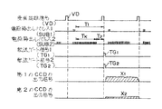
CCD16、17からの信号電荷の読み出しは次のようにして行われる。まず、垂直同期信号VDが出力された後、露光開始時点まで電荷掃き出しパルスSUB1、SUB2が定期的に出力され、CCD16、17の各フォトダイオードに残留している不要電荷がサブストレートに掃き出される。第1のCCD16に対する電荷掃き出しパルスSUB1が停止した後、所定時間TK が経過すると、第2のCCD17に対する電荷掃き出しパルスSUB2が停止する。そして、電荷掃き出しパルスSUB1が停止してから時間T1 が経過すると、2つの転送ゲート信号TG1とTG2が同時に出力され、垂直転送CCDへ各画素の信号が転送される。これにより第1のCCD16には時間T1 の間、また第2のCCD17には時間T2 (=T1 −TK )の間、それぞれ電荷が蓄積されることとなる。すなわち、時間T1 は第1のCCD16の電子シャッタスピードに相当し、時間T2 は第2のCCD17の電子シャッタスピードに相当する。
【0060】
また、2つの転送ゲートTG1、TG2が同時に出力された時、これと共に読み出し転送パルス(図示せず)が出力される。これにより、CCD16、17に蓄積されていた画素信号が第2の読出モードで読み出される。図13において、符号X1 は第1のCCD16から読み出された画素信号、符号X2 は第2のCCD17から読み出された画素信号であり、これらの画素信号X1 、X2 を用いて前記(16)式により被写体輝度が求められる。
【0061】
図14〜図16を参照して、測光・測距動作において実行される第2の読出モードにおける画素信号の読み出し動作を説明する。
【0062】
図14は、CCD16、17のフォトダイオードに発生する2つの画素信号が垂直転送CCD51、52において加算される様子を示している。なお、この図において、斜線SHで示す部分はポテンシャルの井戸を示し、各フォトダイオードから転送されてきた画素信号はこのポテンシャルの井戸において混合されることにより加算される。また、「4」、「6」等の数字は、図16に示す時間tに対応している。
【0063】
第1フィールドにおける画素信号の読み出し動作を説明する。
フォトダイオードF11、F13に蓄積したMg、G信号が垂直転送CCD51に転送され、またフォトダイオードF21、F23に蓄積したG信号、Mg信号が垂直転送CCD52に転送される(符号J1)。次いで、フォトダイオードF12、F14に蓄積したYe信号が垂直転送CCD51に転送され、またフォトダイオードF22、F24に蓄積したCy信号が垂直転送CCD52に転送される(符号J2)。
【0064】
そして垂直転送CCD51では、フォトダイオードF11のMg信号とフォトダイオードF12のYe信号とが加算され、またフォトダイオードF13のG信号とフォトダイオードF14のYe信号とが加算される。垂直転送CCD52では、フォトダイオードF21のG信号とフォトダイオードF22のCy信号とが加算され、またフォトダイオードF23のMg信号とフォトダイオードF24のCy信号とが加算される(符号J3)。その後、各垂直転送CCD51、52では垂直転送が行われ、加算された画素信号は水平転送CCD(図示せず)側に転送される(符号J4)。1回の垂直転送において、信号は2画素分転送され、この度に、水平転送CCDでは1水平走査線分の画素信号が読み出される(符号J5)。
【0065】
第2フィールドにおける画素信号の読み出し動作は第1フィールドと同様であるが、相互に加算される2つの画素信号の組合せが第1フィールドと異なる。すなわち垂直転送CCD51では、フォトダイオードF11に蓄積したMg信号は、図14の上方に隣接するフォトダイオード(図示せず)に蓄積したYe信号と加算され、フォトダイオードF12に蓄積したYe信号はフォトダイオードF13に蓄積したG信号と加算される。フォトダイオードF14に蓄積したYe信号は、図14の下方に隣接するフォトダイオード(図示せず)に蓄積したMg信号と加算される。垂直転送CCD52についても同様である。
【0066】
図16は、画素信号の転送動作を行うために電極V1〜V4に供給される電圧信号の時間的変化と、垂直転送CCDにおけるポテンシャルの井戸の時間的変化とを示している。この図に示すように、時間t=4,6において画素読み出しパルス(転送ゲート信号)が出力され、これによりフォトダイオードから画素信号が垂直転送CCD51、52に転送される。また時間t=8では、電極V1、V2、V3の電圧レベルが同じ大きさになり、これにより電極V1に対応した井戸と電極V3に対応した井戸とが合体して画素信号が加算される(符号J6)。
【0067】
図17〜図19は、本露光において実行される第1の読出モードにおける画素信号の読み出し動作を示している。
【0068】
図17は、CCD16、17のフォトダイオードに発生する画素信号が垂直転送CCD51、52に転送される様子を示している。なお、この図において、「6」、「8」等の数字は、図19に示す時間tに対応している。
【0069】
第1フィールドにおける画素信号の読み出し動作を説明する。
フォトダイオードF12、F14、F22、F24に対しては、画素読み出しパルス(転送ゲート信号)は出力されない。したがって、フォトダイオードF12、F14に蓄積したYe信号とフォトダイオードF22、F24に蓄積したCy信号は垂直転送CCD51、52に転送されず(符号J11)、フォトダイオードF11、F13に蓄積したMg信号、G信号とフォトダイオードF21、F23に蓄積したG、Mg信号だけが垂直転送CCD51、52に転送される(符号J12)。
【0070】
この後、第2の読出モードと同様に、電極V1、V2、V3の電圧レベルが同じ大きさになり、垂直転送CCD51、52においてポテンシャルの井戸SHが大きくなるが、1つの井戸SHには1つの画素信号しか転送されていないため、画素信号の加算は行われない(符号J13)。次いで、各垂直転送CCD51、52では垂直転送が行われ、画素信号は水平転送CCD(図示せず)側に転送される(符号J14)。1回の垂直転送において、信号は2画素分転送され、この度に、水平転送CCDでは1水平走査線分の画素信号が読み出される(符号J15)。
【0071】
第2フィールドにおける画素信号の読み出し動作は第1フィールドと同様である。すなわちフォトダイオードF11、F13、F21、F23に対しては、画素読み出しパルスは出力されず、したがって、これらのフォトダイオードに蓄積したG信号とMg信号は垂直転送CCD51、52に転送されない(符号J17)。一方、フォトダイオードF12、F14に蓄積したYe信号とフォトダイオードF22、F24に蓄積したCy信号だけが垂直転送CCD51、52に転送され(符号J16)、垂直転送される(符号J18)。
【0072】
図19は、第2の読出モードにおける図16に対応している。この図に示すように、時間t=6では画素読出パルスが出力されず(符号J19)、時間t=4において画素読み出しパルスが出力され、これによりフォトダイオードから画素信号が垂直転送CCD51、52に転送される。また時間t=8では、電極V1、V2、V3の電圧レベルが同じ大きさになり、これにより電極V1に対応した井戸と電極V3に対応した井戸とが合体するが、電極V3に対応した井戸には画素信号が存在しないため、画素信号の加算は行われない(符号J20)。
【0073】
以上のように第1実施例は、CCD16、17から1行ずつ画素信号を読み出す第1の読出モードでは、画素信号は増幅器26、27により増幅されてA/D変換器31、32に入力され、CCD16、17から2行ずつ画素信号を読み出す第2の読出モードでは、画素信号は増幅器26、27を通らず、直接A/D変換器31、32に入力されるように構成されている。すなわち第1の読出モードと第2の読出モードを比較すると、第1の読出モードではCCD16、17の出力信号のレベルが低いため、この信号は増幅されてA/D変換器31、32に入力され、第1および第2の読出モードにおいて、ほぼ同じダイナミックレンジで量子化される。
【0074】
このように、読出モードが変化してもA/D変換器31、32に入力される信号のダイナミックレンジが変化しないので、画素信号のA/D変換の精度が高められ、これにより測光・測距および静止画像の記録の精度が向上する。また、各読出モードに対応して専用のA/D変換器を設ける必要がないので、A/D変換器の数が最小限に抑えられ、スチルビデオカメラのコストを低減させることができる。
【0075】
図20は第2実施例の撮像装置を備えたスチルビデオカメラのブロック図である。第1実施例と異なる構成のみを説明する。
【0076】
CDS回路24とスイッチ28の間には遅延回路61、加算器62および減衰器63が設けられ、CDS回路25とスイッチ29の間には遅延回路64、加算器65および減衰器66が設けられている。スイッチ28、29は、第1の読出モードでは減衰器63、66とは反対側に切り換えられ、第2の読出モードでは減衰器63、66側に切り換えられる。したがってCDS24、25の出力信号は、第1の読出モードでは直接A/D変換器31、32に入力され、第2の読出モードでは、遅延回路61、64、加算器62、65および減衰器63、66を介してA/D変換器31、32に入力される。
【0077】
CDS24、25の出力信号は、遅延回路61、64において1画素分だけ遅延されて加算器62、65に入力され、また遅延回路61、64を通ることなく加算器62、65に入力される。すなわち加算器62、65では、1画素遅延された画素信号と遅延されない画素信号とが相互に加算される。この加算器62、65の出力信号は、減衰器63、66において所定の減衰率で減衰せしめられる。
【0078】
その他の構成は、図1の第1実施例の構成と同じである。
【0079】
第2の読出モードでは、図10の符号YYの部分を参照すると、例えばラインL1、L2のMg信号とYe信号が遅延回路61、64により1画素分遅延されて加算器63、66に入力され、G信号とCy信号は遅延されずに加算器63、66に入力される。したがって、これらのMg信号、Ye信号、G信号、Cy信号が加算され、(16)式に示されるように輝度信号Yが求められる。そしてこの輝度信号Yは減衰器63、66において減衰され、A/D変換器31、32に入力される。
【0080】
これに対し、第1の読出モードでは、画素信号は減衰されることなくA/D変換器31、32に入力される。これは、第1実施例に関して上述したように、第1の読出モードではCCD16、17の出力信号のレベルが第2の読出モードよりも低いためである。
【0081】
このように第2実施例においても、読出モードに対応して専用のA/D変換器を設けることなく、高精度にA/D変換を行うことができ、A/D変換器の数を最小限に抑えることができる。
【0082】
図21は第3実施例の撮像装置を備えたスチルビデオカメラのブロック図である。第1実施例と異なる構成のみを説明する。
【0083】
CDS回路24、25とA/D変換器31、32の間には、増幅器あるいは減衰器等は設けられておらず、これらは直接接続されている。一方、A/D変換器31、32には、スイッチ73を介して第1および第2の基準電圧発生器71、72の一方が接続される。第1および第2の基準電圧発生器71、72は、A/D変換における例えば上限値の基準電圧を発生するもので、A/D変換器71、72では、この基準電圧を用いて、CDS回路24、25から入力されるアナログの画素信号の量子化が行われる。第1の基準電圧発生器71の基準電圧は相対的に低く、第2の基準電圧発生器72の基準電圧は相対的に高い。なお、下限基準電圧は、A/D変換器71、72ともに同じ値に固定されている。
【0084】
スイッチ73は、第1の読出モードでは第1の基準電圧発生器71側に切り換えられ、第2の読出モードでは第2の基準電圧発生器72側に切り換えられる。上述したように第1の読出モードでは、CCD16、17の出力信号のレベルが第2の読出モードよりも低いため、この信号の量子化に用いる基準電圧を低くすることにより、第1および第2の読出モードにおけるA/D変換のダイナミックレンジをほぼ同じ大きさにすることができる。したがって第3実施例によっても、第1実施例と同様な効果が得られる。
【0085】
なお第3実施例では、第1実施例と同様に、画像メモリ33、34から読み出された画素信号について、(16)式を用いて輝度信号Yが求められる。
【0086】
なお、図5のフローチャートにおいて、CCD16、17のダイナミックレンジVDRが充分に広い場合には、各CCD16、17を相互に異なる電子シャッタスピードで露光する必要はない。
【0087】
【発明の効果】
以上のように本発明によれば、イメージセンサからの画素信号の読出モードが変化する構成において、読出モードに対応させてA/D変換器の数を増加させることなく画素信号のA/D変換の精度を高めることができる、安価な撮像装置が得られる。
【図面の簡単な説明】
【図1】本発明の一実施例を適用したスチルビデオカメラの回路構成を示すブロック図である。
【図2】第1および第2のCCDの受光面上に設けられたカラーフィルタの配列を示す図である。
【図3】第1および第2のCCDの出力信号に関し、対応する画素同士を重ね合わせた状態を示す図である。
【図4】実施例における色信号の抽出方法を説明するための図である。
【図5】測距・測光動作を行うプログラムの前半部分を示すフローチャートである。
【図6】測距・測光動作を行うプログラムの後半部分を示すフローチャートである。
【図7】映像信号のメモリカードへの記録動作を行うプログラムのフローチャートである。
【図8】撮影動作のタイミングチャートである。
【図9】AF動作におけるフォーカスレンズの移動を示す図である。
【図10】第2の読出モードにおける画素信号の読出動作を示す図である。
【図11】第1の読出モードにおける画素信号の読出動作を示す図である。
【図12】第1および第2のCCDによる測光範囲を示す図である。
【図13】測光動作における各信号の出力タイミングを示す図である。
【図14】第2の読出モードにおいて、2つの画素信号が垂直転送CCDにおいて加算される動作を示す図である。
【図15】第2の読出モードにおける画素信号の垂直転送CCDへの読み出し動作、垂直転送動作および水平転送動作を示す図である。
【図16】第2の読出モードにおいて、垂直転送動作における電圧信号の時間的変化と、垂直転送CCDにおけるポテンシャルの井戸の時間的変化とを示す図である。
【図17】第1の読出モードにおいて、画素信号が垂直転送CCDに転送される動作を示す図である。
【図18】第1の読出モードにおける画素信号の垂直転送CCDへの読み出し動作、垂直転送動作および水平転送動作を示す図である。
【図19】第1の読出モードにおいて、垂直転送動作における電圧信号の時間的変化と、垂直転送CCDにおけるポテンシャルの井戸の時間的変化とを示す図である。
【図20】第2実施例の撮像装置を備えたスチルビデオカメラのブロック図である。
【図21】第3実施例の撮像装置を備えたスチルビデオカメラのブロック図である。
【符号の説明】
16、17 CCD(イメージセンサ)
21、22 フィルタ[0001]
[Industrial application fields]
The present invention relates to an apparatus for performing photometry / ranging operation and generating a video signal of a still image based on a pixel signal obtained by a solid-state imaging device such as a CCD.
[0002]
[Prior art]
2. Description of the Related Art Conventional imaging devices are known in which complementary color checkered color filters are provided on a light receiving surface of an image sensor, in which magenta, green, yellow, and cyan color filter elements are regularly arranged. In this imaging apparatus, when generating a frame mode video signal, the pixel signal of the odd-numbered row and the pixel signal of the row adjacent to the lower side of this row are added from the image sensor to read out the pixel signal of the odd-numbered field. In addition, the pixel signal of the even field is added to the pixel signal of the row adjacent to the lower side of this row to read out the pixel signal of the even field. That is, a pixel signal of one field is simultaneously read out from the image sensor every two rows and generated, and a video signal of one screen is obtained from the pixel signals of the odd field and the even field.
[0003]
Conventionally, when performing the photometry / ranging operation using the above-described imaging device, a luminance signal is generated based on the pixel signal of one field read out from the image sensor two rows at a time, and the distance measurement is performed based on the luminance signal. Data etc. are calculated.
[0004]
[Problems to be solved by the invention]
In the conventional imaging device having the complementary color checkered color filter described above, the resolution for color is low. Therefore, in Japanese Patent Application No. H4-262810, the present applicant provides two image sensors as a configuration for increasing the color resolution, reads out pixel signals from each image sensor one line at a time, and superimposes predetermined pixel signals, A configuration for obtaining a video signal (R signal, G signal and B signal) of a still image has been proposed.
[0005]
However, in this proposed apparatus, if control is performed to read out pixel signals from the image sensor two rows at a time and generate a luminance signal for photometry / ranging operation, the dynamic range of the A / D converter is one row. Since it is different from reading (when generating a video signal of a still image), it is necessary to provide two types of A / D converters in order to perform A / D conversion with high accuracy, and the manufacturing cost of the apparatus is reduced. The problem of becoming higher occurs.
[0006]
The present inventionAn object of the present invention is to obtain an image pickup apparatus having a simple configuration in which an image pickup apparatus having a plurality of image pickup elements improves the image quality of a still image, expands a photometric range, and optimizes a dynamic range in quantization simultaneously.
[0007]
[Means for solving problems]
An imaging device according to the present invention generates pixel signals of pixels arranged in a horizontal direction and a vertical direction.pluralPixels from the image sensor can be obtained from the image sensor and in a first readout mode in which pixel signals are read out row by row along the horizontal direction, or in a second readout mode in which pixel signals in adjacent rows along the horizontal direction are added and read out. Pixel signal reading means for reading a signal, and A / D conversion means for quantizing the pixel signal read by the pixel signal reading means in substantially the same dynamic range in the first and second reading modes;A luminance signal generating means for generating a luminance signal for photometry calculation or distance measurement calculation based on the pixel signal of one field read from each image sensor according to the second reading mode, and according to the first reading mode; Video signal generation means for generating a video signal of a still image based on the pixel signal read from the image sensor, and the luminance signal generation means is used when each image sensor is exposed at a different electronic shutter speed. The subject brightness is obtained based on the pixel signal read from each image sensor.It is characterized by that.
[0008]
【Example】
The present invention will be described below with reference to illustrated embodiments.
FIG. 1 is a block diagram of a still video camera provided with an image pickup apparatus according to the first embodiment of the present invention.
[0009]
The
[0010]
The
[0011]
The light beam that has passed through the
[0012]
The first and
[0013]
The pixel signals input to the
[0014]
The pixel signals converted into digital signals by the A /
[0015]
The pixel signals read from the
[0016]
A
[0017]
FIG. 2 shows an arrangement of the
[0018]
When the positional relationship of the
[0019]
As described above, the pixel spectral characteristics of the
[0020]
The output signal of the
[0021]
FIG. 3 shows this superposition state. As understood from this figure, the magenta (Mg) of the
[0022]
First, extraction of the R signal will be described.
R signal contained in magenta (Mg) is RMg, B signal to BMg, R signal included in yellow (Ye)Ye, G signal to GYe, G signals included in cyan (Cy)Cy, B signal to BCyThen,
Mg = RMg+ BMg, Ye = RYe+ GYe, Cy = GCy+ BCy
It can be expressed as.
[0023]
The R signal is obtained from four pixels (pixels hatched in FIG. 3) of magenta (Mg) and yellow (Ye) aligned in the vertical direction, and green (G) and cyan (Cy) superimposed on them. It is obtained by the following formula.
α = GYe/ (G + GCy) = BMg/ BCy
Is a condition.
[0024]
Similarly, the B signal is obtained by the following equation.
β = GCy/ (G + GYe) = RMg/ RYe
Is a condition.
[0025]
For the G signal, the luminance signal Y and R obtained by the equations (1) and (2)S, BSAnd obtained from That is,
Next, an actual RGB signal extraction method will be described with reference to FIG.
In the pixel arrangement of this figure, the first and
VA, i, j = Mg, VA, i + 1, j = G
VA, i, j + 1 = Ye, VA, i + 1, j + 1 = Cy
VA, i, j + 2 = G, VA, i + 1, j + 2 = Mg
VA, i, j + 3 = Ye, VA, i + 1, j + 3 = Cy
With regard to the
VB, i, j = G, VB, i + 1, j = Mg
VB, i, j + 1 = Cy, VB, i + 1, j + 1 = Ye
VB, i, j + 2 = Mg, VB, i + 1, j + 2 = G
VB, i, j + 3 = Cy, VB, i + 1, j + 3 = Ye
Arrange so that Here, it is assumed that i = 1, 3, 5,..., J = 1, 5, 9,.
[0027]
In the first scan, the first field signal,
VA, i, j = Mg, VA, i + 1, j = G
VA, i, j + 2 = G, VA, i + 1, j + 2 = Mg
VB, i, j = G, VB, i + 1, j = Mg
VB, i, j + 2 = Mg, VB, i + 1, j + 2 = G
Is extracted, and the second field signal in the second scan, ie,
VA, i, j + 1 = Ye, VA, i + 1, j + 1 = Cy
VA, i, j + 3 = Ye, VA, i + 1, j + 3 = Cy
VB, i, j + 1 = Cy, VB, i + 1, j + 1 = Ye
VB, i, j + 3 = Cy, VB, i + 1, j + 3 = Ye
Is extracted.
[0028]
All the above pixel signals are stored in the
[0029]
Similarly, for the i + 1th pixel of the odd-even scan line in the odd field,
Here, p and q may be 1 if the equation (3) is referred to, but it is preferable that p and q can be appropriately adjusted according to the value of the Y component.
[0030]
The constants α, β, p, and q are determined by adjusting software parameters executed in the
[0031]
For even fields, RGB signals can be obtained by combining the (j + 1) th and (j + 2) th pixels with equations similar to the above equations (4) to (15).
The above formula is a linear calculation method without performing gamma correction. If the gamma-corrected signal is stored in the
[0032]
Next, the photographing operation in the first embodiment will be described with reference to FIGS. 5 and 6 are flowcharts of a program for performing distance measurement / photometry operations, and FIG. 7 is a flowchart of a program for recording video signals on a memory card. FIG. 8 is a timing chart of the photographing operation. FIG. 9 is a diagram illustrating movement of the focus lens in the automatic focus adjustment (AF) operation. FIG. 10 is a diagram illustrating a pixel signal reading operation in the second reading mode. FIG. 11 is a diagram showing a pixel signal reading operation in the first reading mode.
[0033]
The execution of the distance measurement / photometry program shown in FIGS. 5 and 6 is started by half-pressing the release button 41 (reference A1). In
[0034]
In
[0035]
Here, with reference to FIG. 10, a method for obtaining a luminance signal based on the pixel signal read in the second reading mode will be described. In the second reading mode, the first and second horizontal lines L1 and L2 are added, and the third and fourth horizontal lines L3 and L4 are added and read. A first field is formed. The luminance signal Y is expressed by the following equation (16).
As understood from the equation (16), the luminance signal is obtained by adding the signals of, for example, four pixels of Mg, Ye, G, and Cy surrounded by the two-dot chain line YY in FIG.
[0037]
In the second read mode, as shown in FIG. 1, the
[0038]
In
[0039]
In
[0040]
In
(1) Electronic shutter speed with the aperture in the open position
(2) Aperture value and electronic shutter speed according to a predetermined program diagram
Is obtained (reference A8).
[0041]
The electronic shutter speed (1) is used in the distance measuring operation executed in step 107 and subsequent steps. That is, the ranging operation is performed with the
[0042]
Although the first and
[0043]
In step 107, the
[0044]
Next, at
[0045]
The operation of
[0046]
In the same manner as described above, with the
[0047]
In
[0048]
Next, when the
Driven to the aperture value of (2) (reference A22).
[0049]
In
[0050]
In steps 206 and 207, which will be described later, pixel signals are read out in the first reading mode, and signal charges of half of the photodiodes are read out in the
[0051]
In
[0052]
In the first read mode, since the
[0053]
In step 206, the first and
[0054]
In parallel with the capture to the image memory, the remaining pixels are exposed (reference A29). That is, after sweeping out the pixel signal once (not shown), exposure is performed again at the optimum electronic shutter speed. In
[0055]
It should be noted that the pixel signal of the second field may be taken into the
[0056]
Next, at step 209, the
[0057]
Next, with reference to FIG. 12 and FIG. 13, the photometry operation executed in
[0058]
Dynamic range V of the first and
[0059]
Reading signal charges from the
[0060]
Further, when the two transfer gates TG1 and TG2 are simultaneously output, a read transfer pulse (not shown) is output together therewith. Thereby, the pixel signals accumulated in the
[0061]
The pixel signal readout operation in the second readout mode executed in the photometry / ranging operation will be described with reference to FIGS.
[0062]
FIG. 14 shows how the two pixel signals generated in the photodiodes of the
[0063]
A pixel signal readout operation in the first field will be described.
The Mg and G signals accumulated in the photodiodes F11 and F13 are transferred to the
[0064]
In the
[0065]
The pixel signal readout operation in the second field is the same as that in the first field, but the combination of two pixel signals added to each other is different from that in the first field. That is, in the
[0066]
FIG. 16 shows a temporal change in the voltage signal supplied to the electrodes V1 to V4 in order to perform the pixel signal transfer operation, and a temporal change in the potential well in the vertical transfer CCD. As shown in this figure, a pixel readout pulse (transfer gate signal) is output at time t = 4, 6, whereby the pixel signal is transferred from the photodiode to the
[0067]
17 to 19 show the pixel signal readout operation in the first readout mode executed in the main exposure.
[0068]
FIG. 17 shows how pixel signals generated in the photodiodes of the
[0069]
A pixel signal readout operation in the first field will be described.
Pixel readout pulses (transfer gate signals) are not output to the photodiodes F12, F14, F22, and F24. Therefore, the Ye signal accumulated in the photodiodes F12 and F14 and the Cy signal accumulated in the photodiodes F22 and F24 are not transferred to the
[0070]
Thereafter, as in the second read mode, the voltage levels of the electrodes V1, V2, and V3 are the same, and the potential well SH in the
[0071]
The pixel signal readout operation in the second field is the same as that in the first field. That is, pixel readout pulses are not output to the photodiodes F11, F13, F21, and F23, and therefore the G and Mg signals accumulated in these photodiodes are not transferred to the
[0072]
FIG. 19 corresponds to FIG. 16 in the second reading mode. As shown in this figure, the pixel readout pulse is not output at time t = 6 (reference numeral J19), and the pixel readout pulse is output at time t = 4, whereby the pixel signal from the photodiode is transferred to the
[0073]
As described above, in the first embodiment, in the first readout mode in which pixel signals are read out from the
[0074]
As described above, since the dynamic range of the signals input to the A /
[0075]
FIG. 20 is a block diagram of a still video camera provided with the image pickup apparatus of the second embodiment. Only the configuration different from the first embodiment will be described.
[0076]
A
[0077]
The output signals of the
[0078]
Other configurations are the same as those of the first embodiment of FIG.
[0079]
In the second readout mode, referring to the portion YY in FIG. 10, for example, the Mg signal and Ye signal on the lines L1 and L2 are delayed by one pixel by the
[0080]
In contrast, in the first readout mode, the pixel signal is input to the A /
[0081]
Thus, also in the second embodiment, A / D conversion can be performed with high accuracy without providing a dedicated A / D converter corresponding to the read mode, and the number of A / D converters can be minimized. To the limit.
[0082]
FIG. 21 is a block diagram of a still video camera provided with the image pickup apparatus of the third embodiment. Only the configuration different from the first embodiment will be described.
[0083]
No amplifier or attenuator is provided between the
[0084]
The switch 73 is switched to the first
[0085]
In the third embodiment, as in the first embodiment, the luminance signal Y is obtained using the equation (16) for the pixel signals read from the
[0086]
In the flowchart of FIG. 5, the dynamic range V of the
[0087]
【The invention's effect】
As described above, according to the present invention, in the configuration in which the readout mode of the pixel signal from the image sensor changes, the A / D conversion of the pixel signal is performed without increasing the number of A / D converters corresponding to the readout mode. Therefore, an inexpensive imaging device that can improve the accuracy of the above is obtained.
[Brief description of the drawings]
FIG. 1 is a block diagram showing a circuit configuration of a still video camera to which an embodiment of the present invention is applied.
FIG. 2 is a diagram showing an arrangement of color filters provided on the light receiving surfaces of first and second CCDs.
FIG. 3 is a diagram showing a state in which corresponding pixels are superposed on the output signals of the first and second CCDs.
FIG. 4 is a diagram for explaining a color signal extraction method in the embodiment.
FIG. 5 is a flowchart showing a first half of a program for performing distance measurement / photometry operation;
FIG. 6 is a flowchart showing the latter half of a program for performing distance measurement / photometry operation;
FIG. 7 is a flowchart of a program for performing a recording operation of a video signal on a memory card.
FIG. 8 is a timing chart of a shooting operation.
FIG. 9 is a diagram illustrating movement of a focus lens in an AF operation.
FIG. 10 is a diagram illustrating a pixel signal readout operation in a second readout mode.
FIG. 11 is a diagram illustrating a pixel signal read operation in the first read mode;
FIG. 12 is a diagram showing a photometric range by the first and second CCDs.
FIG. 13 is a diagram showing the output timing of each signal in the photometric operation.
FIG. 14 is a diagram illustrating an operation in which two pixel signals are added in the vertical transfer CCD in the second readout mode.
FIG. 15 is a diagram illustrating a reading operation of a pixel signal to a vertical transfer CCD, a vertical transfer operation, and a horizontal transfer operation in a second read mode.
FIG. 16 is a diagram illustrating a temporal change of a voltage signal in a vertical transfer operation and a temporal change of a potential well in the vertical transfer CCD in the second read mode.
FIG. 17 is a diagram illustrating an operation in which a pixel signal is transferred to the vertical transfer CCD in the first readout mode.
FIG. 18 is a diagram illustrating a reading operation of a pixel signal to a vertical transfer CCD, a vertical transfer operation, and a horizontal transfer operation in a first read mode.
FIG. 19 is a diagram illustrating a temporal change of a voltage signal in a vertical transfer operation and a temporal change of a potential well in the vertical transfer CCD in the first read mode.
FIG. 20 is a block diagram of a still video camera provided with the image pickup apparatus of the second embodiment.
FIG. 21 is a block diagram of a still video camera provided with an imaging apparatus according to a third embodiment.
[Explanation of symbols]
16, 17 CCD (image sensor)
21, 22 Filter
Claims (8)
水平方向に沿って1行ずつ画素信号を読み出す第1の読出モード、または水平方向に沿って隣接する行の画素信号を加算して読み出す第2の読出モードにより、前記各々のイメージセンサから画素信号を読み出す画素信号読出手段と、
この画素信号読出手段により読み出された画素信号を、前記第1および第2の読出モードにおいてほぼ同じダイナミックレンジで量子化するA/D変換手段と、
前記第2の読出モードに従って前記各イメージセンサから読み出された1フィールドの画素信号に基づいて、測光演算または測距演算のための輝度信号を生成する輝度信号生成手段と、
前記第1の読出モードに従って前記各々のイメージセンサから読み出された画素信号に基づいて、静止画の映像信号を生成する映像信号生成手段とを備え、
前記輝度信号生成手段は、前記各イメージセンサが相互に異なる電子シャッタスピードで露光されるとき、前記各イメージセンサから読み出された画素信号に基づいて被写体輝度を求める
ことを特徴とする撮像装置。A plurality of image sensors that generate pixel signals of pixels arranged in a horizontal direction and a vertical direction;
Pixel signals from the respective image sensors in the first readout mode for reading out pixel signals row by row along the horizontal direction, or in the second readout mode of reading out pixel signals in adjacent rows along the horizontal direction. Pixel signal reading means for reading
A / D conversion means for quantizing a pixel signal read by the pixel signal reading means with substantially the same dynamic range in the first and second reading modes;
A luminance signal generating means for generating a luminance signal for photometric calculation or ranging calculation based on a pixel signal of one field read from each image sensor according to the second reading mode;
Video signal generating means for generating a video signal of a still image based on a pixel signal read from each of the image sensors according to the first readout mode;
The imaging apparatus according to claim 1, wherein the luminance signal generation means obtains subject luminance based on pixel signals read from the image sensors when the image sensors are exposed at different electronic shutter speeds.
Priority Applications (1)
| Application Number | Priority Date | Filing Date | Title |
|---|---|---|---|
| JP05994294A JP3831418B2 (en) | 1994-03-04 | 1994-03-04 | Imaging device |
Applications Claiming Priority (1)
| Application Number | Priority Date | Filing Date | Title |
|---|---|---|---|
| JP05994294A JP3831418B2 (en) | 1994-03-04 | 1994-03-04 | Imaging device |
Publications (2)
| Publication Number | Publication Date |
|---|---|
| JPH07245730A JPH07245730A (en) | 1995-09-19 |
| JP3831418B2 true JP3831418B2 (en) | 2006-10-11 |
Family
ID=13127713
Family Applications (1)
| Application Number | Title | Priority Date | Filing Date |
|---|---|---|---|
| JP05994294A Expired - Fee Related JP3831418B2 (en) | 1994-03-04 | 1994-03-04 | Imaging device |
Country Status (1)
| Country | Link |
|---|---|
| JP (1) | JP3831418B2 (en) |
Families Citing this family (4)
| Publication number | Priority date | Publication date | Assignee | Title |
|---|---|---|---|---|
| JP4999958B2 (en) * | 2005-09-20 | 2012-08-15 | 三洋電機株式会社 | Imaging device |
| JP4540650B2 (en) * | 2005-09-20 | 2010-09-08 | 三洋電機株式会社 | Imaging device |
| US7616243B2 (en) * | 2007-03-07 | 2009-11-10 | Altasens, Inc. | Method and apparatus for improving and controlling dynamic range in an image sensor |
| JP5875307B2 (en) * | 2011-09-27 | 2016-03-02 | キヤノン株式会社 | Imaging apparatus and control method thereof |
-
1994
- 1994-03-04 JP JP05994294A patent/JP3831418B2/en not_active Expired - Fee Related
Also Published As
| Publication number | Publication date |
|---|---|
| JPH07245730A (en) | 1995-09-19 |
Similar Documents
| Publication | Publication Date | Title |
|---|---|---|
| JPH07288824A (en) | Luminance signal generator | |
| JP3831418B2 (en) | Imaging device | |
| JP2000106678A (en) | Image pickup device | |
| US8063979B2 (en) | Digital camera displaying moving image and exposure control method thereof | |
| JP3370438B2 (en) | Exposure control device for still video camera | |
| JP2003259382A (en) | Digital camera | |
| JP2710317B2 (en) | Color imaging device | |
| JP4279562B2 (en) | Control method for solid-state imaging device | |
| JP4243462B2 (en) | SOLID-STATE IMAGING DEVICE AND LIGHT EMITTING ELEMENT RESPONSIBILITY OUTPUT CONTROL | |
| US7034875B2 (en) | CCD camera forming a still image by adding offset values to the odd and even fields and method for controlling the same | |
| JPH05236422A (en) | Image recorder | |
| JPH0524714B2 (en) | ||
| JPH0698227A (en) | Variable system clock type digital electronic still camera | |
| JP3490748B2 (en) | Photometric device | |
| JP5094313B2 (en) | Imaging apparatus and driving method thereof | |
| JP3141159B2 (en) | Imaging device | |
| JP2807342B2 (en) | Driving method of solid-state imaging device | |
| US7394493B2 (en) | CCD camera utilizing an IRIS and method for controlling the same | |
| JP3255464B2 (en) | Image sensor driving method and device | |
| JPH057335A (en) | Electronic still camera | |
| JP3154061B2 (en) | Imaging device | |
| JP3869149B2 (en) | Imaging device | |
| JPH0483481A (en) | Electronic still camera | |
| JPH0759103A (en) | Method and device for solid-state color image pickup | |
| JP2020048135A (en) | Imaging apparatus and control method of the same |
Legal Events
| Date | Code | Title | Description |
|---|---|---|---|
| A521 | Request for written amendment filed |
Free format text: JAPANESE INTERMEDIATE CODE: A523 Effective date: 20031226 |
|
| A02 | Decision of refusal |
Free format text: JAPANESE INTERMEDIATE CODE: A02 Effective date: 20040129 |
|
| A521 | Request for written amendment filed |
Free format text: JAPANESE INTERMEDIATE CODE: A523 Effective date: 20040331 |
|
| A911 | Transfer to examiner for re-examination before appeal (zenchi) |
Free format text: JAPANESE INTERMEDIATE CODE: A911 Effective date: 20040405 |
|
| A912 | Re-examination (zenchi) completed and case transferred to appeal board |
Free format text: JAPANESE INTERMEDIATE CODE: A912 Effective date: 20041001 |
|
| A61 | First payment of annual fees (during grant procedure) |
Free format text: JAPANESE INTERMEDIATE CODE: A61 Effective date: 20060714 |
|
| R150 | Certificate of patent or registration of utility model |
Free format text: JAPANESE INTERMEDIATE CODE: R150 |
|
| FPAY | Renewal fee payment (event date is renewal date of database) |
Free format text: PAYMENT UNTIL: 20100721 Year of fee payment: 4 |
|
| FPAY | Renewal fee payment (event date is renewal date of database) |
Free format text: PAYMENT UNTIL: 20110721 Year of fee payment: 5 |
|
| FPAY | Renewal fee payment (event date is renewal date of database) |
Free format text: PAYMENT UNTIL: 20110721 Year of fee payment: 5 |
|
| FPAY | Renewal fee payment (event date is renewal date of database) |
Free format text: PAYMENT UNTIL: 20120721 Year of fee payment: 6 |
|
| FPAY | Renewal fee payment (event date is renewal date of database) |
Free format text: PAYMENT UNTIL: 20120721 Year of fee payment: 6 |
|
| S111 | Request for change of ownership or part of ownership |
Free format text: JAPANESE INTERMEDIATE CODE: R313111 |
|
| FPAY | Renewal fee payment (event date is renewal date of database) |
Free format text: PAYMENT UNTIL: 20120721 Year of fee payment: 6 |
|
| R350 | Written notification of registration of transfer |
Free format text: JAPANESE INTERMEDIATE CODE: R350 |
|
| LAPS | Cancellation because of no payment of annual fees |