JP3828983B2 - Chip component supply device - Google Patents
Chip component supply device Download PDFInfo
- Publication number
- JP3828983B2 JP3828983B2 JP10846597A JP10846597A JP3828983B2 JP 3828983 B2 JP3828983 B2 JP 3828983B2 JP 10846597 A JP10846597 A JP 10846597A JP 10846597 A JP10846597 A JP 10846597A JP 3828983 B2 JP3828983 B2 JP 3828983B2
- Authority
- JP
- Japan
- Prior art keywords
- component
- chip
- storage chamber
- alignment
- component storage
- Prior art date
- Legal status (The legal status is an assumption and is not a legal conclusion. Google has not performed a legal analysis and makes no representation as to the accuracy of the status listed.)
- Expired - Fee Related
Links
Images


Landscapes
- Automatic Assembly (AREA)
- Filling Or Emptying Of Bunkers, Hoppers, And Tanks (AREA)
- Feeding Of Articles To Conveyors (AREA)
- Supply And Installment Of Electrical Components (AREA)
Description
【0001】
【発明の属する技術分野】
本発明は、チップ部品供給装置及びカートリッジ式部品収納ケースに係わり、特に、バラ積み供給方式のチップ部品を1列に整列させて供給する部品供給装置及びこのようなチップ部品供給装置に使用されるカートリッジ式部品収納ケースに関する。本発明のチップ部品供給装置及びカートリッジ式部品収納ケースは、例えば、チップ型電子部品を装着する自動マウント装置の部品供給部に利用可能である。
【0002】
【従来の技術】
プリント基板上には極めて多種多用のチップ部品が実装されるが、このとき、プリント基板上にチップ部品を搬送してマウントするために自動マウント装置が使用されている。この自動マウント装置へのチップ部品の供給するために、チップ部品供給装置が必要である。このチップ部品供給装置には、大別して振動式、回転式、揺動式、ベルト式等があり、振動式のものが従来から最も多く用いられている。
【0003】
他の例としては、例えば特開昭62−280129号公報に記載されたチップ整列分離装置が知られている。この公報に記載されたチップ整列分離装置は、多数個のバラ積み状態のチップを入れるチップ貯溜室を備えており、このチップ貯溜室は、チップ部品が自重で貯溜室の下部に移動し得るように、内周面が下方に傾斜しているか、あるいは、チップ貯溜室自体が下方に傾斜するよう設置されている。このチップ貯溜室は、その下端においてチップ整列孔と接続しており、更に、その設置箇所付近には空気を間欠的に噴出する噴気口が設けられている。チップ貯溜室下部に溜まったチップは、噴気口から吹き出される空気により吹き上げられた後、自重で落下し、チップ整列孔の入口に進入する。このチップ整列孔は、チップの形状に合わせて形成されており、チップは1個づつしか進入出来ないので、チップはチップ整列孔では1個づつ整列した状態になる。以後、適当な手段により、チップ整列孔から1個づつチップを引き出すことにより、バラ積み状態にあったチップを1個づつ取り出すことができる。
【0004】
また他の例として、特公平7−48596号公報に記載された電子部品の収納ケースが知られている。この公報に記載された電子部品の収納ケースは、スパイラル状にチップ部品収納路をケース本体に設け、チップ部品をあらかじめ収納路に沿って詰め込んだ状態で供給するようにしたものである。
【0005】
【発明が解決しようとする課題】
しかしながら、特開昭62−280129号公報に記載のチップ整列分離装置においては、チップが整列孔にうまく進入するか否かは、3次元の空間に吹き飛ばされて落下してくるチップの落下姿勢に大きく依存する。このため、チップがチップ整列孔に進入しない確率も無視できないくらいに大きく、そのため、チップを整列孔内に確実且つ効率的に進入させることが困難である。また表裏判別を求められる部品に関しては、チップがチップ整列孔に進入後に判別し、その後反転さす必要があり、その分だけ部品の供給速度が遅くなる。また装置の構造が複雑であり、コストが高くなる要因となっている。
【0006】
一方、特公平7−48596号公報に記載の電子部品の収納ケースにおいては、表裏整列した状態でチップ部品を収納することはできるが、この方式ではスパイラル状の通路の幅を様々な寸法のチップ部品の形状に合わせて高精度に形成する必要があり、多種類の収納ケースが必要となり、高コストになるという問題がある。また、チップ部品の収納数もスパイラル状の通路の長さに限定され大量部品供給ができないという問題もある。
【0007】
そこで、本発明は、上記の従来技術の持つ問題点を解決するためになされたものであり、バラ積み供給方式でチップ部品を確実且つ効率的に供給可能なチップ部品供給装置を提供することを目的としている。
また、本発明は、構造が比較的簡単で低コストで大量部品供給可能なチップ部品供給装置を提供することを目的としている。
また、本発明は、チップ部品を表裏整列させて収納してチップ部品を供給するチップ部品供給装置を提供することを目的としている。
さらに、本発明は、チップ部品を表裏整列させて収納することができチップ部品供給装置に着脱可能なカートリッジ式部品収納ケースを提供することを目的としている。
【0008】
【課題を解決するための手段】
上記の目的を達成するために、本発明のチップ部品供給装置は、バラ積み状態のチップ部品を収納する第1部品貯溜室と、この第1部品貯溜室と連通するように設けられ、チップ部品がその厚み方向に互いに重なり合わないように形成された空間内にチップ部品を2次元的に収納する第2部品貯溜室と、この第2部品貯溜室の下部に設けられ、チップ部品の横断面形状に見合うように形成され、チップ部品を1列に整列される部品整列通路と、第1部品貯溜室と第2部品貯溜室の間に設けられ、チップ部品を2次元的に整列させて第1部品貯溜室から第2部品貯溜室へ移動させる第1整列回転手段と、第2部品貯溜室と部品整列通路の間に設けられ、チップ部品を1次元的に整列させて第2部品貯溜室から部品整列通路へ移動させる第2整列回転手段と、部品整列通路上のチップ部品を1個づつ所定位置へ送り出す送出手段と、を有することを特徴としている。
【0009】
このように構成された本発明においては、第1部品貯溜室内でバラ積み状態で収納されたチップ部品を第2部品貯溜室に移動させて、チップ部品をその厚み方向に互いに重なり合わないように形成された空間内で2次元的に収納するようにし、最後に、部品整列通路で、チップ部品を1列に整列させるようにしている。このようにして、チップ部品をバラ積み状態(3次元)から2次元を経由して1列(1次元)へ移行させるようにしているので、効率良く、チップ部品を供給することが可能となる。また、その際、第1整列回転手段と第2整列回転手段を用いて、3次元から2次元へ、また、2次元から1列(1次元)へ、確実に移行させることができる。
【0010】
本発明において、好ましくは、部品整列通路は、チップ部品の姿勢を所定角度だけ変換する部品姿勢変換機構を有する。
【0011】
本発明において、好ましくは、第1整列回転手段は第1部品貯溜室と第2部品貯溜室の間の空間内で回転する第1整列回転板を有し、第2整列回転手段は第2部品貯溜室と部品整列通路の間の空間内で回転する第2整列回転板を有する。
【0012】
本発明において、好ましくは、第1部品貯溜室はチップ部品が自重により下方へ移動できるように傾斜して形成されている底面部を有し、第2部品貯溜室はチップ部品が自重により下方へ移動できるように傾斜して形成されている底面部を有する。
【0013】
本発明において、好ましくは、第1部品貯溜室、第2部品貯溜室及び部品整列通路をそれぞれ2個有する。
【0014】
本発明は、好ましくは、更に、第1整列回転手段、第2整列回転手段及び送出手段を駆動する単一の駆動手段を有する。
【0016】
【発明の実施の形態】
以下、本発明の実施の形態について添付図面を参照して説明する。
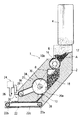
先ず、図1乃至図6により、本発明の第1実施形態を説明する。ここで、図1は正面断面図、図2は側面断面図、図3は図2の要部拡大断面図、図4はチップ部品を示す斜視図、図5は90度姿勢を変換させたチップ部品を示す斜視図、図6はチップ部品姿勢変換機構を示す斜視図である。1は、チップ部品供給装置であり、このチップ部品供給装置1は、ハウジング2を備えている。また、4は、部品収納ケース(このケースとして、例えば、日本電子機械工業会規格 EIAJ ET-7201 「表面実装部品用バルクケース」に規定されているものが使用可能である。)であり、この部品収納ケース4には、予め多数個(一般には数千〜数万個)のチップ部品Aがバラ積み状態で収納されている。ここで、チップ部品Aは、一般的には直方体形状の部品であり、例として、チップコンデンサ(例えば、長さL×幅W×厚さT=1.0mm ×0.5mm ×0.5mm の寸法を有するものがあり、日本電子機械工業会規格 EIAJ RC-2322 「電子機器用固定積層磁器チップコンデンサの標準寸法」に規定されている。)やチップ抵抗器(例えば、長さL×幅W×厚さT=1.6mm ×0.8mm ×0.45mmの寸法を有するものがあり、日本電子機械工業会規格 EIAJ RC-2130 「電子機器用チップ固定抵抗器通則」に規定されている。)がある。図4は、このチップ抵抗器(チップ部品A)を示している。ただし、チップ部品Aは、これらのものに限定されない。
【0017】
チップ部品供給装置1のハウジング2の内部の上方には、3次元的空間内にバラ積み状態のチップ部品Aを貯溜する第1部品貯溜室6が形成されており、この第1部品貯溜室6の下方には、部品厚さ方向に部品が互いに重ならない状態の2次元的空間内に多数個のチップ部品Aを貯溜する第2部品貯溜室8が形成され、さらに、この第2部品貯溜室8の下方には、部品の横断面形状に見合うように形成された空間内にチップ部品Aを1列に整列させる部品整列通路10が形成されている。
ここで、部品収納ケース4は、ハウジング2の第1部品貯溜室6の上部開口部12に装着され、これにより、部品収納ケース4内に収納された多数個のチップ部品Aが第1部品貯溜室6内に供給される。
【0018】
3次元的部品配置空間を形成する第1部品貯溜室6の底面部14は、図2に示すように、チップ部品Aが自重で滑り落ちることができる程度に傾斜して形成され、さらに、2次元的部品配置空間を形成する第2部品貯溜室8に連通している。
これらの第1部品貯溜室6と第2部品貯溜室8の間には、第1整列回転板16が設けられている。この第1整列回転板16の第1部品貯溜室6と第2部品貯溜室8に向いた一側面16a(図3参照)には、半径方向に4つの突起部16b(図1及び図3参照)が形成されている。これらの突起部16bと突起部16bに対向するハウジング2の内面との距離Bは、チップ部品Aの厚みTの値より小さく設定されている。この第1整列回転板16は、部品をその自重方向とは反対方向(上方)へ移動させるような方向へ回転する(図1においては、反時計回り)。
【0019】
また、第2部品貯溜室8の底面部18は、部品が自重で滑り落ちることができる程度に傾斜させて形成され、さらに、部品を1列に整列させる部品整列通路10に連通している。
これらの第2部品貯溜室8と部品整列通路10の間には、第2整列回転板20が設けられている。この第2整列回転板20の第2部品貯溜室8と部品整列通路10に向いた円周面20aは、摩擦力を高める材料(例えば、ゴム)や機構(例えば、ギザギザ溝)により形成され、部品をその自重方向とは反対方向(上方)へ移動させるような方向へ回転する(図1においては、反時計回り)。
【0020】
チップ部品供給装置1のハウジング2の内部の部品整列通路10の下方には、部品送り出し用のローラ装置22が設けられている。このローラ装置22は、部品整列通路10の上流側に設けられた第1ローラ22aと、下流側に設けられた第2ローラ22bと、この第1ローラ22aと第2ローラ22bを連結しチップ部品Aを搬送する部品搬送ベルト22cにより構成される。
ここで、図1に示すように、チップ部品供給装置1のチップ部品Aの供給側には、自動マウント装置24が配置されている。この自動マウント装置24の本体の下部には、チップ部品Aを受け取るためのノズル26と、チップ部品Aの供給タイミングを設定するためのアーム28がそれぞれ下方に延びるように設けられている。
【0021】
また、チップ部品供給装置1のハウジング2内部の自動マウント装置24近傍側には、図1に示すように、駆動ローラ30が設けられている。この駆動ローラ30には、上記アーム28の下降動作により図1において反時計回りに回動するレバー32が駆動機構(図示せず)を介して取り付けられている。この駆動ローラ30は、第2整列回転板20と第1駆動ベルト34により連結され、さらに、第2整列回転板20は、第1整列回転板16と第2駆動ベルト36により、ローラ装置22の第1ローラ22aと第3駆動ベルト38によりそれぞれ連結されている。ここで、駆動ローラ30の駆動機構は、レバー32の動作により駆動ローラ30が以下のように動作する機構である。即ち、アーム28の下降動動作によりレバー32が下方に向けて反時計回りに回動する。このとき、駆動ローラ30もレバー32と一体的に回動し、この結果、第1駆動ベルトが反時計回りに移動する。アーム28が上昇動作する際には、レバー32は自動的に図1に示す水平位置に戻るが、駆動ローラ30は回動することなくその位置に止まっている。
【0022】
この第1実施形態においては、上述したように、自動マウント装置24のアーム28の上下動作及びレバー32の回動動作により、駆動ローラ30を所定のタイミングで駆動させている。
しかし、この第1実施形態において、この自動マウント装置22のアーム28及びレバー32の代わりに、ハウジング2内にシリンダ機構又は薄型モータ(図示せず)を設け、これらのシリンダ機構又は薄型モータにより、駆動ローラ30を自動マウント装置24と同期させ所定のタイミングで駆動させるようにしてもよい。
【0023】
次に、このように構成された本発明の第1実施形態の動作を説明する。まず、多数個のチップ部品Aがバラ積み状態で収納されている部品収納ケース4が、チップ部品供給装置1のハウジング2の内部の上方に形成された第1部品貯溜室6の上部開口部12に装着され、これにより、部品収納ケース4内のチップ部品Aが第1部品貯溜室6内に供給される。
次に、第1部品貯溜室6の3次元空間内でバラ積み状態のままで収納されたチップ部品Aは、第1部品貯溜室6の底面部14に沿って自重により下方へ滑り落ちる。このとき、チップ部品Aがこの底面部14の下方で集合し過ぎて第2部品貯溜室8の方へ落下できなくなるときがある。しかしながら、これらのチップ部品Aは、第1整列回転板16が反時計回りに回転による一側面16aに形成された突起部16bの上方への移動により、上方に解き放たれる。この結果、解き放たれたチップ部品Aは、部品厚さ方向に互いに重ならない二次元的なバラ積み状態でスムーズに第2部品貯溜室8へ向かって自重により下方へ滑り落ちる。
ここで、この実施形態では、第1整列回転板16の一側面16aには、4つの突起部16bが形成されているが、自動マウント装置24のアーム28の上下動作が1回行われる毎に、チップ部品Aを少なくとも一度上方へ解き放つことができるような数だけこの突起部16bが設けられている。
【0024】
次に、部品は、第2部品貯溜室8内で、部品厚さ方向に互いに重ならない状態の2次元的空間内に先ず収納され、次に、底面部18に沿って自重により下方に滑り落ちる。このときは、第2部品貯溜室8の底面部18から部品整列通路10へ1列に整列して自重により滑り落ちようとする部品と第2整列回転板20の円周面20aとの間に楔状に食い込んだ部品が、第2整列回転板20の回転により生じるの円周面20aと部品との摩擦により、上方へ解き放たれる。この結果、チップ部品Aが1列で通過できる間隔が形成され、チップ部品Aは、部品整列通路10へ向かってスムーズに自重により下方へ滑り落ち、部品整列通路10上で、1列に整列する。
【0025】
一方、自動マウント装置24が下降動作することにより、ノズル26が、部品整列通路10上で1列に整列したチップ部品Aを1個づつ受け取る。
このとき、アーム28も同時に下降し、レバー32を下方へ押し下げる。このレバー32の回動動作により、駆動ローラ30が所定の角度だけ回動し、これにより、第1、第2及び第3駆動ベルト34,36,38が同時に駆動される。これにより、第1整列回転板16、第2整列回転板20及びローラ装置22は、自動マウント装置24の下降動作に同期して所定のタイミングで作動する。これにより、第1整列回転板16及び第2整列回転板20がそれぞれ所定の角度だけ反時計回りに回転する。また、ローラ装置22の第1ローラ22aも所定の角度だけ回動する。この第1ローラ22aの回動動作により、ローラ装置22の部品搬送ベルト22c上のチップ部品Aが図1の左方へ所定の距離だけ移動する。このようにして部品整列通路10上のチップ部品Aは、部品送り出し用のローラ装置22により所定のタイミングで1個づつノズル23の下方位置である所定位置に送り出される。
【0026】
上述した本発明の第1実施形態において、チップ部品Aの横断面形状が長方形の場合にはチップ部品Aの姿勢を部品供給方向に対して交差する方向に90度変換する必要が有る。図4乃至図6により、チップ部品Aの姿勢を部品供給方向に対して交差する方向に90度変換するための機構を説明する。チップ部品Aを自動マウント装置に供給する際には、直方体形状のチップ部品Aの最大面である吸着面74が上向きであることが要求される。このため、図5(a)に示された部品整列通路10へ供給されたチップ部品Aの姿勢を90度変換して図5(b)に示された姿勢(吸着面74が上向き)にする必要がある。このため、第1実施形態において、図6に示された変換溝78が形成された部品姿勢変換機構76を部品整列通路10の上流側の傾斜部に設けるようにした。この部品姿勢変換機構76は、樹脂加工品等で製作されている。この部品姿勢変換機構76により、チップ部品Aには機械的圧力が作用することなく、チップ部品Aが1列に整列した後自重により変換溝78内で滑り落ちながらその姿勢が部品供給方向に対して交差する方向に90度変換される。この結果、可動式であれば機構が複雑となり高コストとなるが、そのような問題も生じない。また、構造的に簡易であるため、機械加工が簡単で、信頼性も高い。
また、この変換溝78が形成された部品姿勢変換機構76を樹脂モールドにより製作するようにしてもよい。この場合には、複雑な機械加工が不要となる。
【0027】
次に図7乃至図15により本発明の第2実施形態を説明する。この第2実施形態は、図1に示す第1実施形態における第1整列回転板16と第2整列回転板20を設けることなく、その代わりに上下方向に往復運動をする整列板を設けるようにしたものである。
ここで、図7は正面断面図、図8は図7のC−C線に沿って見た部分断面図、図9は図7のD−D線に沿って見た部分断面図、図10は図7の第2部品貯溜室及びその周辺を示す要部拡大断面図、図11は図10を矢印Eの方向から見た部分拡大断面図、図12及び図13は整列板が上昇及び下降した状態をそれぞれ示す要部拡大断面図、図14及び図15はローラー装置の端部における部品分離機構の動作を示すための部分平面図である。
【0028】
図7乃至図9に示すように、100はチップ部品供給装置であり、このチップ部品供給装置100は、ハウジング102を備えている。また、4は部品収納ケースであり、この部品収納ケース4には、予め多数個のチップ部品Aがバラ積み状態で収納されている。
チップ部品供給装置100のハウジング102の内部の上方には、3次元的空間内にバラ積み状態のチップ部品Aを貯溜する第1部品貯溜室104が形成されており、この第1部品貯溜室104の下方には、部品厚さ方向に部品が互いに重ならない状態の2次元的空間内に多数個のチップ部品Aを貯溜する第2部品貯溜室106が形成され、さらに、この第2部品貯溜室106の下方には、部品の横断面形状に見合うように形成された空間内にチップ部品Aを1列に整列させる部品整列通路108が形成されている。
【0029】
ここで、部品収納ケース4は、ハウジング102の第1部品貯溜室104の上部開口部110に装着され、これにより、部品収納ケース4内に収納された多数個のチップ部品Aが第1部品貯溜室104内に供給される。
3次元的部品配置空間を形成する第1部品貯溜室104の底面部112は、図7及び図10に示すように、チップ部品Aが自重で滑り落ちることができる程度に傾斜して形成され、さらに、2次元的部品配置空間を形成する第2部品貯溜室106に連通している。また、第2部品貯溜室106の底面部120は、チップ部品Aが自重で滑り落ちることができる程度に傾斜させて形成され、さらに、部品を1列に整列させる部品整列通路108に連通している。
【0030】
これらの第1部品貯溜室104、第2部品貯溜室106及び部品整列通路108に連通する空間内には、上下方向に往復運動する整列板114が設けられている。この整列板114は、その上端部に第1整列部116を形成し、さらに、この第1整列部116の下方に第2整列部118を形成している。ここで、整列板114の第1整列部116は、図11に示すように、その基端部が厚みFを有し、チップ部品Aが第1部品貯溜室104から第2部品貯溜室106に向かって自重で滑り落ちる程度に傾斜した傾斜面116aが形成されている。さらに、図11に示すように、第2整列部118には、厚みがGである傾斜溝118aが形成されている。この傾斜溝118aの底部には、チップ部品Aが第1部品貯溜室104から第2部品貯溜室106に向かって自重で滑り落ちる程度に傾斜した傾斜面118bが形成されている。なお、厚みGは第2部品貯溜室106の厚みである。この結果、整列板114の第2整列部118の傾斜溝118aは、上下移動すると共に第2部品貯溜室106の一部として機能している。
【0031】
この整列板114は、所定のタイミングで図10と図13に示す最下位置と図14に示す最上位置との間を上下移動し、チップ部品Aを、後述するように、第1部品貯溜室104から第2部品貯溜室106を経由して部品整列通路108に導く。
この第2実施形態においては、第1整列部116と第2整列部118とが整列板114として一体的に形成されているが、本発明は、これに限らず、第1整列部116と第2整列部118とを別々の整列板にそれぞれ形成するようにしてもよい。
【0032】
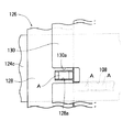
チップ部品供給装置100のハウジング102の内部の部品整列通路108の上流側には、図6に示す部品姿勢変換機構76と同様な機能を有する部品姿勢変換機構122が設けられ、この反転機構122により、チップ部品Aの姿勢が、その吸着面が上向きとなるように部品供給方向に対して交差する方向に90度変換される。
また、部品整列通路108の下流側には、部品送り出し用のローラ装置124が設けられている。このローラ装置124は、図7において右側に設けられた従動ローラ124aと、左側に設けられた駆動ローラ124bと、この従動ローラ124aと駆動ローラ124bを連結しチップ部品Aを搬送する部品搬送ベルト124cにより構成される。
【0033】
さらに、図14と図15に示すように、ローラ装置124の部品搬送ベルト124cの先端部には、チップ部品Aを1つづつ分離して所定のタイミングで外部へ送りだす部品分離機構126が設けられている。この部品分離機構126は、部品搬送ベルト124cによって送られて来たチップ部品Aをベルト124cの先端部で止めるストッパー部材128とチップ部品Aの部品整列通路108からの飛び出しを防ぐ上部カバー部材130から構成されている。ストッパー部材128には、チップ部品Aが丁度1つ入ることが可能な大きさの溝部128aが形成されている。このストッパー部材128は、部品進行方向Iと90度交差する水平方向Jに移動可能である。また、上部カバー部材130には、ストッパー部材128が水平移動した位置(図15に示す位置)でチップ部品Aを取り出すことができる大きさの窓部130aが形成されており、この窓部130aからチップ部品Aを外部へ取り出すことができるようになっている。ここで、図14はストッパー部材128がチップ部品Aを受け入れる状態の位置を示し、図15はチップ部品を取り出す状態の位置を示している。
【0034】
図7に示すように、チップ部品供給装置100のチップ部品Aの供給側には、自動マウント装置24が配置されている。この自動マウント装置24の本体の下部には、チップ部品Aを受け取るためのノズル26が設けられている。
なお、駆動ローラ124b、整列板114及びストッパー部材128は、1つの駆動源(図示せず)に接続されている。駆動源として、ハウジング102内に内蔵された内部駆動(例えば、モーター、エアーシリンダ等)が使用される。この駆動源により、駆動ローラ124b、整列板114及びストッパー部材128が、自動マウント装置24の部品の取り出しのための上下動作と所定のタイミングで同期して駆動され、この結果、この所定のタイミングで外部へチップ部品Aが送り出される。
【0035】
次にこのように構成された第2実施形態の動作を説明する。まず、多数個のチップ部品Aがバラ積み状態で収納されている部品収納ケース4が、チップ部品供給装置100のハウジング102の内部の上方に形成された第1部品貯溜室104の上部開口部110に装着され、これにより、部品収納ケース4内のチップ部品Aが第1部品貯溜室104内に供給される。
【0036】
次に、第1部品貯溜室104の3次元空間内でバラ積み状態のままで収納されたチップ部品Aは、第1部品貯溜室104の底面部112に沿って自重により下方へ滑り落ちる。チップ部品Aの幾つかは、第1部品貯溜室104からスムーズに直接第2部品貯溜室106に落下する。このとき、図10に示すように、第1部品貯溜室104の底面部112の下方で、整列して自重により滑り落ちようとする部品と整列板114の第1整列部116の傾斜面116aから滑り落ちようとする部品が集中し過ぎて楔状に食い込み、整列した部品が第2部品貯溜室106へ落下できなくなることがある。しかしながら、本実施形態においては、図12に示すように、整列板114の第1整列部116が上方に移動するため、この第1整列部116の傾斜面116aから滑り落ちようとする部品が上方に解き放たれ、これれにより、楔状の食い込みが解消される。このとき、チップ部品Aは、再び整列し、部品の厚さ方向に互いに重ならない2次元的なバラ積み状態でスムーズに第2整列部118の傾斜溝118aを通って第2部品貯溜室106へ向かって自重により下方へ滑り落ちる。このようにして、チップ部品Aは、第2部品貯溜室106内で、部品の厚さ方向に互いに重なり合わない状態で2次元形空間に収納される。この後、図13に示すように、整列板114の第1整列部116が下方に移動し、同様な動作が所定のタイミングで繰り返される。
【0037】
このようにして第2部品貯溜室106内に収納されたチップ部品Aは、第2部品貯溜室106の底面部120に沿って自重により下方へ滑り落ちる。このとき、図10に示すように、第2部品貯溜室106の底面部120の下方で、整列して自重により滑り落ちようとする部品と整列板114の第2整列部118の傾斜溝118aから滑り落ちようとする部品が集中し過ぎて楔状に食い込み、整列した部品が部品整列通路108へ落下できなくなることがある。しかしながら、本実施形態においては、図12に示すように、整列板114の第2整列部118が上方に移動するため、この第2整列部118の傾斜溝118aから滑り落ちようとする部品が上方に解き放たれ、これにより、楔状の食い込みが解消される。このとき、チップ部品Aは、再び整列し、スムーズに部品整列通路108の方に滑り落ちる。この後、図13に示すように、整列板114の第2整列部118が下方に移動し、同様な動作が所定のタイミングで繰り返される。
【0038】
このようにして部品整列通路108へ導かれたチップ部品Aは、自重で部品姿勢変換機構122内に滑り落ち、その姿勢が90度反転された後、部品送り出し用ローラ装置124へ導かれる。ローラ装置124の部品搬送ベルト124cにより搬送されたチップ部品Aは、ストッパー部材128の溝部128aに当接して停止する(図14参照)。このとき、停止したチップ部品Aと後続のチップ部品Aは、部品搬送ベルト124c上で滑っている状態となる。
このようにしてストッパー部材128の溝部128aが確実にチップ部品Aを受け止めた後、このストッパー部材128は、図15に示すように、部品搬送ベルト124cの部品搬送方向とは90度交差した方向に所定の距離だけ水平移動する。このストッパー部材128の水平移動により、チップ部品Aは後続のチップ部品Aから分離されるため、後続のチップ部品Aにより溝部128aのチップ部品Aが押し付けられていた力が解除され、この結果、チップ部品Aの取り出しが容易となる。
【0039】
また、上部カバー部材130が設けられているので、チップ部品Aの飛び出しが防止される。上部カバー部材130に形成された窓部130aから、自動マウント装置24のノズル26により、チップ部品Aが1個づつ外部へ取り出される。
この実施形態では、整列板114、駆動ローラ124b及びストッパー部材128は、所定のタイミングで連動同期して1つの駆動源により駆動される。
【0040】
次に図16乃至図20により本発明の第3実施形態を説明する。図16は正面断面図、図17は図16のK−K線に沿って見た部分断面図、図18は図16のM−M線に沿って見た部分断面図である。図19は、ローラー装置の端部における部品分離機構の動作(部品受取り位置)を示すための部分平面図であり、図20は、ローラー装置の端部における部品分離機構の動作(部品取出し位置)を示すための部分平面図である。この第3実施形態において、上述した第2実施形態と同一構成のものは、同一符合を付し、その説明は省略する。
この本発明の第3実施形態は、第2実施形態における部品収納ケース4、第1部品貯溜室104、第2部品貯溜室106、部品整列通路108と同様な構造のものをチップ部品供給装置の表側(右側)と裏側(左側)にそれぞれ設けると共に、ハウジング、整列板、ローラ装置及び部品分離機構は共用して使用するようにしたものである。
【0041】
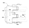
即ち、本発明の第3実施形態のチップ部品供給装置150は、ハウジング152を備え、このハウジング152内に、部品収納ケース4、第1部品貯溜室104、第2部品貯溜室106、部品整列通路108が、平面的に見て左右点対称となるように(図18参照)、チップ部品供給装置150の表側と裏側にそれぞれ設けられている。
また、ハウジング152には、整列板154が設けられており、この整列板154は、表裏対称(左右点対称)な形状であり、表側と裏側に、第2実施形態の整列板114ものと同様な構造の第1整列部と第2整列部をそれぞれ備えている。
また、部品分離機構158は、ストッパー部材160と上部カバー部材162により構成されている。ストッパー部材160には、2つの部品整列通路108に対応するように、2つの溝部160aが設けられており、同様に、上部カバー部材162には、2つの窓部162aが設けられている。ここで、図19はストッパー部材160がチップ部品Aを受け入れる状態の位置を示し、図20はチップ部品を取り出す状態の位置を示している。
【0042】
さらに、図16に示すように、ローラ装置156が設けられている。この第3実施形態におけるローラ装置156は、自動マウント装置24のアーム28の上下動作により、所定のタイミングで駆動動作を行う構造を採用している。即ち、ローラ装置156は、部品供給方向に対して上流側と下流側に設けられたローラー130,131、これらのローラ130,131を連結する部品搬送ベルト132、自動マウント装置24のアーム28にその一端が押し下げられて上下動する第1レバー133、この第1レバー133の他端にその一端が連結された第2レバー134と、この第2レバー134の他端に連結され回動動作を行う第1回転盤135と、この第1回転盤135にその一端が連結された第3レバー136と、この第3レバー136の他端にその一端が係合し且つその他端が上述した整列板154の下端部に連結されたL字形状の第4レバー137と、第1回転盤135にその一端が連結され且つその他端がローラ131の回転軸と連結された第5レバー138と、ローラ131を一方向(反時計回り)のみに回転可能とするラッチ139と、第1回転盤135にその一端が連結された第6レバー140と、この第6レバー140の他端に連結され回動動作を行い且つストッパ作動部材141aを備えた第2回転盤141と、第1レバー133の他端(図16において右側端)を常時下方に押し下げるように付勢された第1バネ142と、整列板154が最上位置に位置するように第4レバー137の一端(下側端)を図16中左側に引っ張る第2バネ143と、第2回転盤141を時計回りに回動するように常時付勢された第3バネ144と、から構成されている。
【0043】
次に、このように構成された第3実施形態の動作を説明する。自動マウント装置24が図16に示すように上方に位置しているときは、整列板154は最上位置に位置している。自動マウント装置24が下降すると、自動マウント装置24のアーム28も同時に下降動作し、これにより、第1レバー133、第2レバー134、第1回転盤135、第3レバー136、第4レバー137を介して、整列板154が最下位置に向けて下降する。このとき、第5レバー138が図16中左方向に移動するが、ローラ131はラッチ139により係止されているため時計回りには回転しないようになっている。同時に、第6レバー140が反時計回りに回動し、その結果、第2回転盤141が時計回りに回転し、ストッパ作動部材141aがストッパー部材160を水平方向に移動させる。これにより、ストッパー部材160は図20に示す位置となる。また、自動マウント装置24と共にノズル26も下降し、ノズル26がチップ部品Aを外部に取り出す。この後、自動マウント装置24は上昇する。このとき、第1バネ142、第2バネ143及び第3バネ144の作用により、ローラ装置156は、図16に示した位置に復帰する。また、この自動マウント装置24の上昇により、第5レバー138が図16中右側に移動する。この結果、ローラ131が反時計回りに所定距離だけ駆動され、部品搬送ベルト132が反時計回りの方向に所定距離だけチップ部品Aを搬送する。
このようにして、所定のタイミングで整列板が上下移動を行うことにより、第2実施形態と同様に、別々の部品収納ケース4に収納されたチップ部品Aは、それぞれの側の第1部品貯溜室104から第2部品貯溜室106を経由して部品整列通路108に同期進行の形で導かれる。ローラー装置156の部品搬送ベルト132上の2つの部品整列通路108により導かれたそれぞれのチップ部品Aは、ストッパー部材160の溝部160aにそれぞれ収納され、その後、ストッパ部材160が水平移動し、上部カバー部材162の窓部162aから、自動マウント装置24のノズル26により1個づつ外部へ取り出される。
【0044】
この第3実施形態によれば、このようにハウジング152、整列板154、ローラ装置156及び部品分離機構158を共有とすることにより、コストを押さえることができ、しかも、2つの部品整列通路108を設けたため、部品供給能力は2倍となる。さらに、2つの部品整列通路108を設けたにもかかわらず、部品搬送ベルト132は1つの部品整列通路を設けた第2実施形態の部品搬送ベルト124cと同様な幅のものを使用できる。このようにして、薄型で高密度な部品供給装置を提供することができる。
【0045】
次に図21により本発明の第4実施形態を説明する。この第4実施形態において、図7乃至図15に示された第2実施形態と同一構成のものは同一符号を付し、その説明は省略する。
図21に示すように、170は、チップ部品供給装置であり、このチップ部品供給装置170は、ハウジング172を備えている。また、54は、カートリッジ式部品収納ケースであり、この部品収納ケース54には、予め多数個(一般には数千〜数万個)のチップ部品Aが収納されている。このカートリッジ式部品収納ケース54には、部品厚さ方向には部品が重ならない2次元的部品配置空間が形成されている。このため、表裏判別する必要のある部品の場合には、この2次元空間内に、表裏判別し表裏整列させた(チップ部品の裏側と表側がそれぞれ同一方向に向くように整列させた)状態でチップ部品Aを収納するようにすればよい。
チップ部品供給装置170のハウジング172の内部の上方には、部品厚さ方向に部品が互いに重ならない状態の2次元的空間内に多数個のチップ部品Aを表裏反転しないようにして貯溜する部品貯溜室174が形成され、さらに、この部品貯溜室56の下方には、部品の横断面形状に見合うように形成された空間内にチップ部品Aを1列に整列させる部品整列通路108が形成されている。
【0046】
ここで、カートリッジ式部品収納ケース54は、ハウジング172の部品貯溜室174の上部開口部176に斜めに傾けて装着され、これにより、カートリッジ式部品収納ケース54内に収納された多数個のチップ部品Aが部品貯溜室174内に2次元的に整列したままの状態で供給される。
部品貯溜室174の底面部178は、部品が自重で滑り落ちることができる程度に傾斜させて形成され、さらに、チップ部品Aを1列に整列させる部品整列通路108に連通している。
これらの部品貯溜室174と部品整列通路108の間には、上下移動可能な整列板180が設けられている。この整列板180は、部品貯溜室174と同じ厚み(図11のGと同じ厚み)を有し、その上端部には、傾斜面180aが形成されている。なお、図21は、この整列板180が上昇した位置にある状態を示している。
さらに、第2実施形態と同様に、部品姿勢変換機構122、ローラー装置124、部品分離機構126等が設けられている。
【0047】
このように構成された本発明の第4実施形態の動作を説明する。まず、多数個のチップ部品Aが2次元状態(場合によっては、表裏判別し表裏整列させた状態)で収納されているカートリッジ式部品収納ケース54が、チップ部品供給装置170のハウジング172の内部の上方に形成された部品貯溜室174の上部開口部176に装着され、これにより、カートリッジ式部品収納ケース54内のチップAが2次元状態(場合によっては、表裏判別された状態)のままで部品貯溜室174内に供給される。
次に、部品は、部品貯溜室174内で、部品厚さ方向に互いに重ならない状態の二次元的空間内に先ず収納され、次に、底面部178に沿って自重により下方に滑り落ちる。このときは、部品貯溜室174の底面部178の下方で、整列して自重により滑り落ちようとする部品と整列板180の傾斜面180aから滑り落ちようとする部品が集中し過ぎて楔状に食い込み、整列した部品が部品整列通路108へ落下できなくなる。しかしながら、本実施形態においては、整列板180の傾斜面180aが上方に移動するため、整列板180の傾斜面180aから滑り落ちようとする部品が上方に解き放たれ、これにより、楔状の食い込みが解消される。このとき、チップ部品Aは、再び整列し、スムーズに部品整列通路108の方に滑り落ちる。この後、整列板180の傾斜面180aが下方に移動し、同様な動作が所定のタイミングで繰り返される。
【0048】
このようにして部品整列通路108へ導かれたチップ部品Aは、第2実施形態と同様に、部品姿勢変換機構122、ローラ装置124、ストッパー部材128の溝部128aを経由して、上部カバー部材130に形成された窓部130aから、自動マウント装置24のノズル26により、チップ部品Aが1個づつ外部へ取り出される。
【0049】
次に図22により本発明の第5実施形態を説明する。図22(a)は、図11に相当する図面であり、チップ部品供給装置を示す部分拡大断面図であり、図22(b)は、図22(a)の整列板をN−N方向から見た部分断面図である。
この第5実施形態においては、ハウジング200が、本体部202と、裏カバー204と、表カバー206から構成されている。このハウジング200の本体部202には、図7等で示される第2実施形態と同様に、第1部品貯溜室104及び第2部品貯溜室106が形成されている。
この第5実施形態においては、ハウジング200の本体部202に傾斜面202a(固定)が形成されている。
また、ハウジング200の表カバー206内にも同様に傾斜面206a(固定)が形成されている。さらに、この表カバー206内には、第1部品貯溜室104の一部として機能する窪み部104aが形成されている。
210は整列板であり、この整列板210は、第1整列部212と第2整列部214と備えている。第1整列部212には、整列板210が下方に位置しているとき(図中実線で示す)、ハウジング200の本体部202の傾斜面202aと連続するような傾斜面212aが形成されている。また、この整列板210の第1整列部212は、表カバー206の内部にも形成され、同様に、傾斜面212bが形成されている。この傾斜面212bは、それが下方に位置しているとき表カバー206の内部に設けられた傾斜面206aと連続するように形成されている。整列板210の第2整列部214には、図7等に示す第2実施形態と同様に、傾斜溝214aが形成され、この傾斜溝214aの底部には、チップ部品が第2部品貯溜室106から部品整列通路に向かって自重で滑り落ちる程度に傾斜した傾斜面214bが形成されている。図22中、仮想線は、整列板210が上方に移動した位置を示している。
【0050】
この第5実施形態によれば、チップ部品を第1部品貯溜室104から第2部品貯溜室106に導く際、整列板210の第1整列部212が上方に移動することにより、第1部品貯溜室104内での部品の楔状の食い込みが解消され、チップ部品Aは、第2整列部214の傾斜溝214aを通って第2部品貯溜室106に向かって自重により下方に滑り落ちる。また、整列板210の第2整列部214が上方に移動することにより、第2部品貯溜室106内での部品の楔状の食い込みが解消され、チップ部品Aは、スムーズに部品整列通路の方に滑り落ちる。
一方、図11に示す第2実施形態では、チップ部品の大きさや形状・材質によっては、整列板114を上昇させる際に、第1整列部116の傾斜面116aとハウジング120の表カバー(図11において傾斜面116aの右側に位置している)の内側壁面との間で、チップ部品が挟まり、このチップ部品により表カバーの内側壁面が損傷することがある。このような場合において、この第5実施形態によれば、この表カバー206内に窪み部104aを形成するようにしているので、整列板210が上昇する際に、上述したようなチップ部品による表カバーの内側壁面の損傷を確実に防止することができる。
なお、この図22に示された第5実施形態の構造は、図16乃至図20に示された第3実施形態に適用可能である。
【0051】
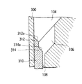
次に図23及び図24により本発明の第6実施形態を説明する。この第6実施形態は、図22に示された第5実施例における整列板210をよりシンプルな形状としたものである。ここで、図23は、図11及び図22に相当する図面であり、チップ部品供給装置を示す部分拡大断面図であり、図24は、図23のP−P方向から見たチップ部品供給装置の部分断面図である。
この第6実施形態においては、ハウジング300が、本体部302と、裏カバー304と、表カバー306から構成されている。このハウジング300の本体部302には、第1部品貯溜室104及び第2部品貯溜室106が形成されている。ハウジング300の本体部302の底面に傾斜面302a(固定)が形成されている。
また、ハウジング300の表カバー306内にも同様に傾斜面306a(固定)が形成されている。さらに、この表カバー306内には、第1部品貯溜室104の一部として機能する窪み部104aが形成されている。
310は整列板であり、この整列板310は、その上端部に第1整列部312を備え、さらに、この第1整列部312の下方に第2整列部314を備えている。この第1整列部312には、第1部品貯溜室104と第2部品貯溜室106の間に位置する傾斜面312aが形成されている。また、第2整列部314には、第2部品貯溜室106と部品整列通路108の間に位置する傾斜面314aが形成されている。整列板310の厚みは、第2部品貯溜室106と同じである。この整列板310は、所定の最上位置(図24に示す位置)と所定の最下位置との間を上下移動可能である。これらの最上位置と最下位置は任意に変更可能である。
【0052】
この第6実施形態によれば、チップ部品を第1部品貯溜室104から第2部品貯溜室106に導く際、図24で示すように、整列板310の第1整列部312が上方に移動することにより、第1部品貯溜室104の下部で生じる部品の楔状の食い込みが解消され、チップ部品Aは、第2部品貯溜室106に向かって自重により下方に滑り落ちる。また、整列板310の第2整列部314が、上方に移動することにより、第2部品貯溜室106内での部品の楔状の食い込みが同様に解消され、チップ部品Aは、スムーズに部品整列通路108の方に自重により滑り落ちる。
さらに、この第6実施形態によれば、図22に示す第5実施形態と同様に、表カバー306内に窪み部104aを形成するようにしているので、整列板310が上昇する際に、チップ部品による表カバーの内側壁面の損傷を確実に防止することができる。
同様に、図23及び図24に示された第6実施形態の構造は、図16乃至図20に示された第3実施形態に適用可能である。
【0053】
以上、第1整列手段、第2整列手段及び整列手段として、回転板又は整列板を使用した実施形態を説明したが、本発明は、これに限定されることはない。即ち、本発明の第1整列手段、第2整列手段及び整列手段として、上述の回転板又は整列板以外に、振動式(ボウル型、直進型及びホッパ型)、回転式(ドラム型及び水平型)、揺動式(ブレード揺動型及びホッパ揺動型)、ベルト式(エスカレータ型及び水平型)、ジェット式(液体型及び空気型)等の既存の機構を用いることも可能である。
【0054】
【発明の効果】
以上説明したように、本発明のチップ部品供給装置によれば、バラ積み供給方式でチップ部品を確実且つ効率的に供給することができる。また、構造が比較的簡単で低コストで大量に部品を供給することができる。さらに、本発明のカートリッジ式部品収納ケースによれば、2次元的部品配置空間内でチップ部品を表裏整列させて収納することができる。
【図面の簡単な説明】
【図1】 本発明のチップ部品供給装置の第1実施形態を示す正面断面図
【図2】 図1の側面断面図
【図3】 図2の要部拡大断面図
【図4】 チップ部品を示す斜視図
【図5】 90度姿勢を変換されたチップ部品を示す斜視図
【図6】 チップ部品姿勢変換機構を示す斜視図
【図7】 本発明のチップ部品供給装置の第2実施形態を示す正面断面図
【図8】 図7のC−C線に沿って見た部分断面図
【図9】 図7のD−D線に沿って見た部分断面図
【図10】 図7の第2部品貯溜室及びその周辺を示す要部拡大断面図
【図11】 図10を矢印Eの方向から見た部分拡大断面図
【図12】 整列板が上昇及び下降した状態を示す腰部拡大断面図
【図13】 整列板が下降した状態を示す腰部拡大断面図
【図14】 ローラー装置の端部における部品分離機構の動作(部品受取り位置)を示すための部分平面図
【図15】 ローラー装置の端部における部品分離機構の動作(部品取出し位置)を示すための部分平面図
【図16】 本発明のチップ部品供給装置の第3実施形態を示す正面断面図
【図17】 図16のK−K線に沿って見た部分断面図
【図18】 図16のM−M線に沿って見た部分断面図
【図19】 ローラー装置の端部における部品分離機構の動作(部品受取り位置)を示すための部分平面図
【図20】 ローラー装置の端部における部品分離機構の動作(部品取出し位置)を示すための部分平面図
【図21】 本発明のチップ部品供給装置の第4実施形態及び本発明のカートリッジ式部品収納ケースを示す正面断面図
【図22】 本発明のチップ部品供給装置の第5実施形態を示す正面断面図(図22(a))及びN−N方向から見た部分断面図(図22(b))
【図23】 本発明のチップ部品供給装置の第6実施形態を示す部分拡大断面図
【図24】 図23のP−P方向から見たチップ部品供給装置の部分断面図
【符号の説明】
1,100,150,170 チップ部品供給装置
2,102,152,172,200 ハウジング
4,54 部品収納ケース
6,104 第1部品貯溜室
8,106 第2部品貯溜室
10,58,108 部品整列通路
12,60,110,174 上部開口部
14,62,120,178 底面部
16 第1整列回転板
18 底面部
20 第2整列回転板
22,124,156 ローラ装置
24 自動マウント装置
26 ノズル
28 アーム
30 駆動ローラ
32 レバー
34 第1駆動ベルト
36 第2駆動ベルト
38 第3駆動ベルト
56,174 部品貯溜室
64 整列回転板
72 駆動レバー装置
74 吸着面
76,122 部品姿勢変換機構
78 変換溝
114,154,180,210,310 整列板
116,212 第1整列部
118,214 第2整列部
126 部品分離機構
128,160 ストッパー部材
130,162 上部カバー部材
312 傾斜部[0001]
BACKGROUND OF THE INVENTION
The present invention relates to a chip component supply device and a cartridge-type component storage case, and in particular, is used for a component supply device that supplies bulk components arranged in a row and supplies such a chip component supply device. The present invention relates to a cartridge type component storage case. The chip component supply device and the cartridge-type component storage case of the present invention can be used, for example, in a component supply unit of an automatic mounting device for mounting a chip-type electronic component.
[0002]
[Prior art]
An extremely wide variety of chip components are mounted on the printed circuit board. At this time, an automatic mounting apparatus is used to transport and mount the chip components on the printed circuit board. In order to supply the chip component to the automatic mounting device, a chip component supply device is required. The chip component supply device is roughly classified into a vibration type, a rotary type, a swing type, a belt type, and the like, and the vibration type is most frequently used conventionally.
[0003]
As another example, a chip alignment / separation apparatus described in, for example, Japanese Patent Application Laid-Open No. 62-280129 is known. The chip alignment / separation apparatus described in this publication includes a chip storage chamber for storing a large number of chips stacked in bulk, so that the chip components can move to the lower part of the storage chamber under their own weight. In addition, the inner peripheral surface is inclined downward, or the chip storage chamber itself is inclined downward. The tip storage chamber is connected to the tip alignment hole at the lower end thereof, and further, an air outlet for intermittently ejecting air is provided in the vicinity of the installation location. The chips accumulated in the lower part of the chip storage chamber are blown up by the air blown out from the air outlet, then fall down by their own weight, and enter the inlets of the chip alignment holes. The chip alignment holes are formed in accordance with the shape of the chip, and only one chip can enter, so the chips are aligned one by one in the chip alignment hole. Thereafter, by pulling out the chips one by one from the chip alignment holes by appropriate means, it is possible to take out the chips that are in a stacked state one by one.
[0004]
As another example, a storage case for electronic components described in Japanese Patent Publication No. 7-48596 is known. In the electronic component storage case described in this publication, a chip component storage path is provided in a spiral shape in a case body, and chip components are supplied in a state of being packed in advance along the storage path.
[0005]
[Problems to be solved by the invention]
However, in the chip alignment / separation apparatus described in Japanese Patent Application Laid-Open No. 62-280129, whether or not the chip successfully enters the alignment hole depends on the falling posture of the chip that is blown off and dropped into a three-dimensional space. It depends heavily. For this reason, the probability that the chip does not enter the chip alignment hole is too large to be ignored. For this reason, it is difficult to reliably and efficiently enter the chip into the alignment hole. In addition, for parts that require front / back discrimination, it is necessary to discriminate after the chip enters the chip alignment hole, and then turn over, and the supply speed of the part is reduced accordingly. In addition, the structure of the apparatus is complicated, which is a factor that increases costs.
[0006]
On the other hand, in the electronic component storage case described in Japanese Examined Patent Publication No. 7-48596, chip parts can be stored in a state where the front and back surfaces are aligned. There is a problem that it is necessary to form it with high accuracy in accordance with the shape of the parts, and various types of storage cases are required, resulting in high costs. In addition, the number of chip components stored is limited to the length of the spiral passage, and there is a problem that a large amount of components cannot be supplied.
[0007]
Accordingly, the present invention has been made to solve the above-described problems of the prior art, and provides a chip component supply device that can reliably and efficiently supply chip components by a bulk supply method. It is aimed.
Another object of the present invention is to provide a chip component supply apparatus that can supply a large amount of components at a low cost with a relatively simple structure.
Another object of the present invention is to provide a chip component supply device that supplies chip components by storing the chip components in a front-and-back arrangement.
It is another object of the present invention to provide a cartridge type component storage case that can store chip components in a front-and-back arrangement and is detachable from a chip component supply device.
[0008]
[Means for Solving the Problems]
In order to achieve the above object, a chip component supply apparatus according to the present invention is provided with a first component storage chamber for storing chip components in a stacked state, and in communication with the first component storage chamber. Are disposed in a space formed so as not to overlap each other in the thickness direction, a second component storage chamber for two-dimensionally storing the chip components, and a cross section of the chip component provided at the lower portion of the second component storage chamber. A component alignment passage formed to match the shape and arranged in one row for chip components, and provided between the first component storage chamber and the second component storage chamber, and the chip components are two-dimensionally aligned to form a first one. A first aligning / rotating means for moving from the one-part storage chamber to the second-part storage chamber; and a second-part storage chamber provided between the second-part storage chamber and the part-alignment passage to align the chip parts one-dimensionally. Second alignment to move from one to the part alignment passage And the rolling means is characterized by having a delivery means for feeding the chip components on the component alignment path to one at a predetermined position.
[0009]
In the present invention configured as described above, the chip parts stored in a bulk state in the first part storage chamber are moved to the second part storage chamber so that the chip parts do not overlap each other in the thickness direction. In the formed space, the chip parts are stored two-dimensionally, and finally, the chip parts are aligned in a row in the part alignment path. In this way, the chip parts are transferred from the stacked state (three dimensions) to one row (two dimensions) via the two dimensions, so that the chip parts can be supplied efficiently. . At that time, the first alignment rotation means and the second alignment rotation means can be used to reliably shift from three dimensions to two dimensions and from two dimensions to one column (one dimension).
[0010]
In the present invention, preferably, the component alignment passage has a component posture changing mechanism for changing the posture of the chip component by a predetermined angle.
[0011]
In the present invention, preferably, the first aligning / rotating means is First parts storage room When Second part storage room And a second aligning / rotating means having a second aligning / rotating plate rotating in the space between the second component storage chamber and the component aligning passage.
[0012]
In the present invention, preferably, the first component storage chamber has a bottom surface formed so as to be inclined so that the chip component can move downward by its own weight, and the second component storage chamber has the chip component downward by its own weight. It has a bottom surface portion that is inclined so that it can move.
[0013]
In the present invention, preferably, each of the first part storage chamber, the second part storage chamber, and the part alignment passage is provided.
[0014]
The present invention preferably further includes a single driving means for driving the first aligning and rotating means, the second aligning and rotating means, and the delivery means.
[0016]
DETAILED DESCRIPTION OF THE INVENTION
Embodiments of the present invention will be described below with reference to the accompanying drawings.
First, a first embodiment of the present invention will be described with reference to FIGS. Here, FIG. 1 is a front sectional view, FIG. 2 is a side sectional view, FIG. 3 is an enlarged sectional view of a main part of FIG. 2, FIG. 4 is a perspective view showing a chip component, and FIG. FIG. 6 is a perspective view showing a chip part posture changing mechanism.
[0017]
Above the inside of the
Here, the component storage case 4 is mounted in the
[0018]
As shown in FIG. 2, the
Between the first
[0019]
Further, the
A second
[0020]
Below the
Here, as shown in FIG. 1, an
[0021]
Further, as shown in FIG. 1, a driving
[0022]
In the first embodiment, as described above, the driving
However, in this first embodiment, instead of the
[0023]
Next, the operation of the first embodiment of the present invention configured as described above will be described. First, a component storage case 4 in which a large number of chip components A are stored in a stacked state is an
Next, the chip component A stored in the three-dimensional space of the first
Here, in this embodiment, four
[0024]
Next, the components are first stored in a two-dimensional space in the second
[0025]
On the other hand, when the
At this time, the
[0026]
In the first embodiment of the present invention described above, when the cross-sectional shape of the chip component A is rectangular, it is necessary to convert the attitude of the chip component A by 90 degrees in a direction intersecting the component supply direction. A mechanism for converting the posture of the chip component A by 90 degrees in a direction intersecting the component supply direction will be described with reference to FIGS. When supplying the chip component A to the automatic mounting apparatus, the
Further, the component
[0027]
Next, a second embodiment of the present invention will be described with reference to FIGS. In the second embodiment, the first
7 is a front sectional view, FIG. 8 is a partial sectional view taken along line CC in FIG. 7, FIG. 9 is a partial sectional view seen along line DD in FIG. 7 is an enlarged cross-sectional view of a main part showing the second component storage chamber and its periphery in FIG. 7, FIG. 11 is a partially enlarged cross-sectional view of FIG. 10 viewed from the direction of arrow E, and FIGS. FIG. 14 and FIG. 15 are partial plan views for illustrating the operation of the component separating mechanism at the end of the roller device.
[0028]
As shown in FIGS. 7 to 9,
Above the interior of the
[0029]
Here, the component storage case 4 is mounted in the
As shown in FIGS. 7 and 10, the
[0030]
In a space communicating with the first
[0031]
The
In the second embodiment, the
[0032]
A component
Further, a
[0033]
Further, as shown in FIGS. 14 and 15, a
[0034]
As shown in FIG. 7, the
The
[0035]
Next, the operation of the second embodiment configured as described above will be described. First, the component storage case 4 in which a large number of chip components A are stored in a stacked state is an
[0036]
Next, the chip component A stored in the three-dimensional space of the first
[0037]
The chip component A housed in the second
[0038]
The chip component A guided to the
After the
[0039]
Further, since the
In this embodiment, the
[0040]
Next, a third embodiment of the present invention will be described with reference to FIGS. 16 is a front sectional view, FIG. 17 is a partial sectional view taken along line KK in FIG. 16, and FIG. 18 is a partial sectional view seen along line MM in FIG. FIG. 19 is a partial plan view for illustrating the operation (component receiving position) of the component separation mechanism at the end of the roller device, and FIG. 20 is the operation (component extraction position) of the component separation mechanism at the end of the roller device. It is a fragmentary top view for showing. In this 3rd Embodiment, the thing of the same structure as 2nd Embodiment mentioned above attaches | subjects the same code | symbol, and abbreviate | omits the description.
The third embodiment of the present invention has the same structure as the component storage case 4, the first
[0041]
That is, the chip
The
The
[0042]
Furthermore, as shown in FIG. 16, a
[0043]
Next, the operation of the third embodiment configured as described above will be described. When the
In this manner, the alignment plate moves up and down at a predetermined timing, so that the chip components A stored in the separate component storage cases 4 are stored in the first component storage on the respective sides as in the second embodiment. The
[0044]
According to the third embodiment, since the
[0045]
Next, a fourth embodiment of the present invention will be described with reference to FIG. In the fourth embodiment, the same components as those of the second embodiment shown in FIGS. 7 to 15 are denoted by the same reference numerals, and the description thereof is omitted.
As shown in FIG. 21,
In the upper part of the
[0046]
Here, the cartridge type
The
An
Further, as in the second embodiment, a component
[0047]
The operation of the fourth embodiment of the present invention configured as described above will be described. First, a cartridge type
Next, the components are first accommodated in the two-dimensional space in the
[0048]
In this way, the chip part A guided to the
[0049]
Next, a fifth embodiment of the present invention will be described with reference to FIG. FIG. 22A is a diagram corresponding to FIG. 11 and is a partially enlarged sectional view showing the chip component supply device. FIG. 22B is a diagram illustrating the alignment plate of FIG. FIG.
In the fifth embodiment, the
In the fifth embodiment, an
An inclined surface 206a (fixed) is similarly formed in the
[0050]
According to the fifth embodiment, when the chip component is guided from the first
On the other hand, in the second embodiment shown in FIG. 11, depending on the size, shape and material of the chip component, when the
The structure of the fifth embodiment shown in FIG. 22 is applicable to the third embodiment shown in FIGS.
[0051]
Next, a sixth embodiment of the present invention will be described with reference to FIGS. In the sixth embodiment, the
In the sixth embodiment, the
An
[0052]
According to the sixth embodiment, when the chip component is guided from the first
Furthermore, according to the sixth embodiment, as in the fifth embodiment shown in FIG. 22, the
Similarly, the structure of the sixth embodiment shown in FIGS. 23 and 24 is applicable to the third embodiment shown in FIGS.
[0053]
The embodiment using the rotating plate or the alignment plate as the first alignment unit, the second alignment unit, and the alignment unit has been described above, but the present invention is not limited to this. That is, as the first aligning means, the second aligning means, and the aligning means of the present invention, in addition to the rotating plate or the aligning plate described above, a vibration type (bowl type, straight type and hopper type), a rotary type (drum type and horizontal type) ), Swing type (blade swing type and hopper swing type), belt type (escalator type and horizontal type), jet type (liquid type and air type), and the like can also be used.
[0054]
【The invention's effect】
As described above, according to the chip component supply apparatus of the present invention, chip components can be reliably and efficiently supplied by the bulk supply method. In addition, the structure is relatively simple and a large amount of parts can be supplied at low cost. Furthermore, according to the cartridge-type component storage case of the present invention, chip components can be stored in a two-dimensional component placement space with the front and back aligned.
[Brief description of the drawings]
FIG. 1 is a front sectional view showing a first embodiment of a chip component supply apparatus according to the present invention.
FIG. 2 is a side sectional view of FIG.
3 is an enlarged cross-sectional view of the main part of FIG.
FIG. 4 is a perspective view showing a chip component.
FIG. 5 is a perspective view showing a chip part whose 90-degree posture is changed.
FIG. 6 is a perspective view showing a chip component posture changing mechanism.
FIG. 7 is a front cross-sectional view showing a second embodiment of the chip component supply apparatus of the present invention.
8 is a partial cross-sectional view taken along line CC in FIG.
FIG. 9 is a partial cross-sectional view taken along line DD in FIG.
10 is an enlarged cross-sectional view of the main part showing the second component storage chamber of FIG. 7 and its surroundings.
FIG. 11 is a partially enlarged sectional view of FIG. 10 viewed from the direction of arrow E.
FIG. 12 is an enlarged cross-sectional view of a waist portion showing a state in which the alignment plate is raised and lowered.
FIG. 13 is an enlarged sectional view of a waist portion showing a state where the alignment plate is lowered.
FIG. 14 is a partial plan view for illustrating the operation (part receiving position) of the part separating mechanism at the end of the roller device;
FIG. 15 is a partial plan view for illustrating the operation (part removal position) of the part separation mechanism at the end of the roller device;
FIG. 16 is a front cross-sectional view showing a third embodiment of the chip component supply apparatus of the present invention.
17 is a partial cross-sectional view taken along line KK in FIG.
18 is a partial cross-sectional view taken along line MM in FIG.
FIG. 19 is a partial plan view showing the operation (part receiving position) of the part separating mechanism at the end of the roller device;
FIG. 20 is a partial plan view for illustrating the operation (part removal position) of the part separation mechanism at the end of the roller device.
FIG. 21 shows the first of the chip component supply apparatus of the present invention. 4 Front sectional view showing the cartridge type component storage case of the embodiment and the present invention
FIG. 22 is a front sectional view (FIG. 22A) showing a fifth embodiment of the chip component supply apparatus of the present invention and a partial sectional view seen from the NN direction (FIG. 22B)
FIG. 23 is a partially enlarged cross-sectional view showing a sixth embodiment of the chip component supply apparatus of the present invention.
24 is a partial cross-sectional view of the chip component supply device as seen from the direction P-P in FIG. 23;
[Explanation of symbols]
1,100,150,170 Chip component supply device
2,102,152,172,200 housing
4,54 Parts storage case
6,104 First part storage chamber
8,106 Second parts storage chamber
10, 58, 108 Parts alignment passage
12, 60, 110, 174 Upper opening
14, 62, 120, 178 Bottom portion
16 First alignment rotating plate
18 Bottom
20 Second alignment rotating plate
22, 124, 156 Roller device
24 Automatic mounting device
26 nozzles
28 arms
30 Drive roller
32 levers
34 First drive belt
36 Second drive belt
38 Third drive belt
56,174 Parts storage room
64 Alignment rotating plate
72 Drive lever device
74 Adsorption surface
76,122 Part posture conversion mechanism
78 Conversion groove
114,154,180,210,310 Alignment plate
116,212 first alignment portion
118, 214 Second alignment section
126 Parts separation mechanism
128,160 Stopper member
130, 162 Upper cover member
312 Inclined part
Claims (6)
この第1部品貯溜室(6)と連通するように設けられ、上記チップ部品がその厚み方向に互いに重なり合わないように形成された空間内に上記チップ部品を2次元的に収納する第2部品貯溜室(8)と、
この第2部品貯溜室(8)の下部に設けられ、上記チップ部品の横断面形状に見合うように形成され、上記チップ部品を1列に整列される部品整列通路(10,108)と、
上記第1部品貯溜室(6)と第2部品貯溜室(8)の間に設けられ、上記チップ部品を2次元的に整列させて上記第1部品貯溜室(6)から上記第2部品貯溜室(8)へ移動させる第1整列回転手段(16)と、
上記第2部品貯溜室(8)と上記部品整列通路(10,108)の間に設けられ、上記チップ部品を1次元的に整列させて上記第2部品貯溜室(8)から上記部品整列通路(10,108)へ移動させる第2整列回転手段(20)と、
上記部品整列通路(10,108)上の上記チップ部品を1個づつ所定位置へ送り出す送出手段(22)と、
を有することを特徴とするチップ部品供給装置。A first part storage chamber (6) for storing chip parts in a stacked state;
A second component that is provided so as to communicate with the first component storage chamber (6) and that two-dimensionally stores the chip component in a space formed so that the chip components do not overlap each other in the thickness direction. Storage room (8),
A component alignment passage (10, 108) provided in a lower portion of the second component storage chamber (8), formed to match the cross-sectional shape of the chip component, and aligned in one row with the chip component;
Provided between the first component storage chamber (6) and the second component storage chamber (8), the chip components are two-dimensionally aligned, and the second component storage chamber is provided from the first component storage chamber (6). First aligning and rotating means (16) to be moved to the chamber (8);
Provided between the second component storage chamber (8) and the component alignment passages (10, 108), the chip components are aligned in a one-dimensional manner from the second component storage chamber (8) to the component alignment passages. Second alignment rotation means (20) to be moved to (10, 108);
Sending means (22) for feeding the chip parts on the part alignment passages (10, 108) one by one to a predetermined position;
A chip component supply device comprising:
Priority Applications (1)
| Application Number | Priority Date | Filing Date | Title |
|---|---|---|---|
| JP10846597A JP3828983B2 (en) | 1996-05-01 | 1997-04-25 | Chip component supply device |
Applications Claiming Priority (5)
| Application Number | Priority Date | Filing Date | Title |
|---|---|---|---|
| JP11074796 | 1996-05-01 | ||
| JP9-38118 | 1997-02-21 | ||
| JP8-110747 | 1997-02-21 | ||
| JP3811897 | 1997-02-21 | ||
| JP10846597A JP3828983B2 (en) | 1996-05-01 | 1997-04-25 | Chip component supply device |
Publications (2)
| Publication Number | Publication Date |
|---|---|
| JPH10294598A JPH10294598A (en) | 1998-11-04 |
| JP3828983B2 true JP3828983B2 (en) | 2006-10-04 |
Family
ID=27289699
Family Applications (1)
| Application Number | Title | Priority Date | Filing Date |
|---|---|---|---|
| JP10846597A Expired - Fee Related JP3828983B2 (en) | 1996-05-01 | 1997-04-25 | Chip component supply device |
Country Status (1)
| Country | Link |
|---|---|
| JP (1) | JP3828983B2 (en) |
Cited By (1)
| Publication number | Priority date | Publication date | Assignee | Title |
|---|---|---|---|---|
| KR20180031232A (en) * | 2016-09-19 | 2018-03-28 | 정진 | Small precision elements a feeder |
Families Citing this family (5)
| Publication number | Priority date | Publication date | Assignee | Title |
|---|---|---|---|---|
| JP2004363546A (en) | 2003-03-25 | 2004-12-24 | Popman Corp | Automatic electronic component mounting unit, electronic component feeding units, electronic component sequencer unit, and electronic component mounting method |
| JP6308763B2 (en) * | 2013-12-05 | 2018-04-11 | 富士機械製造株式会社 | Bulk parts supply system and bulk parts supply method |
| CN113460688A (en) * | 2021-06-29 | 2021-10-01 | 广东人工智能与先进计算研究院 | Paster electric capacity arrangement composing equipment |
| CN115043189B (en) * | 2022-06-13 | 2023-09-26 | 深圳市大能智造科技有限公司 | Chip mounter |
| CN115043191B (en) * | 2022-06-13 | 2024-05-03 | 深圳市大能智造科技有限公司 | Linear discharging device and method for rectangular granular materials |
-
1997
- 1997-04-25 JP JP10846597A patent/JP3828983B2/en not_active Expired - Fee Related
Cited By (2)
| Publication number | Priority date | Publication date | Assignee | Title |
|---|---|---|---|---|
| KR20180031232A (en) * | 2016-09-19 | 2018-03-28 | 정진 | Small precision elements a feeder |
| KR101863065B1 (en) | 2016-09-19 | 2018-06-29 | 정진 | Small precision elements a feeder |
Also Published As
| Publication number | Publication date |
|---|---|
| JPH10294598A (en) | 1998-11-04 |
Similar Documents
| Publication | Publication Date | Title |
|---|---|---|
| JP3339390B2 (en) | Electronic component transfer device | |
| US5934505A (en) | Apparatus for feeding chip components and cartridge type chip component container | |
| JP4388286B2 (en) | Micro object inspection system | |
| JP3828983B2 (en) | Chip component supply device | |
| EP3266731A1 (en) | Article supply device | |
| JP3663651B2 (en) | Chip component supply device | |
| KR20020055386A (en) | An apparatus for taking out ptp tablets sheet | |
| JP6059528B2 (en) | Reversing device | |
| JP3430604B2 (en) | Chip component supply device | |
| US10829315B2 (en) | Molded product conveying device | |
| JP2004314980A (en) | Casing apparatus | |
| US5092577A (en) | Rotary vacuum cam device for placing inserts into a package | |
| JPH1149337A (en) | Chip part feeding device | |
| JPH07176893A (en) | Square chip components supplying method and equipment | |
| US11957642B2 (en) | Internal substance supplier and method of producing molded product | |
| JP3357745B2 (en) | Parts supply device | |
| JPH11340687A (en) | Component feeder | |
| JP2022179363A (en) | Built-in object feeder and molded article manufacturing method | |
| JP2001130733A (en) | Method and system for feeding parts | |
| JP3162731B2 (en) | Parts supply device | |
| TW202237504A (en) | Component housing device can automatically house may parts in case | |
| JP3448374B2 (en) | Vertical component feeder | |
| JP2021013572A (en) | Medicine extractor | |
| JPH04333412A (en) | Part supply device | |
| JPH04311098A (en) | Component feeder |
Legal Events
| Date | Code | Title | Description |
|---|---|---|---|
| A521 | Written amendment |
Free format text: JAPANESE INTERMEDIATE CODE: A523 Effective date: 20040422 |
|
| A621 | Written request for application examination |
Free format text: JAPANESE INTERMEDIATE CODE: A621 Effective date: 20040422 |
|
| A131 | Notification of reasons for refusal |
Free format text: JAPANESE INTERMEDIATE CODE: A131 Effective date: 20060410 |
|
| A521 | Written amendment |
Free format text: JAPANESE INTERMEDIATE CODE: A523 Effective date: 20060608 |
|
| TRDD | Decision of grant or rejection written | ||
| A01 | Written decision to grant a patent or to grant a registration (utility model) |
Free format text: JAPANESE INTERMEDIATE CODE: A01 Effective date: 20060703 |
|
| A61 | First payment of annual fees (during grant procedure) |
Free format text: JAPANESE INTERMEDIATE CODE: A61 Effective date: 20060710 |
|
| R150 | Certificate of patent or registration of utility model |
Free format text: JAPANESE INTERMEDIATE CODE: R150 |
|
| LAPS | Cancellation because of no payment of annual fees |