JP3813680B2 - Manufacturing method of semiconductor device - Google Patents
Manufacturing method of semiconductor device Download PDFInfo
- Publication number
- JP3813680B2 JP3813680B2 JP01156297A JP1156297A JP3813680B2 JP 3813680 B2 JP3813680 B2 JP 3813680B2 JP 01156297 A JP01156297 A JP 01156297A JP 1156297 A JP1156297 A JP 1156297A JP 3813680 B2 JP3813680 B2 JP 3813680B2
- Authority
- JP
- Japan
- Prior art keywords
- resin package
- die pad
- resin
- semiconductor chip
- lead
- Prior art date
- Legal status (The legal status is an assumption and is not a legal conclusion. Google has not performed a legal analysis and makes no representation as to the accuracy of the status listed.)
- Expired - Fee Related
Links
Images
Classifications
-
- H—ELECTRICITY
- H10—SEMICONDUCTOR DEVICES; ELECTRIC SOLID-STATE DEVICES NOT OTHERWISE PROVIDED FOR
- H10W—GENERIC PACKAGES, INTERCONNECTIONS, CONNECTORS OR OTHER CONSTRUCTIONAL DETAILS OF DEVICES COVERED BY CLASS H10
- H10W72/00—Interconnections or connectors in packages
- H10W72/851—Dispositions of multiple connectors or interconnections
- H10W72/874—On different surfaces
- H10W72/884—Die-attach connectors and bond wires
-
- H—ELECTRICITY
- H10—SEMICONDUCTOR DEVICES; ELECTRIC SOLID-STATE DEVICES NOT OTHERWISE PROVIDED FOR
- H10W—GENERIC PACKAGES, INTERCONNECTIONS, CONNECTORS OR OTHER CONSTRUCTIONAL DETAILS OF DEVICES COVERED BY CLASS H10
- H10W90/00—Package configurations
- H10W90/701—Package configurations characterised by the relative positions of pads or connectors relative to package parts
- H10W90/731—Package configurations characterised by the relative positions of pads or connectors relative to package parts of die-attach connectors
- H10W90/736—Package configurations characterised by the relative positions of pads or connectors relative to package parts of die-attach connectors between a chip and a stacked lead frame, conducting package substrate or heat sink
-
- H—ELECTRICITY
- H10—SEMICONDUCTOR DEVICES; ELECTRIC SOLID-STATE DEVICES NOT OTHERWISE PROVIDED FOR
- H10W—GENERIC PACKAGES, INTERCONNECTIONS, CONNECTORS OR OTHER CONSTRUCTIONAL DETAILS OF DEVICES COVERED BY CLASS H10
- H10W90/00—Package configurations
- H10W90/701—Package configurations characterised by the relative positions of pads or connectors relative to package parts
- H10W90/751—Package configurations characterised by the relative positions of pads or connectors relative to package parts of bond wires
- H10W90/756—Package configurations characterised by the relative positions of pads or connectors relative to package parts of bond wires between a chip and a stacked lead frame, conducting package substrate or heat sink
Landscapes
- Cooling Or The Like Of Semiconductors Or Solid State Devices (AREA)
Description
【0001】
【発明の属する技術分野】
本願発明は、樹脂パッケージ型半導体装置の製造方法に関し、より詳しくは、樹脂パッケージの表面または裏面に露出するようにして放熱板が設けられた形態の樹脂パッケージ型半導体装置の製造方法に関する。
【0002】
【従来の技術】
たとえば、モータドライブ用IC、ある種のゲートアレイ、超LSIなど、駆動時に生じる発熱量が比較的大きい樹脂パッケージ型半導体装置には、樹脂パッケージ内に放熱板を組み込み、これによって放熱性能を高めたものが見受けられる。
【0003】
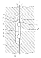
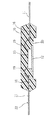
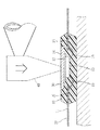
図6に従来のこの種の樹脂パッケージ型半導体装置1の構造例を示す。この半導体装置1は、半導体チップ13と、この半導体チップ13が搭載されるダイパッド12と、半導体チップ13の上面の端子パッドとの間がワイヤボンディングなどによって電気的に導通させられる複数の内部リード16と、この内部リード16と連続して樹脂パッケージ10の側面から外部に延出させられる外部リード11と、上記樹脂パッケージ10の下面に面一状に露出させられる放熱板14とを備えている。この放熱板14は、たとえば銅などの熱伝導性に優れた金属板によって形成される。図6に示される構造の場合、上記放熱板14は、ダイパッド12の下面に対して接合されている。すなわち、この放熱板14は、リードフレームの段階において、ダイパッド12の下面に対して、たとえば超音波接合、あるいはスポット溶接などによってあらかじめ接合される。このようなリードフレームに対して、ダイパッド12に半導体チップ13をボンディングするチップボンディング工程、半導体チップ13と内部リード16とを結線するワイヤボンディング工程を施した後、このリードフレーム22は、樹脂パッケージ工程に供される。樹脂パッケージ工程では、図7に示すように、上下の金型60,61間に上記のリードフレーム22を挟持するようにして、キャビティ空間7内に熱硬化性の樹脂を溶融状態で注入するとともに、これを加熱硬化させる。このように、従来のこの種の樹脂パッケージ型半導体装置においては、上記放熱板14は、樹脂パッケージ工程において、パッケージ内に組み込まれていた。
【0004】
【発明が解決しようとする課題】
ところで、上記リードフレーム22のダイパッド12は、その下面に接合した放熱板14の下面が上記樹脂パッケージ工程においてちょうど下金型のキャビティ71の底面に接するように、あらかじめダウンオフセットさせられている。そして、このダイパッド12は、通常、比較的細い支持リード(図示略)を介して、リードフレーム22に支持されている。そのため、上記ダイパッド12に接合された放熱板14は、非常に不安定であり、外力が作用すれば、容易に姿勢が変化する。その結果、図7に示す樹脂パッケージ工程、より詳しくは、リードフレーム22を挟持するようにして上下の金型60,61の型締めをした状態において、キャビティ空間7内に溶融樹脂を注入する工程において、樹脂の流れの力によって上記の放熱板14の姿勢が狂い、こうして放熱板の姿勢が狂ったまま樹脂が硬化してしまうことがあった。
【0005】
そうすると、たとえば、放熱板14の下面の全部または一部がパッケージの樹脂によって薄バリ状に覆われるといった状態が現出し、しかもその状態が個々の半導体装置によってまちまちとなり、これらは外観的に不良とされ、歩留りの低下が著しかった。
【0006】
また、樹脂パッケージ工程中における上記のような放熱板14の姿勢の変動は、ダイパッド上の半導体チップと内部リードとをつなぐワイヤの接合状態に不良をもたらすこともあり、この場合は、外観的には良品であっても、電気機能的に不良となる。
【0007】
本願発明は、このような事情のもとで考え出されたものであって、外観不良や機能不良の可能性を著しく低減しつつ、放熱板が樹脂パッケージの表面に露出する恰好で備わる樹脂パッケージ型半導体装置の製造方法を提供することをその課題としている。
【0008】
【発明の開示】
上記の課題を解決するため、本願発明では、次の技術的手段を講じている。
【0009】
すなわち、本願発明によって提供される半導体装置の製造方法は、半導体チップと、この半導体チップが搭載されるダイパッドと、上記半導体チップと電気的に導通させられる複数本の内部リードと、上記半導体チップないし上記内部リードを包み込む樹脂パッケージと、上記各内部リードに連続して上記樹脂パッケージの外部に延出する外部リードと、上記樹脂パッケージの表面または裏面に面一状に露出するようにして上記樹脂パッケージ内に埋設された放熱板と、を備える半導体装置の製造方法であって、上記ダイパッド、上記内部リードおよび上記外部リードを含むように形成されたリードフレームを用い、上記ダイパッドの上面に半導体チップをボンディングする工程と、上記半導体チップと上記内部リードとを電気的に導通させる工程と、上記ダイパッド、上記半導体チップないし上記内部リードを樹脂パッケージによって包み込む樹脂パッケージ工程とを含んでおり、上記樹脂パッケージ工程において、樹脂パッケージの表面または裏面に、凹陥部を、その底面に上記ダイパッドの裏面が面一状に露出するようにして形成しておき、上記凹陥部に、この凹陥部の大きさに対してわずかに小さく、かつこの凹陥部の深さと対応した厚みを有する板状の放熱板を、上記ダイパッドの露出面に対して超音波接合することにより嵌め込み固定することに特徴づけられる。
【0010】
すなわち、本願発明方法は、放熱板は、従来のように樹脂パッケージ工程において樹脂パッケージ内に組み込まれるのではなく、樹脂パッケージ工程の後に組み込まれる。すなわち、樹脂パッケージ工程においては、放熱板が嵌まり込むべき凹陥部を設けておき、樹脂パッケージ工程の後、この凹陥部内に嵌め込み固定される。放熱板を嵌め込むのは、リードフレームの状態において行ってもよいし、リードカット工程を経て各半導体装置に分離された後に行ってもよい。
【0011】
したがって、本願発明方法においては、従来のように樹脂パッケージ工程において、キャビティ内に注入される樹脂の流れの力によって放熱板の姿勢が狂い、このように姿勢が狂った状態において樹脂が硬化されてしまうといったことは起こりえない。上記凹陥部を放熱板の形状に対応したものとしておくことにより、この放熱板が適正に樹脂パッケージの表面に露出させられた形態の樹脂パッケージ型半導体装置が得られる。
【0012】
また、同様に、樹脂パッケージ工程において、放熱板の姿勢が変動することによってダイパッド上の半導体チップの姿勢が変動するということもないので、半導体チップと内部リードをつなぐワイヤの接続不良が生じるといったこともなく、機能的な不良の出現もまた、抑制される。
【0013】
【0014】
【0015】
【0016】
【0017】
本願発明のその他の特徴および利点は、図面を参照して以下に行う詳細な説明からち、より明らかとなろう。
【0018】
【発明の実施の形態】
以下、本願発明の好ましい実施形態を、図面を参照しつつ、具体的に説明する。なお、これらの図において、図6および図7に示した従来例と同等の部材または部分には、同一の符号を付してある。
【0019】
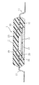
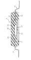
図1は、本願発明の半導体装置の製造方法によって製造された樹脂パッケージ型半導体装置1の一例の断面図である。同図に示されるように、この樹脂パッケージ型半導体装置1は、半導体チップ13が搭載されるダイパッド12と、上記半導体チップ13の上面パッドとの間がワイヤボンディング19によって電気的に導通させられる複数の内部リード16と、これらダイパッド12、半導体チップ13ないし内部リード16を包み込む樹脂パッケージ10と、この樹脂パッケージ10の下面に面一状に露出させられた放熱板14とを備えている。放熱板14は、樹脂パッケージ10の下面に形成した凹陥部20内に嵌め込まれた状態において、上記ダイパッド12の裏面に対して接合されている。両者の接合は、放熱板14およびダイパッド12の双方の中央部において、たとえば超音波接合によって行われる。凹陥部20の深さは、上記放熱板14の厚みと対応させられており、平面的な形状は、放熱板14の平面的な形状と対応させられているが、放熱板14の平面的な大きさよりわずかに大きい。
【0020】
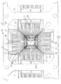
上記構成の樹脂パッケージ型半導体装置1は、たとえば、図2に示すようなリードフレーム22を用いて製造される。これらの図2に示されるリードフレーム22は、いわゆるクワッド・フラット型パッケージを有する半導体装置を製造するためのものである。
【0021】
幅方向両側のサイドフレーム23,23および長手方向等間隔に上記サイドフレーム23,23間を掛け渡すように形成されるクロスフレーム24,24によって囲まれる矩形領域25内に、上記樹脂パッケージ型半導体装置1の構成部分となるべきリード11,16ないしダイパッド12などが打ち抜き形成されている。四辺形枠状のタイバー26がその支持リード27によってサイドフレーム23およびクロスフレーム24に連結されるようにして形成されている。この四辺形枠状のタイバー26の四隅部から内方に延びる吊りリード15によって、矩形状のダイパッド12が支持されている。隣合う吊りリード15,15で区画される各台形領域には、タイバー26に基端が連結され、かつダイパッド12の各辺に向けて延びる複数本の内部リード16が形成されている。タイバー26の外側には、各内部リード16に連続して外方に延びる外部リード11が形成されている。各外部リード11の外端部は、支持リード27を介してサイドフレーム23,23またはクロスフレーム24,24に連結されている。各内部リード16は、概して、ダイパッド12の中心から放射状に延びる方向に形成されている。
【0022】
なお、上記ダイパッド12は、後述するように、樹脂パッケージ工程において、放熱板14の厚みを勘案して深さが設定されて樹脂パッケージ10の裏面に形成される凹陥部20の底面に露出することができるように、リードフレーム22における他の部分に対してダウンオフセットされている。
【0023】
図2に示されているように、上記構成のリードフレーム22のダイパッド12の上面に、半導体チップ13がボンディングされるとともに、この半導体チップ13の上面に形成された電極パッド(図示略)と上記各内部リード16との間がワイヤボンディング19によって結線される。このようにチップボンディング工程およびワイヤボンディング工程を終えたリードフレーム22は、樹脂パッケージ工程に供される。
【0024】
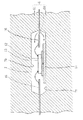
樹脂パッケージ工程装置6は、トランスファモールド法によって上記のリードフレーム22上の所定領域を熱硬化性樹脂によるパッケージで包み込む工程を行う装置であり、図3に示すように、上下方向に相対移動して型締め状態と型開き状態とを選択しうる下金型61および上金型60を備える。下金型61および上金型60には、型締め状態において、上記リードフレーム22上のタイバー26で囲まれた矩形領域に樹脂パッケージ10を形成するに適したキャビティ70,71がそれぞれ形成されている。そして、図3に示す実施形態においては、下金型61のキャビティ71の底部に、放熱板14の形状と対応した膨出部30が形成されている。たとえば、放熱板14が所定厚みの円形をしているのであれば、この膨出部30の平面形態は放熱板14の平面形態と対応した円形とし、膨出部30の膨出高さは、放熱板14の厚みと対応したものとされる。そして、本実施形態においてはとくに、上記膨出部30の上面に、小径の吸引孔80が設けられている。この吸引孔80は、バルブを介して図示しない負圧発生源につながっている。下金型61および/または上金型60における上記キャビティ70,71の隅部には、図示しないランナから送られる溶融樹脂をキャビティ空間内に注入するためのゲート(図示略)が設けられている。
【0025】
上記下金型61と上金型60とを型開きした状態において、下金型61上に上記のようにチップボンディング工程およびワイヤボンディング工程を終えたリードフレーム22を位置決めしつつセットし、図3に示すように両金型60,61を型締めする。この状態において、図3に表れているように、ダイパッド12の裏面は、下金型61のキャビティ71の底面に形成した上記の膨出部30の上面に接触している。本実施形態においては、上記吸引孔80に負圧を作用させて、上記ダイパッド12を確実に上記膨出部30の上面に密着させる。この状態において上記キャビティ空間7内にエポキシ樹脂等の熱硬化性樹脂を溶融状態において注入する。上記ダイパッド12は、吸引力によって上記の膨出部30の上面に密着させられているので、キャビティ空間内に注入される樹脂の流れによってダイパッド12の姿勢が不用意に変動することはない。そして、上記の溶融樹脂は、金型に与えられる熱によって所定時間を経過する間に硬化させられる。
【0026】
上記のような工程を終えた後、上下の金型60,61を型開きすると、図4に示すような断面形状を有する樹脂パッケージ10が形成される。樹脂パッケージ10の裏面側には、上記下金型61のキャビティ70の底面に形成した膨出部30の形態と対応する凹陥部20が形成されており、しかも、この凹陥部20の底面には、ダイパッド12の下面が面一状に臨んでいる。
【0027】
上記樹脂パッケージ10の裏面側に形成された凹陥部20には、たとえば銅などの熱伝導性に優れた金属からなる放熱板14が嵌め込み固定される。本実施形態においては、図5に示すように、上記樹脂パッケージ10を含めたリードフレーム22を反転させて上記樹脂パッケージ10の裏面側を上に向け、そして、上記凹陥部20内に放熱板14を吸着ハンドなどを用いて装填するとともに、超音波ホーン40を用いて上記放熱板14を凹陥部20の底面に向けて圧し付ける。この場合、必要であれば、放熱板14を加熱する。そうすると、超音波振動による相互摩擦により、ダイパッド12と上記放熱板14とは、それらの中央部において、合金化するなどして結合される。
【0028】
以上の工程を終えたリードフレーム22に対して、ハンダメッキ工程、検査工程、標印工程等を行った後、リードカット・フォーミングを施して、図1に示すような個別の樹脂パッケージ型半導体装置1が得られる。
【0029】
本願発明方法によれば、樹脂パッケージ10の表面に露出する放熱板14が、樹脂パッケージ工程の後において、樹脂パッケージ工程において形成された凹陥部20内に嵌め込み固定されるので、この放熱板14の樹脂パッケージ表面における露出形態が一定となる。
【0030】
もちろん、この発明の範囲は上述した実施形態に限定されるものではない。実施形態では、樹脂パッケージの裏面側に凹陥部を設けてこれに放熱板を嵌め込み固定しているが、事情が許せば、樹脂パッケージの表面側に凹陥部を設けてこれに放熱板を嵌め込み固定してもよい。
【0031】
また、実施形態では、凹陥部20の底面にダイパッド12を臨ませ、このダイパッド12に上記放熱板14を連結しているが、凹陥部20の底面にダイパッドを臨ませなくとも、放熱板による大きな放熱効果を期待することができる。この場合、凹陥部への放熱板の固定は、接着等の手段を用いればよい。
【0032】
さらに、実施形態では、リードフレームの状態において、樹脂パッケージ10に設けた凹陥部20に放熱板14を取付けているが、各半導体装置としてリードフレームから分離した後において、必要に応じて樹脂パッケージの表面に設けておいた凹陥部に放熱板を嵌め込み固定する場合も、もちろん、本願発明の範囲に含まれる。
【図面の簡単な説明】
【図1】 本願発明方法によって製造される半導体装置の一例の断面図である。
【図2】 図1に示される半導体装置を製造するためのリードフレームの一例の部分拡大平面図であり、チップボンディングおよびワイヤボンディングを施した状態を示す。
【図3】 図2に示されるリードフレームを用いて本願発明方法によって特徴づけられる樹脂モールド工程を行っている状態を示す模式的断面図である。
【図4】 図3に示される樹脂モールド工程によって得られる中間製品を示す断面図である。
【図5】 図4に示される中間製品に対して放熱板を取付ける工程を示す断面図である。
【図6】 従来例に係る半導体装置の一例を示す断面図である。
【図7】 図6に示される従来例の半導体装置の製造における樹脂モールド工程を示す模式的断面図である。
【符号の説明】
1 半導体装置
10 樹脂パッケージ
11 外部リード
12 ダイパッド
13 半導体チップ
14 放熱板
16 内部リード
20 凹陥部
30 (下金型の)膨出部
6 樹脂パッケージ工程装置
60 上金型
61 下金型
7 キャビティ空間
70 (上金型の)キャビティ
71 (下金型の)キャビティ[0001]
BACKGROUND OF THE INVENTION
The present invention relates to a method for producing a resin packaged semiconductor equipment, and more particularly to a method for producing a resin packaged semiconductor equipment forms the heat radiating plate is provided so as to be exposed on the front surface or the back surface of the resin package.
[0002]
[Prior art]
For example, resin package semiconductor devices that generate a relatively large amount of heat during driving, such as motor drive ICs, certain types of gate arrays, and ultra LSIs, incorporate a heat sink in the resin package, thereby improving heat dissipation performance. Things can be seen.
[0003]
FIG. 6 shows an example of the structure of a conventional resin package type semiconductor device 1 of this type. The semiconductor device 1 includes a plurality of
[0004]
[Problems to be solved by the invention]
By the way, the
[0005]
Then, for example, a state in which all or a part of the lower surface of the
[0006]
Further, the above-described change in the posture of the
[0007]
The present invention has been conceived under such circumstances, and is a resin package provided with a heat sink that is exposed on the surface of the resin package while significantly reducing the possibility of poor appearance and malfunction. An object of the present invention is to provide a method for manufacturing a semiconductor device.
[0008]
DISCLOSURE OF THE INVENTION
In order to solve the above problems, the present invention takes the following technical means.
[0009]
That is, a method of manufacturing a semiconductor device which is herein onset Ming Thus provided, a semiconductor chip, a die pad the semiconductor chip is mounted, and a plurality of inner leads to be allowed to the semiconductor chip and electrically conductive, the semiconductor A resin package that encloses the chip or the internal leads, an external lead that extends to the outside of the resin package continuously to the internal leads, and is exposed to be flush with the front or back surface of the resin package. A semiconductor device manufacturing method comprising: a heat sink embedded in a resin package, wherein a lead frame formed to include the die pad, the internal lead, and the external lead is used, and a semiconductor is formed on an upper surface of the die pad. A step of bonding the chip, and electrically connecting the semiconductor chip and the internal lead. Step and, the die pad includes a resin packaging process encasing said semiconductor chip to the inner leads by a resin package in the resin packaging process, the surface or the back surface of the resin package, the die pad a recess in its bottom surface the advance back surface forms shape so as to be exposed in flush with a plate having the above recess, a rather slight small for the size, and the corresponding depth of the concave portion the thickness of the recess It is characterized in that the heat sink is fitted and fixed by ultrasonic bonding to the exposed surface of the die pad.
[0010]
That is, according to the method of the present invention, the heat radiating plate is not incorporated in the resin package in the resin package process as in the prior art, but is incorporated after the resin package process. That is, in the resin packaging process, a recessed part into which the heat sink is to be fitted is provided, and after the resin packaging process, it is fitted and fixed in the recessed part. The heat sink may be inserted in the state of the lead frame, or may be performed after being separated into each semiconductor device through a lead cutting process.
[0011]
Therefore, in the method of the present invention, in the conventional resin packaging process, the heat sink is misaligned by the force of the resin flow injected into the cavity, and the resin is cured in such a misaligned state. It can never happen. By setting the concave portion to correspond to the shape of the heat sink, a resin package type semiconductor device in which the heat sink is appropriately exposed on the surface of the resin package can be obtained.
[0012]
Similarly, in the resin packaging process, since the attitude of the semiconductor chip on the die pad does not change due to the change in the attitude of the heat sink, the connection failure of the wire connecting the semiconductor chip and the internal lead occurs. And the appearance of functional defects is also suppressed.
[0013]
[0014]
[0015]
[0016]
[0017]
Other features and advantages of the present invention will become more apparent from the detailed description given below with reference to the drawings.
[0018]
DETAILED DESCRIPTION OF THE INVENTION
Hereinafter, preferred embodiments of the present invention will be specifically described with reference to the drawings. In these drawings, members or portions equivalent to those of the conventional example shown in FIGS. 6 and 7 are denoted by the same reference numerals.
[0019]
FIG. 1 is a cross-sectional view of an example of a resin package type semiconductor device 1 manufactured by the method for manufacturing a semiconductor device of the present invention. As shown in the figure, the resin package type semiconductor device 1 includes a plurality of electrical connection between a
[0020]
The resin package type semiconductor device 1 having the above configuration is manufactured using, for example, a
[0021]
The resin package type semiconductor device is formed in a rectangular region 25 surrounded by side frames 23, 23 on both sides in the width direction and cross
[0022]
As will be described later, the
[0023]
As shown in FIG. 2, the
[0024]
The resin
[0025]
In a state where the
[0026]
After the above steps are completed, when the upper and
[0027]
The
[0028]
The
[0029]
According to the method of the present invention, the
[0030]
Of course, the scope of the present invention is not limited to the embodiment described above. In the embodiment, a concave portion is provided on the back side of the resin package and a heat sink is fitted and fixed thereto. However, if circumstances permit, a concave portion is provided on the surface side of the resin package and a heat sink is fitted and fixed thereto. May be.
[0031]
In the embodiment, the
[0032]
Furthermore, in the embodiment, the
[Brief description of the drawings]
FIG. 1 is a cross-sectional view of an example of a semiconductor device manufactured by a method of the present invention.
2 is a partially enlarged plan view of an example of a lead frame for manufacturing the semiconductor device shown in FIG. 1, showing a state in which chip bonding and wire bonding are performed.
FIG. 3 is a schematic cross-sectional view showing a state in which a resin molding process characterized by the method of the present invention is performed using the lead frame shown in FIG. 2;
4 is a cross-sectional view showing an intermediate product obtained by the resin molding step shown in FIG.
5 is a cross-sectional view showing a process of attaching a heat sink to the intermediate product shown in FIG.
FIG. 6 is a cross-sectional view showing an example of a semiconductor device according to a conventional example.
7 is a schematic cross-sectional view showing a resin molding step in manufacturing the conventional semiconductor device shown in FIG. 6;
[Explanation of symbols]
DESCRIPTION OF SYMBOLS 1
Claims (1)
上記ダイパッド、上記内部リードおよび上記外部リードを含むように形成されたリードフレームを用い、
上記ダイパッドの上面に半導体チップをボンディングする工程と、
上記半導体チップと上記内部リードとを電気的に導通させる工程と、
上記ダイパッド、上記半導体チップないし上記内部リードを樹脂パッケージによって包み込む樹脂パッケージ工程とを含んでおり、
上記樹脂パッケージ工程において、樹脂パッケージの表面または裏面に、凹陥部を、その底面に上記ダイパッドの裏面が面一状に露出するようにして形成しておき、
上記凹陥部に、この凹陥部の大きさに対してわずかに小さく、かつこの凹陥部の深さと対応した厚みを有する板状の放熱板を、上記ダイパッドの露出面に対して超音波接合することにより嵌め込み固定することを特徴とする、半導体装置の製造方法。A semiconductor chip; a die pad on which the semiconductor chip is mounted; a plurality of internal leads that are electrically connected to the semiconductor chip; a resin package that encloses the semiconductor chip or the internal leads; and continuous to the internal leads. A semiconductor device comprising: an external lead extending to the outside of the resin package; and a heat sink embedded in the resin package so as to be exposed on the front or back surface of the resin package. A method,
Using a lead frame formed to include the die pad, the internal lead and the external lead,
Bonding a semiconductor chip to the upper surface of the die pad;
Electrically connecting the semiconductor chip and the internal lead;
A resin package step of wrapping the die pad, the semiconductor chip or the internal lead with a resin package,
In the resin packaging process, the surface or the back surface of the resin package, the concave portion, the back surface of the die pad advance form shape so as to be exposed in flush with the bottom surface thereof,
In the recess slightly rather small for the size of the recess, and a plate-shaped radiator plate having a depth and the corresponding thickness of the recess, ultrasonically bonded to the exposed surface of the die pad A method of manufacturing a semiconductor device, wherein the method is fitted and fixed.
Priority Applications (1)
| Application Number | Priority Date | Filing Date | Title |
|---|---|---|---|
| JP01156297A JP3813680B2 (en) | 1997-01-24 | 1997-01-24 | Manufacturing method of semiconductor device |
Applications Claiming Priority (1)
| Application Number | Priority Date | Filing Date | Title |
|---|---|---|---|
| JP01156297A JP3813680B2 (en) | 1997-01-24 | 1997-01-24 | Manufacturing method of semiconductor device |
Publications (2)
| Publication Number | Publication Date |
|---|---|
| JPH10209341A JPH10209341A (en) | 1998-08-07 |
| JP3813680B2 true JP3813680B2 (en) | 2006-08-23 |
Family
ID=11781385
Family Applications (1)
| Application Number | Title | Priority Date | Filing Date |
|---|---|---|---|
| JP01156297A Expired - Fee Related JP3813680B2 (en) | 1997-01-24 | 1997-01-24 | Manufacturing method of semiconductor device |
Country Status (1)
| Country | Link |
|---|---|
| JP (1) | JP3813680B2 (en) |
Families Citing this family (2)
| Publication number | Priority date | Publication date | Assignee | Title |
|---|---|---|---|---|
| KR20020021476A (en) * | 2000-09-15 | 2002-03-21 | 이중구 | Chip scale semiconductor package and manufacturing method therefor |
| JP6076675B2 (en) | 2011-10-31 | 2017-02-08 | ローム株式会社 | Semiconductor device |
-
1997
- 1997-01-24 JP JP01156297A patent/JP3813680B2/en not_active Expired - Fee Related
Also Published As
| Publication number | Publication date |
|---|---|
| JPH10209341A (en) | 1998-08-07 |
Similar Documents
| Publication | Publication Date | Title |
|---|---|---|
| US5091341A (en) | Method of sealing semiconductor device with resin by pressing a lead frame to a heat sink using an upper mold pressure member | |
| JP3205235B2 (en) | Lead frame, resin-encapsulated semiconductor device, method of manufacturing the same, and mold for manufacturing semiconductor device used in the manufacturing method | |
| JP2927660B2 (en) | Method for manufacturing resin-encapsulated semiconductor device | |
| EP0484297B1 (en) | Process for assembling and resin-encapsulating a semiconductor power device mounted on a heat sink | |
| US6893898B2 (en) | Semiconductor device and a method of manufacturing the same | |
| CN110828432B (en) | Power semiconductor module | |
| US5445995A (en) | Method for manufacturing plastic-encapsulated semiconductor devices with exposed metal heat sink | |
| JP3813680B2 (en) | Manufacturing method of semiconductor device | |
| US12334408B2 (en) | Semiconductor device and method for manufacturing semiconductor device | |
| CN222720429U (en) | Hybrid quad flat no-lead QFN and quad flat package QFP integrated circuit package | |
| JP2010118577A (en) | Resin encapsulated semiconductor device and method of manufacturing the same | |
| JP3616469B2 (en) | Semiconductor device and manufacturing method thereof | |
| CN101326636A (en) | Apparatus and method for assembling packaged semiconductor with top and bottom exposed | |
| JP2012174747A (en) | Power semiconductor module structure and manufacturing method of the same | |
| JP3688760B2 (en) | Resin package type semiconductor device and manufacturing method thereof | |
| JP5119092B2 (en) | Manufacturing method of semiconductor device | |
| JPH10209194A5 (en) | ||
| JP3660444B2 (en) | Resin package type semiconductor device and manufacturing method thereof | |
| JP3442911B2 (en) | Resin package type semiconductor device and method of manufacturing the same | |
| JP3402194B2 (en) | Lead frame | |
| JP4201060B2 (en) | Semiconductor device and manufacturing method thereof | |
| JP3732604B2 (en) | Resin package type semiconductor device and manufacturing method thereof | |
| JPH08274234A (en) | Semiconductor device, method of manufacturing the same, and semiconductor mounting module | |
| JP2001196401A (en) | Method for forming resin package of semiconductor device | |
| JP2000031367A (en) | Semiconductor device and manufacturing method thereof |
Legal Events
| Date | Code | Title | Description |
|---|---|---|---|
| A977 | Report on retrieval |
Free format text: JAPANESE INTERMEDIATE CODE: A971007 Effective date: 20041005 |
|
| A131 | Notification of reasons for refusal |
Free format text: JAPANESE INTERMEDIATE CODE: A131 Effective date: 20050712 |
|
| A521 | Request for written amendment filed |
Free format text: JAPANESE INTERMEDIATE CODE: A523 Effective date: 20050909 |
|
| A02 | Decision of refusal |
Free format text: JAPANESE INTERMEDIATE CODE: A02 Effective date: 20051206 |
|
| A521 | Request for written amendment filed |
Free format text: JAPANESE INTERMEDIATE CODE: A523 Effective date: 20060203 |
|
| A911 | Transfer to examiner for re-examination before appeal (zenchi) |
Free format text: JAPANESE INTERMEDIATE CODE: A911 Effective date: 20060222 |
|
| TRDD | Decision of grant or rejection written | ||
| A01 | Written decision to grant a patent or to grant a registration (utility model) |
Free format text: JAPANESE INTERMEDIATE CODE: A01 Effective date: 20060530 |
|
| A61 | First payment of annual fees (during grant procedure) |
Free format text: JAPANESE INTERMEDIATE CODE: A61 Effective date: 20060601 |
|
| R150 | Certificate of patent or registration of utility model |
Free format text: JAPANESE INTERMEDIATE CODE: R150 |
|
| FPAY | Renewal fee payment (event date is renewal date of database) |
Free format text: PAYMENT UNTIL: 20100609 Year of fee payment: 4 |
|
| FPAY | Renewal fee payment (event date is renewal date of database) |
Free format text: PAYMENT UNTIL: 20110609 Year of fee payment: 5 |
|
| FPAY | Renewal fee payment (event date is renewal date of database) |
Free format text: PAYMENT UNTIL: 20120609 Year of fee payment: 6 |
|
| FPAY | Renewal fee payment (event date is renewal date of database) |
Free format text: PAYMENT UNTIL: 20130609 Year of fee payment: 7 |
|
| LAPS | Cancellation because of no payment of annual fees |