JP3813636B2 - Fast input buffer - Google Patents
Fast input buffer Download PDFInfo
- Publication number
- JP3813636B2 JP3813636B2 JP52071598A JP52071598A JP3813636B2 JP 3813636 B2 JP3813636 B2 JP 3813636B2 JP 52071598 A JP52071598 A JP 52071598A JP 52071598 A JP52071598 A JP 52071598A JP 3813636 B2 JP3813636 B2 JP 3813636B2
- Authority
- JP
- Japan
- Prior art keywords
- circuit
- input
- signal
- sense amplifier
- response
- Prior art date
- Legal status (The legal status is an assumption and is not a legal conclusion. Google has not performed a legal analysis and makes no representation as to the accuracy of the status listed.)
- Expired - Fee Related
Links
Images


Classifications
-
- G—PHYSICS
- G11—INFORMATION STORAGE
- G11C—STATIC STORES
- G11C7/00—Arrangements for writing information into, or reading information out from, a digital store
- G11C7/10—Input/output [I/O] data interface arrangements, e.g. I/O data control circuits, I/O data buffers
- G11C7/1078—Data input circuits, e.g. write amplifiers, data input buffers, data input registers, data input level conversion circuits
- G11C7/1093—Input synchronization
-
- G—PHYSICS
- G11—INFORMATION STORAGE
- G11C—STATIC STORES
- G11C7/00—Arrangements for writing information into, or reading information out from, a digital store
-
- G—PHYSICS
- G11—INFORMATION STORAGE
- G11C—STATIC STORES
- G11C7/00—Arrangements for writing information into, or reading information out from, a digital store
- G11C7/10—Input/output [I/O] data interface arrangements, e.g. I/O data control circuits, I/O data buffers
- G11C7/1015—Read-write modes for single port memories, i.e. having either a random port or a serial port
- G11C7/1042—Read-write modes for single port memories, i.e. having either a random port or a serial port using interleaving techniques, i.e. read-write of one part of the memory while preparing another part
-
- G—PHYSICS
- G11—INFORMATION STORAGE
- G11C—STATIC STORES
- G11C7/00—Arrangements for writing information into, or reading information out from, a digital store
- G11C7/10—Input/output [I/O] data interface arrangements, e.g. I/O data control circuits, I/O data buffers
- G11C7/1078—Data input circuits, e.g. write amplifiers, data input buffers, data input registers, data input level conversion circuits
-
- G—PHYSICS
- G11—INFORMATION STORAGE
- G11C—STATIC STORES
- G11C7/00—Arrangements for writing information into, or reading information out from, a digital store
- G11C7/22—Read-write [R-W] timing or clocking circuits; Read-write [R-W] control signal generators or management
Landscapes
- Dram (AREA)
- Static Random-Access Memory (AREA)
Description
発明の技術分野
本発明は、一般に集積回路に関し、そして詳細には、本発明は、高速なデータ伝送を受け取り得るデータ入力バッファに関する。
発明の背景
集積回路は通常、付加的な回路と通信するために使用される多くの入力/出力ピンを含む。例えば、ダイナミックランダムアクセスメモリ(DRAM)などの集積メモリ装置は、メモリ動作制御信号を受け取るための制御入力、および外部のシステムまたはプロセッサとの相方向データ通信のためのデータピンの両方を含む。
現在の集積回路のデータ伝送速度は、主に内部回路動作速度によって制限される。すなわち、多くの集積回路の容量より速い速度で回路間において信号を伝送し得る通信ネットワークが開発されてきた。より速い回路への要求に対応するために、1グループの集積回路が共通バス上に組合せされ得る。この構成において、各集積回路は、他の集積回路と協調されたやり方で動作し、高速度で伝送されるデータを共有する。例えば、1グループの、DRAM、スタティックRAM、または読み取り専用メモリ(ROM)などのメモリ装置が共通のデータバスに接続され得る。バスのデータ速度は、個々のメモリの可能な動作速度より実質的に速くあり得る。したがって、各メモリは、1つのメモリが入力されたデータを処理しながら、別メモリが新しいデータを受け取るように動作される。適切な数のメモリ装置および効率的な制御システムを提供することによって、非常に高速なデータ伝送が達成され得る。
データ通信信号の伝送速度が増加し続けるにつれて、新しい回路および方法が、各集積回路で正確にデータを受け取るために必要とされる。1つの提案された解法は、米国特許第5,513,327号に記載されるバスインターフェースである。このバスインターフェースは、データをラッチするために2つのエッジトリガ受信器を使用する。第1の受信器は、クロック信号の立ち上がりエッジに応答して動作し、他方第2の受信器は、クロックの立ち下がりエッジに応答して動作する。さらに、データバスは、中間供給レベルで終端されず、そして出力は、オープンドレイン(open drain)構成を使用してバス上を伝送される。
上述の理由、および本明細書を読みおよび理解する際に当業者にとって明らかである、以下に述べられる他の理由のために、バスクロックの推移に応答してデータを受け取るために、独立にまたは他の入力バッファと組み合わせて、動作し得る高速入力バッファに対する当該技術分野における要求がある。
発明の要旨
集積回路データ伝送についての上記の問題および他の問題が、本発明によって対応され、そして以下の明細書を読みおよび検討することによって理解される。各クロック信号上のデータ信号を平衡化、サンプリング、感知、およびラッチする入力バッファ回路が説明される。
詳細には、本発明は、高速データバスに結合されるように適合された入力バッファ回路を説明する。入力バッファ回路は、データ入力ノードおよびデータバス終端電圧に選択的に結合される差動感知増幅器回路を備える。平衡回路は、差動感知増幅器回路、および平衡信号に応答して差動感知増幅器回路をデータバス終端電圧へ平衡化するためのデータバス終端電圧に接続される。結合回路は、サンプル信号に応答してデータ入力ノードおよびデータバス終端電圧を差動感知増幅器回路に選択的に結合させるために提供される。入力バッファはさらに、感知信号に応答して差動感知増幅器回路を作動させるための感知増幅器作動回路を含む。ラッチ回路は、差動感知増幅器回路に結合される。ラッチ回路は、ラッチ信号に応答して差動感知増幅器回路のデータ状態をラッチするために適合される。
【図面の簡単な説明】
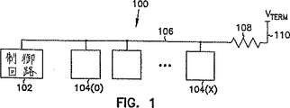
図1は、メモリバスの図である。
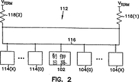
図2は、別のメモリバスの図である。
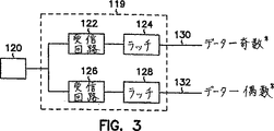
図3は、デュアル受信入力バッファ回路のブロック図である。
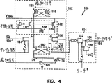
図4は、単一受信高速入力バッファの模式図である。
図5は、図4の入力バッファの動作のタイミング図である。
図6は、図4の入力バッファの選択電圧のタイミング図である。
図7は、別の高速入力バッファの模式図である。
図8A、B、およびCは、図7の入力バッファの動作のタイミング図である。
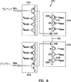
図9は、出力ドライバ回路の模式図である。
図10は、高速入力バッファを内蔵するメモリ装置のブロック図である。
発明の詳細な説明
好ましい実施態様の以下の詳細な説明において、本明細書の一部分をなし、そして発明が実施され得る具体的な好ましい実施態様を例示するやり方によって示される付属の図面が参照される。これらの実施態様は、当業者が発明を実施することを可能にするために十分詳細に説明され、そして他の実施態様が利用され得ること、ならびに論理的、機械的、および電気的変更が本発明の精神および範囲を逸脱せずになされ得ることが理解される。したがって、以下の詳細な説明は、限定する意味に受け取られるものではなく、そして本発明の範囲は、付属の請求項によってのみ定義される。
図1は、複数の通信線106を介して多くの集積回路104(0)〜104(x)へ制御およびデータ信号を提供するために制御回路102を含むメモリバス100の簡略化された例示である。通信線は、終端電圧(Vterm)に結合された適切な終端回路108(一般に、レジスタとして例示される)を用いて終端される。
図2は、複数の通信線116を介して多くの集積回路104(0)〜104(x)および114(0)〜114(x)へ制御およびデータ信号を提供するために中心に位置付けられた制御回路102を含むメモリバス112の簡略化された例示である。通信線は、終端電圧(Vterm)に結合される適切な終端回路118(1)および118(2)(一般に、レジスタとして例示される)を用いて両端で終端される。Vtermの好ましい値は、1/2(Vdd−Vss)であるが、任意の中間供給レベルであり得る。
図3は、データ入力120に接続された入力バッファ119のブロック図である。バッファは、平行に接続された2つの受信回路122および126ならびに2つのラッチ回路124および128を含む。各ラッチ回路は、ノード130(データ奇数*)またはノード132(データ偶数*)のいずれかの上のデータ出力を生成する。受信器は、バス線上に提供される共通のデータクロック信号の異なる位相から外れて動作する。したがって、受信器は、エッジトリガされず、内部バーニア(vernier)遅延を使用して制御される。バーニア遅延は、有効なデータ受信を最大化するためにシステム作動時に調整される。すなわち、遅延は、データサンプリングが有効なデータが存在する場合に行われ、そしてクロック信号のエッジ遷移に制限されないように調整される。例示されるデュアル受信入力バッファは、1秒当たり800+メガビットの範囲で高速データ通信に使用され得る。1秒当たり400メガビットといった、より遅いデータ通信速度については、単一受信器およびラッチ回路が入力バッファにおいて使用され得る。
図4を参照すると、受信器152およびラッチ回路154を用いて出力156上に内部データ信号(Data)を生成する高速入力バッファ150が説明される。受信器152回路は、他の集積回路に結合されたバス上に提供された、異なる位相の共通のクロック信号に基づく内部信号に応答して動作する。内部信号は、平衡信号(equilibrate signal)(EQ*)、感知信号(Sense)、およびサンプル信号(Sample)である。受信器は、バス終端電圧(Vterm)に接続され、且つデータ入力コネクション120を介してバスデータラインに接続される。
受信器152は、1対の交差結合されたp型トランジスタを有するp型感知増幅器回路158および1対の交差結合されたn型トランジスタを有するn型感知増幅器160からなる。感知増幅器の共通のノード(ノードAおよびB)をVtermに平衡化するために、平衡回路162が提供される。結合回路164および166が提供され、サンプル信号に応答してノード120およびVtermをそれぞれノードAおよびBに選択的に結合する。入力バッファの動作をよりよく理解するために、図5のタイミング図を参照する。
図5に示すように、平衡信号(EQ*)は時間t1においてローに遷移し、平衡回路162のトランジスタ168、170および172を作動させる。トランジスタ170および172はそれぞれノードBおよびAを終端電圧Vtermに結合する。従って感知増幅器はバス終端電圧に平衡化される。時間t2において、平衡回路は停止され、サンプル信号はハイに遷移し、結合回路164を作動させて、入力120をノードAに結合する。同様に結合回路166が作動させられ、ノードBを終端電圧Vtermに結合する。時間t2においてローの感知信号で、p型感知増幅器回路158のノード180はローに結合され、n型感知増幅器のノード174はトランジスタ176を介してVtermに結合される。時間t3において、感知信号はハイに遷移し、トランジスタ178を作動させ、ノード174をグラウンドに結合する。サンプル信号はローに遷移し、p型感知増幅器およびn型感知増幅器がノードAおよびBを適切な電圧レベルに増幅するようにノードAおよびBを分離する。ラッチ*信号は時間t3においてハイに遷移し、ラッチ回路154を作動させる。従って、結合回路182が作動させられ、ノードBの逆をインバータ回路184に結合する。ラッチ*信号がローの状態に戻ると、回路182が停止させられ、且つ回路186が作動させられインバータ184をラッチする。ラッチはノードBに接続されるが、ラッチ回路154はノードAに結合され得、本発明を制限する意図はない。外部から受け取られたクロック信号に応答して、図5に示した信号が内部で生成されることが、当業者によって理解される。このように、入力データバッファは異なる位相のクロック信号に依存して動作する。
図6は、ハイの入力データ信号を受け取った時の、ノードAおよびB上の電圧および出力ノード156を示す。時間t1において、ノードAおよびBはVtermに平衡化される。時間t2において、ノードAは入力120に結合され電圧を上昇させる。時間t3において、感知増幅器回路が作動させられ、ノードAおよびBを増幅する。同時に、ノードBはラッチ回路に結合され、156上の出力データ信号はノードBに結合される。
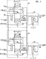
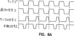
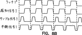
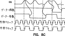
図7は、図3に示した2つの並列受信器122および126、ならびに2つのラッチ回路124および128を有する高速入力バッファの概略図を示す。図4を参照しながら上記で説明したように、受信器122および126は通常、受信器152の回路を含み、同様の様態で動作する。図8A、8Bおよび8Cのタイミング図は図7の高速入力バッファの動作を示す。DQライン上に提供されたデータ信号は、それぞれのサンプル信号の上昇するエッジ上において受信器122および126の両方によってサンプルされる。従って、DQラインは両受信器回路によってサンプルされる。出力(データ−偶数*およびデータ−奇数*)が共に、DQライン上に提供されたデータを示す。外部バスクロック信号および外部クロックの2倍の周波数で動作する内部クロック信号を説明する。平衡信号(EQ1*およびEQ2*)は実質的にクロック信号と整列している。外部クロック信号は理論上、1/2(EQ1*AND EQ2*)に等しいものと定義され得る。サンプル信号は、データ信号が信号ピークにある場合に、DQラインをサンプルするように、バーニア遅延回路を用いて調整される。
図9は、集積回路のデータ出力コネクション(DQ)に接続されたプッシュ/プル出力ドライバ200の概略図である。プルアップ信号およびプルダウン信号はそれぞれノード202および204に提供され、プルアップトランジスタ206またはプルダウントランジスタ208のいずれかを作動させる。ドライバ回路は任意のスルー・レート制御回路210を備える。制御回路はVslew信号を用いて調整され、選択的に一連のトランジスタを作動させ得る。つまり、いずれかのトランジスタを作動させることにより、並列抵抗器がバイパスされ、回路の応答時間が変化する。このようにして、トランジスタ206および208の作動のタイミングが調整され得る。
プルアップ駆動調整回路214が出力ドライバ回路200内に提供され、プルアップトランジスタ206に結合された電圧を調整する。同様に、プルダウン駆動調整回路216が出力ドライバ回路200内に提供され、プルダウントランジスタ206に結合された電圧を調整する。動作において、トランジスタ218のゲートが選択的に作動され、抵抗器220をバイパスする。集積回路がバス上に設置された後に、出力ドライバ回路の調整が行われる。つまり、出力ドライバ電圧は特定のバスシステムの要求に適合するように調整される。スルー・レート制御回路が、本発明から逸れることなく除去され得ることが当業者によって理解される。
図10は、上記の高速入力バッファ248を組み込むダイナミックランダムアクセスメモリ装置240(DRAM)のブロック図である。メモリは、入力ライン243上に提供されたアドレス信号に応答してメモリアレイ241にアクセスするためのアドレス回路242を含む。制御回路252が提供され、制御信号254に応答してメモリの読み出し動作および書き込み動作を制御する。位相発生器回路244が提供され、入力バッファ回路について、内部信号DQ*、サンプル信号、感知信号、およびラッチ*信号を発生させる。バーニア調整回路245が、内部信号のタイミングを調整するための位相発生器に結合される。入力バッファ回路248は、各データラインDQについて、上記の高速入力バッファ回路を含むことが理解される。出力ドライバ回路250が提供され、DQライン上の適切な出力信号を駆動する。図10の具体例はDRAMであるが、本発明の高速入力バッファ回路はSRAMおよびROMメモリ装置等の任意の集積回路装置に含まれ得る。
結論
受信器回路およびサンプルへのラッチを用い且つデータ信号をラッチする集積回路入力バッファ回路が説明される。バッファは、異なる位相の外部から提供されたクロック信号で発生した内部信号に応答して動作する。入力バッファは、より高い伝送速度で動作するデータバス上で使用される2つの受信器回路および2つのラッチ回路を含み得る。受信器回路は、入力データ信号を感知するための感知回路、感知回路を平衡化するための平衡回路、および感知回路を作動させるための感知活性回路を含む。
本明細書中、特定の実施形態を図示且つ説明したが、同じ目的を達成すると推定される任意の構成を本明細書中に示した特定の実施形態と置換し得ることが当業者によって理解され得る。この適用は、本発明のあらゆる適合または改変をカバーするものである。従って、本発明が本発明の請求の範囲およびその相当物によってのみ制限されることは明らかである。 TECHNICAL FIELD OF THE INVENTION The present invention relates generally to integrated circuits, and in particular, the present invention relates to a data input buffer that can receive high speed data transmission.
BACKGROUND OF THE INVENTION Integrated circuits typically include a number of input / output pins that are used to communicate with additional circuitry. For example, an integrated memory device, such as a dynamic random access memory (DRAM), includes both a control input for receiving memory operation control signals and a data pin for phased data communication with an external system or processor.
The data transmission speed of current integrated circuits is limited mainly by the internal circuit operating speed. That is, communication networks have been developed that can transmit signals between circuits at a rate faster than the capacity of many integrated circuits. To accommodate the demand for faster circuits, a group of integrated circuits can be combined on a common bus. In this configuration, each integrated circuit operates in a coordinated manner with other integrated circuits and shares data transmitted at high speed. For example, a group of memory devices such as DRAM, static RAM, or read only memory (ROM) may be connected to a common data bus. The data rate of the bus can be substantially faster than the possible operating speed of the individual memory. Thus, each memory is operated such that one memory processes incoming data while another memory receives new data. By providing an appropriate number of memory devices and an efficient control system, very high speed data transmission can be achieved.
As the transmission rate of data communication signals continues to increase, new circuits and methods are required to accurately receive data at each integrated circuit. One proposed solution is the bus interface described in US Pat. No. 5,513,327. This bus interface uses two edge triggered receivers to latch data. The first receiver operates in response to the rising edge of the clock signal, while the second receiver operates in response to the falling edge of the clock signal. In addition, the data bus is not terminated at an intermediate supply level, and the output is transmitted over the bus using an open drain configuration.
In order to receive data in response to a bus clock transition, either independently or for the reasons described above and other reasons described below, which will be apparent to those skilled in the art upon reading and understanding this specification There is a need in the art for a high speed input buffer that can operate in combination with other input buffers.
SUMMARY OF THE INVENTION The above and other problems with integrated circuit data transmission are addressed by the present invention and will be understood by reading and studying the following specification. An input buffer circuit is described that balances, samples, senses, and latches the data signal on each clock signal.
In particular, the present invention describes an input buffer circuit adapted to be coupled to a high speed data bus. The input buffer circuit comprises a differential sense amplifier circuit that is selectively coupled to a data input node and a data bus termination voltage. The balanced circuit is connected to a differential sense amplifier circuit and a data bus termination voltage for balancing the differential sense amplifier circuit to the data bus termination voltage in response to a balanced signal. A coupling circuit is provided for selectively coupling the data input node and the data bus termination voltage to the differential sense amplifier circuit in response to the sample signal. The input buffer further includes a sense amplifier activation circuit for activating the differential sense amplifier circuit in response to the sense signal. The latch circuit is coupled to the differential sense amplifier circuit. The latch circuit is adapted to latch the data state of the differential sense amplifier circuit in response to the latch signal.
[Brief description of the drawings]
FIG. 1 is a diagram of a memory bus.
FIG. 2 is a diagram of another memory bus.
FIG. 3 is a block diagram of the dual reception input buffer circuit.
FIG. 4 is a schematic diagram of a single reception high-speed input buffer.
FIG. 5 is a timing diagram of the operation of the input buffer of FIG.
FIG. 6 is a timing diagram of the selection voltage of the input buffer of FIG.
FIG. 7 is a schematic diagram of another high-speed input buffer.
8A, B, and C are timing diagrams of the operation of the input buffer of FIG.
FIG. 9 is a schematic diagram of an output driver circuit.
FIG. 10 is a block diagram of a memory device incorporating a high-speed input buffer.
DETAILED DESCRIPTION OF THE INVENTION In the following detailed description of the preferred embodiments, the accompanying drawings that form a part hereof and are shown by way of illustration of specific preferred embodiments in which the invention may be practiced. Is referenced. These embodiments are described in sufficient detail to enable those skilled in the art to practice the invention, and other embodiments can be utilized, as well as logical, mechanical, and electrical changes are described herein. It will be understood that this may be done without departing from the spirit and scope of the invention. The following detailed description is, therefore, not to be taken in a limiting sense, and the scope of the present invention is defined only by the appended claims.
FIG. 1 is a simplified illustration of a
FIG. 2 is centrally located to provide control and data signals to a number of integrated circuits 104 (0) -104 (x) and 114 (0) -114 (x) via
FIG. 3 is a block diagram of the
Referring to FIG. 4, a high
As shown in FIG. 5, the balanced signal (EQ * ) transitions low at time t1, activating
FIG. 6 shows the voltage on nodes A and B and the
FIG. 7 shows a schematic diagram of a high-speed input buffer having two
FIG. 9 is a schematic diagram of a push /
A pull-up
FIG. 10 is a block diagram of a dynamic random access memory device 240 (DRAM) incorporating the high
CONCLUSION An integrated circuit input buffer circuit is described that uses a receiver circuit and a latch to sample and latches the data signal. The buffer operates in response to an internal signal generated by an externally provided clock signal having a different phase. The input buffer may include two receiver circuits and two latch circuits used on the data bus operating at a higher transmission rate. The receiver circuit includes a sensing circuit for sensing an input data signal, a balancing circuit for balancing the sensing circuit, and a sensing activation circuit for operating the sensing circuit.
While specific embodiments have been illustrated and described herein, it will be understood by those of skill in the art that any configuration that is presumed to accomplish the same purpose may be substituted for the specific embodiments illustrated herein. obtain. This application covers any adaptations or modifications of the present invention. Thus, it is manifest that the invention is limited only by the claims and the equivalents thereof.
Claims (19)
データ入力ノードおよびデータバス終端電圧に選択的に結合された差動感知増幅器回路であって、第1および第2の入力/出力ノードと、該第1の入力/出力ノードに結合されたドレインおよび該第2の入力/出力ノードに結合されたゲートを有する第1のp型トランジスタと、該第1の入力/出力ノードに結合されたドレインおよび該第2の入力/出力ノードに結合されたゲートを有する第1のn型トランジスタと、該第2の入力/出力ノードに結合されたドレインおよび該第1の入力/出力ノードに結合されたゲートを有する第2のp型トランジスタと、該第2の入力/出力ノードに結合されたドレインおよび該第1の入力/出力ノードに結合されたゲートを有する第2のn型トランジスタとを含む差動感知増幅器回路と、
該差動感知増幅器回路および該データバス終端電圧に接続され、平衡信号に応答して該差動感知増幅器回路を該データバス終端電圧に平衡化する平衡回路であって、該平衡信号に応答して、該データバス終端電圧を該第1および第2の入力/出力ノードに結合する少なくとも1つのトランジスタと、該平衡信号に応答して、該第1および第2の入力/出力ノードを互いに結合する平衡トランジスタとを含む平衡回路と、
サンプル信号に応答して、該データ入力ノードを該差動感知増幅器回路の該第1の入力/出力ノードに選択的に結合し、該データバス終端電圧を該差動感知増幅器回路の該第2の入力/出力ノードに選択的に結合する結合回路と、
感知信号に応答して該差動感知増幅器回路を作動させる感知増幅器作動回路であって、該感知信号に応答して、該第1および第2のp型トランジスタのそれぞれのソースに第1の供給電圧を結合する第1のトランジスタと、該感知信号に応答して、該第1および第2のn型トランジスタのそれぞれのソースに第2の供給電圧を結合する第2のトランジスタとを含む感知増幅器作動回路と、
該差動感知増幅器回路に結合され、ラッチ信号に応答して該差動感知増幅器回路のデータ状態をラッチするように適合されたラッチ回路と
を含む入力バッファ回路。An input buffer circuit adapted to be coupled to a high speed data bus,
A differential sense amplifier circuit selectively coupled to a data input node and a data bus termination voltage , the first and second input / output nodes, a drain coupled to the first input / output node, and A first p-type transistor having a gate coupled to the second input / output node; a drain coupled to the first input / output node; and a gate coupled to the second input / output node A second n-type transistor having a drain coupled to the second input / output node and a gate coupled to the first input / output node; and A differential sense amplifier circuit including a second n-type transistor having a drain coupled to a first input / output node and a gate coupled to the first input / output node ;
A balanced circuit connected to the differential sense amplifier circuit and the data bus termination voltage and responsive to the balanced signal for balancing the differential sense amplifier circuit to the data bus termination voltage , the responsive to the balanced signal At least one transistor for coupling the data bus termination voltage to the first and second input / output nodes and the first and second input / output nodes to each other in response to the balanced signal A balanced circuit including a balanced transistor to
In response to the sample signal, said data input node selectively coupled to the first input / output nodes of the differential sense amplifier circuit, the data bus termination voltage differential sense amplifier circuit of the second the A coupling circuit that selectively couples to the input / output nodes of
A sense amplifier actuation circuit that activates the differential sense amplifier circuit in response to a sense signal , wherein a first supply is provided to each source of the first and second p-type transistors in response to the sense signal . A sense amplifier that includes a first transistor that couples a voltage and a second transistor that couples a second supply voltage to respective sources of the first and second n-type transistors in response to the sense signal. An operating circuit ;
該差Do sense amplifier circuit coupled input buffer circuit in response to the latch signal includes a <br/> and adapted latch circuit to latch the data state of the differential sense amplifier circuit.
該入力バッファ回路は、
第1および第2の受信回路であって、各受信回路が、
データ入力ノードおよびデータバス終端電圧に選択的に結合された差動感知増幅器回路であって、第1および第2の入力/出力ノードと、該第1の入力/出力ノードに結合されたドレインおよび該第2の入力/出力ノードに結合されたゲートを有する第1のp型トランジスタと、該第1の入力/出力ノードに結合されたドレインおよび該第2の入力/出力ノードに結合されたゲートを有する第1のn型トランジスタと、該第2の入力/出力ノードに結合されたドレインおよび該第1の入力/出力ノードに結合されたゲートを有する第2のp型トランジスタと、該第2の入力/出力ノードに結合されたドレインおよび該第1の入力/出力ノードに結合されたゲートを有する第2のn型トランジスタとを含む差動感知増幅器回路と、
該差動感知増幅器回路および該データバス終端電圧に接続され、平衡信号に応答して該差動感知増幅器回路を該データバス終端電圧に平衡化する平衡回路であって、該平衡信号に応答して、該データバス終端電圧を該第1および第2の入力/出力ノードに結合する少なくとも1つのトランジスタと、該平衡信号に応答して、該第1および第2の入力/出力ノードを互いに結合する平衡トランジスタとを含む平衡回路と、
サンプル信号に応答して、該データ入力ノードを該差動感知増幅器回路の該第1の入力/出力ノードに選択的に結合し、該データバス終端電圧を該差動感知増幅器回路の該第2の入力/出力ノードに選択的に結合する結合回路と、
感知信号に応答して該差動感知増幅器回路を作動させる感知増幅器作動回路であって、該感知信号に応答して、該第1および第2のp型トランジスタのそれぞれのソースに第1の供給電圧を結合する第1のトランジスタと、該感知信号に応答して、該第1および第2のn型トランジスタのそれぞれのソースに第2の供給電圧を結合する第2のトランジスタとを含む感知増幅器作動回路と
を含む、第1および第2の受信回路と、
該第1の受信回路の該差動感知増幅器回路に結合され、ラッチ信号に応答して該第1の受信回路のデータ状態をラッチするように適合された第1のラッチ回路と、
該第2の受信回路の該差動感知増幅器回路に結合され、ラッチ信号に応答して該第2の受信回路のデータ状態をラッチするように適合された第2のラッチ回路と
を含む、集積回路。An integrated circuit including an input buffer circuit adapted to be coupled to a high-speed data bus comprising:
The input buffer circuit includes:
First and second receiving circuits , each receiving circuit comprising:
A differential sense amplifier circuit selectively coupled to a data input node and a data bus termination voltage , the first and second input / output nodes, a drain coupled to the first input / output node, and A first p-type transistor having a gate coupled to the second input / output node; a drain coupled to the first input / output node; and a gate coupled to the second input / output node A second n-type transistor having a drain coupled to the second input / output node and a gate coupled to the first input / output node; and A differential sense amplifier circuit including a second n-type transistor having a drain coupled to a first input / output node and a gate coupled to the first input / output node ;
A balanced circuit connected to the differential sense amplifier circuit and the data bus termination voltage and responsive to the balanced signal for balancing the differential sense amplifier circuit to the data bus termination voltage , the responsive to the balanced signal At least one transistor for coupling the data bus termination voltage to the first and second input / output nodes and the first and second input / output nodes to each other in response to the balanced signal A balanced circuit including a balanced transistor to
In response to the sample signal, said data input node selectively coupled to the first input / output nodes of the differential sense amplifier circuit, the data bus termination voltage differential sense amplifier circuit of the second the A coupling circuit that selectively couples to the input / output nodes of
A sense amplifier actuation circuit that activates the differential sense amplifier circuit in response to a sense signal , wherein a first supply is provided to each source of the first and second p-type transistors in response to the sense signal . A sense amplifier that includes a first transistor that couples a voltage and a second transistor that couples a second supply voltage to respective sources of the first and second n-type transistors in response to the sense signal. Working circuit and
First and second receiving circuits including:
A first latch circuit coupled to the differential sense amplifier circuit of the first receiver circuit and adapted to latch the data state of the first receiver circuit in response to a latch signal;
A second latch circuit coupled to the differential sense amplifier circuit of the second receiver circuit and adapted to latch the data state of the second receiver circuit in response to a latch signal. circuit.
該クロック入力ノードに接続された位相発生回路であって、前記第1および第2の受信回路の両方に結合された前記平衡信号、前記サンプル信号、前記感知信号、および前記ラッチ信号を生成する位相発生回路と
をさらに含む、請求項2に記載の集積回路。A clock input node for receiving an externally provided clock signal;
A phase generator circuit coupled to the clock input node, said first and second of said balanced signal coupled to both the receiving circuits, the sample signal, the sensing signal, and the phase for generating a latch signal further comprising a generating circuit <br/>, integrated circuit according to claim 2.
データ出力ノードに接続され、プルアップ信号に応答して作動するように適合されたプルアップトランジスタと、
該出力ノードに接続され、プルダウン信号に応答して作動するように適合されたプルダウントランジスタと、
該プルアップトランジスタと上位電圧レベルノードとの間に接続されたプルアップ駆動調整回路と、
該プルダウントランジスタと下位電圧レベルノードとの間に接続されたプルダウン駆動調整回路とを有する、請求項2に記載の集積回路。An output driver circuit coupled to the high-speed data bus, the output driver circuit comprising:
A pull-up transistor connected to the data output node and adapted to operate in response to the pull-up signal;
A pull-down transistor connected to the output node and adapted to operate in response to a pull-down signal;
A pull-up drive adjustment circuit connected between the pull-up transistor and a higher voltage level node;
The integrated circuit of claim 2 , further comprising a pull-down drive adjustment circuit connected between the pull-down transistor and a lower voltage level node.
第1の受信回路であって、
データ入力ノードおよびデータバス終端電圧に選択的に結合された差動感知増幅器回路であって、第1および第2の入力/出力ノードと、該第1の入力/出力ノードに結合されたドレインおよび該第2の入力/出力ノードに結合されたゲートを有する第1のp型トランジスタと、該第1の入力/出力ノードに結合されたドレインおよび該第2の入力/出力ノードに結合されたゲートを有する第1のn型トランジスタと、該第2の入力/出力ノードに結合されたドレインおよび該第1の入力/出力ノードに結合されたゲートを有する第2のp型トランジスタと、該第2の入力/出力ノードに結合されたドレインおよび該第1の入力/出力ノードに結合されたゲートを有する第2のn型トランジスタとを含む差動感知増幅器回路と、
該差動感知増幅器回路および該データバス終端電圧に接続され、第1の平衡信号に応答して該差動感知増幅器回路を該データバス終端電圧に平衡化する平衡回路であって、該第1の平衡信号に応答して、該データバス終端電圧を該第1および第2の入力/出力ノードに結合する少なくとも1つのトランジスタと、該第1の平衡信号に応答して、該第1および第2の入力/出力ノードを互いに結合する平衡トランジスタとを含む平衡回路と、
第1のサンプル信号に応答して、該データ入力ノードを該差動感知増幅器回路の該第1の入力/出力ノードに選択的に結合し、該データバス終端電圧を該差動感知増幅器回路の該第2の入力/出力ノードに選択的に結合する結合回路と、
第1の感知信号に応答して該差動感知増幅器回路を作動させる感知増幅器作動回路であって、該第1の感知信号に応答して、該第1および第2のp型トランジスタのそれぞれのソースに第1の供給電圧を結合する第1のトランジスタと、該第1の感知信号に応答して、該第1および第2のn型トランジスタのそれぞれのソースに第2の供給電圧を結合する第2のトランジスタとを含む感知増幅器作動回路と
を有する第1の受信回路と、
該第1の受信回路の該差動感知増幅器回路に結合され、第1のラッチ信号に応答して該第1の受信回路のデータ状態をラッチするように適合された第1のラッチ回路と、
該クロック入力ノードに接続され、該第1の平衡信号、該第1のサンプル信号、該第1の感知信号、および該第1のラッチ信号を生成するように適合された位相発生回路と
を有する、メモリ装置。A memory device adapted to be coupled to a high-speed data bus, the clock input node receiving an externally provided clock signal;
A first receiving circuit comprising:
A differential sense amplifier circuit selectively coupled to a data input node and a data bus termination voltage , the first and second input / output nodes, a drain coupled to the first input / output node, and A first p-type transistor having a gate coupled to the second input / output node; a drain coupled to the first input / output node; and a gate coupled to the second input / output node A second n-type transistor having a drain coupled to the second input / output node and a gate coupled to the first input / output node; and A differential sense amplifier circuit including a second n-type transistor having a drain coupled to a first input / output node and a gate coupled to the first input / output node ;
Connected to該差Do sense amplifier circuits and the data bus termination voltage, the differential sense amplifier circuit in response to the first balanced signal a balancing circuit for balancing to the data bus termination voltage, the first Responsive to the first balanced signal, at least one transistor coupling the data bus termination voltage to the first and second input / output nodes, and in response to the first balanced signal. A balancing circuit including a balancing transistor coupling two input / output nodes together ;
In response to the first sample signal, the data input node selectively coupled to the first input / output nodes of the differential sense amplifier circuit, the data bus termination voltage of the differential sense amplifier circuit A coupling circuit that selectively couples to the second input / output node ;
A sense amplifier operating circuit for operating the differential sense amplifier circuit in response to a first sense signal, each of the first and second p-type transistors in response to the first sense signal; A first transistor that couples a first supply voltage to a source, and a second supply voltage to each source of the first and second n-type transistors in response to the first sense signal. A sense amplifier operating circuit including a second transistor;
A first receiving circuit comprising:
A first latch circuit coupled to the differential sense amplifier circuit of the first receiver circuit and adapted to latch the data state of the first receiver circuit in response to a first latch signal;
Is connected to the clock input node, balanced signal of said first, said first sample signals, said first sensing signal, and a phase generation circuit adapted to generate a first latch signal <br A memory device.
データ出力ノードに接続され、プルアップ信号に応答して作動するように適合されたプルアップトランジスタと、
該出力ノードに接続され、プルダウン信号に応答して作動するように適合されたプルダウントランジスタと、
該プルアップトランジスタと上位電圧レベルノードとの間に接続されたプルアップ駆動調整回路と、
該プルダウントランジスタと下位電圧レベルノードとの間に接続されたプルダウン駆動調整回路とを有する、請求項8に記載のメモリ装置。 An output driver circuit coupled to the data bus, the output driver circuit comprising:
A pull-up transistor connected to the data output node and adapted to operate in response to the pull-up signal;
A pull-down transistor connected to the output node and adapted to operate in response to a pull-down signal;
A pull-up drive adjustment circuit connected between the pull-up transistor and a higher voltage level node;
The memory device according to claim 8 , further comprising a pull-down drive adjustment circuit connected between the pull-down transistor and a lower voltage level node.
データ入力ノードおよびデータバス終端電圧に選択的に結合された差動感知増幅器回路であって、第3および第4の入力/出力ノードと、該第3の入力/出力ノードに結合されたドレインおよび該第4の入力/出力ノードに結合されたゲートを有する第3のp型トランジスタと、該第3の入力/出力ノードに結合されたドレインおよび該第4の入力/出力ノードに結合されたゲートを有する第3のn型トランジスタと、該第4の入力/出力ノードに結合されたドレインおよび該第3の入力/出力ノードに結合されたゲートを有する第4のp型トランジスタと、該第4の入力/出力ノードに結合されたドレインおよび該第3の入力/出力ノードに結合されたゲートを有する第4のn型トランジスタとを含む差動感知増幅器回路と、
該差動感知増幅器回路および該データバス終端電圧に接続され、第2の平衡信号に応答して該差動感知増幅器回路を該データバス終端電圧に平衡化する平衡回路であって、該第2の平衡信号に応答して、該データバス終端電圧を該第3および第4の入力/出力ノードに結合する少なくとも1つのトランジスタと、該第2の平衡信号に応答して、該第3および第4の入力/出力ノードを互いに結合する平衡トランジスタとを含む平衡回路と、
第2のサンプル信号に応答して、該データ入力ノードを該差動感知増幅器回路の該第3の入力/出力ノードに選択的に結合し、該データバス終端電圧を該差動感知増幅器回路の該第4の入力/出力ノードに選択的に結合する結合回路と、
第2の感知信号に応答して該差動感知増幅器回路を作動させる感知増幅器作動回路であって、該第2の感知信号に応答して、該第3および第4のp型トランジスタのそれぞれのソースに第1の供給電圧を結合する第3のトランジスタと、該2の感知信号に応答して、該第3および第4のn型トランジスタのそれぞれのソースに第2の供給電圧を結合する第4のトランジスタとを含む感知増幅器作動回路と
を有する第2の受信回路と、
該第2の受信回路の該差動感知増幅器回路に結合され、第2のラッチ信号に応答して該第2の受信回路のデータ状態をラッチするように適合された第2のラッチ回路と
をさらに含み、
前記位相発生回路が、該第2の平衡信号、該第2のサンプル信号、該第2の感知信号、および該第2のラッチ信号を生成するようにさらに適合されている、請求項8に記載のメモリ装置。A second receiving circuit,
A differential sense amplifier circuit selectively coupled to a data input node and a data bus termination voltage , comprising: third and fourth input / output nodes; a drain coupled to the third input / output node; A third p-type transistor having a gate coupled to the fourth input / output node; a drain coupled to the third input / output node; and a gate coupled to the fourth input / output node A fourth n-type transistor having a drain coupled to the fourth input / output node and a gate coupled to the third input / output node; and A differential sense amplifier circuit comprising: a fourth n-type transistor having a drain coupled to the first input / output node and a gate coupled to the third input / output node ;
Connected to該差Do sense amplifier circuits and the data bus termination voltage, the differential sense amplifier circuit in response to the second balanced signal a balancing circuit for balancing to the data bus termination voltage, the second In response to the balanced signal, at least one transistor coupling the data bus termination voltage to the third and fourth input / output nodes, and in response to the second balanced signal, the third and second A balancing circuit comprising four balancing transistors coupling the four input / output nodes together ;
In response to the second sample signal, the data input node selectively coupled to an input / output node of the third differential sense amplifier circuit, the data bus termination voltage of the differential sense amplifier circuit A coupling circuit that selectively couples to the fourth input / output node ;
A sense amplifier operating circuit for operating the differential sense amplifier circuit in response to a second sense signal, each of the third and fourth p-type transistors in response to the second sense signal; A third transistor that couples a first supply voltage to a source and a second transistor that couples a second supply voltage to each source of the third and fourth n-type transistors in response to the second sense signal. A second receiver circuit having a sense amplifier operating circuit including four transistors ;
A second latch circuit coupled to the differential sense amplifier circuit of the second receiver circuit and adapted to latch the data state of the second receiver circuit in response to a second latch signal; In addition,
The phase generation circuit, balanced signal of the second, the second sample signal, is further adapted to generate a second sensing signal, and the second latch signal, according to claim 8 Memory device.
複数の通信ラインを有するバスであって、該複数の通信ラインは終端回路および終端電圧で終端される、バスと、
該複数の通信ラインに接続された制御回路と、
該複数の通信ラインに接続され、該複数の通信ラインのうちの1つに与えられるデータ信号を受信するように接続されたデータ通信入力を有するメモリ装置と
を備え、
該メモリ装置は、
該データ通信入力と該終端電圧とに選択的に結合される差動感知増幅器回路であって、第1および第2の入力/出力ノードと、該第1の入力/出力ノードに結合されたドレインおよび該第2の入力/出力ノードに結合されたゲートを有する第1のp型トランジスタと、該第1の入力/出力ノードに結合されたドレインおよび該第2の入力/出力ノードに結合されたゲートを有する第1のn型トランジスタと、該第2の入力/出力ノードに結合されたドレインおよび該第1の入力/出力ノードに結合されたゲートを有する第2のp型トランジスタと、該第2の入力/出力ノードに結合されたドレインおよび該第1の入力/出力ノードに結合されたゲートを有する第2のn型トランジスタとを含む差動感知増幅器回路と、
該差動感知増幅器回路および該終端電圧に接続され、平衡信号に応答して該差動感知増幅器回路を該終端電圧に平衡化する平衡回路であって、該平衡信号に応答して、該終端電圧を該第1および第2の入力/出力ノードに結合する少なくとも1つのトランジスタと、該平衡信号に応答して、該第1および第2の入力/出力ノードを互いに結合する平衡トランジスタとを含む平衡回路と、
サンプル信号に応答して、該データ通信入力を該差動感知増幅器回路の該第1の入力/出力ノードに選択的に結合し、該終端電圧を該差動感知増幅器回路の該第2の入力/出力ノードに選択的に結合する結合回路と、
感知信号に応答して該差動感知増幅器回路を作動させる感知増幅器作動回路であって、該感知信号に応答して、該第1および第2のp型トランジスタのそれぞれのソースに第1の供給電圧を結合する第1のトランジスタと、該感知信号に応答して、該第1および第2のn型トランジスタのそれぞれのソースに第2の供給電圧を結合する第2のトランジスタとを含む感知増幅器作動回路と、
該差動感知増幅器回路に結合されたラッチ回路であって、ラッチ信号に応答して該差動感知増幅器回路のデータ状態をラッチするように適合されたラッチ回路と
を含む、データ通信システム。A data communication system,
A bus having a plurality of communication lines, said plurality of communication lines are terminated at termination circuit and the termination voltage, a bus,
A control circuit connected to said plurality of communication lines,
Connected to said plurality of communication lines, the memory device having the connection data communications input to receive a data signal applied to one of said plurality of communication lines
With
The memory device includes:
A differential sense amplifier circuit selectively coupled to the data communication input and the termination voltage , the first and second input / output nodes, and a drain coupled to the first input / output nodes And a first p-type transistor having a gate coupled to the second input / output node, a drain coupled to the first input / output node and coupled to the second input / output node A first n-type transistor having a gate; a drain coupled to the second input / output node; a second p-type transistor having a gate coupled to the first input / output node; A differential sense amplifier circuit including a second n-type transistor having a drain coupled to two input / output nodes and a gate coupled to the first input / output node ;
Connected to該差Do sense amplifier circuit and the termination voltage, the differential sense amplifier circuit in response to a balanced signal to a balanced circuit to equilibrate to the termination voltage, in response to the balanced signal, the termination At least one transistor coupling a voltage to the first and second input / output nodes; and a balanced transistor coupling the first and second input / output nodes to each other in response to the balanced signal. A balanced circuit ;
In response to the sample signal, said data communication selectively coupling the input to the first input / output nodes of the differential sense amplifier circuit, the second input of the differential sense amplifier circuit to the termination voltage A coupling circuit that selectively couples to the output node ;
A sense amplifier actuation circuit that activates the differential sense amplifier circuit in response to a sense signal , wherein a first supply is provided to each source of the first and second p-type transistors in response to the sense signal . A sense amplifier that includes a first transistor that couples a voltage and a second transistor that couples a second supply voltage to respective sources of the first and second n-type transistors in response to the sense signal. An operating circuit ;
A latch circuit coupled to the differential sense amplifier circuit, the latch circuit being adapted to latch the data state of the differential sense amplifier circuit in response to a latch signal ;
Including a data communication system.
該入力ノードに選択的に結合された受信回路であって、
第1および第2のp型トランジスタを有する差動感知増幅器であって、該第1のp型トランジスタは、感知信号を受信するように接続されたドレインと、該感知増幅器の第1の感知ノードに接続されたソースと、該第2のp型トランジスタのソースに接続されたゲートとを有し、該第2のp型トランジスタは、該感知信号を受信するように接続されたドレインと、該感知増幅器の第2の感知ノードに接続されたソースと、該第1のp型トランジスタの該ソースに接続されたゲートとを有し、該差動感知増幅器は、第1および第2のn型トランジスタをさらに有し、該第1のn型トランジスタは、感知回路に接続されたドレインと、該感知増幅器の第1の感知ノードに接続されたソースと、該第2のn型トランジスタのソースに接続されたゲートとを有し、該第2のn型トランジスタは、該感知回路に接続されたドレインと、該感知増幅器の第2の感知ノードに接続されたソースと、該第1のn型トランジスタの該ソースに接続されたゲートとを有する、差動感知増幅器と、
該差動感知増幅器の該第1および第2の感知ノードに接続された平衡回路であって、該平衡回路は、該差動感知増幅器の該第1の感知ノードに接続されたソースと、該差動感知増幅器の該第2の感知ノードに接続されたドレインと、平衡信号を受信するように接続されたゲートとを有するトランジスタを備えており、該平衡回路は、該第1および第2の感知ノードとデータバス終端電圧との間に接続された第1および第2のトランジスタをさらに備え、該第1および第2のトランジスタは、該第1および第2の感知ノードを該終端電圧に選択的に接続するように該平衡信号に結合されたゲートを有する、平衡回路と、
感知信号に応答して該平衡トランジスタを該終端電圧かまたは接地電位のいずれかに選択的に結合する第1および第2の感知トランジスタを備えた感知回路と、
該入力ノードと該第1の感知ノードとの間に接続され、サンプル信号に応答して該データ信号を該第1の感知ノードに選択的に結合する第1の結合回路と、
該終端電圧と該第2の感知ノードとの間に接続され、該サンプル信号に応答して該終端電圧を該第2の感知ノードに選択的に結合する第2の結合回路と
を含む受信回路と、
該感知増幅器回路の該第2の感知ノードに接続され、ラッチ信号に応答して該第2の感知ノードに与えられる電圧をラッチするラッチと
を備えたメモリ装置。An input node for receiving the data signal;
A receiving circuit selectively coupled to the input node,
A differential sense amplifier having first and second p-type transistors, the first p-type transistor having a drain connected to receive a sense signal, and a first sense node of the sense amplifier and a source connected to, and a connected to the source of the p-type transistor of the second gate, the p-type transistor of the second has a drain connected to receive said sensing signals, said A differential sense amplifier having a source connected to a second sense node of the sense amplifier and a gate connected to the source of the first p-type transistor; The first n-type transistor further includes a drain connected to a sense circuit, a source connected to a first sense node of the sense amplifier, and a source of the second n-type transistor. connected gate Has the door, n-type transistors of the second has a drain connected to the sensing circuit, a second source connected to the sense node of the sensing amplifier, the source of the n-type transistor of the first A differential sense amplifier having a gate connected to
A balanced circuit connected to the first and second sense nodes of the differential sense amplifier , the balanced circuit comprising: a source connected to the first sense node of the differential sense amplifier; and A transistor having a drain connected to the second sense node of a differential sense amplifier and a gate connected to receive a balanced signal, the balanced circuit comprising the first and second further comprising a first and a second transistor connected between the sense node and the data bus termination voltage, said first and second transistors, selects the first and second sense node to the termination voltage and the balanced signal having its gate coupled to the balanced circuit to connect,
A sensing circuit comprising first and second sensing transistors for selectively coupling the balanced transistor to either the termination voltage or ground potential in response to a sensing signal;
A first coupling circuit connected between the input node and the first sensing node and selectively coupling the data signal to the first sensing node in response to a sample signal;
A second coupling circuit connected between the termination voltage and the second sensing node and selectively coupling the termination voltage to the second sensing node in response to the sample signal ;
A receiving circuit including:
It said sensing being connected to the second sense node of the amplifier circuit, a memory device having a latch for latching the voltage applied to the second sense node in response to <br/> the latch signal.
データ出力ノードに接続され、プルアップ信号に応答して作動するように適合されたプルアップトランジスタと、
該出力ノードに接続され、プルダウン信号に応答して作動するように適合されたプルダウントランジスタと、
該プルアップトランジスタと上位電圧レベルノードとの間に接続されたプルアップ駆動調整回路と、
該プルダウントランジスタと下位電圧レベルノードとの間に接続されたプルダウン駆動調整回路と
を備えた、請求項15に記載のメモリ装置。An output driver circuit, the output driver circuit comprising:
A pull-up transistor connected to the data output node and adapted to operate in response to the pull-up signal;
A pull-down transistor connected to the output node and adapted to operate in response to a pull-down signal;
A pull-up drive adjustment circuit connected between the pull-up transistor and a higher voltage level node;
With a <br/> the connected pull-down driving adjustment circuit between said pull-down transistor and the low voltage level nodes, memory device according to claim 15.
クロック信号を受信し、第1の平衡信号と第1のサンプル信号と第1の感知信号と第1のラッチ信号とを発生する工程と、
該第1の平衡信号に応答して、該終端電圧を該第1および第2の感知ノードに結合し、かつ、該第1の平衡信号に応答して、該第1および第2の検知ノードを互いに結合することにより、該第1の平衡信号を用いて、第1および第2の感知ノードを有する第1の差動感知増幅器を該終端電圧に平衡化する工程と、
該第1のサンプル信号に応答して、該第1の感知増幅器の該第1の感知ノードを該データバスに接続されたデータ入力に結合し、かつ、該第1のサンプル信号に応答して、該第2の感知ノードを該終端電圧に接続する工程と、
該データ入力の状態を検出および増幅するために、該第1の感知信号により該第1の差動感知増幅器を作動させる工程と、
該第1のラッチ信号に応答して第1のラッチ回路内に該増幅されたデータ入力をラッチする工程と、
第2の平衡信号と第2のサンプル信号と第2の感知信号と第2のラッチ信号とを発生する工程と、
該第2の平衡信号に応答して、該終端電圧を該第1および第2の感知ノードに結合し、かつ、該第2の平衡信号に応答して、該第1および第2の検知ノードを互いに結合することにより、該第2の平衡信号を用いて、第1および第2の感知ノードを有する第2の差動感知増幅器を該終端電圧に平衡化する工程と、
該第2のサンプル信号に応答して、該第2の感知増幅器の該第1の感知ノードを該データバスに接続されたデータ入力に結合し、かつ、該第2のサンプル信号に応答して、該第2の感知ノードを該終端電圧に接続する工程と、
該データ入力の状態を検出および増幅するために、該第2の感知信号により該第2の差動感知増幅器を作動させる工程と、
該第2のラッチ信号に応答して第2のラッチ回路内に該増幅されたデータ入力をラッチする工程と
を包含する方法。A method of receiving data on an integrated circuit connected to a data bus, the data bus being coupled to a termination voltage, the method comprising:
Receiving a clock signal and generating a first balanced signal, a first sample signal, a first sensing signal, and a first latch signal;
In response to the first balanced signal, the termination voltage is coupled to the first and second sensing nodes, and in response to the first balanced signal, the first and second sensing nodes. And using the first balanced signal to balance a first differential sense amplifier having first and second sense nodes to the termination voltage,
In response to the first sample signal, the first sense node of the first sense amplifier is coupled to a data input connected to the data bus and in response to the first sample signal. Connecting the second sensing node to the termination voltage ;
Activating the first differential sense amplifier with the first sense signal to detect and amplify the state of the data input;
A step of latching the data input which is amplified in the first latch circuit in response to the first latch signal,
Generating a second balanced signal, a second sample signal, a second sensing signal, and a second latch signal;
In response to the second balanced signal, the termination voltage is coupled to the first and second sensing nodes, and in response to the second balanced signal, the first and second sensing nodes. And using the second balanced signal to balance a second differential sense amplifier having first and second sense nodes to the termination voltage,
In response to the second sample signal, said first sense node of the second sense amplifier coupled to a data input coupled to the data bus, and, in response to the second sample signal Connecting the second sensing node to the termination voltage ;
Activating the second differential sense amplifier with the second sense signal to detect and amplify the state of the data input;
Step a method comprising <br/> to second latch said amplified data inputted into the latch circuit in response to said second latch signal.
Applications Claiming Priority (3)
| Application Number | Priority Date | Filing Date | Title |
|---|---|---|---|
| US08/738,529 | 1996-10-28 | ||
| US08/738,529 US5872736A (en) | 1996-10-28 | 1996-10-28 | High speed input buffer |
| PCT/US1997/019580 WO1998019307A1 (en) | 1996-10-28 | 1997-10-28 | High speed input buffer |
Publications (2)
| Publication Number | Publication Date |
|---|---|
| JP2001503182A JP2001503182A (en) | 2001-03-06 |
| JP3813636B2 true JP3813636B2 (en) | 2006-08-23 |
Family
ID=24968407
Family Applications (1)
| Application Number | Title | Priority Date | Filing Date |
|---|---|---|---|
| JP52071598A Expired - Fee Related JP3813636B2 (en) | 1996-10-28 | 1997-10-28 | Fast input buffer |
Country Status (5)
| Country | Link |
|---|---|
| US (2) | US5872736A (en) |
| JP (1) | JP3813636B2 (en) |
| KR (1) | KR100417543B1 (en) |
| AU (1) | AU4920697A (en) |
| WO (1) | WO1998019307A1 (en) |
Families Citing this family (31)
| Publication number | Priority date | Publication date | Assignee | Title |
|---|---|---|---|---|
| US5917758A (en) | 1996-11-04 | 1999-06-29 | Micron Technology, Inc. | Adjustable output driver circuit |
| JP3729965B2 (en) * | 1997-03-03 | 2005-12-21 | 株式会社ルネサステクノロジ | Buffer circuit |
| US5940329A (en) * | 1997-12-17 | 1999-08-17 | Silicon Aquarius, Inc. | Memory architecture and systems and methods using the same |
| US6111446A (en) * | 1998-03-20 | 2000-08-29 | Micron Technology, Inc. | Integrated circuit data latch driver circuit |
| US6321282B1 (en) | 1999-10-19 | 2001-11-20 | Rambus Inc. | Apparatus and method for topography dependent signaling |
| US7051130B1 (en) | 1999-10-19 | 2006-05-23 | Rambus Inc. | Integrated circuit device that stores a value representative of a drive strength setting |
| US6643787B1 (en) | 1999-10-19 | 2003-11-04 | Rambus Inc. | Bus system optimization |
| US6646953B1 (en) * | 2000-07-06 | 2003-11-11 | Rambus Inc. | Single-clock, strobeless signaling system |
| US6272070B1 (en) | 2000-02-09 | 2001-08-07 | Micron Technology, Inc. | Method and apparatus for setting write latency |
| KR100322546B1 (en) * | 2000-05-08 | 2002-03-18 | 윤종용 | Interface system between memory and memory controller using independent supply voltage |
| US6304505B1 (en) * | 2000-05-22 | 2001-10-16 | Micron Technology Inc. | Differential correlated double sampling DRAM sense amplifier |
| US6407588B1 (en) * | 2000-08-28 | 2002-06-18 | Micron Technology, Inc. | High speed low power input buffer |
| US6411553B1 (en) | 2000-08-31 | 2002-06-25 | Micron Technology, Inc. | Single ended data bus equilibration scheme |
| US7079775B2 (en) | 2001-02-05 | 2006-07-18 | Finisar Corporation | Integrated memory mapped controller circuit for fiber optics transceiver |
| US6522172B2 (en) | 2001-03-20 | 2003-02-18 | Micron Technology, Inc. | High speed latch/register |
| US6920540B2 (en) | 2001-10-22 | 2005-07-19 | Rambus Inc. | Timing calibration apparatus and method for a memory device signaling system |
| GB2381882B (en) * | 2001-11-09 | 2005-11-09 | Micron Technology Inc | Voltage clamp circuit |
| US6714462B2 (en) * | 2002-08-29 | 2004-03-30 | Micron Technology, Inc. | Method and circuit for generating constant slew rate output signal |
| US6847582B2 (en) * | 2003-03-11 | 2005-01-25 | Micron Technology, Inc. | Low skew clock input buffer and method |
| US7366942B2 (en) * | 2004-08-12 | 2008-04-29 | Micron Technology, Inc. | Method and apparatus for high-speed input sampling |
| KR100835626B1 (en) | 2005-09-16 | 2008-06-09 | 후지쯔 가부시끼가이샤 | Timing adjustment circuit, LSI and data transmission / reception system of data transmission / reception circuit |
| US7512019B2 (en) * | 2005-11-02 | 2009-03-31 | Micron Technology, Inc. | High speed digital signal input buffer and method using pulsed positive feedback |
| US7646229B2 (en) * | 2006-11-03 | 2010-01-12 | Micron Technology, Inc. | Method of output slew rate control |
| US7656209B2 (en) * | 2006-11-03 | 2010-02-02 | Micron Technology, Inc. | Output slew rate control |
| US7902875B2 (en) * | 2006-11-03 | 2011-03-08 | Micron Technology, Inc. | Output slew rate control |
| KR102102175B1 (en) * | 2013-11-05 | 2020-04-21 | 삼성전자 주식회사 | Testing method of nonvolatile memory device using variable resistive element |
| CN104702281B (en) * | 2015-03-11 | 2017-12-05 | 华为技术有限公司 | A kind of sampling clock generation circuit and analog-digital converter |
| US9911471B1 (en) * | 2017-02-14 | 2018-03-06 | Micron Technology, Inc. | Input buffer circuit |
| US10323842B2 (en) | 2017-03-03 | 2019-06-18 | Sumitomo SHI FW Energia Oy | Watertube panel portion and a method of manufacturing a watertube panel portion in a fluidized bed reactor |
| CN113394960A (en) * | 2020-03-11 | 2021-09-14 | 力智电子股份有限公司 | Power switch circuit |
| US20240287777A1 (en) * | 2023-02-24 | 2024-08-29 | As America, Inc. | Baby bidet and bottom cleanser |
Family Cites Families (73)
| Publication number | Priority date | Publication date | Assignee | Title |
|---|---|---|---|---|
| US4096402A (en) * | 1975-12-29 | 1978-06-20 | Mostek Corporation | MOSFET buffer for TTL logic input and method of operation |
| US4404474A (en) * | 1981-02-06 | 1983-09-13 | Rca Corporation | Active load pulse generating circuit |
| US4638187A (en) * | 1985-10-01 | 1987-01-20 | Vtc Incorporated | CMOS output buffer providing high drive current with minimum output signal distortion |
| GB2184622B (en) * | 1985-12-23 | 1989-10-18 | Philips Nv | Outputbuffer and control circuit providing limited current rate at the output |
| JPS6337894A (en) * | 1986-07-30 | 1988-02-18 | Mitsubishi Electric Corp | random access memory |
| KR0141494B1 (en) * | 1988-01-28 | 1998-07-15 | 미다 가쓰시게 | High speed sense semiconductor device using level shift circuit |
| JPH02112317A (en) * | 1988-10-20 | 1990-04-25 | Nec Corp | Output circuit |
| US4958088A (en) * | 1989-06-19 | 1990-09-18 | Micron Technology, Inc. | Low power three-stage CMOS input buffer with controlled switching |
| US5165046A (en) * | 1989-11-06 | 1992-11-17 | Micron Technology, Inc. | High speed CMOS driver circuit |
| JP2671538B2 (en) * | 1990-01-17 | 1997-10-29 | 松下電器産業株式会社 | Input buffer circuit |
| US5426610A (en) * | 1990-03-01 | 1995-06-20 | Texas Instruments Incorporated | Storage circuitry using sense amplifier with temporary pause for voltage supply isolation |
| US5239206A (en) * | 1990-03-06 | 1993-08-24 | Advanced Micro Devices, Inc. | Synchronous circuit with clock skew compensating function and circuits utilizing same |
| US5023488A (en) * | 1990-03-30 | 1991-06-11 | Xerox Corporation | Drivers and receivers for interfacing VLSI CMOS circuits to transmission lines |
| IL96808A (en) * | 1990-04-18 | 1996-03-31 | Rambus Inc | Integrated circuit i/o using a high performance bus interface |
| US5243703A (en) * | 1990-04-18 | 1993-09-07 | Rambus, Inc. | Apparatus for synchronously generating clock signals in a data processing system |
| US5134311A (en) * | 1990-06-07 | 1992-07-28 | International Business Machines Corporation | Self-adjusting impedance matching driver |
| JPH04135311A (en) * | 1990-09-27 | 1992-05-08 | Nec Corp | Semiconductor integrated circuit |
| US5122690A (en) * | 1990-10-16 | 1992-06-16 | General Electric Company | Interface circuits including driver circuits with switching noise reduction |
| US5128563A (en) * | 1990-11-28 | 1992-07-07 | Micron Technology, Inc. | CMOS bootstrapped output driver method and circuit |
| US5281865A (en) * | 1990-11-28 | 1994-01-25 | Hitachi, Ltd. | Flip-flop circuit |
| US5150186A (en) * | 1991-03-06 | 1992-09-22 | Micron Technology, Inc. | CMOS output pull-up driver |
| US5128560A (en) * | 1991-03-22 | 1992-07-07 | Micron Technology, Inc. | Boosted supply output driver circuit for driving an all N-channel output stage |
| US5220208A (en) * | 1991-04-29 | 1993-06-15 | Texas Instruments Incorporated | Circuitry and method for controlling current in an electronic circuit |
| US5194765A (en) * | 1991-06-28 | 1993-03-16 | At&T Bell Laboratories | Digitally controlled element sizing |
| US5276642A (en) * | 1991-07-15 | 1994-01-04 | Micron Technology, Inc. | Method for performing a split read/write operation in a dynamic random access memory |
| JPH05136664A (en) * | 1991-08-14 | 1993-06-01 | Advantest Corp | Variable delay circuit |
| KR970005124B1 (en) * | 1991-08-14 | 1997-04-12 | 가부시끼가이샤 아드반테스트 | Variable delay circuit |
| US5498990A (en) * | 1991-11-05 | 1996-03-12 | Monolithic System Technology, Inc. | Reduced CMOS-swing clamping circuit for bus lines |
| JPH05159575A (en) * | 1991-12-04 | 1993-06-25 | Oki Electric Ind Co Ltd | Dynamic random-access memory |
| DE4206082C1 (en) * | 1992-02-27 | 1993-04-08 | Siemens Ag, 8000 Muenchen, De | |
| DE4345604B3 (en) * | 1992-03-06 | 2012-07-12 | Rambus Inc. | Device for communication with a DRAM |
| US5355391A (en) * | 1992-03-06 | 1994-10-11 | Rambus, Inc. | High speed bus system |
| JP3217114B2 (en) * | 1992-04-02 | 2001-10-09 | 富士通株式会社 | Semiconductor storage device |
| US5278460A (en) * | 1992-04-07 | 1994-01-11 | Micron Technology, Inc. | Voltage compensating CMOS input buffer |
| US5254883A (en) * | 1992-04-22 | 1993-10-19 | Rambus, Inc. | Electrical current source circuitry for a bus |
| US5485490A (en) * | 1992-05-28 | 1996-01-16 | Rambus, Inc. | Method and circuitry for clock synchronization |
| US5274276A (en) * | 1992-06-26 | 1993-12-28 | Micron Technology, Inc. | Output driver circuit comprising a programmable circuit for determining the potential at the output node and the method of implementing the circuit |
| US5440506A (en) * | 1992-08-14 | 1995-08-08 | Harris Corporation | Semiconductor ROM device and method |
| US5311481A (en) * | 1992-12-17 | 1994-05-10 | Micron Technology, Inc. | Wordline driver circuit having a directly gated pull-down device |
| US5347177A (en) * | 1993-01-14 | 1994-09-13 | Lipp Robert J | System for interconnecting VLSI circuits with transmission line characteristics |
| US5488321A (en) * | 1993-04-07 | 1996-01-30 | Rambus, Inc. | Static high speed comparator |
| US5347179A (en) * | 1993-04-15 | 1994-09-13 | Micron Semiconductor, Inc. | Inverting output driver circuit for reducing electron injection into the substrate |
| US5506814A (en) * | 1993-05-28 | 1996-04-09 | Micron Technology, Inc. | Video random access memory device and method implementing independent two WE nibble control |
| US5381364A (en) * | 1993-06-24 | 1995-01-10 | Ramtron International Corporation | Ferroelectric-based RAM sensing scheme including bit-line capacitance isolation |
| US5451898A (en) * | 1993-11-12 | 1995-09-19 | Rambus, Inc. | Bias circuit and differential amplifier having stabilized output swing |
| JP3547466B2 (en) * | 1993-11-29 | 2004-07-28 | 株式会社東芝 | Memory device, serial-parallel data conversion circuit, method for writing data to memory device, and serial-parallel data conversion method |
| JPH07153286A (en) * | 1993-11-30 | 1995-06-16 | Sony Corp | Non-volatile semiconductor memory |
| US5400283A (en) * | 1993-12-13 | 1995-03-21 | Micron Semiconductor, Inc. | RAM row decode circuitry that utilizes a precharge circuit that is deactivated by a feedback from an activated word line driver |
| KR0132504B1 (en) * | 1993-12-21 | 1998-10-01 | 문정환 | Data output buffer |
| US5424672A (en) * | 1994-02-24 | 1995-06-13 | Micron Semiconductor, Inc. | Low current redundancy fuse assembly |
| US5497115A (en) * | 1994-04-29 | 1996-03-05 | Mosaid Technologies Incorporated | Flip-flop circuit having low standby power for driving synchronous dynamic random access memory |
| JP3553639B2 (en) * | 1994-05-12 | 2004-08-11 | アジレント・テクノロジーズ・インク | Timing adjustment circuit |
| US5457407A (en) * | 1994-07-06 | 1995-10-10 | Sony Electronics Inc. | Binary weighted reference circuit for a variable impedance output buffer |
| JP3537500B2 (en) * | 1994-08-16 | 2004-06-14 | バー−ブラウン・コーポレーション | Inverter device |
| JP3176228B2 (en) * | 1994-08-23 | 2001-06-11 | シャープ株式会社 | Semiconductor storage device |
| GB9417266D0 (en) * | 1994-08-26 | 1994-10-19 | Inmos Ltd | Testing a non-volatile memory |
| TW280027B (en) * | 1994-09-30 | 1996-07-01 | Rambus Inc | |
| JPH08139572A (en) * | 1994-11-07 | 1996-05-31 | Mitsubishi Electric Corp | Latch circuit |
| US5497127A (en) * | 1994-12-14 | 1996-03-05 | David Sarnoff Research Center, Inc. | Wide frequency range CMOS relaxation oscillator with variable hysteresis |
| US5621690A (en) * | 1995-04-28 | 1997-04-15 | Intel Corporation | Nonvolatile memory blocking architecture and redundancy |
| JP3386924B2 (en) * | 1995-05-22 | 2003-03-17 | 株式会社日立製作所 | Semiconductor device |
| US5581197A (en) * | 1995-05-31 | 1996-12-03 | Hewlett-Packard Co. | Method of programming a desired source resistance for a driver stage |
| US5576645A (en) * | 1995-06-05 | 1996-11-19 | Hughes Aircraft Company | Sample and hold flip-flop for CMOS logic |
| US5625588A (en) * | 1995-06-06 | 1997-04-29 | Micron Technology, Inc. | Single-ended sensing using global bit lines for DRAM |
| US5636173A (en) * | 1995-06-07 | 1997-06-03 | Micron Technology, Inc. | Auto-precharge during bank selection |
| US5621340A (en) * | 1995-08-02 | 1997-04-15 | Rambus Inc. | Differential comparator for amplifying small swing signals to a full swing output |
| JP3252666B2 (en) * | 1995-08-14 | 2002-02-04 | 日本電気株式会社 | Semiconductor storage device |
| US5578941A (en) * | 1995-08-23 | 1996-11-26 | Micron Technology, Inc. | Voltage compensating CMOS input buffer circuit |
| US5636391A (en) * | 1995-12-15 | 1997-06-10 | Greene, Iii; Jesse M. | Baby bidet for cleaning a baby |
| US5636174A (en) * | 1996-01-11 | 1997-06-03 | Cirrus Logic, Inc. | Fast cycle time-low latency dynamic random access memories and systems and methods using the same |
| US5627791A (en) * | 1996-02-16 | 1997-05-06 | Micron Technology, Inc. | Multiple bank memory with auto refresh to specified bank |
| US5615161A (en) * | 1996-02-22 | 1997-03-25 | Hal Computer Systems, Inc. | Clocked sense amplifier with positive source feedback |
| US5668763A (en) * | 1996-02-26 | 1997-09-16 | Fujitsu Limited | Semiconductor memory for increasing the number of half good memories by selecting and using good memory blocks |
-
1996
- 1996-10-28 US US08/738,529 patent/US5872736A/en not_active Expired - Lifetime
-
1997
- 1997-10-28 WO PCT/US1997/019580 patent/WO1998019307A1/en not_active Ceased
- 1997-10-28 JP JP52071598A patent/JP3813636B2/en not_active Expired - Fee Related
- 1997-10-28 KR KR10-1999-7003735A patent/KR100417543B1/en not_active Expired - Fee Related
- 1997-10-28 AU AU49206/97A patent/AU4920697A/en not_active Abandoned
- 1997-12-18 US US08/993,397 patent/US5910920A/en not_active Expired - Lifetime
Also Published As
| Publication number | Publication date |
|---|---|
| KR100417543B1 (en) | 2004-02-05 |
| JP2001503182A (en) | 2001-03-06 |
| US5872736A (en) | 1999-02-16 |
| KR20000052880A (en) | 2000-08-25 |
| WO1998019307A1 (en) | 1998-05-07 |
| AU4920697A (en) | 1998-05-22 |
| US5910920A (en) | 1999-06-08 |
Similar Documents
| Publication | Publication Date | Title |
|---|---|---|
| JP3813636B2 (en) | Fast input buffer | |
| US6437600B1 (en) | Adjustable output driver circuit | |
| JP4159402B2 (en) | Data strobe input buffer, semiconductor memory device, data input buffer, and propagation delay time control method for semiconductor memory | |
| US6757212B2 (en) | Clock synchronous type semiconductor memory device | |
| US6009020A (en) | Semiconductor memory device having dynamic data amplifier circuit capable of reducing power dissipation | |
| US6430606B1 (en) | High speed signaling for interfacing VLSI CMOS circuits | |
| EP0408031B1 (en) | Data read circuit for semiconductor storage device | |
| US5146427A (en) | High speed semiconductor memory having a direct-bypass signal path | |
| JP5123336B2 (en) | Data transmission method for memory device having pipe latch circuit | |
| TWI697207B (en) | Apparatus having a data receiver with a real time clock decoding decision feedback equalizer | |
| US5808487A (en) | Multi-directional small signal transceiver/repeater | |
| JP4841786B2 (en) | Low latency multilevel communication interface | |
| GB2304948A (en) | Semiconductor memory device including fast access data output paths | |
| US6023436A (en) | Integrated circuit memory devices having synchronized bit line selection and I/O line precharge capability and methods of operating same | |
| KR920001528A (en) | Dynamic semiconductor memory with synchronous data transfer circuit | |
| US6275430B1 (en) | Semiconductor memory device having global bit line precharge circuits | |
| KR20010021253A (en) | Sram generating an echo clock signal | |
| US20040264260A1 (en) | Semiconductor memory device | |
| US6341100B1 (en) | Semiconductor integrated circuit having circuit for writing data to memory cell | |
| JPH0528767A (en) | Data transmission circuit having sub input / output line | |
| US6282138B1 (en) | Latched sense amplifier with tri-state outputs | |
| US6577554B2 (en) | Semiconductor memory device for providing margin of data setup time and data hold time of data terminal | |
| JP4386312B2 (en) | Semiconductor memory device | |
| JPH04349296A (en) | Input/output-line precharging method for memory apparatus | |
| US6275435B1 (en) | Bi-directional sense amplifier stage for memory datapath |
Legal Events
| Date | Code | Title | Description |
|---|---|---|---|
| A131 | Notification of reasons for refusal |
Free format text: JAPANESE INTERMEDIATE CODE: A131 Effective date: 20040921 |
|
| A601 | Written request for extension of time |
Free format text: JAPANESE INTERMEDIATE CODE: A601 Effective date: 20041221 |
|
| A602 | Written permission of extension of time |
Free format text: JAPANESE INTERMEDIATE CODE: A602 Effective date: 20050214 |
|
| A02 | Decision of refusal |
Free format text: JAPANESE INTERMEDIATE CODE: A02 Effective date: 20051220 |
|
| A521 | Request for written amendment filed |
Free format text: JAPANESE INTERMEDIATE CODE: A523 Effective date: 20060320 |
|
| A911 | Transfer to examiner for re-examination before appeal (zenchi) |
Free format text: JAPANESE INTERMEDIATE CODE: A911 Effective date: 20060413 |
|
| TRDD | Decision of grant or rejection written | ||
| A01 | Written decision to grant a patent or to grant a registration (utility model) |
Free format text: JAPANESE INTERMEDIATE CODE: A01 Effective date: 20060522 |
|
| A61 | First payment of annual fees (during grant procedure) |
Free format text: JAPANESE INTERMEDIATE CODE: A61 Effective date: 20060601 |
|
| R150 | Certificate of patent or registration of utility model |
Free format text: JAPANESE INTERMEDIATE CODE: R150 |
|
| FPAY | Renewal fee payment (event date is renewal date of database) |
Free format text: PAYMENT UNTIL: 20090609 Year of fee payment: 3 |
|
| S631 | Written request for registration of reclamation of domicile |
Free format text: JAPANESE INTERMEDIATE CODE: R313631 |
|
| S633 | Written request for registration of reclamation of name |
Free format text: JAPANESE INTERMEDIATE CODE: R313633 |
|
| R350 | Written notification of registration of transfer |
Free format text: JAPANESE INTERMEDIATE CODE: R350 |
|
| FPAY | Renewal fee payment (event date is renewal date of database) |
Free format text: PAYMENT UNTIL: 20090609 Year of fee payment: 3 |
|
| RD02 | Notification of acceptance of power of attorney |
Free format text: JAPANESE INTERMEDIATE CODE: R3D02 |
|
| FPAY | Renewal fee payment (event date is renewal date of database) |
Free format text: PAYMENT UNTIL: 20100609 Year of fee payment: 4 |
|
| FPAY | Renewal fee payment (event date is renewal date of database) |
Free format text: PAYMENT UNTIL: 20110609 Year of fee payment: 5 |
|
| FPAY | Renewal fee payment (event date is renewal date of database) |
Free format text: PAYMENT UNTIL: 20110609 Year of fee payment: 5 |
|
| FPAY | Renewal fee payment (event date is renewal date of database) |
Free format text: PAYMENT UNTIL: 20120609 Year of fee payment: 6 |
|
| FPAY | Renewal fee payment (event date is renewal date of database) |
Free format text: PAYMENT UNTIL: 20120609 Year of fee payment: 6 |
|
| FPAY | Renewal fee payment (event date is renewal date of database) |
Free format text: PAYMENT UNTIL: 20130609 Year of fee payment: 7 |
|
| R250 | Receipt of annual fees |
Free format text: JAPANESE INTERMEDIATE CODE: R250 |
|
| LAPS | Cancellation because of no payment of annual fees |