JP3796111B2 - Data processor - Google Patents
Data processor Download PDFInfo
- Publication number
- JP3796111B2 JP3796111B2 JP2000342870A JP2000342870A JP3796111B2 JP 3796111 B2 JP3796111 B2 JP 3796111B2 JP 2000342870 A JP2000342870 A JP 2000342870A JP 2000342870 A JP2000342870 A JP 2000342870A JP 3796111 B2 JP3796111 B2 JP 3796111B2
- Authority
- JP
- Japan
- Prior art keywords
- bus
- information
- trace
- circuit
- output
- Prior art date
- Legal status (The legal status is an assumption and is not a legal conclusion. Google has not performed a legal analysis and makes no representation as to the accuracy of the status listed.)
- Expired - Lifetime
Links
Images


Classifications
-
- G—PHYSICS
- G06—COMPUTING; CALCULATING OR COUNTING
- G06F—ELECTRIC DIGITAL DATA PROCESSING
- G06F11/00—Error detection; Error correction; Monitoring
- G06F11/28—Error detection; Error correction; Monitoring by checking the correct order of processing
-
- G—PHYSICS
- G06—COMPUTING; CALCULATING OR COUNTING
- G06F—ELECTRIC DIGITAL DATA PROCESSING
- G06F11/00—Error detection; Error correction; Monitoring
- G06F11/36—Preventing errors by testing or debugging software
- G06F11/362—Software debugging
- G06F11/3636—Software debugging by tracing the execution of the program
- G06F11/364—Software debugging by tracing the execution of the program tracing values on a bus
Description
【0001】
【発明の属する技術分野】
本発明は、半導体集積回路化されたデータプロセッサ、特にデータプロセッサにおけるデバッグ支援機能に係り、例えばデータプロセッサに内蔵された複数種類の内部バスに対するトレースに適用して有効な技術に関する。
【0002】
【従来の技術】
マイクロコンピュータのようなデータプロセッサはCPUと共にその他の回路モジュールを搭載するが、高機能化の要請により内蔵回路モジュールが増え、それに従って内部バスの構成も複雑化している。データプロセッサを用いるシステムのデバッグでは、ターゲットプログラムを実行しながらデータプロセッサ内部の状態をモニタ可能にしてデバッグに供することが必要になるが、データプロセッサの回路構成やバス構成が複雑化している状況では、ターゲットプログラムを実行しながら各種内部バスの内部情報をモニタし、さらにリアルタイム若しくはこれに近い状態でそれらバス情報をモニタするのが困難になってくることが本発明者に見出された。
【0003】
データプロセッサにおける内部のデータトレース機能に着目した文献として、マルチプロセッサのトレース方法について記載された特開平11−219303号公報、特開平3―90955号公報がある。前者の文献には複数バスに対してモニタを行う観点、トレース情報にプロセッサの識別情報を付加する観点について考慮さていない。後者の文献は、バス情報がどのCPUからのものであるかを示す識別情報を利用する観点が例示されている。
【0004】
【発明が解決しようとする課題】
しかしながら、前記後者の文献においても複数バスに対するモニタに関しては考慮されていない。要するに、複数バスのデータを並列的にモニタ可能にし、夫々モニタしているバスを識別可能にする機能について着目されていない。また、当該後者の文献においてバス情報と識別情報は夫々専用端子から並列的に出力され、それら情報を1チップのデータプロセッサから出力する場合を想定すると、外部端子数の制約を受けて実現不可能な場合もあることが予想される。
【0005】
本発明の目的は、複数種類の内部バスを外部でモニタ可能であって夫々モニタしているバスを識別可能なデバッグ支援機能を有するデータプロセッサを提供することにある。
【0006】
本発明の別の目的は、複数種類の内部バスを並列的に外部でモニタ可能なデバッグ支援機能を有するデータプロセッサを提供することにある。
【0007】
本発明のその他の目的は、トレースすべき情報と当該情報が伝達された経路を識別可能にする識別情報とを同一外部端子から出力可能なデバッグ支援機能を有するデータプロセッサを提供することにある。
【0008】
本発明の前記並びにその他の目的と新規な特徴は本明細書の記述及び添付図面から明らかになるであろう。
【0009】
【課題を解決するための手段】
本願において開示される発明のうち代表的なものの概要を簡単に説明すれば下記の通りである。
【0010】
〔1〕本発明の第1の観点によるデータプロセッサは、半導体チップにCPU、デバッグ支援モジュール及びその他の回路モジュールが搭載される。前記デバッグ支援モジュールは、前記CPU又はその他の回路モジュールの動作に利用される複数の情報伝達経路の中からトレース条件に従って情報伝達経路を選択し、選択した情報伝達経路からトレース条件に従って得られるトレース情報と共に当該情報の属性情報をバッファ回路に保持し、前記バッファ回路に保持されたトレース情報とその属性情報とを所定のフォーマットで前記半導体チップの外部に直列的に出力可能にする。
【0011】
前記属性情報は対応するトレース情報が伝達された情報伝達経路、例えばバスの識別情報である。また、前記属性情報は対応するトレース情報を情報伝達経路に出現させる動作がマルチCPUの何れのCPUの動作に基づくかを識別可能にするCPU識別情報である。
【0012】
上記より、データプロセッサの外部ではトレースすべき情報とその属性情報とを対にしてモニタ可能になるから、複数種類の内部バスを外部でモニタ可能であって夫々モニタしているバスを識別可能である。また、トレース情報とその属性情報は直列的に外部に出力されるから、それら情報を同一外部端子から出力でき、パッケージの外部端子数の制約から当該デバッグ支援機能が実装不可能になる事態を低減することができる。
【0013】
〔2〕上記データプロセッサにおけるデバッグ支援機能の具体的な態様として、リードアクセスをトレース条件とするとき、前記トレース情報がリードアクセスに対するアドレス情報及びデータ情報であるなら、前記属性情報は、アクセス種別がリードアクセスであることを示す情報、情報伝達経路の種別を示すバス識別情報、及びトレースすべき情報のサイズを示すサイズ情報としてよい。
【0014】
また、ライトアクセスをトレース条件とするとき、前記トレース情報がライトアクセスに対するアドレス情報及びデータ情報であるなら、前記属性情報は、アクセス種別がライトアクセスであることを示す情報、情報伝達経路の種別を示すバス識別情報、及びトレースすべき情報のサイズを示すサイズ情報としてよい。
【0015】
また、CPUによる命令実行の分岐(例えばCPUによる分岐命令の実行、割り込み、或いは例外処理の発生による分岐)をトレース条件とするとき、トレース情報が分岐元アドレス情報及び分岐先アドレス情報であるなら、前記属性情報は分岐時のトレースであることを示す情報、トレースすべき分岐元アドレス情報のサイズを示す情報、及びトレースすべき分岐先アドレス情報のサイズを示す情報としてよい。
【0016】
CPUによる命令実行の分岐をトレース条件とするとき、トレース情報が分岐元アドレス情報であるなら、前記属性情報は分岐時のトレースであることを示す情報及びトレースすべき分岐元アドレス情報のサイズを示す情報としてよい。同様に、そのとき、トレース情報が分岐先アドレス情報であるなら、前記属性情報は分岐時のトレースであることを示す情報、及びトレースすべき分岐先アドレス情報のサイズを示す情報としてよい。
【0017】
〔3〕本発明の第2の観点によるデータプロセッサは、半導体チップにCPU、デバッグ支援モジュール及びその他の回路モジュールが搭載される。前記デバッグ支援モジュールは、前記CPU又はその他の回路モジュールの動作に利用される複数の情報伝達経路の中からトレース条件に従って情報伝達経路を選択し、選択した情報伝達経路からトレース条件に従ってトレース情報を取得する選択回路と、前記選択回路で選択されたトレース情報と共に当該情報の属性情報を保持するバッファ回路と、前記バッファ回路に保持されたトレース情報とその属性情報とを所定のフォーマットで前記半導体チップの外部に直列的に出力可能にする出力回路と、前記CPUにより指定されたトレース条件と前記CPU及びその他の回路モジュールによる動作状態とに基づいて前記選択回路、バッファ回路及び出力回路の動作を制御する制御回路と、を有して成る。
【0018】
この観点によるデータプロセッサにおいても、外部ではトレース情報とその属性情報とを対にしてモニタ可能になるから、複数種類の内部バスを外部でモニタ可能であって夫々モニタしているバスを識別可能であり、また、トレースすべき情報とその属性情報とを同一外部端子から出力できる。
【0019】
〔4〕第2の観点のデータプロセッサにおける前記バッファ回路をFIFOバッファ回路とすれば情報記憶にCPUのアドレス空間を考慮しなくて済む。このとき、前記制御回路は、FIFOバッファ回路のフル状態によってトレースすべき情報がバッファ回路に保持されずに失われたことを示す情報コードを前記出力回路から半導体チップの外部に出力させてよい。これにより、トレースすべき情報の欠落を外部で容易に把握する事が可能になる。トレースすべき情報の欠落を抑制するには、制御回路はFIFOバッファ回路のフル状態に応答して新たなバスアクセス動作をバスサイクル単位で一時的に停止させる指示を与えるようにすればよい。要するにFIFOバッファ回路に記憶領域が空くまでCPUやDMACによるバスアクセスをストールさせればよい。
【0020】
〔5〕第2の観点のデータプロセッサにおける前記選択回路には、例えば複数の情報伝達経路の中からトレース情報を得るための情報伝達経路を選択すると共に選択した情報伝達経路の情報をバスサイクル単位で保持する第1セレクタと、複数の情報伝達経路の中からトレース情報を得るための情報伝達経路を選択すると共に選択した情報伝達経路の情報をバスサイクル単位で保持する第2セレクタと、現在実行中の命令アドレスの直前の命令の命令アドレスを保持する命令アドレスバッファと、前記第1セレクタ、前記第2セレクタ及び前記命令アドレスバッファの出力から一つを選択して前記バッファ回路に与える第3セレクタとを有する構成を採用する。このとき、前記制御回路は、第1及び第2セレクタにトレース条件で指定された情報伝達経路を選択させ、第3セレクタにはトレース条件で指定されたアクセス態様の出現に応じて前記第1セレクタ、前記第2セレクタ又は前記命令アドレスバッファの出力を選択させるものである。
【0021】
これにより、前記第1セレクタ及び第2セレクタで選択される複数の内部バスの状態を並列的にモニタ可能にすることができる。
【0022】
並列モニタ可能な複数のバス上でトレース対象とするアクセス態様が同一バスサイクルで出現したときに対処するには、前記制御回路は、前記第1セレクタ及び第2セレクタで選択される夫々の情報伝達経路においてトレース条件で指定されたアクセス態様が同一バスサイクルで出現したとき、CPUやDMACによる新たなバスアクセス動作を一時停止させ、夫々のアクセス態様で双方の情報伝達経路に出現して前記第1及び第2セレクタに保持された情報を第3セレクタを介して直列的にバッファ回路に格納すればよい。
【0023】
〔6〕第2の観点のデータプロセッサにおける更に具体的な態様として、前記他の回路モジュールとしてDSP、Xメモリ、Yメモリ、DMAC及びバスステートコントローラを含み、前記情報伝達経路としてそれぞれアドレス及びデータを伝達するIバス、Xバス、Yバス及びDバスと、バスアクセス制御情報を伝達するICバス及びDCバスを有するとき、前記CPUはIバス、Xバス、Yバスにアドレスを出力可能であり、Iバスを介してデータ入出力可能であり、ICバスにバスアクセス制御情報を出力可能であり、前記DSPはIバス、Xバス、Yバスを介してデータ入出力可能であり、ICバス及びDCバスを介してバスアクセス制御情報を入力可能であり、前記Xメモリは、Iバス、Xバス及びDバスからアドレス入力可能であり、Iバス、Xバス及びDバスとの間でデータ入出力入力可能であり、前記Yメモリは、Iバス、Yバス及びDバスからアドレス入力可能であり、Iバス、Yバス及びDバスとの間でデータ入出力入力可能であり、ICバス及びDCバスを介してバスアクセス制御情報を入力可能であり、前記DMACはIバスを介して転送制御条件の設定が可能にされ、Dバスにアドレス出力とデータ入出力可能であり、前記バスステートコントローラはDMACによるアクセス制御のためにDCバスにバスアクセス制御情報を出力可能である。
【0024】
このとき、前記制御回路には、前記ICバス及びDCバスに接続され、前記ICバス及びDCバスを介して供給されるアクセス制御情報に基づいてトレース条件に一致するアクセス動作の発生を判定し、トレース条件に一致するアクセス動作に利用されるバスを前記選択回路に選択させればよい。
【0025】
【発明の実施の形態】
《データプロセッサ》
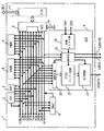
図1には本発明に係るデータプロセッサの一例が示される。同図に示されるデータプロセッサ1は、単結晶シリコンのような1個の半導体チップ若しくは半導体基板に例えばCMOS集積回路製造技術によって形成され、特に制限されないが、RISCプロセッサとしての縮小命令セット(例えば16ビット固定長命令セット)が適用されるCPU(中央処理装置)2と、演算とデータのロード・ストアを並列に実行することによって積和演算を高速に実行可能なDSP3を有する。更にSRAMなどによって構成されるデータメモリ(XMEM,YMEM)4,5、バスステートコントローラ(BSC)6、IOポートなどの入出力回路(I/O)7、DMAC(ダイレクト・メモリ・アクセス・コントローラ)8、デバッグ支援モジュール(AUD)9を有する。CPU2は、特に制限されないが、パイプライン処理によって命令を実行し、見掛け上、CPU2の動作基準クロック信号の1サイクル毎に1命令を実行していくことができる。
【0026】
データプロセッサ1の内部バスは機能毎に複数種類に大別され、情報伝達経路としてそれぞれアドレス及びデータを伝達するIバス(CPUアドレスバスIAB,CPUデータバスIDB)、Xバス(XMEMアドレスバスXAB,XMEMデータバスXDB)、Yバス(YMEMアドレスバスYAB,YMEMデータバスYDB)及びDバス(DMAアドレスバスDAB,DMAデータバスDDB)と、バスアクセス制御情報を伝達するICバス(CPUコマンドバスICMDB)及びDCバス(DMAコマンドバスDCMDB)を有する。
【0027】
前記CPU2は、フェッチした命令を命令デコーダ(図示せず)でデコードし、デコード結果に従って汎用レジスタや算術論理演算器(図示せず)を用いてアドレス情報やデータ情報の演算を行う。このCPU2はアドレスバスIAB、XAB、YABにアドレスを出力可能であり、データバスIDBを介してデータ入出力可能であり、コマンドバスICMDBにバスアクセス制御情報(バスコマンド)を出力可能である。バスコマンドは、リード/ライトの区別、データアクセス/命令フェッチの区別、データサイズ等を指定する情報を含む。
【0028】
前記DSP3は、夫々図示を省略するDSP命令を解読するデコーダ、乗算器、算術論理演算器(ALU)、積和演算専用のデータレジスタファイル等を有する。特に制限されないが、DSP3の演算に必要なデータのアクセス制御はCPU2が行う。DSP3はCPU2のアクセス制御によってデータメモリ(XMEM,YMEM)4,5から読み出されたデータを入力してディジタル信号処理演算を行い、DSP3から出力される演算結果データはCPU2のアクセス制御によってメモリ(XMEM,YMEM)4,5などに格納される。要するに、前記DSP3はデータバスIDB、XDB、YDBを介してデータ入出力可能であり、コマンドバスICMDB及びDCMDBを介してバスアクセス制御情報(バスコマンド)を入力可能である。
【0029】
前記XMEM4及びYMEM5は、SRAM或いはDRAMなどによって構成され、DSP3のデータメモリ或いはCPU2のワークメモリして利用される。前記XMEM4は、アドレスバスIAB、XAB及びDABからアドレス入力可能であり、データバスIDB、XDB及びDDBとの間でデータ入出力入力可能であり、コマンドバスICMDB及びDCMDBを介してバスアクセス制御情報(バスコマンド)を入力可能である。前記YMEM5は、アドレスバスIAB、YAB及びDABからアドレス入力可能であり、データバスIDB、YDB及びDDBとの間でデータ入出力入力可能であり、コマンドバスICMDB及びDCMDBを介してバスアクセス制御情報(バスコマンド)を入力可能である。
【0030】
前記DMAC8はアドレスバスIAB及びデータバスIDBを介してCPU21より転送制御条件の設定が可能にされ、アドレスバスDABにアドレス出力を行い、データバスDDBを利用して、データプロセッサ1の内部で、或いはデータプロセッサ1の内部と外部との間でデータ転送制御を行う。
【0031】
前記BSC6は、CPU2のアクセス動作又はDMAC8によるデータ転送制御に応答して、外部バス11に対する外部バスアクセス、周辺バス10を介する図示を省略する周辺回路アクセスのために、必要なバスサイクルの起動を制御する。DMAC8によるデータ転送先又は転送元がデータプロセッサ1内部の回路モジュールである場合に、それら内部回路モジュールが必要とするバスコマンドはDMAC8からのDMAリクエストに応答してBSC6がコマンドバスDCMDBに出力する。
【0032】
前記デバッグ支援モジュール9は、選択回路20、FIFOバッファ回路21、出力回路22、そして制御回路を構成する制御部23と制御レジスタ部24を有する。前記選択回路20は、前記Iバス(IAB,IDB)、Xバス(XAB,XDB)、Yバス(YAB,YDB)、及びDバス(DAB,DDB)に接続され、トレース条件で指示されたバスを選択し、選択したバス上にトレース条件で指示されたアクセス態様が出現したとき、そのアクセス態様に係る当該バス上の情報を選択する。前記トレース条件によるバスの指定は並列的に複数可能である。前記FIFOバッファ回路21は前記選択回路20で選択された情報(トレース情報)と共に当該情報の属性情報を保持する。属性情報は例えばトレース情報が伝達されたバスの識別情報である。出力回路22は、前記FIFOバッファ回路21に保持されたトレース情報とその属性情報とを所定のフォーマットのパケットデータとしてデータプロセッサ1の外部に直列的に出力可能にする。特に制限されないが、その直列出力データAUDATAは4ビット単位のデータである。制御レジスタ部24はCPU2によりIバス(IAB,IDB)を介してトレース条件が設定される。制御部23は、コマンドバスICMDB,DMDBを介して前記CPU2等の回路モジュールによる動作状態をモニタし、制御レジスタ部24に設定されたトレース条件とモニタした動作状態とに基づいて、前記選択回路20、FIFOバッファ回路21及び出力回路22の動作を制御する。制御部23は前記データAUDATAの4ビット単位の出力が同期されるクロック信号AUDCKと、パケット毎の同期信号AUDSYNCとをデータプロセッサ1の外部に出力する。
【0033】
前記デバッグ支援モジュール9は例えばデータプロセッサ1にデバッグモードが設定されて動作可能にされる。そのようなデバッグモードは、デバッグ対象とされるターゲットシステムにデータプロセッサ1を接続して当該データプロセッサ1にターゲットプログラムを実行させるときに設定すればよい。データプロセッサ1がターゲットプログラムを実行している時、データプロセッサ1の外部に接続されたエミュレータは、前記デバッグ支援モジュール9から出力されるトレース情報とその属性情報をモニタすることができる。このように、デバッグ支援モジュール9の作用により、データプロセッサ1の複数種類の内部バス(Iバス、Xバス、Yバス、Dバス)を外部でモニタ可能であって、モニタしているバスの種別も識別可能である。また、トレース情報とその属性情報は直列的に外部に出力されるから、それら情報をデータプロセッサ1の同一外部端子から出力でき、パッケージの外部端子数の制約から当該デバッグ支援機能が実装不可能になる事態を低減することができる。
【0034】
図2にはデータプロセッサの別の例が示される。同図に示されるデータプロセッサ1Aは、図1に対してマルチCPUの構成を備える。すなわち、第2のCPU12を有し、当該CPU12はCPUアドレスバスI2AB、CPUデータバスI2DB、CPUコマンドバスI2CMDBを介してBSC6に接続される。このとき、選択回路20にはバスI2AB,I2DBも接続され、そのバスI2AB,I2DBからの入力情報もモニタ可能にされる。この構成における属性情報として、更に、バスにトレース情報を出現させる動作がマルチCPU2,12の何れのCPUの動作に基づくかを識別可能にするCPU識別情報を含めておくことが望ましい。制御部23はコマンドバスI2CMDBの情報を入力することにより、トレース条件で指定されたバスI2AB,I2DB上でのアクセス態様の出現も監視する。その他の構成は図1と同様であり、マルチCPU構成においても上記同様の作用及び効果を得る。
【0035】
《パケットデータフォーマット》
図3には図1の出力回路22から出力される前記パケットデータのフォーマットが例示される。前記パケットデータはCMD1,CMD1E,CMD2で表現される属性情報と、これに続くトレース情報とを有する。CMD1はアクセスの種類等を示す4ビットのコードデータである。この例ではトレース条件とされるアクセスの種類は、CPU2による命令実行の分岐をトレース条件とするときの分岐トレース(BPC)、リードアクセス(WDRM)、及びライト(ストア)アクセス(WDWM)に大別され、夫々に固有のコードが割当てられる。分岐トレースをトレース条件とするときトレース情報は分岐元アドレス情報又は/及び分岐先アドレス情報とされる。リードアクセス又は/及びライトアクセスをトレース条件とするときトレース情報はアクセスアドレス情報及びアクセスデータとされる。尚、ここでは、分岐トレースは前記CPU2による分岐命令の実行による分岐を対象とする。割り込みや例外の発生による分岐を対象とすることも可能である。
【0036】
CMD1Eはバスの種類を示す4ビットのコードである。分岐トレースの場合にはトレースすべき分岐先/分岐元のアドレス情報はアドレスバスIAB経由で取得されるだけであるからコードCMD1Eは省かれる。リードアクセス又は/及びライトアクセスの場合、1ビットのプロセッサ識別情報ptと、3ビットのバスの識別情報btを有する。バスの識別情報btはその値に応じて、Iバストレース、Yバストレース、Xバストレース、X及びYバス双方トレース、Dバストレースを示す。
【0037】
CMD2は情報サイズを示す4ビットのコードである。分岐トレース(BCP)コードに続く場合、sdaは2ビットで分岐先アドレスのサイズを示し、ssaは2ビットで分岐元アドレスのサイズを示す。アドレス情報に対しては後述の圧縮処理が施されて出力されるので、sda/ssaの値に応じて、アドレス情報の下位4ビット出力、下位8ビット出力、下位16ビット出力、32ビットフルアドレス出力を示す。ストアアクセス(WDWM)コード又はリードアクセス(WDRM)コードに続く場合、saは2ビットでソースアドレスのサイズを示し、sdは2ビットでデータサイズを示す。アドレス情報は後述の圧縮処理を経て出力されるので、saの値に応じて、アドレス情報の下位4ビット出力、下位8ビット出力(btでX及びYバス双方トレースが指示されている場合には、X,Y夫々下位4ビット出力)、下位16ビット出力(btでX及びYバス双方トレースが指示されている場合には、X,Y夫々下位8ビット出力)、32ビットフルアドレス出力を示す。データサイズはsdの値に応じて8ビット、16ビット、32ビット(btでX及びYバス双方トレースが指示されている場合には、X,Y夫々16ビット出力)を示す。
【0038】
前記コードデータCMD1は、前記分岐トレース(BPC)、リードアクセス(WDRM)、及びライトアクセス(WDWM)の他に、スタンバイ状態(STDBY)及びデータロスト状態(LOST)を示すコードが割り当てられている。STDBYコードはデバッグ支援モジュール9がスタンバイ状態であることを示し、後続データが無いことを意味する。LOSTコードは、前記FIFOバッファ回路21のフル状態によってトレースすべき情報がFIFOバッファ回路21に保持されずに失われたことを示す。これにより、トレースすべき情報の欠落を外部で容易に把握する事が可能になる。トレースすべき情報の欠落を抑制するには、制御部23はFIFOバッファ回路21のフル状態に応答してCPU2やDMAC8による新たなバスアクセスをバスサイクル単位で一時的に停止させる指示を与えるようにすればよい。要するにFIFOバッファ回路21の記憶領域が空くまでCPU2やDMAC8によるバスアクセスをストールさせればよい。
【0039】
《AUD用制御レジスタ》
図4には図1のデバッグ支援モジュール9の詳細な一例が示される。前記制御部23は入力バス制御部30、FIFO制御部31、出力制御部32及びバスストール制御部33を有する。前記出力回路22は、アドレスデータ圧縮部35、パケット変換部36、属性情報生成部37及びデマルチプレクサ38を有する。制御レジスタ部24は制御レジスタ39A,39Bとアドレスデコーダ40とを有する。
【0040】
前記制御レジスタ39A,39Bは図5に例示されるように夫々16ビットのレジスタで構成され、CPU2のアドレス空間に配置され、そのアドレスがアドレスバスIABからアドレスデコーダ40に供給されることによって、データバスIDBを介してリード・ライト可能にされる。前記制御レジスタ39A、39Bの各ビットの意義は図6及び図7に例示される。
【0041】
図6に例示されるように、分岐トレース機能ビットBRE,BRはその設定値にしたがって、分岐トレース無効、分岐トレース有効で分岐元及び分岐先アドレス出力、分岐トレース有効で分岐元アドレスのみ出力、分岐トレース有効で分岐先アドレスのみ出力を指示する。
【0042】
また、分岐トレース以外のトレース条件は、同時に2種類指定(ウインドウAデータトレース、ウインドウBデータトレース)できるようにされ、一方の情報トレース(ウインドウAデータトレース)は、図6のウインドウデータトレース機能ビットWA1,WA0による指定と、図7のウインドウA用プロセッサ別トレースバスセレクト機能ビットWA0B2,WA0B1,WA0B0による指定で決まる。前者の機能ビットWA1,WA0はその値にしたがって、ウインドウAデータトレース機能無効、ウインドウAデータトレースのライトアクセスのみ有効、ウインドウAデータトレースのリードアクセスのみ有効、ウインドウAデータトレースのライト及びリードアクセス有効を指示する。機能ビットWA0B2,WA0B1,WA0B0はその値に従ってウインドウAデータトレース対象バスとしてIバス、Xバス、Yバス、Dバスの中から一つを指定する。他方の情報トレース(ウインドウBデータトレース)は、図6のウインドウデータトレース機能ビットWB1,WB0による指定と、図7のウインドウB用プロセッサ別トレースバスセレクトビットWB0B2,WB0B1,WB0B0による指定で決まる。前者の機能ビットWB1,WB0はその値にしたがって、ウインドウBデータトレース機能無効、ウインドウBデータトレースのライトアクセスのみ有効、ウインドウBデータトレースのリードアクセスのみ有効、ウインドウBデータトレースのライト及びリードアクセス有効を指示する。機能ビットWB0B2,WB0B1,WB0B0はその値に従ってウインドウBデータトレース対象バスとしてIバス、Xバス、Yバス、Dバスの中から一つを指定する。
【0043】
プロセッサコアセレクトビットPT0は図1ではCPUが1個であるから値1に固定とされる。図2の例ではPT0=0でCPU12、PT0=1でCPU2を指定するようにしてよい。或いはPT0=0でCPU2、PT0=1でCPU2及びCPU12を指定するようにしてもよい。
【0044】
図6に示されるトレースモードビットTMはその値によってフルトレースモード又はリアルタイムトレースモードを指定する。フルトレースモードでは全てのトレース情報を出力するモードであり、FIFOバッファ回路21がフル状態になれば、空きができるまでバスストール制御部33にてCPU2をストールさせる。リアルタイムトレースモードはCPU2を停止させること無くリアルタイムでトレース情報を出力するモードであり、FIFOバッファ回路21がフル状態になったり、ウインドウA,Bで並列してトレース情報が発生したりするとき、属性情報生成部37が前記LOSTコードを発行することになる。
【0045】
《選択回路》
図8には前記選択回路の一例が示される。同図に示される選択回路20は、第1セレクタ(ウインドウAセレクタ)41、第2セレクタ(ウインドウBセレクタ)42、第3セレクタ43、及び命令アドレスバッファ44を有する。第1セレクタ41は、Iバス(IAB,IDB)、Xバス(XAB,XDB)、Yバス(YAB,YDB)、Dバス(DAB,DDB)の中からトレースすべき情報を得るためのバスを選択すると共に選択したバスの情報をバスサイクル単位で保持する。前記第2セレクタ42も同じく、Iバス(IAB,IDB)、Xバス(XAB,XDB)、Yバス(YAB,YDB)、Dバス(DAB,DDB)の中からトレースすべき情報を得るためのバスを選択すると共に選択したバスの情報をバスサイクル単位で保持する。命令アドレスバッファ44はCPU2が現在実行中の命令アドレスの直前の命令の命令アドレスを保持する。要するに、命令アドレスバッファ44はIバスのアドレスバスIABに伝達される命令アドレスを入力し、次の命令アドレスが入力された後も当該次の命令が実行完了されるまでの所定期間保持する。前記第3セレクタ43は、前記第1セレクタ41、前記第2セレクタ42及び前記命令アドレスバッファ44の出力から一つを選択して前記FIFOバッファ回路21に与える。
【0046】
このとき、前記入力バス制御部30は、制御レジスタ39BのウインドウA用プロセッサコア別トレースバスセレクトビットWA0B2,WA0B1,WA0B0によって指定されるバスの選択信号45Aを第1セレクタ41に与える。同様に、前記入力バス制御部30は、制御レジスタ39BのウインドウB用プロセッサコア別トレースバスセレクトビットWB0B2,WB0B1,WB0B0によって指定されるバスの選択信号45Bを第2セレクタ42に与える。前記第3セレクタ43に対して入力バス制御部30は、制御レジスタ39Aの分岐トレース機能ビットBRE,BR、ウインドウデータトレース機能ビットWA1,WA0,WB1,WB0によって指定されたアクセス態様の出現に応じ、前記第1セレクタ41、前記第2セレクタ42又は前記命令アドレスバッファ44の出力を選択させ選択信号46を出力する。トレース条件として指定されたアクセス態様が出現したか否かはコマンドバスICMDB,DCMDBの状態を監視して判定すればよい。例えば、第1セレクタ41で選択されているバス上においてトレース条件で指定されたアクセス態様が出現したとき、入力バス制御部30は第3セレクタ43に当該第1セレクタ41の出力を選択させる。また、第2セレクタ42で選択されているバス上においてトレース条件で指定されたアクセス態様が出現したとき、入力バス制御部30は第3セレクタ43に当該第2セレクタ42の出力を選択させる。また、入力バス制御部30は、分岐トレースが有効に指示されているとき、分岐命令の実行を検出すると、分岐先命令である次の命令アドレスがアドレスバスIABから第1セレクタ41に入力された後、第3セレクタ43に、命令アドレスバッファ44が保持する分岐元命令アドレスと、第1セレクタ41が保持する分岐先アドレスとをFIFOバッファ回路21に供給させる。
【0047】
上記選択回路20により、第1セレクタ41及び第2セレクタ42で選択される夫々の内部バスの状態を並列的にモニタすることができる。このとき、並列モニタ可能な複数のバス上でトレース対象とされるアクセス態様が同一バスサイクルで出現することがある。入力バス制御回路30は、フルトレースモードが指定されている状態において、前記第1セレクタ41及び第2セレクタ42で選択される夫々のバスにおいてトレース条件で指定されたアクセス態様が同一バスサイクルで出現したとき、バスストール制御部33にCPU2による命令実行又はDMACによるデータ転送動作を一時停止させ、夫々のアクセス態様で双方のバスに出現し前記第1及び第2セレクタ41,42に保持されたトレース情報を第3セレクタ43を介して直列的にFIFOバッファ回路21に格納させる。
【0048】
《バスストール制御》
ここで図4を参照しながらバスストール制御について詳述する。入力バス制御部30はコマンドバスICMDB,DCMDBからのバスコマンドに基づいてトレース条件に一致する状態が出現したかを判定しており、トレース条件に一致する状態の発生をヒット信号HITa,HITb,HITiとして出力する。ヒット信号HITaはウインドウAデータトレースの条件に一致したとき(第1及び第3セレクタ41,43経由でトレースデータが取得されるとき)活性化され、ヒット信号HITbはウインドウBデータトレースの条件に一致したとき(第2及び第3セレクタ42,43経由でトレースデータが取得されるとき)活性化され、ヒット信号HITiはCPU2による命令実行に分岐を生じた時活性化される。入力バス制御部30はヒット信号HITa,HITb,HITiが活性化されるとき、信号53によってFIFO制御部31に書込みリクエストを行う。
【0049】
FIFO制御部31はFIFOバッファ回路21に対して先入れ先出し形式でデータのリード・ライトを制御する。ライト可能な記憶エリアがなくなった時フル信号50を活性化し、リード可能なデータが無くなった時エンプティ信号51を活性化する。FIFI制御回路31に対するリードリクエストは信号52で与えられる。
【0050】
バスストール制御部33には前記ヒット信号HITa,HITb,HITi、フル信号50、及び制御レジスタ39A,39Bの設定データが入力される。バスストール制御部33は、トレースモードビット(TM)によりフルトレースモードが指示されているとき、フル状態のときに前記ヒット信号HITa,HITb,HITiが活性化された時、Iバス用のバスレディー信号AUDIRDY又はDバス用のバスレディー信号AUDDRDYを非活性化する。この例に従えば、バスレディー信号AUDIRDY,AUDDRDYはBSC6に供給され、バスレディー信号AUDIRDYの非活性化によりIバスを利用するバスアクセスが抑止され、バスレディー信号AUDDRDYの非活性化によりDバスを利用するバスアクセスが抑止される。
【0051】
《LOSTフラグ制御》
前記バスストール制御部33は、特に図示はしないが、トレースモードビット(TM)によりリアルタイムトレースモードが指示されている場合、FIFOバッファ回路21がフル状態のときに前記ヒット信号HITa,HITb,HITiが活性化される毎に入力バス制御部30内のLOSTフラグを順次セット状態として保持させる。その後、FIFOバッファ回路21に最初の空きが生じたとき、入力バス制御部30はLOSTフラグのセット数の情報をFIFO制御部31を介してFIFOバッファ回路21に書き込み制御する。
【0052】
《出力制御》
ここで図4を参照しながら出力回路22による出力制御について詳述する。入力バス制御部30はコマンドバスICMDB,DCMDBから入力されるバスコマンドの内容を解読して、属性情報として利用するバスアクセス制御情報をバスサイクル毎に取得し、FIFOバッファ回路21に与える。FIFIバッファ回路21はトレースすべきアドレス情報やデータ情報などと一緒に、対応するバスアクセス制御情報を、例えば同じFIFO記憶段に記憶する。FIFOバッファ回路21に対する書込みの指示は前記信号53によって与えられる。FIFOバッファ回路21に対する読み出しは信号52で指示する。
【0053】
属性情報生成部37は、FIFOバッファ回路21から読み出されたバスアクセス制御情報を入力し、制御レジスタ39A,39Bの設定値を受ける出力制御部32の制御に従って、図3で説明したCMD1,CMD1E,CMD2で表される形態で属性情報を生成する。アドレスデータ圧縮部35はFIFOバッファ回路21から読み出されたトレースすべき情報としてのアドレス情報を圧縮処理して出力する。
【0054】
アドレス情報の圧縮は、図9に例示されるように、直前のアドレス情報との差分を出力するという手法によって行う。すなわち、図9の(A),(B)に例示されるように、全ビット一致のとき、或いは下位4ビットの範囲内で不一致の時には、今回のアドレス情報の下位4ビットだけを出力対象とする。(C)のように第5ビット目から第8ビット目の範囲で不一致ビットがあれば今回のアドレス情報の下位8ビットだけを出力対象とする。(D)のように第9ビット目から第16ビット目の範囲で不一致ビットがあれば今回のアドレス情報の下位16ビットだけを出力対象とする。(E)のように第17ビット目から第32ビット目の範囲で不一致ビットがあれば今回のアドレス情報をフルアドレスで出力対象とする。パケット変換部36は出力制御部32の制御にしたがって、図3で説明したパケットデータフォーマットに従ってアドレス情報やデータ情報のフォーマット変換を行う。
【0055】
出力制御部32はクロック信号AUDCKに同期させて、前記CMD1,CMD1E,CMD2で表現される属性情報と、パケット変換部36から出力されるトレース情報を、デマルチプレクサ39で所定の順番に選択して、モニタデータAUDATAとして外部に出力させ、パケット毎にパケット同期信号AUDSYNCを変化させる。
【0056】
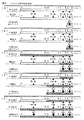
図10及び図11には分岐トレース(BPC)時におけるデータAUDATA、クロック信号AUDCK、パケット同期信号AUDSYNCの出力例が示される。図10はMD2の後にDAとして分岐先アドレス情報が16ビット、SAとして分岐元アドレス情報が8ビット続いている。図11ではMD2の後にSAとして分岐元アドレス情報が8ビット続いている。
【0057】
図12にはライトアクセス(WDWM)時におけるデータAUDATA、クロック信号AUDCK、パケット同期信号AUDSYNCの出力例が示される。MD2の後にAとしてアドレス情報が16ビット、Dとしてデータ情報が16ビット続いている。
【0058】
図13にはライトアクセス(WDWM)時におけるウインドウA,Bの連続トレース時におけるデータAUDATA、クロック信号AUDCK、パケット同期信号AUDSYNCの出力例が示される。前後2回の出力動作では、MD2の後にAとしてアドレス情報が16ビット、Dとしてデータ情報が16ビット続いている。
【0059】
図14にはリアルタイムトレースにおいてトレースデータ取りこぼしを生ずるときのデータAUDATA、クロック信号AUDCK、パケット同期信号AUDSYNCの出力例が示される。データの取りこぼしを生じているとき、LOSTコードが出力され、LOSTコードの出力によってパケット同期信号AUDSYCKがローレベルにされ、次のBPCコードが出力された時は既にパケット同期信号AUDSYCKがローレベルにされている。LOST状態の後のパケット出力はパケット同期信号AUDSYCKによっても他のパケット出力と区別可能になる。前記LOSTコードはFIFOバッファ回路21に格納されているところの前記LOSTフラグのセット数の情報に基づいて属性情報生成部37が生成する。
【0060】
《バスとFIFOバッファ回路との接続形態》
図15には選択回路20によるIバスとFIFOバッファ回路の接続形態が模式的に例示される。バスIAB,IDBは夫々32ビットである。FIFOバッファ回路21の一つの記憶段はここでは74ビットとされ、32ビットのアドレス記憶エリアE1,32ビットのデータ記憶エリアE2、及び10ビットの属性情報エリアE3が割当てられている。
【0061】
図16には選択回路20によるXバス、YバスとFIFOバッファ回路の接続形態が模式的に例示される。Xバス、YバスはIバスに比べてビット数が半分以下にされている。特に制限されないが、アドレスバスXAB,YABは夫々15ビット、XDB,YDBは夫々16ビットとされる。FIFOバッファ回路21の一つの記憶段は74ビットとされ、図15と同じように、32ビットのアドレス記憶エリアE1,32ビットのデータ記憶エリアE2、及び10ビットの属性情報エリアE3が割当てられている。但し、アドレスエリアE1には2種類のアドレスバスXAB,YABが上位及下位の記憶エリアに並列的に接続され、データエリアE2には2種類のデータバスXDB,YDBが上位及下位の記憶エリアに並列的に接続される。したがって、Xバス(XAB,XDB)及びYバス(YAB,YDB)をトレース対象とし、トレース条件に一致するアクセス状態が双方のバスに並行して出現した場合、双方のトレース情報を一度にFIFIバッファ回路21に格納することができる。したがってその場合には、リアルタイムトレースモードにおいてはトレース情報が失われず、フルトレースモードではバスストールが発生しない。
【0062】
《バス以外からのトレース情報》
以上の説明ではトレース情報はアドレスバス及びデータバスから取得するものとして説明した。図17にはバス以外からトレース情報を取得可能にするデータプロセッサ1Bの構成が概略的に例示される。例えばタイマやシリアルインタフェースなどのその他の回路モジュール60,61から内部ステートなどのトレースしたい信号が伝達される信号線62,63を前記選択回路に接続する。制御部23にはトレースすべき信号の発生(トレースイベント)を定義する信号例えば割込み信号等を信号線64,65から入力する。これにより、バスアクセス以外の所望のトレースイベントの発生に応答して、対応するイベント発生情報をトレース情報としてFIFOバッファ回路に蓄えることができる。この場合も、上記同様、複数のバスやトレースイベントを並列的に監視してトレース情報を取得でき、それらを少ない数の外部端子からデータAUDATAとして直列的に外部に出力することができる。
【0063】
以上本発明者によってなされた発明を実施形態に基づいて具体的に説明したが、本発明はそれに限定されるものではなく、その要旨を逸脱しない範囲において種々変更可能であることは言うまでもない。
【0064】
例えば、その他の回路モジュールはDSPやメモリに限定されず適宜変更可能である。情報伝達経路としてのバスの構成は上記Iバス、Xバス、Yバス、Dバスに限定されず、内蔵回路モジュールの種類などに応じて適宜変更可能である。また、トレース情報を出力するパケットのフォーマットやコードデータの種類、制御レジスタの設定値の意義などについても適宜変更可能である。図8の構成は並列的に2種類のバスを指定してトレース可能にするが、並列的に3種類以上のバスを指定する構成を採用してもよい。また、トレース情報としてのアドレス情報は圧縮処理を一切施さずに、常にフルアドレスで出力してもよい。
【0065】
【発明の効果】
本願において開示される発明のうち代表的なものによって得られる効果を簡単に説明すれば下記の通りである。
【0066】
すなわち、データプロセッサの外部ではトレースすべき情報とその属性情報とを対にしてモニタ可能になるから、複数種類の内部バスのような情報伝達経路を外部でモニタ可能であって夫々モニタしている情報伝達経路を識別可能である。また、トレース情報とその属性情報は直列的に外部に出力されるから、それら情報を同一外部端子から出力でき、パッケージの外部端子数の制約から当該デバッグ支援機能が実装不可能になる事態を低減することができる。
【0067】
また、複数の情報伝達経路の中からトレース条件に従って複数の情報伝達経路を選択し、選択した情報伝達経路からトレース条件に従ってトレース情報を取得するようにすれば、複数種類の情報伝達経路を並列的に外部でモニタすることができる。
【図面の簡単な説明】
【図1】本発明に係るデータプロセッサの第1の例を示すブロック図である。
【図2】本発明に係るデータプロセッサの第2の例としてCPUを複数有するものを示すブロック図である。
【図3】図1の出力回路から出力される前記パケットデータのフォーマットを説明するための説明図である。
【図4】図1のデータプロセッサに内蔵されるデバッグ支援モジュールの詳細な一例を示すブロック図である。
【図5】制御レジスタの制御ビット構成を例示する説明図である。
【図6】制御レジスタの制御ビットの定義を示す説明図である。
【図7】制御レジスタの制御ビットの定義を示す説明図である。
【図8】図4のデバッグ支援モジュールが有する選択回路の詳細を例示するブロック図である。
【図9】アドレス情報の圧縮処理方法を例示する説明図である。
【図10】分岐トレース(BPC)時におけるデータAUDATA、クロック信号AUDCK、パケット同期信号AUDSYNCの第1の出力例を示すタイミングチャートである。
【図11】分岐トレース(BPC)時におけるデータAUDATA、クロック信号AUDCK、パケット同期信号AUDSYNCの第2の出力例を示すタイミングチャートである。
【図12】ライトアクセス(WDWM)時におけるデータAUDATA、クロック信号AUDCK、パケット同期信号AUDSYNCの出力例を示すタイミングチャートである。
【図13】ライトアクセス(WDWM)時におけるウインドウA,Bの連続トレース時におけるデータAUDATA、クロック信号AUDCK、パケット同期信号AUDSYNCの出力例を示すタイミングチャートである。
【図14】リアルタイムトレースにおいてトレースデータ取りこぼしを生ずるときのデータAUDATA、クロック信号AUDCK、パケット同期信号AUDSYNCの出力例を示すタイミングチャートである。
【図15】選択回路によるIバスとFIFOバッファ回路との接続形態を模式的に例示するブロック図である。
【図16】選択回路によるXバス、YバスとFIFOバッファ回路との接続形態を模式的に例示するブロック図である。
【図17】バス以外からトレース情報を取得可能にするデータプロセッサを例示する概略ブロック図である。
【符号の説明】
1 データプロセッサ
2 CPU
3 DSP
4 Xデータメモリ(XMEM)
5 Yデータメモリ(YMEM)
6 バスステートコントローラ(BSC)
8 DMAC
9 デバッグ支援モジュール(AUD)
IAB、IDB Iバス
XAB,XDB Xバス
YAB,YDB Yバス
DAB,DDB Dバス
DCMDB DCバス
ICMDB ICバス
20 選択回路
21 FIFOバッファ回路
22 出力回路
23 制御部
24 制御レジスタ部
30 入力バス制御部
31 FIFOI制御部
32出力制御部
33 バスストール制御部
41 第1セレクタ
42 第2セレクタ
43 第3セレクタ
44 命令アドレスバッファ
50 フル信号
51 エンプティ信号
52 リードリクエスト信号
53 ライトリクエスト信号
AUDATA パケットデータ
AUDCK クロック信号
AUDSYNC パケット同期信号
AUDIRDY Iバスレディー信号
AUDDRDY Dバスレディー信号[0001]
BACKGROUND OF THE INVENTION
The present invention relates to a semiconductor processor integrated data processor, and more particularly to a debugging support function in a data processor, for example, a technique effective when applied to traces for a plurality of types of internal buses built in the data processor.
[0002]
[Prior art]
A data processor such as a microcomputer is equipped with other circuit modules together with a CPU. However, the number of built-in circuit modules has increased due to the demand for higher functionality, and the configuration of the internal bus has become complicated accordingly. When debugging a system using a data processor, it is necessary to monitor the internal state of the data processor while executing the target program, and use it for debugging. However, in situations where the data processor's circuit configuration and bus configuration are complicated It has been found by the present inventor that it becomes difficult to monitor internal information of various internal buses while executing a target program, and to monitor the bus information in real time or in a state close to this.
[0003]
As literatures focusing on the internal data trace function in the data processor, there are JP-A-11-219303 and JP-A-3-90955 which describe a multiprocessor tracing method. The former document does not consider the viewpoint of monitoring a plurality of buses and the viewpoint of adding processor identification information to trace information. The latter document exemplifies a viewpoint of using identification information indicating from which CPU the bus information is from.
[0004]
[Problems to be solved by the invention]
However, the latter document does not take into consideration the monitor for a plurality of buses. In short, no attention has been paid to the function of enabling monitoring of data of a plurality of buses in parallel and identifying the bus being monitored. Further, in the latter document, bus information and identification information are output in parallel from dedicated terminals, and assuming that the information is output from a one-chip data processor, it cannot be realized due to restrictions on the number of external terminals. It is expected that there are cases where
[0005]
An object of the present invention is to provide a data processor having a debugging support function capable of monitoring a plurality of types of internal buses externally and identifying the buses being monitored.
[0006]
Another object of the present invention is to provide a data processor having a debugging support function capable of externally monitoring a plurality of types of internal buses in parallel.
[0007]
Another object of the present invention is to provide a data processor having a debugging support function capable of outputting information to be traced and identification information enabling identification of a route through which the information is transmitted from the same external terminal.
[0008]
The above and other objects and novel features of the present invention will be apparent from the description of this specification and the accompanying drawings.
[0009]
[Means for Solving the Problems]
The following is a brief description of an outline of typical inventions disclosed in the present application.
[0010]
[1] In the data processor according to the first aspect of the present invention, a CPU, a debug support module, and other circuit modules are mounted on a semiconductor chip. The debug support module selects an information transmission path according to a trace condition from a plurality of information transmission paths used for the operation of the CPU or other circuit modules, and trace information obtained according to the trace condition from the selected information transmission path At the same time, the attribute information of the information is held in the buffer circuit, and the trace information and the attribute information held in the buffer circuit can be serially output to the outside of the semiconductor chip in a predetermined format.
[0011]
The attribute information is identification information of an information transmission path, for example, a bus, through which corresponding trace information is transmitted. The attribute information is CPU identification information that makes it possible to identify which CPU of the multi CPU is based on the operation of causing the corresponding trace information to appear in the information transmission path.
[0012]
As described above, since it is possible to monitor the information to be traced and its attribute information outside the data processor, a plurality of types of internal buses can be monitored externally, and the bus being monitored can be identified. is there. In addition, since trace information and its attribute information are serially output to the outside, the information can be output from the same external terminal, reducing the situation where the debug support function cannot be implemented due to restrictions on the number of external terminals in the package can do.
[0013]
[2] As a specific aspect of the debug support function in the data processor, when read access is a trace condition, if the trace information is address information and data information for read access, the attribute information has an access type Information indicating read access, bus identification information indicating the type of information transmission path, and size information indicating the size of information to be traced may be used.
[0014]
When the trace information is address information and data information for write access when the write access is set as a trace condition, the attribute information includes information indicating that the access type is write access, and the type of information transmission path. The bus identification information to be displayed and the size information indicating the size of the information to be traced may be used.
[0015]
Further, when the branch of instruction execution by the CPU (for example, branch by execution of branch instruction by CPU, interruption or exception processing) is set as a trace condition, if the trace information is branch source address information and branch destination address information, The attribute information may be information indicating that a branch is traced, information indicating the size of branch source address information to be traced, and information indicating the size of branch destination address information to be traced.
[0016]
When the branch of instruction execution by the CPU is set as a trace condition, if the trace information is branch source address information, the attribute information indicates information indicating that the branch is traced and the size of the branch source address information to be traced. It may be information. Similarly, if the trace information is branch destination address information at that time, the attribute information may be information indicating that the trace is at the time of branching and information indicating the size of the branch destination address information to be traced.
[0017]
[3] In the data processor according to the second aspect of the present invention, a CPU, a debug support module, and other circuit modules are mounted on a semiconductor chip. The debug support module selects an information transmission path according to a trace condition from a plurality of information transmission paths used for the operation of the CPU or other circuit modules, and acquires trace information from the selected information transmission path according to the trace condition. A selection circuit that holds the attribute information of the information together with the trace information selected by the selection circuit, and the trace information and the attribute information held in the buffer circuit in a predetermined format. The operation of the selection circuit, the buffer circuit, and the output circuit is controlled based on an output circuit that enables serial output to the outside, a trace condition specified by the CPU, and an operation state by the CPU and other circuit modules. And a control circuit.
[0018]
Even in a data processor according to this point of view, it is possible to monitor a pair of trace information and its attribute information externally, so it is possible to monitor a plurality of types of internal buses externally and identify the buses being monitored. In addition, information to be traced and its attribute information can be output from the same external terminal.
[0019]
[4] If the buffer circuit in the data processor according to the second aspect is a FIFO buffer circuit, it is not necessary to consider the address space of the CPU for information storage. At this time, the control circuit may output an information code indicating that the information to be traced is lost without being held in the buffer circuit due to the full state of the FIFO buffer circuit from the output circuit to the outside of the semiconductor chip. As a result, it is possible to easily grasp the lack of information to be traced outside. In order to suppress the lack of information to be traced, the control circuit may give an instruction to temporarily stop a new bus access operation in units of bus cycles in response to the full state of the FIFO buffer circuit. In short, bus access by the CPU or DMAC may be stalled until the storage area is free in the FIFO buffer circuit.
[0020]
[5] In the selection circuit in the data processor according to the second aspect, for example, an information transmission path for obtaining trace information is selected from a plurality of information transmission paths, and information on the selected information transmission path is stored in bus cycle units. A first selector that holds information, a second selector that selects information transmission paths for obtaining trace information from a plurality of information transmission paths, and holds information on the selected information transmission paths in units of bus cycles, and a current execution An instruction address buffer for holding the instruction address of the instruction immediately before the instruction address therein, and a third selector for selecting one from the outputs of the first selector, the second selector, and the instruction address buffer and giving it to the buffer circuit The structure which has is adopted. At this time, the control circuit causes the first and second selectors to select the information transmission path specified by the trace condition, and the third selector selects the first selector according to the appearance of the access mode specified by the trace condition. The output of the second selector or the instruction address buffer is selected.
[0021]
As a result, the states of the plurality of internal buses selected by the first selector and the second selector can be monitored in parallel.
[0022]
In order to cope with the case where the access mode to be traced appears in the same bus cycle on a plurality of buses that can be monitored in parallel, the control circuit transmits each information selected by the first selector and the second selector. When the access mode specified by the trace condition in the path appears in the same bus cycle, a new bus access operation by the CPU or DMAC is temporarily stopped, and appears in both information transfer paths in the respective access modes. The information held in the second selector may be stored in the buffer circuit serially via the third selector.
[0023]
[6] As a more specific mode in the data processor of the second aspect, the other circuit module includes a DSP, an X memory, a Y memory, a DMAC, and a bus state controller, and an address and data are respectively transmitted as the information transmission path. When having an I bus, an X bus, a Y bus, and a D bus for transmitting, and an IC bus and a DC bus for transmitting bus access control information, the CPU can output addresses to the I bus, the X bus, and the Y bus, Data can be input / output via the I bus, and bus access control information can be output to the IC bus. The DSP can input / output data via the I bus, X bus, and Y bus, and the IC bus and DC Bus access control information can be input via a bus, and the X memory can input addresses from the I bus, X bus, and D bus. Data input / output is possible between the I bus, X bus and D bus, and the Y memory can be addressed from the I bus, Y bus and D bus, and the I bus, Y bus and D bus. Data input / output can be input to the bus, bus access control information can be input via the IC bus and DC bus, and the DMAC can set transfer control conditions via the I bus, and the D bus The bus state controller can output bus access control information to the DC bus for access control by the DMAC.
[0024]
At this time, the control circuit is connected to the IC bus and the DC bus, and based on access control information supplied via the IC bus and the DC bus, determines the occurrence of an access operation that matches a trace condition, The selection circuit may select the bus used for the access operation that matches the trace condition.
[0025]
DETAILED DESCRIPTION OF THE INVENTION
<Data processor>
FIG. 1 shows an example of a data processor according to the present invention. The
[0026]
The internal bus of the
[0027]
The
[0028]
The
[0029]
The
[0030]
The
[0031]
In response to the access operation of the
[0032]
The
[0033]
The
[0034]
FIG. 2 shows another example of a data processor. The
[0035]
<Packet data format>
FIG. 3 illustrates a format of the packet data output from the
[0036]
CMD1E is a 4-bit code indicating the type of bus. In the case of the branch trace, the address information of the branch destination / branch source to be traced is only acquired via the address bus IAB, so the code CMD1E is omitted. In the case of read access and / or write access, 1-bit processor identification information pt and 3-bit bus identification information bt are included. The bus identification information bt indicates I bus trace, Y bus trace, X bus trace, both X and Y bus trace, and D bus trace according to the value.
[0037]
CMD2 is a 4-bit code indicating the information size. When following the branch trace (BCP) code, sda indicates the size of the branch destination address with 2 bits, and ssa indicates the size of the branch source address with 2 bits. Since the address information is output after being subjected to compression processing described later, the lower 4 bits output, the lower 8 bits output, the lower 16 bits output, and the 32-bit full address of the address information according to the value of sda / ssa Indicates the output. When following a store access (WDWM) code or a read access (WDRM) code, sa indicates the size of the source address with 2 bits, and sd indicates the data size with 2 bits. Since the address information is output after compression processing described later, according to the value of sa, lower 4 bits output and lower 8 bits output of the address information (when both X and Y bus traces are instructed by bt) , X and Y respectively lower 4 bits output), lower 16 bits output (when both traces X and Y are instructed by bt, lower 8 bits are output X and Y respectively), 32 bits full address output . The data size indicates 8 bits, 16 bits, or 32 bits according to the value of sd (when both the X and Y bus traces are indicated by bt, 16 bits are output for each of X and Y).
[0038]
The code data CMD1 is assigned a code indicating a standby state (STDBY) and a data lost state (LOST) in addition to the branch trace (BPC), read access (WDRM), and write access (WDWM). The STDBY code indicates that the
[0039]
<< AUD control register >>
FIG. 4 shows a detailed example of the
[0040]
The control registers 39A and 39B are each composed of a 16-bit register as illustrated in FIG. 5 and are arranged in the address space of the
[0041]
As illustrated in FIG. 6, the branch trace function bits BRE and BR are output according to the set values of the branch trace disabled, the branch trace enabled, the branch source and destination addresses output, the branch trace enabled, the branch source address output only, the branch The trace is valid and only the branch destination address is output.
[0042]
Further, two types of trace conditions other than the branch trace can be specified simultaneously (window A data trace, window B data trace), and one information trace (window A data trace) is a window data trace function bit of FIG. It is determined by designation by WA1 and WA0 and designation by trace bus select function bits WA0B2, WA0B1 and WA0B0 for each window in FIG. According to the values of the former function bits WA1 and WA0, the window A data trace function is invalid, only the window A data trace write access is valid, only the window A data trace read access is valid, and the window A data trace write and read access are valid. Instruct. The function bits WA0B2, WA0B1, and WA0B0 designate one of the I bus, X bus, Y bus, and D bus as the window A data trace target bus according to the value. The other information trace (window B data trace) is determined by designation by window data trace function bits WB1 and WB0 in FIG. 6 and designation by trace bus select bits WB0B2, WB0B1 and WB0B0 for each window B in FIG. According to the values of the former function bits WB1 and WB0, the window B data trace function is invalid, only the window B data trace write access is valid, only the window B data trace read access is valid, and the window B data trace write and read access are valid. Instruct. Function bits WB0B2, WB0B1, and WB0B0 specify one of the I, X, Y, and D buses as the window B data trace target bus according to the value.
[0043]
The processor core select bit PT0 is fixed at a value of 1 because there is only one CPU in FIG. In the example of FIG. 2, the
[0044]
The trace mode bit TM shown in FIG. 6 designates the full trace mode or the real-time trace mode depending on its value. In the full trace mode, all trace information is output. When the
[0045]
<Selection circuit>
FIG. 8 shows an example of the selection circuit. The
[0046]
At this time, the input
[0047]
The
[0048]
<Bus stall control>
Here, the bus stall control will be described in detail with reference to FIG. The input
[0049]
The
[0050]
The bus
[0051]
<< LOST flag control >>
Although not specifically shown, the bus
[0052]
<Output control>
Here, the output control by the
[0053]
The attribute information generation unit 37 receives the bus access control information read from the
[0054]
The address information is compressed by a method of outputting a difference from the immediately preceding address information as illustrated in FIG. That is, as illustrated in FIGS. 9A and 9B, when all bits match or when there is a mismatch within the lower 4 bits, only the lower 4 bits of the current address information are output. To do. If there is a mismatch bit in the range from the 5th bit to the 8th bit as in (C), only the lower 8 bits of the current address information are output. If there is a mismatch bit in the range from the 9th bit to the 16th bit as in (D), only the lower 16 bits of the current address information are output. As shown in (E), if there is a mismatch bit in the range from the 17th bit to the 32nd bit, the current address information is output as a full address. The
[0055]
The
[0056]
10 and 11 show output examples of data AUDATA, clock signal AUDCK, and packet synchronization signal AUDSYNC at the time of branch trace (BPC). In FIG. 10, after MD2, branch destination address information is 16 bits as DA and branch source address information is 8 bits as SA. In FIG. 11, the branch source address information is followed by 8 bits as SA after MD2.
[0057]
FIG. 12 shows an output example of data AUDATA, clock signal AUDCK, and packet synchronization signal AUDSYNC at the time of write access (WDWM). MD2 is followed by 16 bits of address information as A and 16 bits of data information as D.
[0058]
FIG. 13 shows an output example of the data AUDATA, the clock signal AUDCK, and the packet synchronization signal AUDSYNC when the windows A and B are continuously traced during write access (WDWM). In the two output operations before and after, MD2 is followed by 16 bits of address information as A and 16 bits of data information as D.
[0059]
FIG. 14 shows an output example of the data AUDATA, the clock signal AUDCK, and the packet synchronization signal AUDSYNC when the trace data is lost in the real-time trace. When data is lost, the LOST code is output, and the packet synchronization signal AUDSYCK is set to low level by the output of the LOST code. When the next BPC code is output, the packet synchronization signal AUDSYCK is already set to low level. ing. The packet output after the LOST state can be distinguished from other packet outputs by the packet synchronization signal AUDSYCK. The attribute information generator 37 generates the LOST code based on the information on the number of sets of the LOST flag stored in the
[0060]
<< Connection between bus and FIFO buffer circuit >>
FIG. 15 schematically illustrates a connection form of the I bus and the FIFO buffer circuit by the
[0061]
FIG. 16 schematically illustrates the connection form of the X bus, the Y bus, and the FIFO buffer circuit by the
[0062]
<< Trace information from other than bus >>
In the above description, the trace information is described as being acquired from the address bus and the data bus. FIG. 17 schematically illustrates the configuration of the
[0063]
Although the invention made by the present inventor has been specifically described based on the embodiments, it is needless to say that the present invention is not limited thereto and can be variously modified without departing from the gist thereof.
[0064]
For example, other circuit modules are not limited to DSPs and memories, and can be changed as appropriate. The configuration of the bus as the information transmission path is not limited to the I bus, X bus, Y bus, and D bus, and can be changed as appropriate according to the type of the built-in circuit module. Further, the format of the packet for outputting the trace information, the type of code data, the significance of the set value of the control register, and the like can be changed as appropriate. Although the configuration of FIG. 8 enables tracing by specifying two types of buses in parallel, a configuration in which three or more types of buses are specified in parallel may be employed. Further, the address information as the trace information may be always output as a full address without performing any compression processing.
[0065]
【The invention's effect】
The effects obtained by the representative ones of the inventions disclosed in the present application will be briefly described as follows.
[0066]
That is, since information to be traced and its attribute information can be monitored outside the data processor, information transmission paths such as a plurality of types of internal buses can be monitored externally and monitored respectively. An information transmission path can be identified. In addition, since trace information and its attribute information are serially output to the outside, the information can be output from the same external terminal, reducing the situation where the debug support function cannot be implemented due to restrictions on the number of external terminals in the package can do.
[0067]
In addition, if a plurality of information transmission paths are selected from a plurality of information transmission paths according to the trace conditions, and trace information is acquired from the selected information transmission paths according to the trace conditions, a plurality of types of information transmission paths can be parallelized. Can be monitored externally.
[Brief description of the drawings]
FIG. 1 is a block diagram showing a first example of a data processor according to the present invention.
FIG. 2 is a block diagram showing a second example of a data processor according to the present invention having a plurality of CPUs.
FIG. 3 is an explanatory diagram for explaining a format of the packet data output from the output circuit of FIG. 1;
4 is a block diagram showing a detailed example of a debug support module built in the data processor of FIG. 1;
FIG. 5 is an explanatory diagram illustrating a control bit configuration of a control register.
FIG. 6 is an explanatory diagram illustrating the definition of control bits of a control register.
FIG. 7 is an explanatory diagram illustrating a definition of control bits of a control register.
FIG. 8 is a block diagram illustrating details of a selection circuit included in the debug support module of FIG. 4;
FIG. 9 is an explanatory diagram illustrating a compression processing method for address information;
FIG. 10 is a timing chart showing a first output example of data AUDATA, a clock signal AUDCK, and a packet synchronization signal AUDSYNC during branch trace (BPC).
FIG. 11 is a timing chart showing a second output example of data AUDATA, clock signal AUDCK, and packet synchronization signal AUDSYNC during branch trace (BPC).
FIG. 12 is a timing chart showing an output example of data AUDATA, clock signal AUDCK, and packet synchronization signal AUDSYNC at the time of write access (WDWM);
FIG. 13 is a timing chart showing an output example of data AUDATA, clock signal AUDCK, and packet synchronization signal AUDSYNC during continuous tracing of windows A and B during write access (WDWM).
FIG. 14 is a timing chart showing an output example of data AUDATA, clock signal AUDCK, and packet synchronization signal AUDSYNC when a trace data dropout occurs in a real-time trace.
FIG. 15 is a block diagram schematically illustrating a connection form between an I bus and a FIFO buffer circuit by a selection circuit;
FIG. 16 is a block diagram schematically illustrating a connection form between an X bus and a Y bus and a FIFO buffer circuit by a selection circuit;
FIG. 17 is a schematic block diagram illustrating a data processor that enables acquisition of trace information from other than a bus.
[Explanation of symbols]
1 Data processor
2 CPU
3 DSP
4 X data memory (XMEM)
5 Y data memory (YMEM)
6 Bus state controller (BSC)
8 DMAC
9 Debugging support module (AUD)
IAB, IDB I bus
XAB, XDB X bus
YAB, YDB Y bus
DAB, DDB D bus
DCMDB DC bus
ICMDB IC bus
20 selection circuit
21 FIFO buffer circuit
22 Output circuit
23 Control unit
24 Control register section
30 Input bus controller
31 FIFOI control unit
32 output controller
33 Bus Stall Control Unit
41 First selector
42 Second selector
43 Third selector
44 Instruction address buffer
50 full signal
51 Empty signal
52 Read request signal
53 Write request signal
AUDATA packet data
AUDCK clock signal
AUDSYNC packet synchronization signal
AUDIRDY I-bus ready signal
AUDDYDY D bus ready signal
Claims (6)
前記選択回路は、複数の情報伝達経路の中からトレース情報を得るための情報伝達経路を選択すると共に選択した情報伝達経路の情報をバスサイクル単位で保持する第1セレクタと、複数の情報伝達経路の中からトレース情報を得るための情報伝達経路を選択すると共に選択した情報伝達経路の情報をバスサイクル単位で保持する第2セレクタと、現在実行中の命令アドレスの直前の命令の命令アドレスを保持する命令アドレスバッファと、前記第1セレクタ、前記第2セレクタ及び前記命令アドレスバッファの出力から一つを選択して前記バッファ回路に与える第3セレクタとを有し、
前記制御回路は、第1及び第2セレクタにトレース条件で指定された情報伝達経路を選択させ、第3セレクタにはトレース条件で指定されたアクセス態様の出現に応じて前記第1セレクタ、前記第2セレクタ又は前記命令アドレスバッファの出力を選択させるものであることを特徴とするデータプロセッサ。A CPU, a debug support module, and other circuit modules are mounted on a semiconductor chip, and the debug support module has an information transmission path according to a trace condition among a plurality of information transmission paths used for the operation of the CPU or other circuit modules. A selection circuit that acquires trace information from the selected information transmission path according to a trace condition, a buffer circuit that holds attribute information of the information together with the trace information selected by the selection circuit, and is held in the buffer circuit Output circuit that enables serial output of the trace information and its attribute information to the outside of the semiconductor chip in a predetermined format, trace conditions specified by the CPU, and operating states by the CPU and other circuit modules, Based on the selection circuit, buffer circuit and Possess a control circuit for controlling the operation of the power circuit, and
The selection circuit selects a first information transmission path for obtaining trace information from a plurality of information transmission paths, and holds a selected information transmission path in units of bus cycles, and a plurality of information transmission paths Selects the information transmission path for obtaining the trace information from among the second selector that holds the information of the selected information transmission path in units of bus cycles, and holds the instruction address of the instruction immediately before the instruction address currently being executed An instruction address buffer for selecting, and a third selector for selecting one of the outputs from the first selector, the second selector, and the instruction address buffer and supplying the selected one to the buffer circuit;
The control circuit causes the first and second selectors to select the information transmission path specified by the trace condition, and the third selector selects the first selector, the first selector according to the appearance of the access mode specified by the trace condition. 2. A data processor for selecting an output of the selector or the instruction address buffer .
前記CPUはIバス、Xバス、Yバスにアドレスを出力可能であり、Iバスを介してデータ入出力可能であり、ICバスにバスアクセス制御情報を出力可能であり、
前記DSPはIバス、Xバス、Yバスを介してデータ入出力可能であり、ICバス及びDCバスを介してバスアクセス制御情報を入力可能であり、
前記Xメモリは、Iバス、Xバス及びDバスからアドレス入力可能であり、Iバス、Xバス及びDバスとの間でデータ入出力入力可能であり、ICバス及びDCバスを介してバスアクセス制御情報を入力可能であり、
前記Yメモリは、Iバス、Yバス及びDバスからアドレス入力可能であり、Iバス、Yバス及びDバスとの間でデータ入出力入力可能であり、ICバス及びDCバスを介してバスアクセス制御情報を入力可能であり、
前記DMACはIバスを介して転送制御条件の設定が可能にされ、Dバスにアドレスの出力とデータの入出力が可能であり、
前記バスステートコントローラはDMACによるアクセス制御のためにDCバスにバスアクセス制御情報を出力可能であることを特徴とする請求項1記載のデータプロセッサ。The other circuit modules include a DSP, an X memory, a Y memory, a DMAC, and a bus state controller. As the information transmission path, an I bus, an X bus, a Y bus, and a D bus for transmitting an address and data, respectively, and a bus access Having an IC bus and a DC bus for transmitting control information;
The CPU can output addresses to the I bus, X bus, and Y bus, can input / output data via the I bus, and can output bus access control information to the IC bus,
The DSP can input and output data via the I bus, X bus, and Y bus, and can input bus access control information via the IC bus and DC bus.
The X memory can input addresses from the I bus, X bus, and D bus, and can input and output data to and from the I bus, X bus, and D bus, and bus access via the IC bus and DC bus Control information can be entered,
The Y memory can input addresses from the I bus, Y bus, and D bus, and can input and output data to and from the I bus, Y bus, and D bus, and is accessed via the IC bus and DC bus. Control information can be entered,
The DMAC can set transfer control conditions via the I bus, and can output addresses and input / output data to the D bus.
The data processor of claim 1, wherein the bus state controller can output bus access control information to the DC bus for access control by the DMAC.
Priority Applications (5)
| Application Number | Priority Date | Filing Date | Title |
|---|---|---|---|
| JP2000342870A JP3796111B2 (en) | 2000-11-10 | 2000-11-10 | Data processor |
| TW090127061A TW552520B (en) | 2000-11-10 | 2001-10-31 | Data processor |
| US09/985,289 US7003763B2 (en) | 2000-11-10 | 2001-11-02 | Data processor |
| KR1020010068482A KR20020036707A (en) | 2000-11-10 | 2001-11-05 | Data processor |
| US11/203,978 US7996821B2 (en) | 2000-11-10 | 2005-08-16 | Data processor |
Applications Claiming Priority (1)
| Application Number | Priority Date | Filing Date | Title |
|---|---|---|---|
| JP2000342870A JP3796111B2 (en) | 2000-11-10 | 2000-11-10 | Data processor |
Related Child Applications (1)
| Application Number | Title | Priority Date | Filing Date |
|---|---|---|---|
| JP2006067325A Division JP3909080B2 (en) | 2006-03-13 | 2006-03-13 | Data processor |
Publications (2)
| Publication Number | Publication Date |
|---|---|
| JP2002149442A JP2002149442A (en) | 2002-05-24 |
| JP3796111B2 true JP3796111B2 (en) | 2006-07-12 |
Family
ID=18817337
Family Applications (1)
| Application Number | Title | Priority Date | Filing Date |
|---|---|---|---|
| JP2000342870A Expired - Lifetime JP3796111B2 (en) | 2000-11-10 | 2000-11-10 | Data processor |
Country Status (4)
| Country | Link |
|---|---|
| US (2) | US7003763B2 (en) |
| JP (1) | JP3796111B2 (en) |
| KR (1) | KR20020036707A (en) |
| TW (1) | TW552520B (en) |
Families Citing this family (34)
| Publication number | Priority date | Publication date | Assignee | Title |
|---|---|---|---|---|
| JP3796111B2 (en) * | 2000-11-10 | 2006-07-12 | 株式会社ルネサステクノロジ | Data processor |
| US6725306B2 (en) * | 2002-02-27 | 2004-04-20 | Lsi Logic Corporation | DEBUG mode for a data bus |
| JP2003263337A (en) * | 2002-03-08 | 2003-09-19 | Seiko Epson Corp | Debug function-incorporated microcomputer |
| JP2004102331A (en) | 2002-09-04 | 2004-04-02 | Renesas Technology Corp | Semiconductor device |
| US7162552B2 (en) * | 2002-11-22 | 2007-01-09 | Texas Instruments Incorporated | Programmable extended compression mask for dynamic trace |
| GB2404754B (en) * | 2003-08-07 | 2006-02-15 | Advanced Risc Mach Ltd | Trace data source identification within a trace data stream |
| JP2007522554A (en) * | 2004-02-09 | 2007-08-09 | コンティネンタル・テーベス・アクチエンゲゼルシヤフト・ウント・コンパニー・オッフェネ・ハンデルスゲゼルシヤフト | Embedded system analysis apparatus and method for in-vehicle security problematic computer systems |
| JP4409349B2 (en) * | 2004-04-27 | 2010-02-03 | Okiセミコンダクタ株式会社 | Debug circuit and debug control method |
| US7702964B2 (en) * | 2004-05-11 | 2010-04-20 | Qualcomm Incorporated | Compression of data traces for an integrated circuit with multiple memories |
| JP4494899B2 (en) | 2004-07-29 | 2010-06-30 | 富士通株式会社 | Processor debugging apparatus and processor debugging method |
| US7765087B2 (en) | 2005-04-11 | 2010-07-27 | Panasonic Corporation | System performance profiling device integrated inside a system-on-chip |
| US20070025304A1 (en) * | 2005-07-26 | 2007-02-01 | Rangsan Leelahakriengkrai | System and method for prioritizing transmission legs for precaching data |
| JP2007058588A (en) * | 2005-08-24 | 2007-03-08 | Toshiba Corp | Processor having program protection function |
| US7861010B2 (en) * | 2006-05-08 | 2010-12-28 | Panasonic Corporation | Operation monitor system, semiconductor apparatus, and information collection apparatus |
| JP4870613B2 (en) * | 2006-05-08 | 2012-02-08 | パナソニック株式会社 | Operation monitoring system, semiconductor device, and information collecting device |
| US7707394B2 (en) * | 2006-05-30 | 2010-04-27 | Arm Limited | Reducing the size of a data stream produced during instruction tracing |
| US9176803B2 (en) | 2006-08-14 | 2015-11-03 | International Business Machines Corporation | Collecting data from a system in response to an event based on an identification in a file of the data to collect |
| JP2008123106A (en) * | 2006-11-09 | 2008-05-29 | Nec Electronics Corp | Microcomputer and debug method for microcomputer |
| DE102007006508B4 (en) * | 2007-02-09 | 2012-11-15 | Texas Instruments Deutschland Gmbh | Microcontroller with memory trace module |
| US7870436B2 (en) * | 2007-04-25 | 2011-01-11 | Broadcom Corporation | System and method for tracing acceleration in an embedded device |
| US8005995B2 (en) | 2007-08-16 | 2011-08-23 | Micron Technology, Inc. | Command interface systems and methods |
| US20090222646A1 (en) * | 2008-02-28 | 2009-09-03 | International Business Machines Corporation | Method and apparatus for detecting processor behavior using instruction trace data |
| JP2011210048A (en) * | 2010-03-30 | 2011-10-20 | Kyocera Mita Corp | Semiconductor device |
| JP5545054B2 (en) * | 2010-06-11 | 2014-07-09 | 富士通株式会社 | Debug circuit and debug system |
| US8706937B2 (en) * | 2011-03-02 | 2014-04-22 | Texas Instruments Incorporated | Method and system of debugging multicore bus transaction problems |
| JP5850732B2 (en) * | 2011-12-14 | 2016-02-03 | ルネサスエレクトロニクス株式会社 | Semiconductor device and control method thereof |
| US8868982B2 (en) * | 2012-01-18 | 2014-10-21 | Infineon Technologies Ag | Compact function trace based on execution length of leaf functions |
| CN102662782B (en) * | 2012-04-17 | 2014-09-03 | 华为技术有限公司 | Method and device for monitoring system bus |
| US8892958B2 (en) * | 2012-06-15 | 2014-11-18 | International Business Machines Corporation | Dynamic hardware trace supporting multiphase operations |
| US9183147B2 (en) * | 2012-08-20 | 2015-11-10 | Apple Inc. | Programmable resources to track multiple buses |
| US9021311B2 (en) | 2012-08-28 | 2015-04-28 | Freescale Semiconductor, Inc. | Method and apparatus for filtering trace information |
| US8935577B2 (en) * | 2012-08-28 | 2015-01-13 | Freescale Semiconductor, Inc. | Method and apparatus for filtering trace information |
| JP6041749B2 (en) * | 2013-04-19 | 2016-12-14 | 三菱電機株式会社 | Trace collection circuit and trace collection method |
| US9229841B2 (en) | 2014-03-10 | 2016-01-05 | Qualcomm Incorporated | Systems and methods for detecting errors and recording actions on a bus |
Family Cites Families (15)
| Publication number | Priority date | Publication date | Assignee | Title |
|---|---|---|---|---|
| JPH0390955A (en) | 1989-08-31 | 1991-04-16 | Nippondenso Co Ltd | Development support device for computer corresponding to plural cpus |
| JPH04350737A (en) | 1991-05-29 | 1992-12-04 | Nec Corp | Microcomputer |
| JPH05241880A (en) | 1992-02-26 | 1993-09-21 | Hitachi Ltd | Microprocessor and emulator |
| JPH07230432A (en) | 1994-02-16 | 1995-08-29 | Mitsubishi Electric Corp | Calculating device |
| US5964893A (en) * | 1995-08-30 | 1999-10-12 | Motorola, Inc. | Data processing system for performing a trace function and method therefor |
| US5737516A (en) * | 1995-08-30 | 1998-04-07 | Motorola, Inc. | Data processing system for performing a debug function and method therefor |
| JPH1040130A (en) | 1996-07-23 | 1998-02-13 | Sony Corp | Microcomputer |
| US6148381A (en) * | 1997-04-08 | 2000-11-14 | Advanced Micro Devices, Inc. | Single-port trace buffer architecture with overflow reduction |
| EP0924619A3 (en) | 1997-12-19 | 2004-01-07 | Infineon Technologies AG | Program controlled unit |
| JPH11219303A (en) | 1998-01-30 | 1999-08-10 | Matsushita Electric Ind Co Ltd | In-circuit emulator |
| GB9805485D0 (en) * | 1998-03-13 | 1998-05-13 | Sgs Thomson Microelectronics | Microcomputer |
| GB9805486D0 (en) * | 1998-03-13 | 1998-05-13 | Sgs Thomson Microelectronics | Adapter |
| US6530047B1 (en) * | 1999-10-01 | 2003-03-04 | Stmicroelectronics Limited | System and method for communicating with an integrated circuit |
| US6732307B1 (en) * | 1999-10-01 | 2004-05-04 | Hitachi, Ltd. | Apparatus and method for storing trace information |
| JP3796111B2 (en) * | 2000-11-10 | 2006-07-12 | 株式会社ルネサステクノロジ | Data processor |
-
2000
- 2000-11-10 JP JP2000342870A patent/JP3796111B2/en not_active Expired - Lifetime
-
2001
- 2001-10-31 TW TW090127061A patent/TW552520B/en not_active IP Right Cessation
- 2001-11-02 US US09/985,289 patent/US7003763B2/en not_active Expired - Lifetime
- 2001-11-05 KR KR1020010068482A patent/KR20020036707A/en not_active Application Discontinuation
-
2005
- 2005-08-16 US US11/203,978 patent/US7996821B2/en not_active Expired - Fee Related
Also Published As
| Publication number | Publication date |
|---|---|
| TW552520B (en) | 2003-09-11 |
| JP2002149442A (en) | 2002-05-24 |
| US20050289515A1 (en) | 2005-12-29 |
| US7996821B2 (en) | 2011-08-09 |
| US7003763B2 (en) | 2006-02-21 |
| KR20020036707A (en) | 2002-05-16 |
| US20020059511A1 (en) | 2002-05-16 |
Similar Documents
| Publication | Publication Date | Title |
|---|---|---|
| JP3796111B2 (en) | Data processor | |
| EP0762277B1 (en) | Data processor with built-in emulation circuit | |
| EP0762276B1 (en) | Data processor with built-in emulation circuit | |
| JP3846939B2 (en) | Data processor | |
| EP0762279B1 (en) | Data processor with built-in emulation circuit | |
| JP2011513843A (en) | System and method for data transfer in an execution device | |
| JPH02287635A (en) | Debugging peripheral equipment for microcomputer,microprocessor and core processor integrated circuit | |
| US20030120880A1 (en) | System having read-modify-write unit | |
| EP0762278A1 (en) | Data processor with built-in emulation circuit | |
| JP3909080B2 (en) | Data processor | |
| JP2000020488A (en) | Computer system and method for operating the same | |
| JPH08171505A (en) | Semiconductor device | |
| JPS603049A (en) | Bus interface apparatus | |
| JPH09106359A (en) | Semiconductor integrated circuit | |
| JP2009289232A (en) | Semiconductor integrated circuit | |
| JPH09505431A (en) | A microcontroller that conditionally skips the MSB update latch of the memory address and directly drives the LSB. | |
| JPH10222391A (en) | Emulator | |
| JPS62269237A (en) | Data processor | |
| JPH11305811A (en) | Controller, distributed processing system and monitoring method | |
| JP2003178596A (en) | Semiconductor integrated circuit | |
| JP2003263336A (en) | Debug function-incorporated microcomputer | |
| JPH09114690A (en) | Internal information output method and emulator | |
| JP2000148535A (en) | Processor and in-circuit emulator using the processor |
Legal Events
| Date | Code | Title | Description |
|---|---|---|---|
| A621 | Written request for application examination |
Free format text: JAPANESE INTERMEDIATE CODE: A621 Effective date: 20040304 |
|
| A711 | Notification of change in applicant |
Free format text: JAPANESE INTERMEDIATE CODE: A711 Effective date: 20050315 |
|
| A977 | Report on retrieval |
Free format text: JAPANESE INTERMEDIATE CODE: A971007 Effective date: 20051209 |
|
| A131 | Notification of reasons for refusal |
Free format text: JAPANESE INTERMEDIATE CODE: A131 Effective date: 20060110 |
|
| A521 | Written amendment |
Free format text: JAPANESE INTERMEDIATE CODE: A523 Effective date: 20060313 |
|
| TRDD | Decision of grant or rejection written | ||
| A01 | Written decision to grant a patent or to grant a registration (utility model) |
Free format text: JAPANESE INTERMEDIATE CODE: A01 Effective date: 20060411 |
|
| A61 | First payment of annual fees (during grant procedure) |
Free format text: JAPANESE INTERMEDIATE CODE: A61 Effective date: 20060414 |
|
| R150 | Certificate of patent or registration of utility model |
Free format text: JAPANESE INTERMEDIATE CODE: R150 Ref document number: 3796111 Country of ref document: JP Free format text: JAPANESE INTERMEDIATE CODE: R150 |
|
| FPAY | Renewal fee payment (event date is renewal date of database) |
Free format text: PAYMENT UNTIL: 20090421 Year of fee payment: 3 |
|
| FPAY | Renewal fee payment (event date is renewal date of database) |
Free format text: PAYMENT UNTIL: 20100421 Year of fee payment: 4 |
|
| FPAY | Renewal fee payment (event date is renewal date of database) |
Free format text: PAYMENT UNTIL: 20100421 Year of fee payment: 4 |
|
| FPAY | Renewal fee payment (event date is renewal date of database) |
Free format text: PAYMENT UNTIL: 20210421 Year of fee payment: 15 |
|
| FPAY | Renewal fee payment (event date is renewal date of database) |
Free format text: PAYMENT UNTIL: 20210421 Year of fee payment: 15 |
|
| S111 | Request for change of ownership or part of ownership |
Free format text: JAPANESE INTERMEDIATE CODE: R313111 |
|
| FPAY | Renewal fee payment (event date is renewal date of database) |
Free format text: PAYMENT UNTIL: 20210421 Year of fee payment: 15 |
|
| R350 | Written notification of registration of transfer |
Free format text: JAPANESE INTERMEDIATE CODE: R350 |
|
| S531 | Written request for registration of change of domicile |
Free format text: JAPANESE INTERMEDIATE CODE: R313531 |
|
| R350 | Written notification of registration of transfer |
Free format text: JAPANESE INTERMEDIATE CODE: R350 |
|
| EXPY | Cancellation because of completion of term |