JP3794591B2 - Manufacturing method of superconducting magnet - Google Patents
Manufacturing method of superconducting magnet Download PDFInfo
- Publication number
- JP3794591B2 JP3794591B2 JP5828394A JP5828394A JP3794591B2 JP 3794591 B2 JP3794591 B2 JP 3794591B2 JP 5828394 A JP5828394 A JP 5828394A JP 5828394 A JP5828394 A JP 5828394A JP 3794591 B2 JP3794591 B2 JP 3794591B2
- Authority
- JP
- Japan
- Prior art keywords
- coil
- precursor
- phase
- superconducting
- composition
- Prior art date
- Legal status (The legal status is an assumption and is not a legal conclusion. Google has not performed a legal analysis and makes no representation as to the accuracy of the status listed.)
- Expired - Lifetime
Links
Images


Classifications
-
- H—ELECTRICITY
- H01—ELECTRIC ELEMENTS
- H01F—MAGNETS; INDUCTANCES; TRANSFORMERS; SELECTION OF MATERIALS FOR THEIR MAGNETIC PROPERTIES
- H01F41/00—Apparatus or processes specially adapted for manufacturing or assembling magnets, inductances or transformers; Apparatus or processes specially adapted for manufacturing materials characterised by their magnetic properties
- H01F41/02—Apparatus or processes specially adapted for manufacturing or assembling magnets, inductances or transformers; Apparatus or processes specially adapted for manufacturing materials characterised by their magnetic properties for manufacturing cores, coils, or magnets
- H01F41/04—Apparatus or processes specially adapted for manufacturing or assembling magnets, inductances or transformers; Apparatus or processes specially adapted for manufacturing materials characterised by their magnetic properties for manufacturing cores, coils, or magnets for manufacturing coils
- H01F41/048—Superconductive coils
-
- H—ELECTRICITY
- H01—ELECTRIC ELEMENTS
- H01F—MAGNETS; INDUCTANCES; TRANSFORMERS; SELECTION OF MATERIALS FOR THEIR MAGNETIC PROPERTIES
- H01F6/00—Superconducting magnets; Superconducting coils
- H01F6/06—Coils, e.g. winding, insulating, terminating or casing arrangements therefor
Description
【0001】
【産業上の利用分野】
本発明は実質的にREBa2Cu3O7-X(0≦x≦0.3)(REはY、La、Nd、Sm、Eu、Gd、Dy、Ho、Er、Tm、Yb、Luのいずれかの元素またはこれらの組み合わせ)とRE2BaCuO5とからなる酸化物超伝導材料を用いた超伝導マグネットの製造方法に関するものである。
【0002】
【従来の技術】
現在超伝導マグネットとして実用化になっているのは、Nb-Ti系の超伝導線材をコイルに巻いたものが中心である。他にはNb3SnやV3Ga系の超伝導材料が線材化され、コイル化することによって高磁界用超伝導マグネットとして用いられている。これらの金属系超伝導マグネットは臨界温度が低いため液体ヘリウム等により極低温に冷却する必要がある。超伝導マグネットは磁場発生装置として優れた特性を持ちながら、この極低温での冷却の必要性から幅広く普及されるに到っていない。
【0003】
一方、酸化物高温超伝導体の発見以後、安価で取扱いが容易な液体窒素により冷却し使用できる77K以上の臨界温度を有する酸化物超伝導物質を用いたマグネットの研究開発が盛んに行われている。現在主流となっているのは、Bi系材料をAgのシース中に詰め、これをテープ状に加工することによって、配向した超伝導材料を含む銀シーステープ材を作製し、コイルに巻く方法である。しかしながら、このようなテープ材は77Kにおいて十分な臨界電流密度(Jc)が得られておらず、実用には至っていない。
【0004】
このような、酸化物超伝導体を線材化した後、コイル化する一般的なマグネット作製方法に対し、酸化物超伝導体の短所である脆さにともなう難加工性を考慮して、塑性変形加工せずに、熱処理によってコイル形状の焼結体を作製しマグネットとして用いることも検討されている(特開昭63-261808号公報)。しかしながら、焼結体(特にY系)は基本的に多くの粒界を含み、これが超伝導の弱結合となり高い臨界電流密度を得ることはできない。そのため、焼結体によるマグネットでは、超伝導状態を維持しながら高磁場を発生することは困難な状況にある(特開昭63-261808号公報)。
【0005】
現在のところ、77Kにおいて高磁場中においても高いJcを有するマグネットの材料として使用可能なバルク材料は、単結晶状のREBa2Cu3O7-X中にRE2BaCuO5が微細分散した材料(いわゆるQMG材料)のみである。QMG材料は現在Pt添加法やSeedingにより大型の単結晶材料の製造が可能になってきている。
【0006】
【発明が解決しようとする課題】
QMG材料を用いたマグネットは実開平4-15811号においてはじめて考案された。これは円筒形のQMG超伝導体に切れ込み加工することによりソレノイド状のコイルを形成するものである。マグネットの発生する磁界は、通電電流とコイル定数の積で与えられる。コイル定数は巻き数や巻き方によって変化し、臨界密度以下で使用する時は、巻き数等を大きくしコイル定数を大きくすることによって、低い通電電流で大きな磁界が得られることになる。実開平4-15811号公報中の図からもわかるように、このようなソレノイド状のマグネットは、形状付与の観点から、線径を小さくし巻き数を増加させてコイル定数を大きくすることは難しい。そこで円筒に切れ込み加工したソレノイド型コイルではなく、QMG材を用いたコイル定数の大きい新しいタイプのマグネットの製造法の開発が課題となっていた。
【0007】
【課題を解決するための手段】
本発明は前記課題を解決するものであって、RE(RE は Y を含む希土類元素およびそれらの組み合わせ ) 、 Ba 、 Cu の酸化物を含む前駆体から成形体を作製し、成形体を渦巻状のコイル形状に加工した後、支持材上に、該コイル状前駆体の RE 組成の Tf(REBa 2 Cu 3 O 7-X 相の生成温度 ) より高い Tf の RE 組成の前駆体、該コイル状前駆体の RE 組成の Tf より低い Tf の RE 組成の前駆体、該コイル状前駆体の順に積み重ね、さらに、該コイル状前駆体の RE 組成の Tf 以上の RE 組成の前駆体を該コイル状前駆体を覆うように配置し、これらを RE 2 BaCuO 5 相と液相からなる半溶融状態に加熱し、次に種結晶により結晶方位を制御し、酸化性雰囲気中で徐冷して単結晶状の REBa 2 Cu 3 O 7-X 相中に RE 2 BaCuO 5 が微細分散した組織を有するコイル状成形体の超電導材料としてから、該コイル状成形体をスライス加工することを特徴とする超伝導マグネットの製造方法である。また、ここにおいてスライス加工時に、コイル形状の間隙を樹脂により補強することも特徴とする。
【 0008 】
また上記の方法により作製された渦巻状のコイルを渦巻の方向(右巻きまたは左巻き)が交互になるように積層し、各コイルを電気的に接続することを特徴とする超伝導マグネットの製造方法である。ここにおいて積層されたコイル全体が超伝導体になるように、コイル導体のTfより低いTfを有する超伝導相であるREBa2Cu3O7-X相によりそれぞれの渦巻状のコイルの端部間を接続することも特徴とする。また前記のいずれかの方法によって形成されたコイルの始端と終端とを単結晶状のREBa2Cu3O7-X相中にRE2BaCuO5が微細分散した組織を有する超伝導材料により接続することを特徴とする超伝導マグネットの製造方法である。
【 0009 】
【作用】
本発明の超伝導用マグネットに使用する材料は単結晶状のREBa2Cu3O7-X相中にRE2BaCuO5が微細分散した組織を有するものである。ここで単結晶状というのは完璧な単結晶でなく小傾角粒界など実用に差支えない欠陥を有するものも包含するという意味である。REBa2Cu3O7-X相(123相)およびRE2BaCuO5相(211相)におけるREはY、La、Nd、Sm、Eu、Gd、Dy、Ho、Er、Tm、Yb、Luからなる希土類元素およびそれらの組み合わせで、LaとNdを含む123相は1:2:3の化学量論組成からはずれ、REのサイトにBaが一部置換した状態になることもある。また211相においてもLa、NdはY、Sm、Eu、Gd、Dy、Ho、Er、Tm、Yb、Luとは幾分異なり、金属元素の比が非化学量論的組成であったり結晶構造が異なっていることが知られている。
【 0010 】
また123相は211相とBaとCuとの複合酸化物からなる液相との包晶反応、
211相+液相(BaとCuの複合酸化物)→123相
によりできる。そしてこの包晶反応により123相ができる温度(Tf:123相生成温度)はほぼRE元素のイオン半径に関連し、イオン半径の減少に伴いTfも低くなる。
【 0011 】
単結晶状の123相中に211相が微細分散したQMG材料は123相が結晶成長する際、未反応の211粒が123相中に取り残されるためにできる。すなわち、QMG材料は、
211相+液相(BaとCuの複合酸化物)→123相+211相
で示される反応によりできる。
【 0012 】
QMG材料中の211相の微細分散は、Jc向上の観点から極めて重要である。PtまたはRhの少なくとも一方を微量添加することで、半溶融状態(211相と液相からなる状態)での211相の粒成長を抑制し、結果的にQMG材料中の211相を微細化する。添加量は微細化効果が現れる量および材料コストの観点からPtで0.2〜2.0wt%、Rhで0.01〜0.5wt%が望ましい。添加されたPtまたはRhは123相中に一部固溶する。また固溶できなかった元素はBaやCuとの複合酸化物を形成し材料中に点在することになる。
【 0013 】
本発明の製造方法で得られる超電導マグネットはある平面内に多数渦巻状(蚊取線香状)に巻いた形状にQMG材を加工し、細線化を図りコイル定数の大きなマグネットを作製する。またはさらに渦巻状QMG材を積層することによって、ソレノイド型のコイルでは困難であったコイル定数(または巻き数)の大きいマグネットを作製することができる。
【 0014 】
具体的には、まずコイルを構成する超伝導体は磁場中においても高い臨界電流密度(Jc)を有する必要がある。この条件を満たすには、超伝導的に弱結合となる大傾角粒界を含まない単結晶状の123相である必要がある。さらに高いJc特性を有するためには磁束の動きを止めるためのピンニングセンターが必要となる。このピンニングセンターとして機能するものが微細分散した211相であり、より細かく多数分散していることが望ましい。先に述べたようにPtやRhはこの211相の微細化を促進する働きがある。また211相は劈開しやすい123相中に微細分散することによって、超伝導体を機械的に強化しバルク材料として成り立たす重要な働きをもしている。
【 0015 】
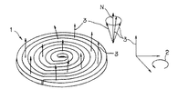
このような超伝導導体(QMG材料)を図1に(a)平面図、(b)側面図を示したように渦巻加工したコイル1にすることによってコイル定数の大きいマグネットが比較的容易にできる。図1では比較的コイル内径が小さい物を一例として示したが、内径の比較的大きな渦巻形状の物についても全く同様に考えることができる。内径が比較的大きな物はコイルの巻き数が減少し発生磁場が減少するが、その一方でより均一で広い磁場空間が得られる利点がある。また、コイルの発生磁界が約20kガウス以下の場合、ボアに鉄芯を入れることにより特性が改善されることは、銅コイルと鉄芯からなる電磁石の例からも明らかである。また、図1にはほぼ同心円状のコイル形状を示したが、楕円状や四角や六角等の形状の物についても全く同様に考えられることは明らかである。
【 0016 】
QMG材料中には大傾角粒界はないが数度の小傾角粒界を伴う結晶方位の揺らぎがある。この揺らぎは結晶の成長方向に依存し、a軸方向に成長した部分は比較的大きな揺らぎの分布を有し、数ミリ角の領域で約±6度、比較的広い領域について調べたものは36度程度との報告がある(Proceedings of 5th U.S.-Japan workshop on high Tc superconductor およびAdvances in Superconductivity II, Springer-Verlag Tokyo 1990)。ここで述べる単結晶状の123相はこのような小傾角粒界を伴っている。
【 0017 】
次に123相の結晶構造は2次元的であり、a-b面で劈開しやすい性質を持っている。したがってa-b面でクラックが発生し易く、現在このようなクラックを完全に無くすことはできていない。このクラックが超伝導電流の流れに悪影響を与えないようにするためには、クラックと電流が平行、すなわち図2のように結晶のc軸が電流2と絶えず垂直になっていることが理想である。しかしながらコイル導体中には、c軸の方位に40度程度の揺らぎがあるため、ある平面内に渦巻状にコイルを巻いたときのその平面の法線Nに対し図2に示すようにc軸の方向3は±20度以内であることが望まれる。
【 0018 】
また、コイルに通電し励磁した場合コイルの内側の導体は、外側の導体に対してより大きな磁界に曝されることになる。またJcは磁場の増加に伴い減少するのが一般的である。したがって、同じ断面積を有するコイルに通電した場合、内側の導体が先に臨界状態に達し、超伝導が壊れコイル自身を損傷することになる。したがって、Jcの磁場特性に合わせ、より内側の導体の断面積がより太くなっていることが望ましい。
【 0019 】
またさらに、磁場を発生している超伝導導体は電磁相互作用により内側から外側へ向かう力(ローレンツ力)を受ける。この力が導体の強度を超えた場合、導体を破壊する。そこでコイルの破壊を防ぐためには、導体同士を機械的に結合し補強することが必要である。そのためには、隣合う導体の隙間を非超伝導物質により埋め、導体同士を固定することが有効である。このとき導体を結合する非超伝導物質は、導体と近い熱膨張係数を有することが望ましい。熱硬化性の樹脂などはこの一例といえる。
【 0020 】
続いて、上記渦巻状コイルを積層して端部間と接続し、それぞれの渦巻状コイルが発生する磁場が互いに強め合うように通電することによって、より強い磁場を発生するマグネットができる。同数の渦巻状コイルを積層するさい、各渦巻状コイルの隙間を小さくしなるべく互いに近づけた方がより高い最高発生磁場が得られる。このためには図3のように渦巻の方向が同じになるよう積層し電流2を内側から外側(または外側から内側)になるように揃え、コイル1間を導体4で接続する方法が考えられる。しかし、図4に(a)積層前、(b)積層後を示したように渦巻コイル1の渦の方向(右巻きまたは左巻き)を交互に逆にして積層し、かつコイル1の内と外の端を交互に接続することによって図3では必要であったコイルをつなぐ導体が不要となり、その厚さの分コイルを密に積層できる。図4(a)において5が接続部分である。
【 0021 】
積層された渦巻コイルの中央部に位置するコイルは、端に位置するコイルに比べ高い磁場に曝されることになる。したがって、同じ断面積を有する積層コイルに通電した場合、中央部のコイルが先に臨界状態に達し、超伝導が壊れコイル自身を損傷することになる。したがって、Jcの磁場特性に合わせ、より中央部のコイルの断面積がより太くなっていることが理想的である。そのためには中央部分の渦巻コイルの層の厚さが端部の渦巻コイルの層の厚さより厚くなっていることが望ましい。
【 0022 】
積層を行った場合、上記のように各渦巻コイルの端部間を接続する必要があるが、QMG材を冷却し通電した状態において、この接続部での発熱を零または極力小さくすることが望ましい。発熱が大きい場合、消費電力や冷媒の消耗が大きくなるだけではなく熱が超伝導導体の超伝導特性を低下させ、さらにはクエンチを引き起こし導体自身を焼損させてしまう。このような要請から接続には、接触抵抗の低い電極を形成し、電気伝導度の大きい金属により接続する必要がある。
【 0023 】
接続部の発熱を完全に零にするには、接続部の電流の経路がすべて超伝導体である必要がある。さらに始端と終端とを単結晶状のQMG材料により接続することによってマグネット全体を単結晶になるようにし、この超伝導体からなる閉回路に電流導入端子および超伝導スイッチを取り付けることによって永久電流モードで動作するマグネットができる。
【 0024 】
本発明の超伝導マグネットの製造方法であるが、コイル形状を得るには、前駆体をコイル形状に加工した後結晶化させる方法(FG法)がある。
【 0025 】
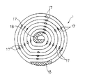
FG法の例を示すと、まずRE、Ba、Cuの酸化物を211相:123相が所定の比になるように混合する。このときPt、Rhを添加すると最終組織の211が微細化する。この混合粉末を金型等により加工成形し前駆体を作製する。この前駆体は圧粉体であるため結晶化したQMG材とは異なりドリルや鋸を用い加工が容易にできる。例えば図5のように、切れ込み7を入れて円柱状の前駆体6を糸鋸によりコイル状に加工することができる。このとき図6の(a)全体図、(b)一部を拡大した平面図に示したように一部切り残した部分8をつくることで半溶融時の変形を少なくすることができる。
【 0026 】
加工された前駆体6は図7のように他のRE組成を有する前駆体9、10、11と重ねられ炉内に配置される。このとき、コイルの隙間に雰囲気が出入りできるようになっていることが結晶成長の観点から望ましい。前駆体9は、コイル状前駆体が多くの切れ込みを有することから、種結晶から成長する結晶が外側のコイルにまで最短距離で届くように、コイル状前駆体6の上部を覆っていることが望ましい。また前駆体9は結晶成長の観点から、コイル状前駆体6のRE組成のTf以上のRE組成からなっていることが望ましい。
【 0027 】
また前駆体10はコイル状前駆体6のRE組成のTfより低いTfのRE組成であり、前駆体11はコイル状前駆体6のRE組成のTfより高いTfのRE組成であることが望ましい。半溶融状態で長時間に保持するためには支持材20との反応を最小限にしかつ種結晶以外からの結晶成長を抑制する必要がある。冷却過程において前駆体11はTfが高いため比較的すばやく結晶化し支持材20との反応を防止する。前駆体10はTfが低いため前駆体11からの結晶成長を防止する。
【 0028 】
Seedingは前駆体6のTf以上、種結晶のTf以下で行われる。このとき種結晶はより大きい方が効率的であり望ましい。前駆体9はコイル状前駆体6と同じRE組成であっても良い。種結晶から成長したQMG結晶は前駆体9を結晶化しさらにコイル状前駆体6を結晶化し、コイル状のQMG結晶ができる。
【 0029 】
コイル状結晶は室温まで冷却された後、ダイヤモンドブレード等により所定の厚さにスライスされる。このとき図6に示したような切り残した部分があるものはスライスするさい機械的ダメージが少ない。切り残した部分を設けない場合、樹脂等により導体間を補強した後スライス加工することが望ましい。
【 0030 】
FG法の利点はコイル加工が成形体(圧粉体)に対して行われるため、高価な加工装置を必要とせず、安価な工具により容易に作製されることにある。また、結晶成長後にコイル形状(バネ形状)を有しているために、機械的歪を緩和し、ひび割れが入りにくいことなどがある。
【 0031 】
上記のようにFG法により作製された渦巻状導体に通電するには、電極を設ける必要がある。電極の接触抵抗はより小さいことが望ましい。電極作製の一例をあげると、所定の位置にAgペーストを塗布した後700℃から超伝導体の分解温度以下の温度域に昇温した後降温する。この降温の際に、酸素富化処理をかね酸化性雰囲気(望ましくは純酸素中)で徐冷することは、プロセスの効率上望ましい。このようにして電極を有する渦巻状のQMG超伝導コイルができる。
【 0032 】
このような渦巻状コイルは取扱いにおける外力やローレンツ力に耐えるため機械的に補強する必要がある。補強には隣合う導体間を結合させることが有効である。補強の一例としては熱硬化樹脂など、硬化時の体積変化の少ない接着剤や熱膨張率がQMG材に近いものが望ましい。また積層されたマグネットに関しても上記の理由から各層間を固定(補強)することが望ましい。
【 0033 】
また、各層を超伝導体で接続するには、各層の結晶方位を合わせる必要がある。結晶方位がほぼ合った状態で互いの接続位置を決定する。コイル接続部分12を図8(a)のように加工し、くぼみ14の部分に超伝導体のTf(Tfc)より低いTf(Tfz)のRE組成の前駆体13を図8(a)のように配置する。これを前駆体13が半溶融状態になりかつコイルが分解しない温度T(Tfc>T>Tfz)にまで加熱する。その後Tfz近傍で徐冷することによって互いに向き合う各層から図8(b)およびこれの部分拡大図(c)のように前駆体13は123相の結晶16が成長し(図では中心部分に結晶成長の残り部分がある)超伝導体15となり、これにより接続された多層コイルができる。
【 0034 】
またさらに1または複数の渦巻状コイルによって形成されたコイルの始端と終端とを結ぶ超伝導体を上記と同様に、導体中のくぼみに前駆体13を配置し熱処理することで、各層の接続およびコイルの始端と終端が超伝導体で接続された、超伝導の閉ループを有するマグネットができる。
【 0035 】
【実施例】
実施例1
市販されている純度99.9%の各試薬Y2O3、BaO2、CuOをY:Ba:Cuの金属元素のモル比が25:35:49(すなわち最終組織の123相:211相のモル比が75:25)になるように混合した。さらにRhを0.2重量%添加した。混合粉は一旦830℃で8時間仮焼され、さらに粉砕された。仮焼粉砕粉は内径85mmの円筒状金型により厚さ約25mmの円盤状に成形された。また上記Y系成形体と同様の方法により厚さ4mmのSm系とDyおよびYb系円盤状成形体を作製した。さらにY系成形体については、等方静水圧プレスにより圧縮加工された。このY系前駆体は図6のような一部がつながった渦巻形状に加工された。この加工はまずドリルにより穴開け加工を行い、しかる後にこの穴に糸鋸の刃を貫通させコイル状に切れ込みを入れることにより行った。
【 0036 】
これらの前駆体は図7に示すようにAl2O3の支持材20の上にSm系、Yb系、Y系、Dy系の順番で下から重ね炉内に配置した。このとき、雰囲気がコイルの内部全体に行き渡るようにYb系前駆体に切れ込みを設けた。これらの前駆体は大気中において1160℃まで8時間で昇温、40分保持された後、1040℃まで1時間で降温し1時間保持した。その間予め作製しておいたNd系の種結晶(QMG結晶)を用いてSeedingを行った。種結晶の方位はc軸が円盤状の前駆体の法線になるように、劈開面を前駆体の上にのせた。その後1015〜975℃まで150時間かけて冷却しY系コイル状QMG結晶の成長を行った。さらに室温まで約15時間かけて冷却した。
【 0037 】
この結晶をダイヤモンドブレードを用い切断(スライス)することによって厚さ約4mmの渦巻コイル状のQMG材を得た。さらにコイルの両端に図10のようにAgペースト18を塗布し880℃に加熱した。880℃で10分保持した後、続いて酸素を炉内に流し650℃から350℃まで50時間かけて冷却し酸素富化処理を行った。室温に冷却した後、エポキシ樹脂17を用いて図10のように補強した。
【 0038 】
このようにして、線の断面積が約3.5mm(幅)×4.0mm(厚さ)の8回巻きのコイルを作製した。そして、このコイルのAg電極に超音波半田を用い銅製の電流端子を接続した。これを液体窒素温度(約77K)に冷却し500Aの電流を流したところ、中心部で約0.90kガウスの磁場を発生することに成功した。
【 0039 】
実施例2
実施例1のY系前駆体のRE組成、前駆体9(図7参照)のRE組成、添加条件、徐冷条件およびコイルの厚さを表1のように変えて同様に実験を行った。この表に示したように各RE組成の超伝導マグネットはクエンチすることなくY系とほぼ同等の磁場を発生した。
【 0040 】
【表1】

実施例3
実施例1で作製したY系渦巻状コイルを図11の(a)積層前、(b)積層後の斜視図に示すように4枚積層した。この時1層目と3層目のコイル1A、1Cは上から見て時計回りに電流が流れたときに中心から外へ流れる向きになっており、また2層目と4層目のコイル1B、1Dは外から中心に向かうように積層した。そして1層目のコイル1A中心部の電極と2層目のコイル1Bの中心部の電極21Aとを低融点の半田(商品名:セラソルザー)を用い超音波半田ごてにより接続した。また同様に2層目のコイル1Cの外側の電極と3層目のコイル1Dの外側の電極21Bとを、3層目の内側の電極と4層目の内側の電極とをそれぞれ接続した。そして1層目と4層目の外側の電極を直流電源の電流リードに接続した。さらに層間をエポキシ樹脂により固定した。
【 0042 】
この4層マグネットを液体窒素中に浸し、マグネットが77Kまで十分冷却された後、500A通電した。層間の電極部で幾分窒素の沸騰が大きくなったものの、マグネットは軸上で図12のグラフのような磁界分布を発生した。
【 0043 】
実施例4
実施例3で作製した4層マグネットを10kガウスの外部磁場中に配置し、液体窒素を投入し77Kに冷却した。そして外部磁場と同じ方向に磁場が発生するように通電した。このとき245A通電した時に超伝導体の一部が焼損した。焼損した部分は第2層目の中間から2巻目であり、超伝導相(123相)は熱により完全に分解していた。
【 0044 】
そこで渦巻の形状を図13のように線の幅を中心部5mm、中間部4.5mm、外周部4mmとし、他の条件を実施例1と同様にして渦巻状コイルを作製した。このときコイルの厚さを4mmと3.5mmの2種類にした。そして1層目と4層目を厚さ3.5mmにし、2層目と3層目を厚さ4mmのものを用いた。実施例5と同様に4つの層を接続し、補強した。
【 0045 】
この4層マグネットを10kガウスの外部磁場中に配置し、液体窒素を投入し77Kに冷却した。そして外部磁場と同じ方向に磁場が発生するように通電した。このとき400A通電することができ中心部において外部磁場と合わせて13.8kガウスを記録した。このことから、中心部でより大きい断面積を有するマグネットが断面積がすべて同じものに比べ優れていることがわかった。
【 0046 】
実施例5
Agペーストによる電極作製工程およびエポキシ樹脂による補強工程を省いた他は実施例1と同じ方法で作製したY系渦巻状コイルを厚さ0.2mmのPt製のスペーサーを配し先の図11(b)に示したものと同様に4枚積層した。この時1層目と3層目のコイル1A、1Cは上から見て時計回りに電流2が流れたときに中心から外へ流れる向きになっており、また2層目と4層目のコイル1B、1Dから外から中心に向かうように積層した。そして1層目の中心部の端と2層目の中心部の端とを図14のように加工し、Yb系前駆体13を配置した。また同様に2層目の外側の端と3層目の外側の端の間、3層目の内側の端と4層目の内側の端の間においても同様の加工およびYb系前駆体の配置を行った。またAgペーストを1および4層目の外側の端に塗布した。
【 0047 】
このように積層されたコイルおよび前駆体は炉内に配置され、大気中で960℃まで8時間で昇温された。この温度で5分保持された後、930℃まで2時間で冷却、さらに870℃まで120時間かけて冷却した。さらに酸素気流中で700℃から350℃まで60時間かけて冷却した後、室温まで冷却した。炉内から慎重に取り出した後、補強のためにエポキシ樹脂を導体間および層間の一部に充填し硬化させた。十分硬化させた後、スペーサーのPt板を抜き取った。また1層目と4層目の外側のAg電極に直流電源の電流リードを低融点半田を用いて接続した。
【 0048 】
この4層マグネットを液体窒素中に浸し、マグネットが77Kまで十分冷却された後、500A通電した。層間の接続部で窒素の沸騰にはほとんど変化がなかった。マグネットは、軸上で図15のような磁界分布を発生した。
【 0049 】
実施例6
Agペーストによる電極作製工程およびエポキシ樹脂による補強工程を省いた他は実施例1と同じ方法で作製したY系渦巻状コイルおよび板状のY系QMG材料を図16のように厚さ0.2mmのPt製のスペーサーを層間に配し4枚積層した。この時1層目と3層目のコイル1A、1Bは上から見て時計回りに電流が流れたとき中心から外へ流れる向きになっており、また2層目と4層目のコイル1B、1Dは外から中心に向かうように積層した。そして1層目の中心部の端と2層目の中心部の端とを先の図14と同様に加工し、Yb系前駆体を配置した。また同様に2層目の外側の端と3層目の外側の端の間、3層目の内側の端と4層目の内側の端の間においても同様の加工およびYb系前駆体の配置を行った。
【 0050 】
また図16および図17に示したように1および4層目の外側の端部と板状QMG材料の両端部においても同様のくぼみ加工14およびYb系の前駆体13を配置した。このとき、板状QMG材料19は1および4層目のQMGコイル材1A、1Dと結晶方位がほぼ一致するように配置した。またAgペースト18を1および4層目の外側の端に塗布した。
【 0051 】
このように積層されたコイルおよび前駆体は炉内に配置され、大気中で960℃まで8時間で昇温された。この温度で5分保持された後、930℃まで2時間で冷却さらに870℃まで120時間かけて冷却した。さらに酸素気流中で700から350℃まで60時間かけて冷却した後、室温まで冷却した。炉内から慎重に取り出した後、補強のためにエポキシ樹脂を導体間および層間の一部に充填し硬化させた。十分硬化させた後、スペーサーのPt板を抜き取った。接続された板状QMG材料に発熱体としてマンガニン線を50回巻き付け、エポキシ樹脂により固定し、超伝導スイッチを作製した。また1層目と4層目の外側のAg電極に直流電源の電流リードを低温半田を用いて接続した。
【 0052 】
この4層マグネットを液体窒素中に浸し、マグネットが77Kまで十分冷却し、マンガニン線に8A通電し一部常伝導状態にした後、マグネットに500A通電した。その後マンガニン線への通電をやめ、マグネットへの通電を100A/minで減らしゼロにした。マグネットは、通電電流をゼロにしてから約30秒後、軸上で図18のような磁界分布を発生した。これにより永久電流モードでの動作が確認された。
【 0053 】
【発明の効果】
以上詳述したごとく本発明は、高品位の酸化物超伝導マグネットを可能にするもので各種分野での応用が可能であり、極めて工業的効果が大きい。具体例としては、実験用各種マグネット、モーター内の励磁用マグネット、加速器用マグネット、核磁気共鳴用マグネット等があげられる。
【図面の簡単な説明】
【図1】 渦巻状コイルの外観を示す(a)平面図および(b)側面図
【図2】 渦巻状コイルの形状と結晶方位との関係を示す図
【図3】 渦巻状コイルの積層方法の例を示す図
【図4】 渦巻状コイルの積層方法の例を示す図で、(a)積層前、(b)積層後を示す
【図5】 前駆体の加工方法の例を示す図
【図6】 前駆体の加工方法の例を示す図で、(a)全体図、(b)一部を拡大した平面図
【図7】 炉内に配置された前駆体を示す図
【図8】 超伝導接合の方法の例を示す図で、(a)コイルの接合部における加工、(b)熱処理後の接合部分、(c)図(b)の一部拡大を示す
【図9】 渦巻コイルのAgペーストおよび補強用樹脂の一例を示す図
【図10】 熱硬化性樹脂で補強された渦巻コイルの例を示す図
【図11】 渦巻状コイルの積層方法の例を示す図で、(a)積層前、(b)積層後を示す
【図12】 本発明の超伝導マグネットの軸上の磁場分布の例を示すグラフ
【図13】 外側の導体の断面積が内側の導体の断面積に比べ小さくなっている渦巻コイルの例を示す図
【図14】 超伝導接合方法の例を示す図
【図15】 本発明の超伝導マグネットの軸上の磁場分布の例を示すグラフ
【図16】 超伝導接続された積層コイルを示す図
【図17】 図16の積層コイルの一部分の超伝導接合方法を示す図
【図18】 本発明の超伝導マグネットの軸上の磁場分布の例を示すグラフ
【符号の説明】
1、1A、1B、1C、1D コイル
2 電流
3 c軸の方位
4 導体
5 接続部分
6、9、10、11、13 前駆体
7 切れ込み
8 切り残した部分
12 接続部分
14 くぼみ
15 超伝導体
16 123相の結晶
17 エポキシ樹脂
18 Agペースト
19 QMG材料
20 支持材
21A、21B 電極
N コイルを形成する面の法線[0001]
[Industrial application fields]
The present invention is substantially REBa 2 Cu 3 O 7-X (0 ≦ x ≦ 0.3) (RE is any one of Y, La, Nd, Sm, Eu, Gd, Dy, Ho, Er, Tm, Yb, and Lu. elements or relate superconducting the magnet preparative method of manufacturing an oxide superconducting material comprising a RE 2 BaCuO 5 Metropolitan combination thereof).
[0002]
[Prior art]
Currently, superconducting magnets are put into practical use mainly by winding Nb-Ti superconducting wire around a coil. In addition, Nb 3 Sn and V 3 Ga-based superconducting materials are made into wires and coiled to be used as high-field superconducting magnets. Since these metal superconducting magnets have a low critical temperature, they must be cooled to a very low temperature with liquid helium. While superconducting magnets have excellent characteristics as magnetic field generators, they have not been widely used due to the necessity of cooling at this extremely low temperature.
[0003]
On the other hand, since the discovery of oxide high temperature superconductors, research and development of magnets using oxide superconducting materials with a critical temperature of 77K or higher that can be cooled and used with liquid nitrogen that is cheap and easy to handle has been actively conducted. Yes. The current mainstream method is to produce a silver sheath tape containing an oriented superconducting material by packing a Bi-based material in an Ag sheath and processing it into a tape shape, and then winding it around a coil. is there. However, such a tape material has not obtained a sufficient critical current density (Jc) at 77K, and has not been put into practical use.
0004
For such a general magnet manufacturing method, after making oxide superconductor into a wire and coiling it, plastic deformation is considered in consideration of difficult workability due to brittleness which is a disadvantage of oxide superconductor It has also been studied to produce a coil-shaped sintered body by heat treatment and use it as a magnet without processing (Japanese Patent Laid-Open No. 63-261808). However, the sintered body (especially Y series) basically includes many grain boundaries, which are weak superconductive bonds and cannot obtain a high critical current density. For this reason, it is difficult for a sintered magnet to generate a high magnetic field while maintaining a superconducting state (Japanese Patent Laid-Open No. 63-261808).
[0005]
At present, the bulk material that can be used as a magnet material having a high Jc even in a high magnetic field at 77K is a material in which RE 2 BaCuO 5 is finely dispersed in single-crystal REBa 2 Cu 3 O 7-X ( Only so-called QMG material). QMG materials can now be made into large single crystal materials by the Pt addition method and Seeding.
[0006]
[Problems to be solved by the invention]
A magnet using QMG material was devised for the first time in Japanese Utility Model Publication No. 4-15811. In this method, a solenoidal coil is formed by cutting a cylindrical QMG superconductor. The magnetic field generated by the magnet is given by the product of the energizing current and the coil constant. The coil constant varies depending on the number of windings and the winding method. When the coil constant is used below the critical density, a large magnetic field can be obtained with a low energization current by increasing the number of windings and the like to increase the coil constant. As can be seen from the figure in Japanese Utility Model Publication No. 4-15811, it is difficult to increase the coil constant by reducing the wire diameter and increasing the number of turns in such a solenoid-shaped magnet from the viewpoint of imparting the shape. . So rather than cut processed solenoid coil cylinder, the development of large new type of the magnet bets preparation of coil function using QMG material has been a problem.
[0007]
[Means for Solving the Problems]
The present invention solves the above-mentioned problem, RE (RE is a rare-earth element including Y and combinations thereof ) , Ba , Cu to produce a molded body from a precursor, and the molded body is spiral After the processing into the coil shape of the above, on the support material, the precursor of the RE composition of Tf higher than the Tf of RE composition of the coiled precursor ( the generation temperature of the REBa 2 Cu 3 O 7-X phase ) , the coiled precursor of RE composition of less than Tf the RE composition of the precursor Tf, stacked in the order of the coiled precursor, further the Tf or more RE composition of RE composition of the coiled precursor precursor form said coil precursor It is placed so as to cover the body, and these are heated to a semi-molten state consisting of the RE 2 BaCuO 5 phase and liquid phase, then the crystal orientation is controlled by the seed crystal, and gradually cooled in an oxidizing atmosphere to form a single crystal after the superconducting material of the coil-shaped molded
[ 0008 ]
Also, a method of manufacturing a superconducting magnet, characterized in that spiral coils produced by the above method are stacked so that the spiral direction (right-handed or left-handed) alternates, and each coil is electrically connected It is. Here, the REBa 2 Cu 3 O 7-X phase, which is a superconducting phase having a Tf lower than the Tf of the coil conductor, is placed between the ends of each spiral coil so that the entire laminated coil becomes a superconductor. It is also characterized by connecting. In addition, the start and end of the coil formed by any of the above methods are connected by a superconducting material having a structure in which RE 2 BaCuO 5 is finely dispersed in a single-crystal REBa 2 Cu 3 O 7-X phase. This is a method of manufacturing a superconducting magnet.
[ 0009 ]
[Action]
The material used for the superconducting magnet of the present invention has a structure in which RE 2 BaCuO 5 is finely dispersed in a single-crystal REBa 2 Cu 3 O 7-X phase. The term “single crystal” as used herein means that not only a perfect single crystal but also a defect having a defect that can be practically used, such as a low-angle grain boundary. RE in REBa 2 Cu 3 O 7-X phase (123 phase) and RE 2 BaCuO 5 phase (211 phase) is from Y, La, Nd, Sm, Eu, Gd, Dy, Ho, Er, Tm, Yb, Lu In the rare earth elements and combinations thereof, the 123 phase containing La and Nd deviates from the 1: 2: 3 stoichiometric composition, and Ba may be partially substituted at the RE site. Also in the 211 phase, La and Nd are somewhat different from Y, Sm, Eu, Gd, Dy, Ho, Er, Tm, Yb, and Lu, and the ratio of metal elements is non-stoichiometric composition or crystal structure Are known to be different.
[ 0010 ]
The 123 phase is a peritectic reaction between the 211 phase and a liquid phase composed of a complex oxide of Ba and Cu.
211 phase + liquid phase (complex oxide of Ba and Cu) → 123 phase. The temperature at which the 123 phase is formed by this peritectic reaction (Tf: 123 phase formation temperature) is substantially related to the ionic radius of the RE element, and Tf decreases as the ionic radius decreases.
[ 0011 ]
The QMG material in which the 211 phase is finely dispersed in the single-crystal 123 phase can be formed because unreacted 211 grains are left in the 123 phase when the 123 phase crystallizes. That is, QMG material is
It can be achieved by the reaction shown by 211 phase + liquid phase (complex oxide of Ba and Cu) → 123 phase + 211 phase.
[ 0012 ]
The fine dispersion of the 211 phase in the QMG material is extremely important from the viewpoint of improving Jc. By adding a small amount of at least one of Pt or Rh, the grain growth of the 211 phase in the semi-molten state (a state consisting of the 211 phase and the liquid phase) is suppressed, and as a result, the 211 phase in the QMG material is refined. . The addition amount is preferably 0.2 to 2.0 wt% for Pt and 0.01 to 0.5 wt% for Rh from the viewpoint of the amount of effect of miniaturization and the material cost. The added Pt or Rh partially dissolves in the 123 phase. In addition, the elements that could not be dissolved form a composite oxide with Ba and Cu and are scattered in the material.
[ 0013 ]
The superconducting magnet obtained by the manufacturing method of the present invention is manufactured by processing a QMG material into a spiral shape (mosquito coil incense shape) wound in a plane and thinning it to produce a magnet with a large coil constant. Alternatively, a magnet having a large coil constant (or number of turns), which was difficult with a solenoid type coil, can be produced by laminating spiral QMG materials.
[ 0014 ]
Specifically, the superconductor constituting the coil needs to have a high critical current density (Jc) even in a magnetic field. In order to satisfy this condition, it is necessary to be a single-crystal 123 phase that does not include a large-angle grain boundary that is weakly superconductive. In order to have higher Jc characteristics, a pinning center is required to stop the movement of magnetic flux. What functions as the pinning center is a finely dispersed 211 phase, and it is desirable that many finely dispersed. As mentioned earlier, Pt and Rh have a function of promoting the refinement of the 211 phase. The 211 phase is also finely dispersed in the 123 phase, which is easy to cleave, so that the superconductor is mechanically strengthened and plays an important role as a bulk material.
[ 0015 ]
By making such a superconducting conductor (QMG material) into a
[ 0016 ]
There is no large-angle grain boundary in the QMG material, but there is fluctuation of crystal orientation with a small-angle grain boundary of several degrees. This fluctuation depends on the crystal growth direction, and the portion grown in the a-axis direction has a relatively large fluctuation distribution, about ± 6 degrees in the area of several millimeters square, and a relatively wide area examined. it has been reported that degree about (Proceedings of 5 th US-Japan workshop on high Tc superconductor and Advances in Superconductivity II, Springer-Verlag Tokyo 1990). The single-crystal 123 phase described here is accompanied by such a low-angle grain boundary.
[ 0017 ]
Next, the 123-phase crystal structure is two-dimensional and has the property of being easily cleaved on the ab plane. Therefore, cracks are likely to occur on the ab surface, and such cracks cannot be completely eliminated at present. In order to prevent this crack from adversely affecting the flow of superconducting current, it is ideal that the crack and current are parallel, that is, the c-axis of the crystal is always perpendicular to current 2 as shown in Fig. 2. is there. However, since there is a fluctuation of about 40 degrees in the direction of the c-axis in the coil conductor, the c-axis as shown in FIG. 2 with respect to the normal N of the plane when the coil is wound in a spiral shape in a certain plane It is desirable that the
[ 0018 ]
In addition, when the coil is energized and excited, the inner conductor of the coil is exposed to a larger magnetic field than the outer conductor. Jc generally decreases as the magnetic field increases. Therefore, when a coil having the same cross-sectional area is energized, the inner conductor first reaches the critical state, and the superconductivity breaks and damages the coil itself. Therefore, it is desirable that the cross-sectional area of the inner conductor is thicker in accordance with the magnetic field characteristics of Jc.
[ 0019 ]
Furthermore, a superconducting conductor generating a magnetic field receives a force (Lorentz force) from the inside toward the outside due to electromagnetic interaction. When this force exceeds the strength of the conductor, the conductor is destroyed. Therefore, in order to prevent destruction of the coil, it is necessary to mechanically connect and reinforce the conductors. For this purpose, it is effective to fix the conductors by filling the gap between adjacent conductors with a non-superconducting material. At this time, it is desirable that the non-superconducting material that binds the conductor has a thermal expansion coefficient close to that of the conductor. A thermosetting resin is an example of this.
[ 0020 ]
Subsequently, a magnet that generates a stronger magnetic field can be obtained by stacking the spiral coils and connecting the ends to each other and energizing the magnetic fields generated by the spiral coils to strengthen each other. When the same number of spiral coils are stacked, a higher maximum generated magnetic field can be obtained when the gaps between the spiral coils are made as close to each other as possible. For this purpose, as shown in FIG. 3, it is possible to stack the coils so that the direction of the spiral is the same, align the current 2 from the inside to the outside (or from the outside to the inside), and connect the
[ 0021 ]
The coil located at the center of the laminated spiral coil is exposed to a higher magnetic field than the coil located at the end. Therefore, when a laminated coil having the same cross-sectional area is energized, the central coil first reaches a critical state, and superconductivity breaks and damages the coil itself. Therefore, it is ideal that the cross-sectional area of the coil at the center is thicker in accordance with the magnetic field characteristics of Jc. For this purpose, it is desirable that the thickness of the spiral coil layer at the central portion is larger than the thickness of the spiral coil layer at the end.
[ 0022 ]
When lamination is performed, it is necessary to connect the ends of each spiral coil as described above. However, when the QMG material is cooled and energized, it is desirable to reduce heat generation at this connection to zero or as much as possible. . When the heat generation is large, not only the power consumption and the consumption of the refrigerant are increased, but the heat deteriorates the superconducting characteristics of the superconducting conductor, and further quenches to burn out the conductor itself. In connection with such a demand, it is necessary to form an electrode with low contact resistance and connect with a metal having high electrical conductivity.
[ 0023 ]
In order to completely eliminate the heat generation at the connection portion, all the current paths of the connection portion must be superconductors. Furthermore, by connecting the start and end with a single-crystal QMG material, the entire magnet is made into a single crystal, and a current introduction terminal and a superconducting switch are attached to the closed circuit made of this superconductor to make a permanent current mode. A magnet that works with
[ 0024 ]
The superconducting magnet manufacturing method of the present invention includes a method (FG method) for obtaining a coil shape by processing the precursor into a coil shape and then crystallizing it.
[ 0025 ]
As an example of the FG method, first, oxides of RE, Ba, and Cu are mixed so that 211 phase: 123 phase has a predetermined ratio. At this time, when Pt and Rh are added, the final structure 211 is refined. The mixed powder is processed and molded with a mold or the like to produce a precursor. Since this precursor is a green compact, it can be easily processed using a drill or saw, unlike the crystallized QMG material. For example, as shown in FIG. 5, the
[ 0026 ]
The processed
[ 0027 ]
Further, it is desirable that the
[ 0028 ]
Seeding is performed at Tf of
[ 0029 ]
The coiled crystal is cooled to room temperature and then sliced to a predetermined thickness with a diamond blade or the like. At this time, as shown in FIG. 6, there is little mechanical damage when slicing when there is an uncut portion. In the case where the uncut portion is not provided, it is desirable to perform slicing after reinforcing conductors with resin or the like.
[ 0030 ]
The advantage of the FG method lies in that coil processing is performed on a compact (green compact), so that an expensive processing device is not required and it is easily manufactured with an inexpensive tool. In addition, since it has a coil shape (spring shape) after crystal growth, it may relieve mechanical strain and prevent cracking.
[ 0031 ]
In order to energize the spiral conductor manufactured by the FG method as described above, it is necessary to provide an electrode. The contact resistance of the electrode is desirably smaller. As an example of electrode production, the Ag paste is applied at a predetermined position, then the temperature is raised from 700 ° C. to a temperature range below the decomposition temperature of the superconductor, and then the temperature is lowered. When the temperature is lowered, it is desirable in terms of process efficiency that the oxygen enrichment treatment is gradually cooled in an oxidizing atmosphere (preferably in pure oxygen). In this manner, a spiral QMG superconducting coil having electrodes can be obtained.
[ 0032 ]
Such a spiral coil needs to be mechanically reinforced in order to withstand external force and Lorentz force during handling. For reinforcement, it is effective to connect adjacent conductors. As an example of reinforcement, an adhesive having a small volume change at the time of curing, such as a thermosetting resin, or a material having a thermal expansion coefficient close to that of a QMG material is desirable. In addition, it is desirable to fix (reinforce) the layers between the laminated magnets for the above reasons.
[ 0033 ]
Moreover, in order to connect each layer with a superconductor, it is necessary to match the crystal orientation of each layer. The mutual connection positions are determined in a state where the crystal orientations are substantially matched. The
[ 0034 ]
Furthermore, the superconductor connecting the starting end and the terminal end of the coil formed by one or more spiral coils is disposed in the recess in the conductor and heat-treated in the same manner as described above, thereby connecting each layer and A magnet having a superconducting closed loop in which the start and end of the coil are connected by a superconductor can be obtained.
[ 0035 ]
【Example】
Example 1
Commercially available reagents of 99.9% purity Y 2 O 3 , BaO 2 , CuO with a Y: Ba: Cu metal element molar ratio of 25:35:49 (i.e., 123 phase of the final structure: 211 phase molar ratio) To 75:25). Further, 0.2% by weight of Rh was added. The mixed powder was temporarily calcined at 830 ° C. for 8 hours and further pulverized. The calcined pulverized powder was formed into a disk shape having a thickness of about 25 mm by a cylindrical mold having an inner diameter of 85 mm. In addition, Sm-based and Dy- and Yb-based disk-shaped molded bodies having a thickness of 4 mm were produced in the same manner as the Y-based molded bodies. Further, the Y-based molded body was compressed by an isotropic hydrostatic press. This Y-based precursor was processed into a spiral shape with a part connected as shown in FIG. This processing was performed by first drilling with a drill, and then inserting a blade of a saw blade into the hole to make a cut in a coil shape.
[ 0036 ]
As shown in FIG. 7, these precursors were placed on the Al 2 O 3 support 20 in the stacking furnace from the bottom in the order of Sm, Yb, Y, and Dy. At this time, cuts were made in the Yb-based precursor so that the atmosphere would spread throughout the interior of the coil. These precursors were heated in air to 1160 ° C. in 8 hours and held for 40 minutes, and then lowered to 1040 ° C. in 1 hour and held for 1 hour. Meanwhile, seeding was performed using a Nd-based seed crystal (QMG crystal) prepared in advance. The cleaved surface was placed on the precursor so that the orientation of the seed crystal was normal to the disc-shaped precursor. Thereafter, it was cooled to 1015 to 975 ° C. over 150 hours to grow a Y-based coiled QMG crystal. Furthermore, it cooled to room temperature over about 15 hours.
[ 0037 ]
This crystal was cut (sliced) with a diamond blade to obtain a spiral coiled QMG material having a thickness of about 4 mm. Further,
[ 0038 ]
In this manner, an 8-turn coil having a wire cross-sectional area of about 3.5 mm (width) × 4.0 mm (thickness) was produced. A copper current terminal was connected to the Ag electrode of the coil using ultrasonic solder. When this was cooled to liquid nitrogen temperature (about 77 K) and a current of 500 A was applied, a magnetic field of about 0.90 k Gauss was successfully generated in the center.
[ 0039 ]
Example 2
Experiments were similarly performed by changing the RE composition of the Y-based precursor of Example 1, the RE composition of the precursor 9 (see FIG. 7), the addition conditions, the slow cooling conditions, and the coil thickness as shown in Table 1 . As shown in this table, superconducting magnets with each RE composition generated a magnetic field almost equivalent to that of the Y system without quenching.
[ 0040 ]
【table 1】
Example 3
Four Y-series spiral coils produced in Example 1 were laminated as shown in the perspective view of FIG. 11 (a) before lamination and (b) after lamination. At this time, the
[ 0042 ]
This four-layer magnet was immersed in liquid nitrogen, and after the magnet was sufficiently cooled to 77K, 500 A was energized. Although the nitrogen boiling somewhat increased between the electrode portions between the layers, the magnet generated a magnetic field distribution on the axis as shown in the graph of FIG.
[ 0043 ]
Example 4
The four-layer magnet produced in Example 3 was placed in an external magnetic field of 10 k gauss, and liquid nitrogen was introduced and cooled to 77K. And it supplied with electricity so that a magnetic field might be generated in the same direction as an external magnetic field. At this time, a part of the superconductor burned out when 245 A was energized. The burned portion was the second volume from the middle of the second layer, and the superconducting phase (123 phase) was completely decomposed by heat.
[ 0044 ]
Therefore, as shown in FIG. 13, a spiral coil was manufactured in the same manner as in Example 1 except that the width of the line was 5 mm in the center, 4.5 mm in the middle, and 4 mm in the outer periphery. At this time, the thickness of the coil was made into two types of 4mm and 3.5mm. The first and fourth layers were 3.5 mm thick, and the second and third layers were 4 mm thick. As in Example 5, four layers were connected and reinforced.
[ 0045 ]
This four-layer magnet was placed in an external magnetic field of 10k gauss, and liquid nitrogen was added to cool to 77K. And it supplied with electricity so that a magnetic field might be generated in the same direction as an external magnetic field. At this time, it was possible to energize 400A and recorded 13.8k Gauss together with the external magnetic field in the center. From this, it was found that magnets having a larger cross-sectional area at the center are superior to those having the same cross-sectional area.
[ 0046 ]
Example 5
Except for the electrode preparation process using Ag paste and the reinforcement process using epoxy resin, a Y-type spiral coil manufactured by the same method as in Example 1 was arranged with a Pt spacer with a thickness of 0.2 mm as shown in FIG. 4 sheets were laminated in the same manner as shown in (1). At this time, the
[ 0047 ]
The coil and precursor thus laminated were placed in a furnace and heated to 960 ° C. in the atmosphere for 8 hours. After being kept at this temperature for 5 minutes, it was cooled to 930 ° C. in 2 hours and further cooled to 870 ° C. over 120 hours. Further, the mixture was cooled from 700 ° C. to 350 ° C. over 60 hours in an oxygen stream, and then cooled to room temperature. After careful removal from the furnace, epoxy resin was filled between the conductors and part of the layers for curing to be cured. After sufficiently curing, the spacer Pt plate was pulled out. The current leads of the DC power source were connected to the outer Ag electrodes of the first and fourth layers using low melting point solder.
[ 0048 ]
This four-layer magnet was immersed in liquid nitrogen, and after the magnet was sufficiently cooled to 77K, 500 A was energized. There was almost no change in the boiling of nitrogen at the connection between the layers. The magnet generated a magnetic field distribution as shown in Fig. 15 on the axis.
[ 0049 ]
Example 6
Except for the electrode preparation process using Ag paste and the reinforcement process using epoxy resin, the Y-type spiral coil and the plate-like Y-type QMG material produced by the same method as in Example 1 were 0.2 mm thick as shown in Fig. 16. Four Pt spacers were placed between the layers and stacked. At this time, the
[ 0050 ]
Further, as shown in FIG. 16 and FIG. 17, the
[ 0051 ]
The coil and precursor thus laminated were placed in a furnace and heated to 960 ° C. in the atmosphere for 8 hours. After being kept at this temperature for 5 minutes, it was cooled to 930 ° C. in 2 hours and further cooled to 870 ° C. over 120 hours. Further, the mixture was cooled from 700 to 350 ° C. in an oxygen stream over 60 hours, and then cooled to room temperature. After careful removal from the furnace, epoxy resin was filled between the conductors and part of the layers for curing to be cured. After sufficiently curing, the spacer Pt plate was pulled out. A manganin wire was wound 50 times around the connected plate-like QMG material as a heating element and fixed with an epoxy resin to produce a superconducting switch. The current leads of the DC power source were connected to the outer Ag electrodes of the first and fourth layers using low temperature solder.
[ 0052 ]
This four-layer magnet was immersed in liquid nitrogen, the magnet was sufficiently cooled to 77K, 8A current was applied to the manganin wire to make it partially normal, and then 500A current was supplied to the magnet. After that, the power supply to the manganin wire was stopped and the power supply to the magnet was reduced to 100A / min to zero. The magnet generated a magnetic field distribution as shown in Fig. 18 about 30 seconds after the energization current was zero. This confirmed the operation in the permanent current mode.
[ 0053 ]
【The invention's effect】
As described above in detail, the present invention enables a high-quality oxide superconducting magnet and can be applied in various fields, and has a great industrial effect. Specific examples include various experimental magnets, excitation magnets in motors, accelerator magnets, and nuclear magnetic resonance magnets.
[Brief description of the drawings]
[Fig. 1] (a) Plan view and (b) Side view showing appearance of spiral coil [Fig. 2] Diagram showing relationship between spiral coil shape and crystal orientation [Fig. 3] Method of stacking spiral coils Fig. 4 is a diagram showing an example of a spiral coil lamination method, (a) before lamination, (b) after lamination [Fig. 5] An example of precursor processing method [ 6 is a diagram showing an example of a processing method of a precursor, (a) general view, (b) a partially enlarged plan view [FIG. 7] a diagram showing a precursor placed in a furnace [FIG. 8] FIG. 9 is a diagram showing an example of a superconducting joining method, showing (a) processing at the joint of the coil, (b) the joint after the heat treatment, and (c) a partial enlargement of FIG. 9 (b). FIG. 10 is a diagram showing an example of a spiral coil reinforced with a thermosetting resin. FIG. 11 is a diagram showing an example of a spiral coil lamination method. ) Before lamination, (b) After lamination [Figure 12] Book A graph showing an example of the magnetic field distribution on the axis of a bright superconducting magnet [Fig. 13] A diagram showing an example of a spiral coil in which the cross-sectional area of the outer conductor is smaller than the cross-sectional area of the inner conductor [Fig. 14] FIG. 15 is a graph showing an example of the magnetic field distribution on the axis of the superconducting magnet of the present invention. FIG. 16 is a diagram showing a superconductingly connected laminated coil. The figure which shows the superconducting joining method of a part of laminated coil of FIG. 18 [FIG. 18] The graph which shows the example of the magnetic field distribution on the axis | shaft of the superconducting magnet of this invention
1, 1A, 1B, 1C, 1D coil
2 Current
3 c-axis orientation
4 conductor
5 Connection part
6, 9, 10, 11, 13 precursor
7 notches
8 Uncut part
12 Connection part
14 Recess
15 Superconductor
16 123 phase crystals
17 Epoxy resin
18 Ag paste
19 QMG material
20 Support material
21A, 21B electrode
N Normal of the surface forming the coil
Claims (5)
Priority Applications (3)
| Application Number | Priority Date | Filing Date | Title |
|---|---|---|---|
| JP5828394A JP3794591B2 (en) | 1994-03-04 | 1994-03-04 | Manufacturing method of superconducting magnet |
| CNB951903039A CN1152396C (en) | 1994-03-04 | 1995-03-03 | Superconducting magnet and production method thereof |
| PCT/JP1995/000351 WO1995024047A1 (en) | 1994-03-04 | 1995-03-03 | Superconducting magnet and production method thereof |
Applications Claiming Priority (1)
| Application Number | Priority Date | Filing Date | Title |
|---|---|---|---|
| JP5828394A JP3794591B2 (en) | 1994-03-04 | 1994-03-04 | Manufacturing method of superconducting magnet |
Related Child Applications (1)
| Application Number | Title | Priority Date | Filing Date |
|---|---|---|---|
| JP2006044723A Division JP2006222435A (en) | 2006-02-22 | 2006-02-22 | Superconducting magnet |
Publications (2)
| Publication Number | Publication Date |
|---|---|
| JPH07245211A JPH07245211A (en) | 1995-09-19 |
| JP3794591B2 true JP3794591B2 (en) | 2006-07-05 |
Family
ID=13079870
Family Applications (1)
| Application Number | Title | Priority Date | Filing Date |
|---|---|---|---|
| JP5828394A Expired - Lifetime JP3794591B2 (en) | 1994-03-04 | 1994-03-04 | Manufacturing method of superconducting magnet |
Country Status (3)
| Country | Link |
|---|---|
| JP (1) | JP3794591B2 (en) |
| CN (1) | CN1152396C (en) |
| WO (1) | WO1995024047A1 (en) |
Families Citing this family (19)
| Publication number | Priority date | Publication date | Assignee | Title |
|---|---|---|---|---|
| CN103474168B (en) * | 2012-06-07 | 2016-08-03 | 清华大学 | superconducting wire |
| RU2254633C1 (en) * | 2003-10-27 | 2005-06-20 | Российский научный центр "Курчатовский институт" | Method for manufacturing superconductor windings (alternatives) |
| JP4603331B2 (en) * | 2003-12-02 | 2010-12-22 | 新日本製鐵株式会社 | Oxide superconductor processing method, oxide superconducting energization element and superconducting magnet |
| JP4799979B2 (en) * | 2005-04-28 | 2011-10-26 | 新日本製鐵株式会社 | Oxide superconductor coil, oxide superconductor coil manufacturing method, oxide superconductor coil excitation method, oxide superconductor coil cooling method, and magnet system |
| CN101213468B (en) * | 2005-06-28 | 2012-06-27 | 皇家飞利浦电子股份有限公司 | Ferromagnetic shield for magnetic resonance imaging |
| JP4903729B2 (en) * | 2008-01-11 | 2012-03-28 | 新日本製鐵株式会社 | Oxide superconducting magnet, manufacturing method thereof, and cooling method |
| WO2011071071A1 (en) * | 2009-12-08 | 2011-06-16 | 新日本製鐵株式会社 | Oxide superconducting bulk magnet member |
| JP4865081B2 (en) * | 2009-12-08 | 2012-02-01 | 新日本製鐵株式会社 | Oxide superconducting bulk magnet member |
| JP4719308B1 (en) * | 2009-12-08 | 2011-07-06 | 新日本製鐵株式会社 | Oxide superconducting bulk magnet member |
| JP6373285B2 (en) | 2014-02-05 | 2018-08-15 | 古河電気工業株式会社 | Superconducting coil |
| CN104779841B (en) * | 2015-04-09 | 2017-03-08 | 浙江东晶电子股份有限公司 | A kind of method that utilization spherical coil supporting structure carries out superconducting rotor suspension |
| CN106298150B (en) * | 2016-09-13 | 2018-07-31 | 华北电力大学 | A kind of superconducting magnet and preparation method based on ReBCO spiral coating conductor pieces |
| CN106298149B (en) * | 2016-09-13 | 2018-01-23 | 华北电力大学 | A kind of conduction cooling superconducting magnet and preparation based on ReBCO spiral coating conductor pieces |
| CN106298151B (en) * | 2016-10-10 | 2018-06-22 | 华北电力大学 | A kind of class bit superconducting magnet based on ReBCO coatings |
| CN106449006B (en) * | 2016-10-10 | 2018-06-22 | 华北电力大学 | A kind of conduction cooling magnet based on ReBCO coating conductor pieces |
| JP7032392B2 (en) * | 2017-05-15 | 2022-03-08 | 国立研究開発法人理化学研究所 | Superconducting magnet |
| CN108470617A (en) * | 2018-05-30 | 2018-08-31 | 上海交通大学 | High-temperature superconductor closing coil constant current switch structure and its working method |
| WO2019229947A1 (en) * | 2018-05-31 | 2019-12-05 | 三菱電機株式会社 | Superconducting magnet |
| JP7290006B2 (en) * | 2019-01-10 | 2023-06-13 | 国立大学法人山梨大学 | High frequency superconducting laminate |
Family Cites Families (8)
| Publication number | Priority date | Publication date | Assignee | Title |
|---|---|---|---|---|
| JPH0777168B2 (en) * | 1987-03-31 | 1995-08-16 | 住友電気工業株式会社 | Superconducting coil |
| JPH0713924B2 (en) * | 1987-04-24 | 1995-02-15 | 住友電気工業株式会社 | Superconducting magnet |
| JPH0782939B2 (en) * | 1989-01-20 | 1995-09-06 | 新日本製鐵株式会社 | Magnet using oxide superconductor and method for manufacturing the same |
| JP3018534B2 (en) * | 1991-03-20 | 2000-03-13 | 住友電気工業株式会社 | High temperature superconducting coil |
| JPH0582330A (en) * | 1991-09-20 | 1993-04-02 | Furukawa Electric Co Ltd:The | Manufacture of oxide series superconductor coil |
| JPH0812820B2 (en) * | 1992-04-02 | 1996-02-07 | 新日本製鐵株式会社 | Superconducting magnet |
| JPH05301716A (en) * | 1992-04-28 | 1993-11-16 | Nippon Steel Corp | Oxide superconductor produced by utilizing solid-phase diffusion and production process |
| JPH05315127A (en) * | 1992-05-06 | 1993-11-26 | Sumitomo Heavy Ind Ltd | Manufacture of superconducting coil |
-
1994
- 1994-03-04 JP JP5828394A patent/JP3794591B2/en not_active Expired - Lifetime
-
1995
- 1995-03-03 CN CNB951903039A patent/CN1152396C/en not_active Expired - Lifetime
- 1995-03-03 WO PCT/JP1995/000351 patent/WO1995024047A1/en active Application Filing
Also Published As
| Publication number | Publication date |
|---|---|
| WO1995024047A1 (en) | 1995-09-08 |
| JPH07245211A (en) | 1995-09-19 |
| CN1127050A (en) | 1996-07-17 |
| CN1152396C (en) | 2004-06-02 |
Similar Documents
| Publication | Publication Date | Title |
|---|---|---|
| JP3794591B2 (en) | Manufacturing method of superconducting magnet | |
| CA2622384C (en) | High temperature superconducting wires and coils | |
| US6925316B2 (en) | Method of forming superconducting magnets using stacked LTS/HTS coated conductor | |
| JP5568361B2 (en) | Superconducting wire electrode joint structure, superconducting wire, and superconducting coil | |
| JP4653555B2 (en) | Oxide superconducting magnet material and oxide superconducting magnet system | |
| WO2012056698A1 (en) | Oxide superconductivity wire material and method of manufacturing thereof | |
| JP4799979B2 (en) | Oxide superconductor coil, oxide superconductor coil manufacturing method, oxide superconductor coil excitation method, oxide superconductor coil cooling method, and magnet system | |
| JP4362009B2 (en) | Method of manufacturing a coil from high temperature superconducting material and low AC loss high temperature superconducting coil | |
| Okada | Development of Bi-2212/Ag round-shaped wire and magnet application | |
| EP0292436A2 (en) | High current conductors and high field magnets using anisotropic superconductors | |
| JP4719308B1 (en) | Oxide superconducting bulk magnet member | |
| JP5675232B2 (en) | Superconducting current lead | |
| JP2006222435A (en) | Superconducting magnet | |
| JP5405069B2 (en) | Tape-shaped oxide superconductor and substrate used therefor | |
| JP2012064323A (en) | Superconductive current lead | |
| JP4634908B2 (en) | High temperature superconducting coil | |
| JP4414617B2 (en) | Low resistance conductor, its manufacturing method, current lead, power supply cable, coil, magnetic field generator, transformer and AC power supply | |
| JP4011131B2 (en) | Tape-shaped oxide superconducting wire, superconducting magnet and current lead using the same | |
| US20150357091A1 (en) | Re123-based superconducting wire and method of manufacturing the same | |
| JP4603331B2 (en) | Oxide superconductor processing method, oxide superconducting energization element and superconducting magnet | |
| WO2013015328A1 (en) | Base material for superconducting thin film, superconducting thin film, and method for manufacturing superconducting thin film | |
| JP4903729B2 (en) | Oxide superconducting magnet, manufacturing method thereof, and cooling method | |
| JPH0812820B2 (en) | Superconducting magnet | |
| JPH05135935A (en) | Oxide superconductive coil | |
| JPH0950718A (en) | Rare earth oxide superconducting material and its manufacture |
Legal Events
| Date | Code | Title | Description |
|---|---|---|---|
| A02 | Decision of refusal |
Free format text: JAPANESE INTERMEDIATE CODE: A02 Effective date: 20030812 |
|
| A521 | Written amendment |
Free format text: JAPANESE INTERMEDIATE CODE: A523 Effective date: 20060222 |
|
| A61 | First payment of annual fees (during grant procedure) |
Free format text: JAPANESE INTERMEDIATE CODE: A61 Effective date: 20060407 |
|
| FPAY | Renewal fee payment (event date is renewal date of database) |
Free format text: PAYMENT UNTIL: 20090421 Year of fee payment: 3 |
|
| FPAY | Renewal fee payment (event date is renewal date of database) |
Free format text: PAYMENT UNTIL: 20100421 Year of fee payment: 4 |
|
| FPAY | Renewal fee payment (event date is renewal date of database) |
Free format text: PAYMENT UNTIL: 20110421 Year of fee payment: 5 |
|
| FPAY | Renewal fee payment (event date is renewal date of database) |
Free format text: PAYMENT UNTIL: 20120421 Year of fee payment: 6 |
|
| FPAY | Renewal fee payment (event date is renewal date of database) |
Free format text: PAYMENT UNTIL: 20130421 Year of fee payment: 7 |
|
| FPAY | Renewal fee payment (event date is renewal date of database) |
Free format text: PAYMENT UNTIL: 20130421 Year of fee payment: 7 |
|
| S531 | Written request for registration of change of domicile |
Free format text: JAPANESE INTERMEDIATE CODE: R313531 |
|
| R350 | Written notification of registration of transfer |
Free format text: JAPANESE INTERMEDIATE CODE: R350 |
|
| FPAY | Renewal fee payment (event date is renewal date of database) |
Free format text: PAYMENT UNTIL: 20130421 Year of fee payment: 7 |
|
| S533 | Written request for registration of change of name |
Free format text: JAPANESE INTERMEDIATE CODE: R313533 |
|
| FPAY | Renewal fee payment (event date is renewal date of database) |
Free format text: PAYMENT UNTIL: 20130421 Year of fee payment: 7 |
|
| R350 | Written notification of registration of transfer |
Free format text: JAPANESE INTERMEDIATE CODE: R350 |
|
| FPAY | Renewal fee payment (event date is renewal date of database) |
Free format text: PAYMENT UNTIL: 20140421 Year of fee payment: 8 |
|
| EXPY | Cancellation because of completion of term |