JP3772668B2 - Oscillation circuit using phase-locked loop - Google Patents
Oscillation circuit using phase-locked loop Download PDFInfo
- Publication number
- JP3772668B2 JP3772668B2 JP2000361557A JP2000361557A JP3772668B2 JP 3772668 B2 JP3772668 B2 JP 3772668B2 JP 2000361557 A JP2000361557 A JP 2000361557A JP 2000361557 A JP2000361557 A JP 2000361557A JP 3772668 B2 JP3772668 B2 JP 3772668B2
- Authority
- JP
- Japan
- Prior art keywords
- clock signal
- controlled oscillator
- voltage
- output
- voltage controlled
- Prior art date
- Legal status (The legal status is an assumption and is not a legal conclusion. Google has not performed a legal analysis and makes no representation as to the accuracy of the status listed.)
- Expired - Fee Related
Links
- 230000010355 oscillation Effects 0.000 title claims description 54
- 230000000630 rising effect Effects 0.000 claims description 23
- 238000000034 method Methods 0.000 claims description 4
- 230000010363 phase shift Effects 0.000 claims description 2
- 238000010586 diagram Methods 0.000 description 12
- 230000007704 transition Effects 0.000 description 7
- 230000007423 decrease Effects 0.000 description 5
- 230000003111 delayed effect Effects 0.000 description 5
- 238000006243 chemical reaction Methods 0.000 description 4
- 239000003990 capacitor Substances 0.000 description 3
- 230000000694 effects Effects 0.000 description 3
- 230000002238 attenuated effect Effects 0.000 description 2
- 230000000737 periodic effect Effects 0.000 description 2
- 239000000919 ceramic Substances 0.000 description 1
- 239000013078 crystal Substances 0.000 description 1
- 230000001360 synchronised effect Effects 0.000 description 1
Images
Landscapes
- Stabilization Of Oscillater, Synchronisation, Frequency Synthesizers (AREA)
Description
【0001】
【発明の属する技術分野】
本発明は、位相同期ループを用いた発振回路に関わり、特に出力クロック信号に発生するジッタを低減する手法を提供するものである。
【0002】
【従来の技術】
位相同期ループを用いた発振回路は広く一般的に用いられている。その典型的な回路構成は図9のようなものである。位相周波数比較器1の一方の入力端子には、周波数がfrである入力クロック信号S1が入力される。位相周波数比較器1の出力する誤差信号S2は、ループフィルタ2に入力される。ループフィルタ2の出力電圧信号S3は、電圧制御発振器3に入力される。電圧制御発振器3の出力クロック信号S4は、発振回路の出力として外部に取り出されるとともに分周器5に入力される。分周器5は信号S4をN分周して、周波数fo/Nの帰還クロック信号S6を生成する。帰還クロック信号S6は、位相周波数比較器1の他方の入力端子に帰還される。
【0003】
ここで、帰還クロック信号S6の周波数fo/Nが入力クロック信号S1の周波数frよりも低いと、位相周波数比較器1は、帰還クロック信号S6の位相が遅れている期間だけ正の誤差信号S2を出力する。ループフィルタ2は低域通過特性を持つよう構成されており、誤差信号S2は積分され、電圧制御発振器3の入力電圧信号S3は上昇する。S3が上昇すると、それに応じて電圧制御発振器3は発振周波数を変化させ、出力クロック信号S4の周波数foも上昇する。逆に、帰還クロック信号S6の周波数fo/Nが入力クロック信号S1の周波数frよりも高ければ、位相周波数比較器1は、帰還クロック信号S6の位相が進んでいる期間だけ負の誤差信号S2を出力する。ループフィルタ2はこの誤差信号S2を積分するので、電圧制御発振器3の入力電圧信号S3は低下し、出力クロック信号S4の周波数foも低下する。このような負帰還作用によって、定常状態においては、周波数fo/Nはfrと完全に等しくなる。すなわち、入力クロック信号S1の周波数frをN逓倍した周波数foが、出力クロック信号S4として得られる。
【0004】
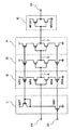
電圧制御発振器3の具体的な構成としては、大別して、電気的あるいは機械的な共振現象を利用したものと、K個(通常Kは奇数)のインバータ回路を環状に接続してなるリングオシレータ形式のものとがある。
【0005】
図10は、電気的な共振現象を利用した電圧制御発振器3の一構成例である。I11は発振部であり、インダクタL1,L2のインダクタンスと、pn接合ダイオードD1,D2の端子間容量の総和とで決まる共振周波数に等しい発振信号が得られる。入力電圧信号S3を変化させると、その電圧値に応じてpn接合ダイオードD1,D2の端子間容量が変化するため、それに連れて共振周波数が変化し、発振信号の周波数を可変することができる。I11の発振出力は差動信号A1,B1として得られ、後段の差動−シングル変換回路I12によってシングルエンド信号C1に変換された上、インバータ回路I13によって波形整形されて出力クロック信号S4が生成される。次に、このような電気的な共振現象を利用した電圧制御発振器を図9の発振回路に適用したときの、定常状態におけるタイミングチャートを図11に示す。発振部I11の差動信号A1,B1と、差動−シングル変換回路I12の出力信号C1、および電圧制御発振器3の出力クロック信号S4は、いずれも周期Tの間隔で状態遷移を繰り返し、その状態遷移の発生はほぼ同一時点である。分周器5は電圧制御発振器3の出力信号S4をN分周(本例ではN=4)して、帰還クロック信号S6を生成する。帰還クロック信号S6は、位相同期ループによって、入力クロック信号S1にロックされるので、両者は同位相となる。なお、ここでは理解を容易にするために、すべての波形を理想的な方形波として描画しており、必ずしも現実を忠実に表しているものではないことを注意しておく。また、インダクタL1,L2およびpn接合ダイオードD1,D2に代えて、水晶振動子、セラミック発振子、SAW共振子などの機械的な共振器を利用して同種の電圧制御発振器を構成することも可能である。この場合、基本的な動作は電気的な共振現象を利用したものと本質的には同じであるので、ここでは詳細な説明を省略する。
【0006】
一方、図12は、K個のインバータ回路を環状に接続してなるリングオシレータ形式の電圧制御発振器3の一構成例である。ここでは、K=3の例を示している。I22,I23,I24は、それぞれがインバータ回路を構成している。I22の出力A2はI23に入力され、I23の出力B2はI24に入力され、I24の出力C2はI22に入力されて環状接続をなし、リングオシレータが形成される。I24の出力C2は、インバータ回路I25で波形整形されて出力クロック信号S4となる。いま、インバータ回路I22,I23,I24の各々の伝播遅延をτとすると、発振信号の周波数foは1/2Kτとなる。ここで、伝播遅延τは、各インバータ回路の出力電流と入力容量とで決定される。入力電圧信号S3を変化させると、電圧−電流変換回路I21によって入力電圧信号S3に応じた電流が生成され、その電流値に連動して各インバータ回路の出力電流値が変化するので、発振信号の周波数を可変することができる。次に、このようなK個のインバータ回路を環状に接続してなるリングオシレータ形式の電圧制御発振器を図9の発振回路に適用したときの、定常状態におけるタイミングチャートを図13に示す。同図から明らかなように、信号A2が反転してτだけ遅延したものが信号B2、信号B2が反転してτだけ遅延したものが信号C2、信号C2が反転してτだけ遅延したものが信号A2という関係にある。すなわち、環状接続を一巡することによる伝播遅延の総和Kτを半周期とする発振動作が得られるので、前述したように、発振周波数foは1/2Kτとなる。本方式の電圧制御発振器においては、τ時間毎にいずれか一つのインバータ回路が状態遷移を行うのが特徴である。ここで、発振周期をTとすると、τ=T/2Kである。以降の動作は、先に説明した図11と同様であり、分周器5が電圧制御発振器3の出力信号S4をN分周(本例ではN=4)して、帰還クロック信号S6を生成する。帰還クロック信号S6は、位相同期ループによって、入力クロック信号S1にロックされるので、両者は同位相となる。なお、ここでも理解を容易にするために、すべての波形を理想的な方形波として描画したが、先と同様に必ずしも現実を忠実に表しているものではないことを注意しておく。
【0007】
【発明が解決しようとする課題】
しかしながら、このような従来の構成においては、位相周波数比較器1や分周器5を構成する論理回路の状態遷移によって、電源電圧や電圧制御発振器3の入力電圧信号S3にスパイク状の変動が発生する。この変動は電圧制御発振器3の動作を不安定なものとし、その出力クロック信号S4には入力クロック信号S1と同期した周期的なノイズが重畳する。この結果、出力クロック信号S4にジッタと呼ばれるエッジの揺らぎが発生する。例えば、図11の最下段に示したノイズ波形は、発振回路の電源電圧に重畳するノイズを例示しているが、中でも帰還クロック信号S6の状態遷移に一致して現れるスパイク状のノイズが顕著である。これは、位相周波数比較器1や分周器5の動作に起因するノイズである。このスパイク状のノイズの発生点は、電圧制御発振器3の内部信号A1,B1,C1の立ち上がり、もしくは立ち下がりエッジと一致している。すなわち、これら信号のエッジはノイズによって揺らぎを生じてしまい、周期的なジッタとなる。同様の現象は、図13にも示されている。この場合、スパイク状のノイズは電圧制御発振器3の内部信号C2の立ち下がりエッジと一致している。これにより、信号C2の立ち下がりエッジが揺らぎを生じる。さらには、一定の位相関係を保って連鎖的に動作する信号A2,B2にも影響が波及し、電圧制御発振器3全体が不安定となって、大きなジッタが発生してしまう。なお、このようなスパイク状のノイズは、電源電圧だけではなく、電圧制御発振器3の入力電圧信号S3にも出現する。
【0008】
本発明は、このような従来技術の欠点を解消するためになされたものであり、前述したスパイク状のノイズが発生しても電圧制御発振器3の動作を極力安定に保ち、結果としてジッタの発生量が極めて少ない発振回路を提供することを目的とする。
【0009】
【課題を解決するための手段】
本発明の発振回路は、従来の回路構成に加えて、電圧制御発振器3の出力と分周器5の入力との間に遅延回路を挿入することによって、上述の課題を解決した。遅延回路に設定される遅延量は、電圧制御発振器の構成によって異なり、帰還クロック信号S6の立ち上がりエッジおよび立ち下がりエッジが、電圧制御発振器3の内部に存在するすべてのクロック信号の立ち上がりエッジ、立ち下がりエッジから最も乖離した位置となるように設定される。すなわち、電圧制御発振器3が電気的あるいは機械的な共振現象を利用したものである場合は、帰還クロック信号S6の立ち上がりエッジ、立ち下がりエッジのいずれかと、電圧制御発振器3の出力クロック信号S4の立ち上がりエッジまたは立ち下がりエッジとの時間差が、電圧制御発振器3の出力クロック信号S4の発振周期に対して1/4またはその奇数倍に概ね等しく設定される。一方、電圧制御発振器3がK個のインバータ回路を環状に接続してなるリングオシレータ形式のものである場合は、帰還クロック信号S6の立ち上がりエッジ、立ち下がりエッジのいずれかと、電圧制御発振器3の出力クロック信号S4の立ち上がりエッジまたは立ち下がりエッジとの時間差が、電圧制御発振器3の出力クロック信号S4の発振周期に対し1/(4K)またはその奇数倍に概ね等しく設定される。このように構成することにより、位相周波数比較器1や分周器5を構成する論理回路の状態遷移によって、電源電圧や電圧制御発振器3の入力電圧信号S3にスパイク状のノイズが発生したとしても、そのスパイクの発生は、電圧制御発振器3の内部に存在するいずれの発振波形の立ち上がり、または立ち下がりエッジからも最も乖離した時点となるため、電圧制御発振器3の動作は極力安定に保たれる。この結果、出力クロック信号S4に発生するジッタは極めて少なくなる。
【0010】
さらに、遅延手段の遅延量が、電圧制御発振器3の入力電圧信号S3によって可変されるよう構成すれば、例え入力クロック信号S1の周波数frが変化したり、分周器5の分周数Nが切り替えられたりして、電圧制御発振器3の出力クロック信号S4の周波数foが変化した場合であっても、当該遅延量が所望の値を維持するように設定することが可能である。また、電圧制御発振器3が、電気的あるいは機械的な共振現象を利用したものであれば、遅延手段を90度移相器で置き換えることによっても、同様の機能を持たせることができる。
【0011】
【発明の実施の形態】
以下、本発明による発振回路の実施の形態を、請求項1ないし4にそれぞれ対応させて、第一ないし第四の実施形態として詳細に説明する。
【0012】
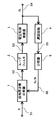
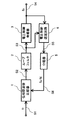
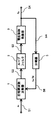
(第一の実施形態)
図1は、本発明の第一および第二の実施形態に共通な発振回路の構成例を示すブロック図である。位相周波数比較器1、ループフィルタ2、電圧制御発振器3、および分周器5は、従来の発振回路で用いられているものと同様である。電圧制御発振器3の出力クロック信号S4は、従来の発振回路とは異なり、遅延回路4を経由してから分周器5に入力される。出力クロック信号S4は、遅延回路4で一定量の遅延を施されたて信号S5となる。信号S5は、分周器5でN分周されて周波数fo/Nの帰還クロック信号S6となる。
【0013】
遅延回路4は、一例として図2のように偶数個のインバータ回路(本例では6個)を従属接続することによって実現できる。このとき、遅延量はインバータ回路の従属接続個数、もしくは各インバータ回路のトランジスタサイズを変えることによって、如何様にも調節することが可能である。
【0014】
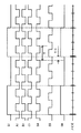
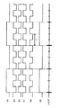
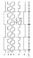
さて、本実施形態においては、電圧制御発振器3は電気的あるいは機械的な共振現象を利用したものである。このとき、定常状態における発振回路のタイミングチャートは図3で示される。電圧制御発振器3の出力クロック信号S4と、遅延回路4の出力信号S5との間には、遅延回路4の遅延量に応じた位相差が生じている。その結果として、分周回路5から出力される帰還クロック信号S6の立ち上がりエッジは、電圧制御発振器3の出力クロック信号S4の立ち上がりエッジから、一定量ずれた時点に現れる。このずれ量が、出力クロック信号S4の発振周期をTとして、T/4(または、その奇数倍)に概ね等しくなるように、遅延回路4の遅延量は調節されている。本実施形態においても、従来の発振回路と同様に、図3最下段に示されるようなスパイク状のノイズが電源電圧に重畳する。しかしながら、前述したように遅延回路4の遅延量が調節されているため、スパイク状のノイズの発生点は、電圧制御発振器3の内部信号A1,B1,C1のいずれの立ち上がりエッジ、立ち下がりエッジからも最も乖離した時点となっている。換言すると、スパイク状のノイズの発生箇所は、信号A1,B1,C1の波形がほぼ水平な時点となっている。波形が水平な状態においては、たとえノイズによって電圧制御発振器3が一時的に不安定になったとしても、その影響はすみやかに減衰し、次の立ち上がりもしくは立ち下がりエッジを揺らすには至らない。したがって、電圧制御発振器3の出力信号S4の立ち上がりエッジ、立ち下がりエッジには揺らぎが発生せず、ジッタの少ない発振回路が実現される。
【0015】
(第二の実施形態)
本発明の第二の実施形態は、前述した第一の実施形態において、電圧制御発振器3の構成のみが異なるものである。したがって、発振回路の構成例は、第一の実施形態と同様に図1で示される。
【0016】
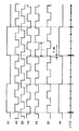
本実施形態において、電圧制御発振器3はK個のインバータ回路を環状に接続してなるリングオシレータ形式のものである。このとき、定常状態における発振回路のタイミングチャートは図4で示される。電圧制御発振器3の出力クロック信号S4と、遅延回路4の出力信号S5との間には、遅延回路4の遅延量に応じた位相差が生じている。その結果として、分周回路5から出力される帰還クロック信号S6の立ち上がりエッジは、電圧制御発振器3の出力クロック信号S4の立ち上がりエッジから、一定量ずれた時点に現れる。このずれ量が、出力クロック信号S4の発振周期をTとして、T/(4K)、または、その奇数倍に概ね等しくなるように、遅延回路4の遅延量は調節されている。本実施形態においても、従来の発振回路と同様に、図4最下段に示されるようなスパイク状のノイズが電源電圧に重畳する。しかしながら、前述したように遅延回路4の遅延量が調節されているため、スパイク状のノイズの発生箇所は、電圧制御発振器3の内部信号A2,B2,C2のいずれの立ち上がりエッジ、立ち下がりエッジからも最も乖離した時点となっている。換言すると、スパイク状のノイズの発生箇所は、信号A2,B2,C2の波形がほぼ水平な時点となっている。波形が水平な状態においては、たとえノイズによって電圧制御発振器3が一時的に不安定になったとしても、その影響はすみやかに減衰し、次の立ち上がりもしくは立ち下がりエッジを揺らすには至らない。したがって、電圧制御発振器3の出力信号S4の立ち上がりエッジ、立ち下がりエッジには揺らぎが発生せず、ジッタの少ない発振回路が実現される。
【0017】
(第三の実施形態)
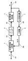
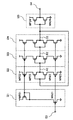
図1に示される第一および第二の実施形態においては、遅延回路4の遅延量は固定であった。しかしながら、実際の発振回路構成においては、入力クロック信号S1の周波数frや分周器5の分周数Nが可変できるように構成されているものも多い。このような場合においては、電圧制御発振器3の出力クロック信号S4の周波数foは任意の値を取りうるので、遅延回路4の遅延量もそれに連動して変化しなければ、本発明の意図する効果を得ることができない。ここで説明する第三の実施形態は、かかる状況にも対応できる構成を提供するものである。その構成例を表したブロック図を図5に示す。
【0018】
図5の構成が図1と異なるのは、遅延回路4に代えて電圧制御遅延回路6が用いられている点である。電圧制御遅延回路6は、外部電圧信号によって遅延量が変化する遅延回路であって、ここでは電圧制御発振器3の入力電圧信号S4に応じて遅延量が変化するように接続されている。いま、電圧制御発振回路3の出力クロック信号S4の周波数foは、入力電圧信号S3が高くなるに連れて上昇するように構成されているとする。このとき、電圧制御遅延回路6の遅延量が、入力電圧信号S3が高くなるに連れて低下するように設定すれば、常に出力クロック信号S4の周波数foに対して所望の遅延量を確保することが可能となる。
【0019】
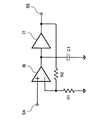
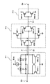
電圧制御遅延回路6は、例えば図6のような回路によって構成される。I2,I3,I4,I5は、各々インバータ回路である。このうち、I2,I3,I4の3つのインバータ回路は、出力電流が可変できるように構成されており、その値は入力電圧信号S3に応じて電圧−電流変換回路I1が生成する電流値によって決まる。すなわち、入力電圧信号S3が上昇すると、インバータ回路I2,I3,I4の出力電流が増加し、各回路における伝播遅延量が低下する。結果として、電圧制御遅延回路6の遅延量は、入力電圧信号S3が上昇するに連れて低下する。
【0020】
このようにして構成された第三の実施形態によれば、例え入力クロック信号S1の周波数frが変化したり、分周器5の分周数Nが切り替えられたりして、電圧制御発振器3の出力クロック信号S4の周波数foが変化した場合であっても、所望の遅延量が維持されるため、発振回路を広範囲に適用可能となる。
【0021】
(第四の実施形態)
第一の実施形態を実現する上で、第三の実施形態と同様の効果を得るための別法として、以下に説明する第四の実施形態がある。図7に第四の実施形態の構成例を表すブロック図を示す。
【0022】
図7の構成が図1と異なるのは、遅延回路4に代えて90度移相器7が用いられている点である。90度の移相量は時間に換算してT/4の遅延に相当するものであるから、本構成においても第一の実施形態とほぼ同様の動作が得られることは明らかである。
【0023】
90度移相器の構成例は、図8に示される。I6は電流アンプであり、入力信号S4を位相差のない電流信号に変換して出力する。電流アンプI6の出力電流は、コンデンサC1に流入する。コンデンサC1の端子間電圧は、流入する電流値を積分した値に比例する。したがって、コンデンサC1の端子間電圧は、入力信号S4より位相の90度遅れた電圧信号となる。その信号は、電圧バッファI7を通して出力される。
【0024】
本実施形態によれば、遅延量を出力クロック信号の周波数foに応じて調節することなくとも、常に所望の遅延量が得られることから、第一の実施形態に比較して回路の設計が容易になる。
【0025】
【発明の効果】
以上説明した本発明の発振回路を用いれば、位相周波数比較器1や分周器5を構成する論理回路の状態遷移によって、電源電圧や電圧制御発振器3の入力電圧信号S3にスパイク状のノイズが発生したとしても、そのスパイクの発生は、電圧制御発振器3の内部に存在するすべてのクロック信号の立ち上がりエッジ、立ち下がりエッジから最も乖離した時点となるため、電圧制御発振器3の動作は極力安定に保たれる。この結果、出力クロック信号に発生するジッタは極めて少なくなる。
【0026】
さらに、前述した第三または第四の実施形態を適用すれば、例え入力クロック信号S1の周波数frが変化したり、分周器5の分周数Nが切り替えられたりして、電圧制御発振器3の出力クロック信号S4の周波数foが変化した場合であっても、当該遅延量が所望の値を維持するように構成することができるため、発振回路を広範囲に適用することが可能となる。
【図面の簡単な説明】
【図1】本発明の第一,第二の実施形態に共通な構成例を示すブロック図。
【図2】本発明の第一,第二の実施形態に関わる遅延回路の構成例を示す図。
【図3】本発明の第一の実施形態に関わるタイミングチャート。
【図4】本発明の第二の実施形態に関わるタイミングチャート。
【図5】本発明の第三の実施形態の構成例を示すブロック図。
【図6】本発明の第三の実施形態に関わる電圧制御遅延回路の構成例を示す図。
【図7】本発明の第四の実施形態の構成例を示すブロック図。
【図8】本発明の第四の実施形態に関わる90度移相器の構成例を示す図。
【図9】従来の発振回路の構成例を示すブロック図。
【図10】従来の発振回路に関わる電圧制御発振器の構成例を示す図。
【図11】図10の電圧制御発振器を用いた従来の発振回路のタイミングチャート。
【図12】従来の発振回路に関わる電圧制御発振器の他の構成例を示す図。
【図13】図12の電圧制御発振器を用いた従来の発振回路のタイミングチャート。
【符号の説明】
1. 位相周波数比較器
2. ループフィルタ
3. 電圧制御発振器
4. 遅延回路
5. 分周器
6. 電圧制御遅延回路
7. 90度移相器[0001]
BACKGROUND OF THE INVENTION
The present invention relates to an oscillation circuit using a phase locked loop, and particularly provides a technique for reducing jitter generated in an output clock signal.
[0002]
[Prior art]
An oscillation circuit using a phase locked loop is widely used in general. A typical circuit configuration is as shown in FIG. An input clock signal S1 having a frequency fr is input to one input terminal of the
[0003]
Here, when the frequency fo / N of the feedback clock signal S6 is lower than the frequency fr of the input clock signal S1, the
[0004]
The specific configuration of the voltage-controlled
[0005]
FIG. 10 shows an example of the configuration of the voltage controlled
[0006]
On the other hand, FIG. 12 shows a configuration example of a
[0007]
[Problems to be solved by the invention]
However, in such a conventional configuration, spike-like fluctuations occur in the power supply voltage and the input voltage signal S3 of the voltage controlled
[0008]
The present invention has been made to eliminate the above-described drawbacks of the prior art, and even if the spike-like noise described above occurs, the operation of the voltage controlled
[0009]
[Means for Solving the Problems]
The oscillation circuit of the present invention solves the above-mentioned problems by inserting a delay circuit between the output of the voltage controlled
[0010]
Further, if the delay amount of the delay means is configured to be variable by the input voltage signal S3 of the voltage controlled
[0011]
DETAILED DESCRIPTION OF THE INVENTION
Hereinafter, embodiments of an oscillation circuit according to the present invention will be described in detail as first to fourth embodiments, corresponding to
[0012]
(First embodiment)
FIG. 1 is a block diagram showing a configuration example of an oscillation circuit common to the first and second embodiments of the present invention. The
[0013]
As an example, the
[0014]
In the present embodiment, the voltage-controlled
[0015]
(Second embodiment)
The second embodiment of the present invention is different from the first embodiment described above only in the configuration of the voltage controlled
[0016]
In the present embodiment, the voltage controlled
[0017]
(Third embodiment)
In the first and second embodiments shown in FIG. 1, the delay amount of the
[0018]
The configuration of FIG. 5 differs from that of FIG. 1 in that a voltage controlled
[0019]
The voltage
[0020]
According to the third embodiment configured as described above, the frequency fr of the input clock signal S1 is changed, or the frequency division number N of the
[0021]
(Fourth embodiment)
In realizing the first embodiment, there is a fourth embodiment described below as another method for obtaining the same effect as that of the third embodiment. FIG. 7 is a block diagram illustrating a configuration example of the fourth embodiment.
[0022]
The configuration of FIG. 7 differs from that of FIG. 1 in that a 90-
[0023]
A configuration example of the 90 degree phase shifter is shown in FIG. I6 is a current amplifier, which converts the input signal S4 into a current signal having no phase difference and outputs it. The output current of the current amplifier I6 flows into the capacitor C1. The voltage between the terminals of the capacitor C1 is proportional to the integrated value of the inflowing current value. Therefore, the voltage across the capacitor C1 is a voltage signal that is 90 degrees behind the phase of the input signal S4. The signal is output through the voltage buffer I7.
[0024]
According to the present embodiment, a desired delay amount can always be obtained without adjusting the delay amount according to the frequency fo of the output clock signal, so that the circuit design is easier than in the first embodiment. become.
[0025]
【The invention's effect】
When the oscillation circuit of the present invention described above is used, spike-like noise is generated in the power supply voltage or the input voltage signal S3 of the voltage controlled
[0026]
Furthermore, if the third or fourth embodiment described above is applied, the voltage controlled
[Brief description of the drawings]
FIG. 1 is a block diagram showing a configuration example common to first and second embodiments of the present invention.
FIG. 2 is a diagram showing a configuration example of a delay circuit according to the first and second embodiments of the present invention.
FIG. 3 is a timing chart according to the first embodiment of the present invention.
FIG. 4 is a timing chart according to the second embodiment of the present invention.
FIG. 5 is a block diagram showing a configuration example of a third embodiment of the present invention.
FIG. 6 is a diagram showing a configuration example of a voltage control delay circuit according to a third embodiment of the present invention.
FIG. 7 is a block diagram showing a configuration example of a fourth embodiment of the present invention.
FIG. 8 is a diagram illustrating a configuration example of a 90-degree phase shifter according to a fourth embodiment of the present invention.
FIG. 9 is a block diagram illustrating a configuration example of a conventional oscillation circuit.
FIG. 10 is a diagram showing a configuration example of a voltage controlled oscillator related to a conventional oscillation circuit.
11 is a timing chart of a conventional oscillation circuit using the voltage controlled oscillator of FIG.
FIG. 12 is a diagram showing another configuration example of a voltage controlled oscillator related to a conventional oscillation circuit.
13 is a timing chart of a conventional oscillation circuit using the voltage controlled oscillator of FIG.
[Explanation of symbols]
1. 1.
Claims (4)
Priority Applications (1)
| Application Number | Priority Date | Filing Date | Title |
|---|---|---|---|
| JP2000361557A JP3772668B2 (en) | 2000-11-28 | 2000-11-28 | Oscillation circuit using phase-locked loop |
Applications Claiming Priority (1)
| Application Number | Priority Date | Filing Date | Title |
|---|---|---|---|
| JP2000361557A JP3772668B2 (en) | 2000-11-28 | 2000-11-28 | Oscillation circuit using phase-locked loop |
Publications (3)
| Publication Number | Publication Date |
|---|---|
| JP2002164781A JP2002164781A (en) | 2002-06-07 |
| JP2002164781A5 JP2002164781A5 (en) | 2005-02-03 |
| JP3772668B2 true JP3772668B2 (en) | 2006-05-10 |
Family
ID=18832975
Family Applications (1)
| Application Number | Title | Priority Date | Filing Date |
|---|---|---|---|
| JP2000361557A Expired - Fee Related JP3772668B2 (en) | 2000-11-28 | 2000-11-28 | Oscillation circuit using phase-locked loop |
Country Status (1)
| Country | Link |
|---|---|
| JP (1) | JP3772668B2 (en) |
Families Citing this family (2)
| Publication number | Priority date | Publication date | Assignee | Title |
|---|---|---|---|---|
| JP4660076B2 (en) * | 2003-06-23 | 2011-03-30 | ルネサスエレクトロニクス株式会社 | Clock generation circuit |
| CN114826254B (en) * | 2022-06-28 | 2022-09-20 | 浙江地芯引力科技有限公司 | Phase-locked loop circuit, local oscillator and electronic equipment |
-
2000
- 2000-11-28 JP JP2000361557A patent/JP3772668B2/en not_active Expired - Fee Related
Also Published As
| Publication number | Publication date |
|---|---|
| JP2002164781A (en) | 2002-06-07 |
Similar Documents
| Publication | Publication Date | Title |
|---|---|---|
| JP2994272B2 (en) | Multi-phase clock generation circuit | |
| US6882196B2 (en) | Duty cycle corrector | |
| JP2001007698A (en) | Data PLL circuit | |
| JPH0537364A (en) | Phase locked loop | |
| CN104753499B (en) | Duty ratio calibrating circuit | |
| US10153728B2 (en) | Semiconductor device and method | |
| CN107026647A (en) | Time-to-digital system and frequency synthesizer | |
| US6774689B1 (en) | Triple input phase detector and methodology for setting delay between two sets of phase outputs | |
| CN117713807A (en) | Delay phase-locked loop circuit and multi-phase clock signal duty cycle adjustment method | |
| US7151398B2 (en) | Clock signal generators having programmable full-period clock skew control | |
| JP3772668B2 (en) | Oscillation circuit using phase-locked loop | |
| US6977539B1 (en) | Clock signal generators having programmable full-period clock skew control and methods of generating clock signals having programmable skews | |
| CN205407759U (en) | Clock duty cycle adjusting device | |
| US6657466B1 (en) | System and method for generating interleaved multi-phase outputs from a nested pair of phase locked loops | |
| KR20050011586A (en) | Delay Locked Loop For Generating Multi-Phase Clocks Without Voltage-Controlled Oscillator | |
| CN115694474B (en) | 1.5 frequency divider based on phase interpolator | |
| JP2007053685A (en) | Semiconductor integrated circuit device | |
| US7477714B2 (en) | Phase adjusting circuit for minimized irregularities at phase steps | |
| JP2001230667A (en) | Phase control circuit | |
| US10560053B2 (en) | Digital fractional frequency divider | |
| JP2010074562A (en) | Pll circuit | |
| JP2001186017A (en) | Pll circuit | |
| JP2000236241A (en) | Semiconductor integrated circuit | |
| JP2005079835A (en) | PLL oscillation circuit and electronic device using the same | |
| JP3798253B2 (en) | Phase synchronization circuit |
Legal Events
| Date | Code | Title | Description |
|---|---|---|---|
| RD04 | Notification of resignation of power of attorney |
Free format text: JAPANESE INTERMEDIATE CODE: A7424 Effective date: 20010705 |
|
| A621 | Written request for application examination |
Free format text: JAPANESE INTERMEDIATE CODE: A621 Effective date: 20040225 |
|
| A521 | Written amendment |
Free format text: JAPANESE INTERMEDIATE CODE: A523 Effective date: 20040225 |
|
| A977 | Report on retrieval |
Free format text: JAPANESE INTERMEDIATE CODE: A971007 Effective date: 20050930 |
|
| A131 | Notification of reasons for refusal |
Free format text: JAPANESE INTERMEDIATE CODE: A131 Effective date: 20051011 |
|
| A521 | Written amendment |
Free format text: JAPANESE INTERMEDIATE CODE: A523 Effective date: 20051207 |
|
| TRDD | Decision of grant or rejection written | ||
| A01 | Written decision to grant a patent or to grant a registration (utility model) |
Free format text: JAPANESE INTERMEDIATE CODE: A01 Effective date: 20060124 |
|
| A61 | First payment of annual fees (during grant procedure) |
Free format text: JAPANESE INTERMEDIATE CODE: A61 Effective date: 20060206 |
|
| R150 | Certificate of patent or registration of utility model |
Free format text: JAPANESE INTERMEDIATE CODE: R150 |
|
| FPAY | Renewal fee payment (event date is renewal date of database) |
Free format text: PAYMENT UNTIL: 20090224 Year of fee payment: 3 |
|
| FPAY | Renewal fee payment (event date is renewal date of database) |
Free format text: PAYMENT UNTIL: 20100224 Year of fee payment: 4 |
|
| FPAY | Renewal fee payment (event date is renewal date of database) |
Free format text: PAYMENT UNTIL: 20110224 Year of fee payment: 5 |
|
| FPAY | Renewal fee payment (event date is renewal date of database) |
Free format text: PAYMENT UNTIL: 20110224 Year of fee payment: 5 |
|
| FPAY | Renewal fee payment (event date is renewal date of database) |
Free format text: PAYMENT UNTIL: 20120224 Year of fee payment: 6 |
|
| FPAY | Renewal fee payment (event date is renewal date of database) |
Free format text: PAYMENT UNTIL: 20130224 Year of fee payment: 7 |
|
| FPAY | Renewal fee payment (event date is renewal date of database) |
Free format text: PAYMENT UNTIL: 20130224 Year of fee payment: 7 |
|
| S531 | Written request for registration of change of domicile |
Free format text: JAPANESE INTERMEDIATE CODE: R313531 |
|
| R350 | Written notification of registration of transfer |
Free format text: JAPANESE INTERMEDIATE CODE: R350 |
|
| LAPS | Cancellation because of no payment of annual fees |