JP3771663B2 - Electronic endoscope - Google Patents
Electronic endoscope Download PDFInfo
- Publication number
- JP3771663B2 JP3771663B2 JP08436797A JP8436797A JP3771663B2 JP 3771663 B2 JP3771663 B2 JP 3771663B2 JP 08436797 A JP08436797 A JP 08436797A JP 8436797 A JP8436797 A JP 8436797A JP 3771663 B2 JP3771663 B2 JP 3771663B2
- Authority
- JP
- Japan
- Prior art keywords
- synchronization signal
- video signal
- circuit
- electronic endoscope
- output
- Prior art date
- Legal status (The legal status is an assumption and is not a legal conclusion. Google has not performed a legal analysis and makes no representation as to the accuracy of the status listed.)
- Expired - Fee Related
Links
- 239000002131 composite material Substances 0.000 claims description 67
- 238000000034 method Methods 0.000 claims description 38
- 230000002093 peripheral effect Effects 0.000 claims description 30
- 238000001514 detection method Methods 0.000 claims description 29
- 230000008054 signal transmission Effects 0.000 description 29
- 238000010586 diagram Methods 0.000 description 8
- 230000015654 memory Effects 0.000 description 7
- 238000005070 sampling Methods 0.000 description 6
- 238000003384 imaging method Methods 0.000 description 5
- 238000006243 chemical reaction Methods 0.000 description 3
- 238000005286 illumination Methods 0.000 description 2
- 239000013307 optical fiber Substances 0.000 description 2
- 238000000926 separation method Methods 0.000 description 2
- 230000001360 synchronised effect Effects 0.000 description 2
- 238000009792 diffusion process Methods 0.000 description 1
- 230000000694 effects Effects 0.000 description 1
Images

Landscapes
- Endoscopes (AREA)
- Closed-Circuit Television Systems (AREA)
Description
【0001】
【発明の属する技術分野】
本発明は電子内視鏡に関し、一層詳しくはTVモニタ装置、ビデオテープレコーダ、プリンタ装置、画像処理装置及び医療診断装置等の周辺機器に接続し得るように構成された電子内視鏡に関する。
【0002】
【従来の技術】
周知のように、電子内視鏡は可撓性導管からなるスコープを具備し、このスコープの先端部には固体撮像デバイス例えばCCD(charge coupled device)イメージセンサが設けられ、このCCDイメージセンサは対物レンズ系と組み合わされる。また、かかるスコープ内には光ファイバー束からなる照明用光ガイドが挿通させられ、その先端部の端面は電子内視鏡のスコープの先端に位置し、その他方の端部は光源に接続させられる。患者の体腔内へのスコープの挿入時にその先端側の対物レンズ系の前方が光ガイドの先端部端面からの射出光でもって照明され、これにより対物レンズ系によって捉えられた被写体像は固体撮像デバイスの受光面に結像させられる。電子内視鏡は更に固定撮像デバイスで得られる映像信号を処理してビデオ信号を作成するプロセッサを具備し、このビデオ信号に基づいてTVモニタ装置上で映像が再現される。
【0003】
通常は、電子内視鏡はカラーモニタ装置と組み合わされて、フルカラー映像を再現するように構成される。電子内視鏡で用いるCCDイメージセンサ等の固体撮像デバイスの画素数は通常のTV用固体撮像素子の画素数に比べて少ないので、いわゆる面順次方式が採用される。即ち、光源と照明用光ガイドとの間には例えば回転式RGBカラーフィルタが介在させられ、その光ガイドの先端の端面からは赤色光、緑色光及び青色光が順次射出させられ、被写体像が赤色光、緑色光及び青色光でもってCCDイメージセンサの受光面に順次結像され、そこから赤色画像信号、緑色画像信号及び青色画像信号が所定の時間間隔で読み出される。次いで、個々の色の映像信号は上述のプロセッサで処理されてカラービデオ信号とされ、このカラービデオ信号に基づいてフルカラー映像がカラーモニタ装置上で再現される。
【0004】
近年、電子内視鏡で得られる映像信号については、映像再現のためにTVモニタ装置だけで使用するのではなく、その他の周辺機器例えばビデオテープレコーダ、プリンタ装置、画像処理装置及び医療診断装置等でも使用することが望まれている。このような周辺機器では、通常は画質の良いコンポーネントビデオ信号が用いられるようになっている。従って、電子内視鏡に適当な複数の接続端子を設け、それら接続端子を介して個々の周辺機器にコンポーネントビデオ信号を送ればよいことになる。
【0005】
【発明が解決しようとする課題】
ところが、従来の電子内視鏡においては、コンポーネントビデオ信号の一成分である複合同期信号の振幅レベルは所定値に固定され、このため周辺機器によってはコンポーネントビデオ信号のその他の信号成分の処理を適正に行い得ないということが問題とされる。更に、或る周辺機器にあっては、複合同期信号の極性を反転したものが必要とされる場合もある。従って、従来では、個々の周辺機器側で電子内視鏡からの複合同期信号を処理してその周辺機器に適合した同期信号を得る同期信号処理装置を予め用意することが必要であり、このため周辺機器を直ちに利用し得ないとう点が問題となる。
【0006】
従って、本発明の目的は上述したようなタイプの電子内視鏡であって、個々の周辺機器に適合し得る複合同期信号を少なくとも2種類以上出力し得るように構成された電子内視鏡を提供することである。
【0007】
【課題を解決するための手段】
本発明による電子内視鏡はコンポーネントビデオ信号を出力するように構成されるものであって、該コンポーネントビデオ信号の一成分となる複合同期信号を処理して異なった振幅値を持つ少なくとも2種類の複合同期信号を出力させるための同期信号処理回路を具備して成るものである。
【0008】
本発明による電子内視鏡にあっては、好ましくは、同期信号処理回路は更に極性を反転した複合同期信号を出力し得るように構成され、更に好ましくは同期信号処理回路は水平同期信号及び垂直同期信号を出力するようにも構成される。
【0009】
また、本発明による電子内視鏡にあっては、同期信号処理回路の出力端子に対する周辺機器の接続を検出するようになった検出回路を設けてもよく、この場合には、更に、同期信号処理回路のどの出力端子が周辺機器に接続されたかが検出回路によって検出された際にその検出された出力端子を認識させるための情報を表示する表示手段が設けられてもよい。
【0010】
【発明の実施の形態】
次に、本発明による電子内視鏡の一実施形態について添付図面を参照して説明する。
【0011】
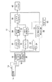
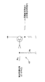
図1を参照すると、本発明による電子内視鏡の一実施形態がブロック図として示される。電子内視鏡は可撓性導管からなるスコープ10及びビデオ信号処理装置12を具備し、スコープ10はビデオ信号処理装置に着脱自在に接続されるようになっている。
【0012】
スコープ10の先端部即ち遠位端にはCCDイメージセンサ14が設けられ、このCCDイメージセンサ14は対物レンズ系(図示されない)と組み合わされ、この対物レンズ系によって撮られた被写体像がCCDイメージセンサ14の受光面に結像させられる。CCDイメージセンサ14によって得られたビデオ信号はCCDドライブ回路16によって読み出され、そのビデオ信号はビデオ信号処理装置12に取り込まれる。
【0013】
また、スコープ10内には光ファイバー束からなる光ガイド18が挿通させられ、この光ガイド18の遠位端はスコープ10の遠位端まで延びる。光ガイド18の近位端はビデオ信号処理装置12へのスコープ10の接続時にビデオ信号処理装置12内の光ガイド20の外側端に接続され、光ガイド20の内側端は光源22に接続させられる。
【0014】
本実施形態では、電子内視鏡は面順次方式によるカラー映像を再現し得るように構成されるので、光ガイド20の内側端と光源22との間には回転式三原色カラーフィルタとしてRGBカラーフィルタ24がが介在させられ、光源22からの光は光ガイド20の内側端面に集光させられる。RGBカラーフィルタ24が所定の回転周波数例えば25Hz(PAL方式) 或いは30Hz(NTSC方式)で回転させられると、被写体は赤色光(R)、緑色光(G)及び青色光(B)によって順次照明され、被写体はそれぞれの色の光によりCCDイメージセンサ14の受光面に順次結像される。
【0015】
更に、スコープ10内には適当な読出し専用メモリ例えば書込み可能な読出し専用メモリ(EEPROM)26が設けられ、このEEPROM26にはスコープ10に組み込まれたCCDイメージセンサ14についての種々の情報データが書き込まれる。例えば、CCDイメージセンサ14からCCDドライブ回路16によって読み出されるアナログビデオ信号をデジタルビデオ信号に変換すべき際のサンプリング周波数等の情報データ等がEEPROM26に保持される。
【0016】
ビデオ信号処理装置12にはシステムコントロール回路28が設けられ、このシステムコントロール回路28は例えば中央演算装置(CPU)等のマイクロプロセッサ及びメモリ(ROM、RAM)等からなるマイクロコンピュータとして構成される。スコープ10がビデオ信号処理装置12に接続されると、システムコントロール回路28は先ずドライブ回路30を介してEEPROM26の情報データを取り込む。また、システムコントロール回路28はCCDプロセス回路32、タイミング回路34及びビデオプロセス回路36を制御するようになっている。
【0017】
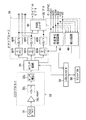
図2に示すように、CCDプロセス回路32には、CCDイメージセンサ14からCCDドライブ回路16によって順次読み出される赤色ビデオ信号、緑色ビデオ信号及び青色ビデオ信号を増幅する増幅器321 と、増幅器321 からビデオ信号をサンプリングするサンプルホールド(S/H)回路322 と、このサンプルホールド回路322 から出力されるビデオ信号にガンマ補正処理を施すガンマ補正処理回路323 とが設けられる。ガンマ補正処理回路323 で処理された赤色ビデオ信号、緑色ビデオ信号及び青色ビデオ信号の各々はタイミング回路34に対して順次出力される。
【0018】
タイミング回路34内にはアナログ/デジタル変換器及びタイミングジェネレータが含まれ、該タイミングジェネレータからは該アナログ/デジタル変換にサンプリング用クロックパルスが出力され、CCDプロセス回路32からの各色のビデオ信号(アナログ)はサンプリング用クロックパルスに基づいて該アナログ/デジタル変換器によってデジタルビデオ信号に変換される。タイミング回路34内のタイミングジェネレータはシステムコントロール回路28によって制御され、該タイミングジェネレータから出力されるサンプリング用クロックパルスの周波数はEEPROM26から読み出された情報データに基づいて決められる。
【0019】
なお、タイミング回路34内のタイミングジェネレータからはCCDプロセス回路32のS/H回路322 及びガンマ補正回路323 にも所定周波数のクロックパルスが出力され、それらクロックパルスに従ってS/H回路322 での各色のビデオ信号のサンプリングのタイミング及びガンマ補正回路323 のガンマ処理のタイミングが制御される。
【0020】
タイミング回路34内のアナログ/デジタル変換器から順次出力される赤色デジタルビデオ信号(R)、緑色デジタルビデオ信号(G)及び青色デジタルビデオ信号(B)はビデオプロセス回路36内のメモリ38R、38G及び38Bにそれぞれ書き込まれる。図2に示すように、ビデオプロセス回路36にはメモリ38R、38G及び38Bのそれぞれに接続されたデジタル/アナログ変換器(D/A)40R、40G及び40Bが設けられ、メモリ38R、38G及び38Bのそれぞれから読み出された赤色デジタルビデオ信号(R)、緑色デジタルビデオ信号(G)及び青色デジタルビデオ信号(B)はD/A変換器40R、40G及び40Bによって赤色アナログビデオ信号(R)、緑色アナログビデオ信号(G)及び青色アナログビデオ信号(B)に戻されてビデオプロセス回路36から出力される。
【0021】
なお、各メモリ38R、38G、38Bへのデジタルビデオ信号の書込み及びそこからのデジタルビデオ信号の読出しタイミングについてはタイミング回路34内のタイミングジェネレータからの所定周波数のクロックパルスに従って行われ、また各D/A変換40R、40G、40Bでのデジタルビデオ信号からアナログ信号への変換タイミングについてもタイミング回路34内のタイミングジェネレータからの所定周波数のクロックパルスに従って行われる。
【0022】
また、ビデオプロセス回路36には同期信号処理回路42が設けられ、この同期信号処理回路42にはタイミング回路34のタイミングジェネレータから得られる複合同期信号(C−SYNC)が入力させられる。本発明によれば、タイミング回路34からの複合同期信号(C−SYNC)は同期信号処理回路42に入力されて少なくとも2種類以上の異なった振幅値を持つ複合同期信号として出力される。
【0023】
本実施形態にあっては、図2から明らかなように、同期信号処理回路42からは、高レベルの振幅値を持つ複合同期信号(HIGH)と、中間レベルの振幅値を持つ複合同期信号(MID)と、低レベルの振幅値を持つ複合同期信号(LOW)と、高レベルの振幅値を持ちしかも反転された複合同期信号(INV)と、水平同期信号(HD)と、垂直同期信号(VD)とが出力される。例えば、図3に示すように、高レベルの振幅値としては4ボルト(peak-to-peak)が、中間レベルの振幅値としては2ボルト(peak-to-peak)が、低レベルの振幅値としては1ボルト(peak-to-peak)が与えられる。
【0024】
なお、同期信号処理回路42からは、必要に応じて、中間レベルの振幅値を持ちしかも反転された複合同期信号並びに低レベルの振幅値を持ちしかも極性の反転された複合同期信号を出力するようにしてもよく、また上述したレベル以外の振幅値を持つ複合同期信号及びその反転信号をを出力するようにしてもよいことは勿論である。
【0025】
同期信号処理回路42には、高レベルの振幅値を持つ複合同期信号(HIGH)、中間レベルの振幅値を持つ複合同期信号(MID)及び低レベルの振幅値を持つ複合同期信号(LOW)を得るために、図4に示すような振幅値変更回路素子43、即ちトランジスタと入力分圧抵抗との組合から成る振幅値変更回路素子43が3つ設けられる。
【0026】
例えば、タイミング回路34のタイミングジェネレータから得られる複合同期信号(C−SYNC)の振幅電圧が4ボルト(peak-to-peak)であるとすると、一方の分圧抵抗の抵抗値Ra と他方の分圧抵抗の抵抗値Rb とが等しい場合には、振幅値変更回路素子43から出力される複合同期信号の振幅電圧は入力電圧4ボルトの半分の電圧値2ボルトに変更される。
【0027】
また、一方の分圧抵抗の抵抗値Ra が他方の分圧抵抗の抵抗値Rb よりも小さい場合には、振幅値変更回路素子43から出力される複合同期信号の振幅電圧は入力電圧4ボルトの半分の電圧値2ボルトよりも大きな電圧値に変更される。例えば、Ra =0であれば、振幅値変更回路素子43から出力される複合同期信号の振幅電圧は入力電圧値と同じ4ボルトとなる。
【0028】
更に、一方の分圧抵抗の抵抗値Ra が他方の分圧抵抗の抵抗値Rb よりも大きい場合には、振幅値変更回路素子43から出力される複合同期信号の振幅電圧は入力電圧4ボルトの半分の電圧値2ボルトよりも小さな電圧値に変更される。例えば、Ra =3Rb であれば、振幅値変更回路素子43から出力される複合同期信号の振幅電圧は1ボルトとなる。
【0029】
また、同期信号処理回路42には、高レベルの振幅値を持ちしかも極性の反転された複合同期信号(IVN)を得るために、図5に示すような振幅値変更回路素子43′、即ちトランジスタと、入力分圧抵抗と、インバータとの組合から成る振幅値変更回路素子43′が設けられる。同図から明らかように、タイミング回路34からの複合同期信号はインバータのためにその極性を反転させてトランジスタのベース側に入力されるので、該振幅値変更回路素子43′から得られる複合同期信号もその極性が反転されたものとなる。
【0030】
同期信号処理回路42には更に同期信号分離回路も設けられ、この同期信号分離回路により、タイミング回路34からの複合同期信号は水平同期信号(HD)及び垂直同期信号(VD)に分離されて該同期信号処理回路42から出力されることになる。
【0031】
要するに、本実施形態では、4つの複合同期信号(HIGH,MID,LOW,INV)のうちのいずれか1つと、赤色アナログビデオ信号(R)、緑色アナログビデオ信号(G)及び青色アナログビデオ信号(B)との組合から成る4種類のコンポーネント信号、並びに水平同期信号(HD)及び垂直同期信号(VD)から成る一組の同期信号と、赤色アナログビデオ信号(R)、緑色アナログビデオ信号(G)及び青色アナログビデオ信号(B)との組合から成る1種類のコンポーネント信号の合計5種類のコンポーネントビデオ信号がビデオプロセス回路36から外部即ち周辺機器に対して出力されるようになっている。
【0032】
本実施形態においては、ビデオプロセス回路36には更にまたRGBエンコーダ44が設けられ、このRGBエンコーダ44には、D/A変換器40R、40G及び40Bからの赤色アナログビデオ信号(R)、緑色アナログビデオ信号(G)及び青色アナログビデオ信号(B)とタイミング回路34からの複合同期信号(C−SYNC)とが入力され、これら信号に基づいてSビデオ信号及びコンポジットビデオ信号が作成され、これらビデオ信号はRGBエンコーダ44即ちビデオプロセス回路36から外部即ち周辺機器に対して出力されるようになっている。
【0033】
以上で述べた種々のビデオ信号のうちの1つは図1に示すようにTVモニタ装置46に送られ、そこでスコープ10のCCD14で捉えられた映像が再現されることになる。また、本発明による電子内視鏡にあっては、TVモニタ装置46以外のTVモニタ装置やその他の周辺機器、例えばビデオテープレコーダ、プリンタ装置、画像処理装置及び医療診断装置等にもコンポーネントビデオ信号を送り得るようになっており、このとき該コンポーネントビデオ信号には個々の周辺機器に適合したレベルの振幅値を持つ複合同期信号が含まれることになる。
【0034】
このような場合、どのレベルの振幅値を持つ複合同期信号が電子内視鏡から出力されているかを直ちに知ることが好ましい。そこで本実施形態では、図2に示すように、ビデオプロセス回路36には検出回路48が設けられ、この検出回路48によって複合同期信号の接続端子のいずれかがビデオ信号送信用ケーブルに接続されているか否かが検出され、その検出結果がビデオ信号処理装置12のフロントパネル50に表示されるようになっている。
【0035】
先ず、検出回路48について説明すると、図6に示すように、検出回路48には検出回路素子49が設けられ、この検出回路素子49は比較器491 を包含する。比較器491 の一方の入力端子は同期信号処理回路42の振幅値変更回路素子43の出力端子側に接続され、その他方の入力端子は閾値電圧を規定する電源492 に接続される。図6から明らかなように、振幅値変更回路素子43の出力端子側の接続コネクタ421 に周辺機器からのビデオ信号送信用ケーブル側の接続コネクタが422 が接続されると、ビデオ信号送信用ケーブル側の接続コネクタ422 の接地側に設けた抵抗のために振幅値変更回路素子43の出力側の電位が降下し、この降下電位を比較器491 で電源492 からの閾値電圧と比較することにより、振幅値変更回路素子43の出力端子側の接続コネクタ421 に対するビデオ信号送信用ケーブル側のコネクタ422 の接続の有無を検出することができる。
【0036】
例えば、図6に示す振幅値変更回路素子43の出力端子から高レベルの振幅値を持つ複合同期信号(HIGH)が出力され、しかもその出力電位即ち4ボルトが2ボルトまで電圧降下すると仮定した場合には、電源492 からの閾値電圧は3ボルトに設定される。コネクタ421 にコネクタ422 が接続されていないとき、即ち閾値電圧3ボルトよりも高い振幅値変更回路素43の出力端子の電圧4ボルトが比較器491 に印加されているときには、例えば比較器491 からは零ボルトが出力され、一方コネクタ421 にコネクタ422 が接続されたとき、即ち閾値電圧3ボルトよりも低い振幅値変更回路素43の出力端子の電圧2ボルトが比較器491 に印加されているときには、例えば比較器491 からは高レベルの電圧5ボルトが出力されるようになっている。
【0037】
なお、以上に述べた場合と同様な態様で、同期信号処理回路42のその他の出力端子、即ち中間レベルの振幅値を持つ複合同期信号(MID)、低レベルの振幅値を持つ複合同期信号(LOW)、高レベルの振幅値を持ちしかも反転された複合同期信号(INV)、水平同期信号(HD)及び垂直同期信号(VD)が出力される出力端子についても周辺機器からのビデオ信号送信用ケーブル側のコネクタの接続に対する接続の有無を検出することが可能である。
【0038】
図6で述べた例にあっては、同期信号処理回路42の出力端子のそれぞれに検出回路素子49が設けられる方式を採用しているが、しかし単一の検出回路素子49を同期信号処理回路42の6つの出力端子のすべてに共有することも可能である。この場合には、比較器491 の一方の入力端子は例えばマルチプレクサ(図示されない)を介して同期信号処理回路42の6つの出力端子に順次接続させられ、その接続に応じて電源492 からの閾値電圧が変更させられる。このような方式を採用した場合には、検出回路48からの出力端子は1つとすることができる。
【0039】
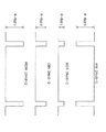
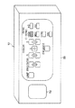
一方、図7に示すように、ビデオ信号処理装置12のフロントパネル50には英文字“HIGH”、“MID”、“LOW”、“INV”、“HD”及び“VD”で示される表示窓が配置され、これら表示窓は半透明板あるいは光拡散板として形成され、各表示窓の内側には適当な光源例えば発光ダイオード(LED)が設けられる。表示窓“HIGH”、“MID”、“LOW”、“INV”、“HD”及び“VD”はそれぞれ複合同期信号(HIGH)、複合同期信号(MID)、複合同期信号(LOW)、反転複合同期信号(INV)、水平同期信号(HD)及び垂直同期(VD)に対応する。
【0040】
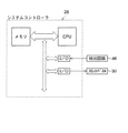
図8に示すように、検出回路48の出力端子は入出力ポート(I/O)を介してシステムコントロール回路28のCPUに接続され、また該CPUは入出力ポート(I/O)を介してフロントパネル50の表示窓“HIGH”、“MID”、“LOW”、“INV”、“HD”及び“VD”内の発光ダイオードの電源回路のそれぞれに接続される。なお、図8では、検出回路48には単一の検出回路素子49が設けられ、その単一の検出回路素子49が同期信号処理回路42の6つの出力端子のすべてに共有されているものとされており、このため検出回路48からの出力端子は1つとされ、その出力端子に対して一つの入出力ポート(I/O)が充てられているが、もちろん同期信号処理回路42の6つの出力端子のそれぞれに検出回路素子49を接続した場合には、それら6つの検出回路素子49の出力端子はそれぞれ6つの入出力ポート(I/O)を介してシステムコントロール回路28のCPUに接続されることになる。
【0041】
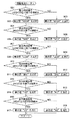
図9にはシステムコントロール回路28のCPUで実行される接続検出ルーチンのフローチャートが示される。なお、接続検出ルーチンは所定の時間間隔例えば30ms毎に実行される割込みルーチンとされる。
【0042】
ステップ901では、同期信号処理回路42の6つの出力端子のうちの複合同期信号(HIGH)の出力端子が周辺機器からのビデオ信号送信用ケーブルが接続されたか否かが判断される。ステップ901で複合同期信号(HIGH)の出力端子に対するビデオ信号送信用ケーブルの接続が確認されると、ステップ902に進み、そこで表示窓“HIGH”が点灯される。一方、ステップ901で複合同期信号(HIGH)の出力端子に対するビデオ信号送信用ケーブルの接続が確認されていない場合あるいは複合同期信号(HIGH)の出力端子に対してビデオ信号送信用ケーブルが一旦接続された後にその接続が外された場合には、ステップ901からステップ903に進み、そこで表示窓“HIGH”は消灯される。
【0043】
ステップ904では、同期信号処理回路42の6つの出力端子のうちの複合同期信号(MID)の出力端子が周辺機器からのビデオ信号送信用ケーブルが接続されたか否かが判断される。ステップ904で複合同期信号(MID)の出力端子に対するビデオ信号送信用ケーブルの接続が確認されると、ステップ905に進み、そこで表示窓“MID”が点灯される。一方、ステップ904で複合同期信号(MID)の出力端子に対するビデオ信号送信用ケーブルの接続が確認されていない場合あるいは複合同期信号(MID)の出力端子に対してビデオ信号送信用ケーブルが一旦接続された後にその接続が外された場合には、ステップ904からステップ906に進み、そこで表示窓“MID”は消灯される。
【0044】
ステップ907では、同期信号処理回路42の6つの出力端子のうちの複合同期信号(LOW)の出力端子が周辺機器からのビデオ信号送信用ケーブルが接続されたか否かが判断される。ステップ907で複合同期信号(LOW)の出力端子に対するビデオ信号送信用ケーブルの接続が確認されると、ステップ908に進み、そこで表示窓“LOW”が点灯される。一方、ステップ907で複合同期信号(LOW)の出力端子に対するビデオ信号送信用ケーブルの接続が確認されていない場合あるいは複合同期信号(LOW)の出力端子に対してビデオ信号送信用ケーブルが一旦接続された後にその接続が外された場合には、ステップ907からステップ909に進み、そこで表示窓“LOW”は消灯される。
【0045】
ステップ910では、同期信号処理回路42の6つの出力端子のうちの複合同期信号(INV)の出力端子が周辺機器からのビデオ信号送信用ケーブルが接続されたか否かが判断される。ステップ910で複合同期信号(INV)の出力端子に対するビデオ信号送信用ケーブルの接続が確認されると、ステップ911に進み、そこで表示窓“INV”が点灯される。一方、ステップ910で複合同期信号(INV)の出力端子に対するビデオ信号送信用ケーブルの接続が確認されていない場合あるいは複合同期信号(INV)の出力端子に対してビデオ信号送信用ケーブルが一旦接続された後にその接続が外された場合には、ステップ910からステップ912に進み、そこで表示窓“INV”は消灯される。
【0046】
ステップ913では、同期信号処理回路42の6つの出力端子のうちの水平同期信号(HD)の出力端子が周辺機器からのビデオ信号送信用ケーブルが接続されたか否かが判断される。ステップ913で水平同期信号(HD)の出力端子に対するビデオ信号送信用ケーブルの接続が確認されると、ステップ914に進み、そこで表示窓“HD”が点灯される。一方、ステップ913で水平同期信号(HD)の出力端子に対するビデオ信号送信用ケーブルの接続が確認されていない場合あるいは水平同期信号(HD)の出力端子に対してビデオ信号送信用ケーブルが一旦接続された後にその接続が外された場合には、ステップ913からステップ915に進み、そこで表示窓“HD”は消灯される。
【0047】
ステップ916では、同期信号処理回路42の6つの出力端子のうちの垂直同期信号(VD)の出力端子が周辺機器からのビデオ信号送信用ケーブルが接続されたか否かが判断される。ステップ916で垂直同期信号(VD)の出力端子に対するビデオ信号送信用ケーブルの接続が確認されると、ステップ917に進み、そこで表示窓“VD”が点灯される。一方、ステップ916で垂直同期信号(VD)の出力端子に対するビデオ信号送信用ケーブルの接続が確認されていない場合あるいは垂直同期信号(VD)の出力端子に対してビデオ信号送信用ケーブルが一旦接続された後にその接続が外された場合には、ステップ916からステップ918に進み、そこで表示窓“VD”は消灯される。
【0048】
上述したように、単一の検出回路素子49を同期信号処理回路42の6つの出力端子のすべてに共有した場合には、比較器491 の一方の入力端子はマルチプレクサ(図示されない)を介して同期信号処理回路42の6つの出力端子に順次接続させられることになるが、それら6つの出力端子に対する接続切換については接続検出ルーチンの割込み時間間隔30msよりも大幅に短い時間例えば6msで一巡するようになっているので、同期信号処理回路42の6つの出力端子のうちのどの出力端子に周辺機器からのビデオ信号送信用ケーブルが接続されたかを判断することことが可能である。
【0049】
なお、図7に示すように、フロントパネル50には表示窓“HIGH”、“MID”、“LOW”、“INV”、“HD”及び“VD”の他に種々のスイッチも設けられるが、それら種々のスイッチ自体は本発明とは直接的には関係しないものであるので、以下に簡単に説明する。
【0050】
英文字“R”、“G”及び“B”で示されるスイッチはカラー調整スイッチであり、“R”、“G”及び“B”はそれぞれ赤色、緑色及び青色に対応する。英文字“ENHANCE”で示されるスイッチは輪郭強調スイッチであり、この輪郭強調スイッチがONされると、ビデオ信号に輪郭強調処理が施される。英文字“BRIGHTNESS”で示されるスイッチは再現映像の輝度を調節するものである。英文字“LAMP”で示されるスイッチは光源22のオン/オフスイッチである。また、フロントパネル50の左側に設けられたスイッチ52は電子内視鏡のメインスイッチである。
【0051】
図1を参照すると、上述したような種々のスイッチはフロントパネル50の一部に纏めてパネルスイッチ54として示されている。また、図1から明らかように、システムコントロール回路28にはキーボード56が接続され、このキーボード56を介して種々の指令信号や指令データ等がシステムコントロール回路28に対して入力されるようになっている。
【0052】
【発明の効果】
以上の記載から明らかように、本発明による電子内視鏡にあっては、個々の周辺機器に適合し得るように異なった振幅値を持つ複合同期信号が少なくとも2系統以上出力し得るようになっているので、本発明によれば、種々の周辺機器を効果的にかつ容易に利用し得るという利点が得られる。また、本発明による電子内視鏡が極性を反転した複合同期信号を出力し得るように構成された場合には、周辺機器の効果的な利用性が更に高められる。
【図面の簡単な説明】
【図1】本発明による電子内視鏡の概略ブロック図である。
【図2】図1のCCDプロセス回路及びビデオプロセス回路を更に詳細に示すブロック図である。
【図3】図2の同期信号処理回路から出力される複合同期信号の種類を示す波形図である。
【図4】図2の同期信号処理回路に含まれる振幅値変更回路素子の構成図である。
【図5】図2の同期信号処理回路に含まれる別の振幅値変更回路素子であって、複合同期信号の極性を反転させるようになった振幅値変更回路素子の構成図である。
【図6】図2の同期信号処理回路及び検出回路の構成図である。
【図7】図1に示したビデオ信号処理装置の斜視図であって、そのフロントパネルを示す図である。
【図8】システムコントロール回路の詳細図であって、そのシステムコントロール回路と検出回路とフロントパネルとの関係を示す図である。
【図9】図8のシステムコントロール回路のCPUで実行される接続検出ルーチンを示すフローチャートである。
【符号の説明】
10 スコープ
12 ビデオ信号処理装置
16 CCDドライブ回路
18 光ガイド
20 光ガイド
28 システムコントロール回路
32 CCDプロセス回路
34 タイミング回路
36 ビデオプロセス回路
42 同期信号処理回路
48 検出回路
50 フロントパネル[0001]
BACKGROUND OF THE INVENTION
The present invention relates to an electronic endoscope, and more particularly to an electronic endoscope configured to be connected to peripheral devices such as a TV monitor device, a video tape recorder, a printer device, an image processing device, and a medical diagnostic device.
[0002]
[Prior art]
As is well known, an electronic endoscope includes a scope formed of a flexible conduit, and a solid-state imaging device such as a charge coupled device (CCD) image sensor is provided at the distal end of the scope. Combined with the lens system. Further, an illumination light guide made of a bundle of optical fibers is inserted into the scope, the end surface of the distal end thereof is located at the distal end of the scope of the electronic endoscope, and the other end is connected to the light source. When the scope is inserted into the body cavity of the patient, the front of the objective lens system on the distal end side is illuminated with the light emitted from the end face of the distal end of the light guide, so that the subject image captured by the objective lens system is a solid-state imaging device The image is formed on the light receiving surface. The electronic endoscope further includes a processor that processes a video signal obtained by the fixed imaging device to generate a video signal, and a video is reproduced on the TV monitor device based on the video signal.
[0003]
Normally, an electronic endoscope is configured to reproduce a full-color image in combination with a color monitor device. Since the number of pixels of a solid-state imaging device such as a CCD image sensor used in an electronic endoscope is smaller than the number of pixels of a normal TV solid-state imaging device, a so-called frame sequential method is adopted. That is, for example, a rotary RGB color filter is interposed between the light source and the illumination light guide, and red light, green light, and blue light are sequentially emitted from the end face of the light guide, and the subject image is displayed. Images are sequentially formed on the light receiving surface of the CCD image sensor with red light, green light, and blue light, from which red image signals, green image signals, and blue image signals are read out at predetermined time intervals. Next, each color video signal is processed by the above-described processor to be a color video signal, and a full color video is reproduced on the color monitor device based on the color video signal.
[0004]
In recent years, video signals obtained by electronic endoscopes are not used only by TV monitor devices for video reproduction, but are also used for other peripheral devices such as video tape recorders, printer devices, image processing devices, medical diagnostic devices, etc. But it is desired to use. In such a peripheral device, a component video signal with high image quality is usually used. Therefore, it is only necessary to provide a plurality of appropriate connection terminals for the electronic endoscope and send component video signals to individual peripheral devices via these connection terminals.
[0005]
[Problems to be solved by the invention]
However, in the conventional electronic endoscope, the amplitude level of the composite sync signal, which is one component of the component video signal, is fixed to a predetermined value, and depending on the peripheral device, the processing of other signal components of the component video signal is appropriate. The problem is that it cannot be done. Further, some peripheral devices may require a composite sync signal with the polarity reversed. Therefore, conventionally, it is necessary to prepare in advance a synchronization signal processing device that processes a composite synchronization signal from an electronic endoscope on each peripheral device side and obtains a synchronization signal suitable for the peripheral device. The problem is that peripheral devices cannot be used immediately.
[0006]
Accordingly, an object of the present invention is an electronic endoscope of the type described above, and an electronic endoscope configured to output at least two types of composite synchronization signals that can be adapted to individual peripheral devices. Is to provide.
[0007]
[Means for Solving the Problems]
An electronic endoscope according to the present invention is configured to output a component video signal, and processes at least two kinds of amplitude values having different amplitude values by processing a composite synchronizing signal which is one component of the component video signal. A synchronization signal processing circuit for outputting a composite synchronization signal is provided.
[0008]
In the electronic endoscope according to the present invention, it is preferable that the synchronization signal processing circuit is configured to output a composite synchronization signal whose polarity is further inverted, and more preferably, the synchronization signal processing circuit is configured to output the horizontal synchronization signal and the vertical synchronization signal. It is also configured to output a synchronization signal.
[0009]
In the electronic endoscope according to the present invention, a detection circuit adapted to detect connection of a peripheral device to the output terminal of the synchronization signal processing circuit may be provided. Display means may be provided for displaying information for recognizing the detected output terminal when the detection circuit detects which output terminal of the processing circuit is connected to the peripheral device.
[0010]
DETAILED DESCRIPTION OF THE INVENTION
Next, an embodiment of an electronic endoscope according to the present invention will be described with reference to the accompanying drawings.
[0011]
Referring to FIG. 1, an embodiment of an electronic endoscope according to the present invention is shown as a block diagram. The electronic endoscope includes a
[0012]
A
[0013]
Further, a
[0014]
In the present embodiment, since the electronic endoscope is configured to reproduce a color image by the frame sequential method, an RGB color filter is provided as a rotary three primary color filter between the inner end of the
[0015]
Further, an appropriate read-only memory such as a writable read-only memory (EEPROM) 26 is provided in the
[0016]
The video
[0017]
As shown in FIG. 2, the
[0018]
The
[0019]
The timing generator in the
[0020]
A red digital video signal (R), a green digital video signal (G), and a blue digital video signal (B) sequentially output from the analog / digital converter in the
[0021]
Note that the writing timing of the digital video signal to each of the
[0022]
The
[0023]
In the present embodiment, as is apparent from FIG. 2, the synchronization
[0024]
The sync
[0025]
The synchronization
[0026]
For example, when the amplitude voltage of the composite synchronization signal (C-SYNC) obtained from the timing generator of the
[0027]
Also, the resistance value R of one voltage dividing resistor a Is the resistance value R of the other voltage dividing resistor b Is smaller than that, the amplitude voltage of the composite synchronizing signal output from the amplitude value changing
[0028]
Further, the resistance value R of one voltage dividing resistor a Is the resistance value R of the other voltage dividing resistor b Is larger than that, the amplitude voltage of the composite synchronizing signal output from the amplitude value changing
[0029]
Further, in order to obtain a composite synchronizing signal (IVN) having a high level amplitude value and having an inverted polarity, the synchronizing
[0030]
The synchronization
[0031]
In short, in this embodiment, any one of the four composite synchronization signals (HIGH, MID, LOW, INV), the red analog video signal (R), the green analog video signal (G), and the blue analog video signal ( B) four types of component signals, a set of synchronizing signals consisting of a horizontal synchronizing signal (HD) and a vertical synchronizing signal (VD), a red analog video signal (R), and a green analog video signal (G ) And a blue analog video signal (B), a total of five types of component video signals are output from the
[0032]
In the present embodiment, the
[0033]
One of the various video signals described above is sent to the
[0034]
In such a case, it is preferable to immediately know which level of the amplitude value of the composite synchronization signal is output from the electronic endoscope. Therefore, in this embodiment, as shown in FIG. 2, the
[0035]
First, the
[0036]
For example, assuming that a composite synchronizing signal (HIGH) having a high level amplitude value is output from the output terminal of the amplitude value changing
[0037]
In the same manner as described above, the other output terminals of the sync
[0038]
In the example described with reference to FIG. 6, the
[0039]
On the other hand, as shown in FIG. 7, the
[0040]
As shown in FIG. 8, the output terminal of the
[0041]
FIG. 9 shows a flowchart of a connection detection routine executed by the CPU of the
[0042]
In
[0043]
In
[0044]
In
[0045]
In
[0046]
In
[0047]
In
[0048]
As described above, when the single
[0049]
As shown in FIG. 7, the
[0050]
The switches indicated by the letters “R”, “G”, and “B” are color adjustment switches, and “R”, “G”, and “B” correspond to red, green, and blue, respectively. The switch indicated by the English characters “ENHANCE” is a contour emphasis switch. When this contour emphasis switch is turned on, a contour emphasis process is performed on the video signal. The switch indicated by the English characters “BRIGHTNESS” adjusts the brightness of the reproduced image. A switch indicated by an English letter “LAMP” is an on / off switch of the
[0051]
Referring to FIG. 1, the various switches as described above are collectively shown as a
[0052]
【The invention's effect】
As is apparent from the above description, the electronic endoscope according to the present invention can output at least two or more composite synchronization signals having different amplitude values so as to be adapted to individual peripheral devices. Therefore, according to the present invention, there is an advantage that various peripheral devices can be used effectively and easily. In addition, when the electronic endoscope according to the present invention is configured so as to output a composite synchronizing signal with reversed polarity, the effective usability of peripheral devices can be further enhanced.
[Brief description of the drawings]
FIG. 1 is a schematic block diagram of an electronic endoscope according to the present invention.
FIG. 2 is a block diagram showing the CCD process circuit and video process circuit of FIG. 1 in more detail.
FIG. 3 is a waveform diagram showing types of composite synchronization signals output from the synchronization signal processing circuit of FIG. 2;
4 is a configuration diagram of an amplitude value changing circuit element included in the synchronization signal processing circuit of FIG. 2;
5 is a configuration diagram of another amplitude value changing circuit element included in the synchronizing signal processing circuit of FIG. 2, which is configured to invert the polarity of a composite synchronizing signal. FIG.
6 is a configuration diagram of the synchronization signal processing circuit and the detection circuit of FIG. 2;
7 is a perspective view of the video signal processing apparatus shown in FIG. 1 and showing the front panel thereof. FIG.
FIG. 8 is a detailed diagram of the system control circuit, showing the relationship among the system control circuit, the detection circuit, and the front panel.
9 is a flowchart showing a connection detection routine executed by the CPU of the system control circuit of FIG.
[Explanation of symbols]
10 Scope
12 Video signal processor
16 CCD drive circuit
18 Light guide
20 Light guide
28 System control circuit
32 CCD process circuit
34 Timing circuit
36 Video process circuit
42 Synchronization signal processing circuit
48 detection circuit
50 Front panel
Claims (5)
Priority Applications (1)
| Application Number | Priority Date | Filing Date | Title |
|---|---|---|---|
| JP08436797A JP3771663B2 (en) | 1997-03-18 | 1997-03-18 | Electronic endoscope |
Applications Claiming Priority (1)
| Application Number | Priority Date | Filing Date | Title |
|---|---|---|---|
| JP08436797A JP3771663B2 (en) | 1997-03-18 | 1997-03-18 | Electronic endoscope |
Publications (2)
| Publication Number | Publication Date |
|---|---|
| JPH10258032A JPH10258032A (en) | 1998-09-29 |
| JP3771663B2 true JP3771663B2 (en) | 2006-04-26 |
Family
ID=13828566
Family Applications (1)
| Application Number | Title | Priority Date | Filing Date |
|---|---|---|---|
| JP08436797A Expired - Fee Related JP3771663B2 (en) | 1997-03-18 | 1997-03-18 | Electronic endoscope |
Country Status (1)
| Country | Link |
|---|---|
| JP (1) | JP3771663B2 (en) |
-
1997
- 1997-03-18 JP JP08436797A patent/JP3771663B2/en not_active Expired - Fee Related
Also Published As
| Publication number | Publication date |
|---|---|
| JPH10258032A (en) | 1998-09-29 |
Similar Documents
| Publication | Publication Date | Title |
|---|---|---|
| US5812187A (en) | Electronic endoscope apparatus | |
| US6879339B2 (en) | Electronic endoscope system with color-balance alteration process | |
| US6900829B1 (en) | Electronic endoscope system for reducing random noise of a video signal | |
| US6858004B1 (en) | Electronic endoscope system including a plurality of video-processors | |
| JPH0318684B2 (en) | ||
| JPH04104685A (en) | Video signal processing system of endoscope | |
| US4769693A (en) | Exposure-control device for use in video camera | |
| JP3771663B2 (en) | Electronic endoscope | |
| JP3771664B2 (en) | Electronic endoscope | |
| JP4422474B2 (en) | Video signal processing apparatus and endoscope imaging system | |
| JP3967060B2 (en) | Electronic endoscope device | |
| JPH06335449A (en) | Electronic endoscope equipment | |
| JP2656951B2 (en) | Electronic endoscope device | |
| JP2897920B2 (en) | Endoscope system | |
| JPH06327627A (en) | Electronic endoscope equipment | |
| JP4554730B2 (en) | Electronic endoscope and electronic endoscope system | |
| JP4652681B2 (en) | Endoscopic imaging system | |
| JPH0723769Y2 (en) | Light source | |
| JP4095220B2 (en) | Electronic endoscope system, electronic endoscope apparatus, and signal switching apparatus for electronic endoscope | |
| JPH0277227A (en) | Electronic endoscope device | |
| JP3406000B2 (en) | Electronic endoscope device | |
| JP3228621B2 (en) | Electronic endoscope device | |
| JP2661182B2 (en) | Image position adjustment method for electronic endoscopes | |
| JP3532581B2 (en) | Image file device | |
| JPS63260527A (en) | Endoscopic apparatus |
Legal Events
| Date | Code | Title | Description |
|---|---|---|---|
| A977 | Report on retrieval |
Free format text: JAPANESE INTERMEDIATE CODE: A971007 Effective date: 20050825 |
|
| TRDD | Decision of grant or rejection written | ||
| A01 | Written decision to grant a patent or to grant a registration (utility model) |
Free format text: JAPANESE INTERMEDIATE CODE: A01 Effective date: 20060131 |
|
| A61 | First payment of annual fees (during grant procedure) |
Free format text: JAPANESE INTERMEDIATE CODE: A61 Effective date: 20060210 |
|
| R150 | Certificate of patent or registration of utility model |
Free format text: JAPANESE INTERMEDIATE CODE: R150 |
|
| FPAY | Renewal fee payment (event date is renewal date of database) |
Free format text: PAYMENT UNTIL: 20090217 Year of fee payment: 3 |
|
| FPAY | Renewal fee payment (event date is renewal date of database) |
Free format text: PAYMENT UNTIL: 20100217 Year of fee payment: 4 |
|
| FPAY | Renewal fee payment (event date is renewal date of database) |
Free format text: PAYMENT UNTIL: 20100217 Year of fee payment: 4 |
|
| FPAY | Renewal fee payment (event date is renewal date of database) |
Free format text: PAYMENT UNTIL: 20110217 Year of fee payment: 5 |
|
| LAPS | Cancellation because of no payment of annual fees |